Electrical contact having bulged retention section with a plurality of through holes therein
Zhang , et al. Ja
U.S. patent number 10,547,129 [Application Number 16/296,242] was granted by the patent office on 2020-01-28 for electrical contact having bulged retention section with a plurality of through holes therein. This patent grant is currently assigned to FOXCONN INTERCONNECT TECHNOLOGY LIMITED, FOXCONN (KUNSHAN) COMPUTER CONNECTOR C. The grantee listed for this patent is FOXCONN INTERCONNECT TECHNOLOGY LIMITED, FOXCONN (KUNSHAN) COMPUTER CONNECTOR CO., LTD.. Invention is credited to Xue-Yuan Xiao, Yun Zhang, Zi-Qiang Zhu.


| United States Patent | 10,547,129 |
| Zhang , et al. | January 28, 2020 |
Electrical contact having bulged retention section with a plurality of through holes therein
Abstract
An electrical contact includes a compliant tail defining a pair of opposite first main face and second main face, and a pair of opposite first side face and second side face linked between the first main face and the second main face. The opposite first side face and second side face are bulged for engagement with an interior surface of the corresponding through hole. A pair of first through holes and a pair of second through holes extend through both the first main face and the second main face. The first through holes are configured with an elongated configuration while the second though holes are located around two opposite upper and lower ends of the first through holes.
| Inventors: | Zhang; Yun (Kunshan, CN), Xiao; Xue-Yuan (Kunshan, CN), Zhu; Zi-Qiang (Kunshan, CN) | ||||||||||
|---|---|---|---|---|---|---|---|---|---|---|---|
| Applicant: |
|
||||||||||
| Assignee: | FOXCONN (KUNSHAN) COMPUTER
CONNECTOR C (Kunshan, CN) FOXCONN INTERCONNECT TECHNOLOGY LIMITED (Grand Cayman, KY) |
||||||||||
| Family ID: | 63597519 | ||||||||||
| Appl. No.: | 16/296,242 | ||||||||||
| Filed: | March 8, 2019 |
Prior Publication Data
| Document Identifier | Publication Date | |
|---|---|---|
| US 20190280406 A1 | Sep 12, 2019 | |
Foreign Application Priority Data
| Mar 8, 2018 [CN] | 2018 2 0317125 U | |||
| Current U.S. Class: | 1/1 |
| Current CPC Class: | H01R 12/585 (20130101); H05K 1/115 (20130101); H05K 3/308 (20130101); H05K 1/182 (20130101); H05K 2201/10878 (20130101); H05K 2201/10303 (20130101) |
| Current International Class: | H01R 12/00 (20060101); H05K 1/18 (20060101); H05K 1/11 (20060101); H01R 12/58 (20110101) |
| Field of Search: | ;439/55,78-82 |
References Cited [Referenced By]
U.S. Patent Documents
| 4836806 | June 1989 | Dougherty |
| 4936797 | June 1990 | Wehrle |
| 6280248 | August 2001 | Mitra |
| 6974329 | December 2005 | Henneberg |
| 10236603 | March 2019 | Goto |
| 2618322 | May 2004 | CN | |||
Attorney, Agent or Firm: Chung; Wei Te Chang; Ming Chieh
Claims
What is claimed is:
1. An electrical contact for mounting to a through hole in a printed circuit board, comprising: a compliant tail stamped from sheet metal and including a pair of opposite first main face and second main face, and a pair of opposite first side face and second side face linked between the first main face and the second main face, a retention section formed on the compliant tail and forming a bulge area; a pair of first holes and a pair of second holes formed in the retention section and extending therethrough in a thickness direction of the compliant tail; wherein the pair of first holes are located by two sides of a centerline of the compliant tail extending along a vertical direction perpendicular to the thickness direction; wherein a rib formed between the pair of first holes in a transverse direction perpendicular to both the thickness direction and the vertical direction; wherein the pair of second holes are located at opposite top end and bottom end of the rib in the vertical direction and at the center line; wherein the bulge area is symmetrical relative to the centerline.
2. The electrical contact as claimed in claim 1, wherein the pair of first holes are inwardly bowed toward each other in the transverse direction.
3. The electrical contact as claimed in claim 1, wherein the pair of first holes are outwardly bowed away from each other in the transverse direction.
4. The electrical contact as claimed in claim 1, wherein viewed along the transverse direction, the pair of first holes and the pair of second holes are not overlapped with each other.
5. The electrical contact as claimed in claim 1, wherein viewed along the transverse direction, the pair of first holes and the pair of second holes are partially overlapped with each other.
6. The electrical contact as claimed in claim 1, viewed along the vertical direction, the pair of first holes and the pair of second holes are partially overlapped with each other.
7. The electrical contact as claimed in claim 1, wherein the rib forms a calabash configuration.
8. The electrical contact as claimed in claim 7, wherein the pair of first holes are inwardly bowed toward each other in the transverse direction.
9. The electrical contact as claimed in claim 1, wherein the rib forms an X like configuration.
10. The electrical contact as claimed in claim 9, wherein the pair of first holes are outwardly bowed away from each other in the transverse direction.
11. The electrical contact as claimed in claim 1, wherein in the pair of second holes, one located around the top end of the rib is smaller than the other located around the bottom end of the rib.
12. The electrical contact as claimed in claim 11, wherein a slope of a lower region of the retention section is smaller than that of an upper region thereof.
13. An electrical contact assembly comprising: a printed circuit board defining a through hole in a vertical direction; a contact made from sheet metal and including a compliant tail said compliant tail including a pair of opposite first main face and second main face, and a pair of opposite first side face and second side face linked between the first main face and the second main face, a retention section formed on the compliant tail and forming a bulge configuration and received within the through hole; a pair of first holes and a pair of second holes formed in the retention section and extending therethrough in a thickness direction of the compliant tail perpendicular to the vertical direction; wherein the pair of first holes are located by two sides of a centerline of the compliant tail extending along said vertical direction; wherein a rib formed between the pair of first holes in a transverse direction perpendicular to both the thickness direction and the vertical direction; wherein the pair of second holes are located at opposite top end and bottom end of the rib in the vertical direction and at the center line.
14. The electrical contact assembly as claimed in claim 13, wherein the pair of first holes are either bowed inwardly toward or outwardly away from each other in the transverse direction.
15. The electrical contact assembly as claimed in claim 13, wherein viewed along the transverse direction, the pair of first holes and the pair of second holes are not or partially overlapped with each other.
16. The electrical contact assembly as claimed in claim 13, viewed along the vertical direction, the pair of first holes and the pair of second holes are partially overlapped with each other.
17. The electrical contact assembly as claimed in claim 13, wherein the rib forms a calabash configuration or an X like configuration.
18. The electrical contact assembly as claimed in claim 13, wherein in the pair of second holes, one located around the top end of the rib is smaller than the other located around the bottom end of the rib.
19. The electrical contact assembly as claimed in claim 18, wherein a slope of a lower region of the retention section is smaller than that of an upper region thereof.
20. The electrical contact assembly as claimed in claim 13, wherein the pair of second holes are exposed and located outside of the through hole.
Description
BACKGROUND OF THE INVENTION
1. Field of the Invention
The present invention relates generally to an electrical contact for mounting within a through hole of a printed circuit board, and more particularly to the contact having a bulged retention section with a plurality of through holes therein.
2. Description of Related Arts
The electrical contact for mounting into a through hole of a printed circuit board, essentially has a compliant or press-fit tail extending through the through hole wherein such a compliant or press-fit tail has a bulged retention section with a fish-eye like through hole therein typically. Anyhow, a variety of hole arrangements on the bulged retention section are used for achieving the desired retention function while some of which require relatively complicate manufacturing method disadvantageously.
An electrical contact having a compliant or press-fit tail with superior retention function while being structured via the relatively simple manufacturing way, is desired.
SUMMARY OF THE INVENTION
An object of the present invention is to provide an electrical contact for mounting through a through hole of a printed circuit board wherein such a contact is simply made via stamping to extend in a plane.
To achieve the above-mentioned object, an electrical contact includes a compliant tail defining a pair of opposite first main face and second main face, and a pair of opposite first side face and second side face linked between the first main face and the second main face. The opposite first side face and second side face are bulged for engagement with an interior surface of the corresponding through hole. A pair of first through holes and a pair of second through holes extend through both the first main face and the second main face. The first through holes are configured with an elongated configuration while the second though holes are located around two opposite upper and lower ends of the first through holes.
BRIEF DESCRIPTION OF THE DRAWING
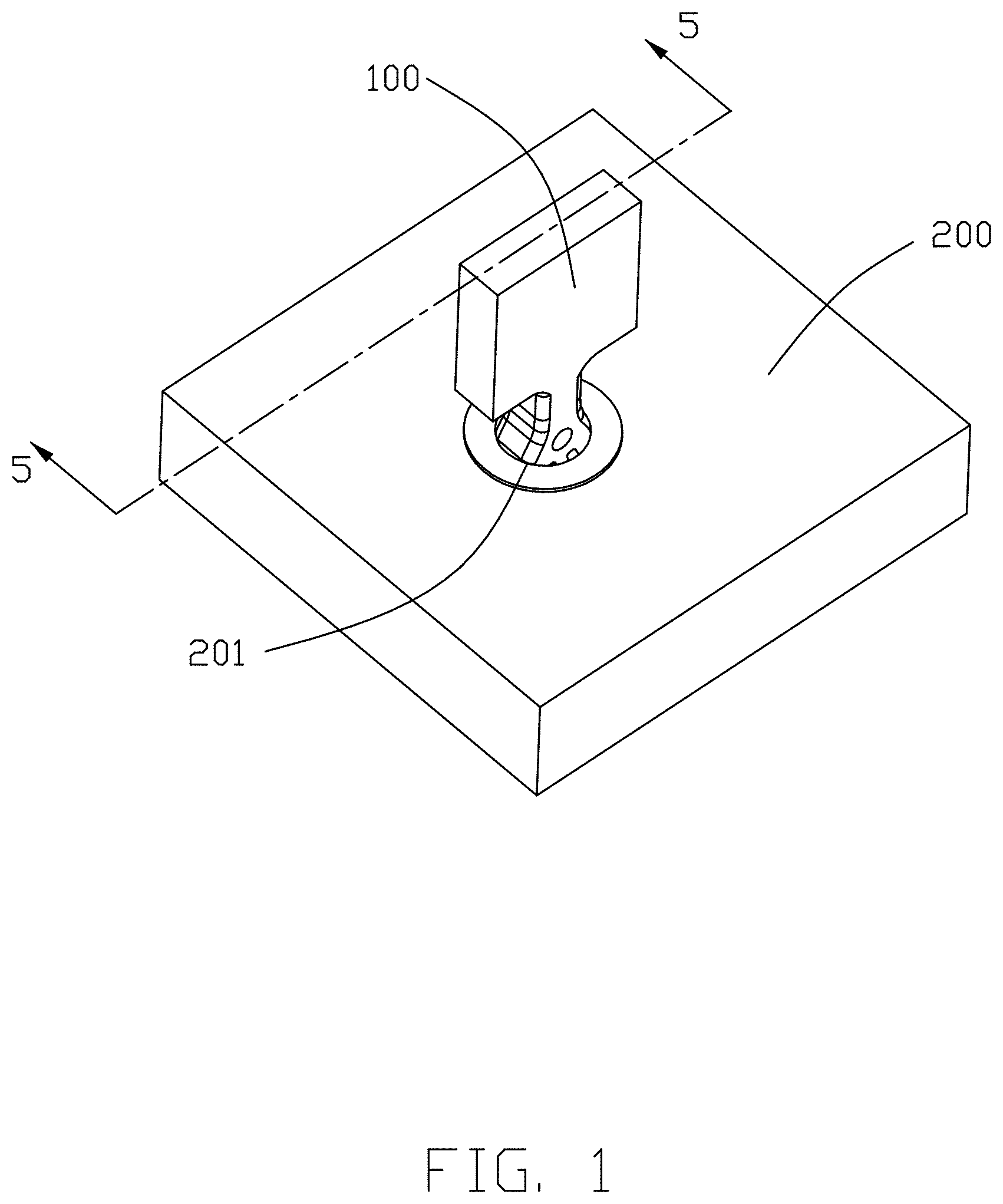
FIG. 1 is a top perspective view of an electrical contact assembled to a printed circuit board according to a first embodiment of the invention;
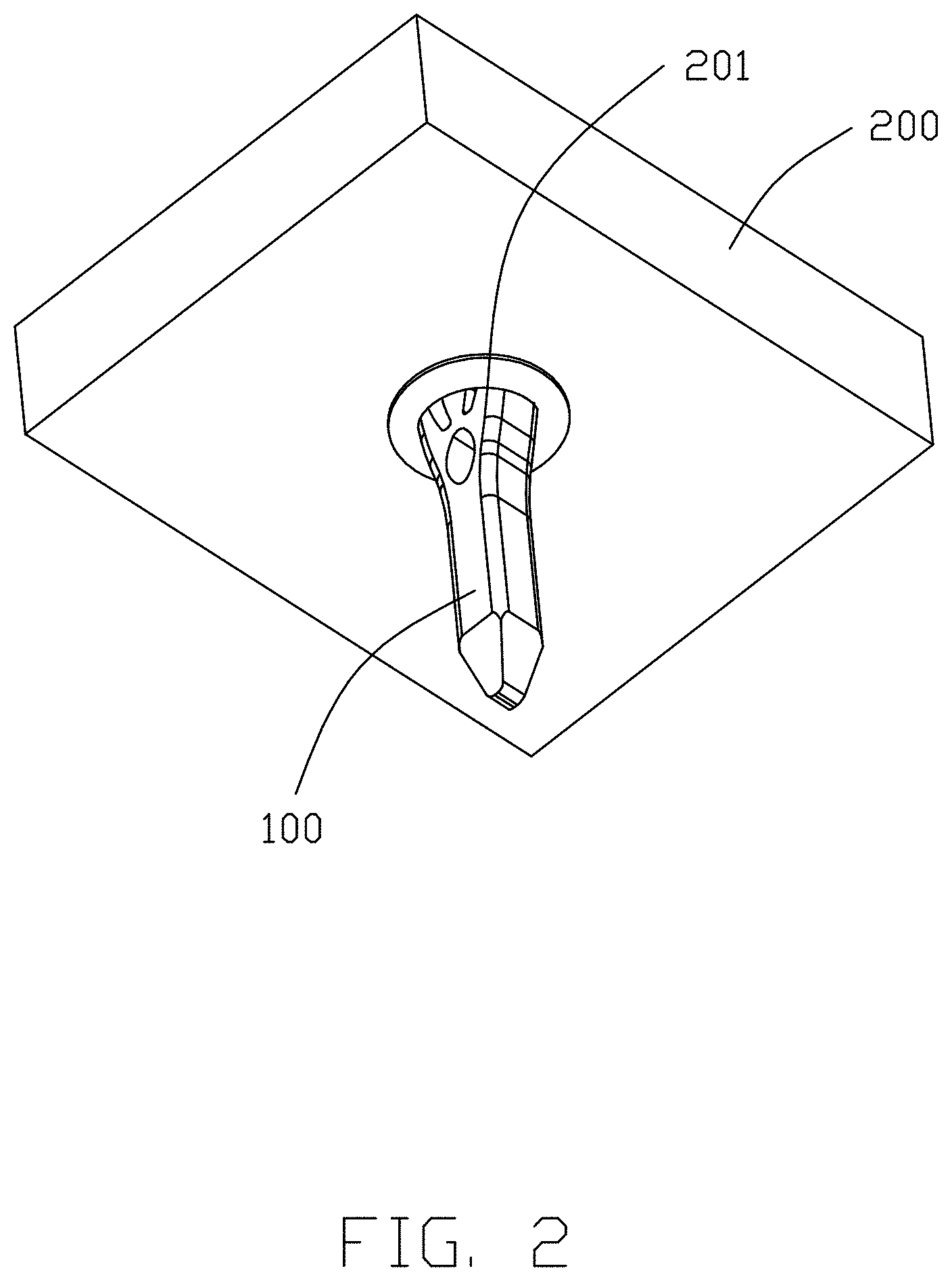
FIG. 2 is a bottom perspective view of the assembled electrical contact and printed circuit board of FIG. 1;
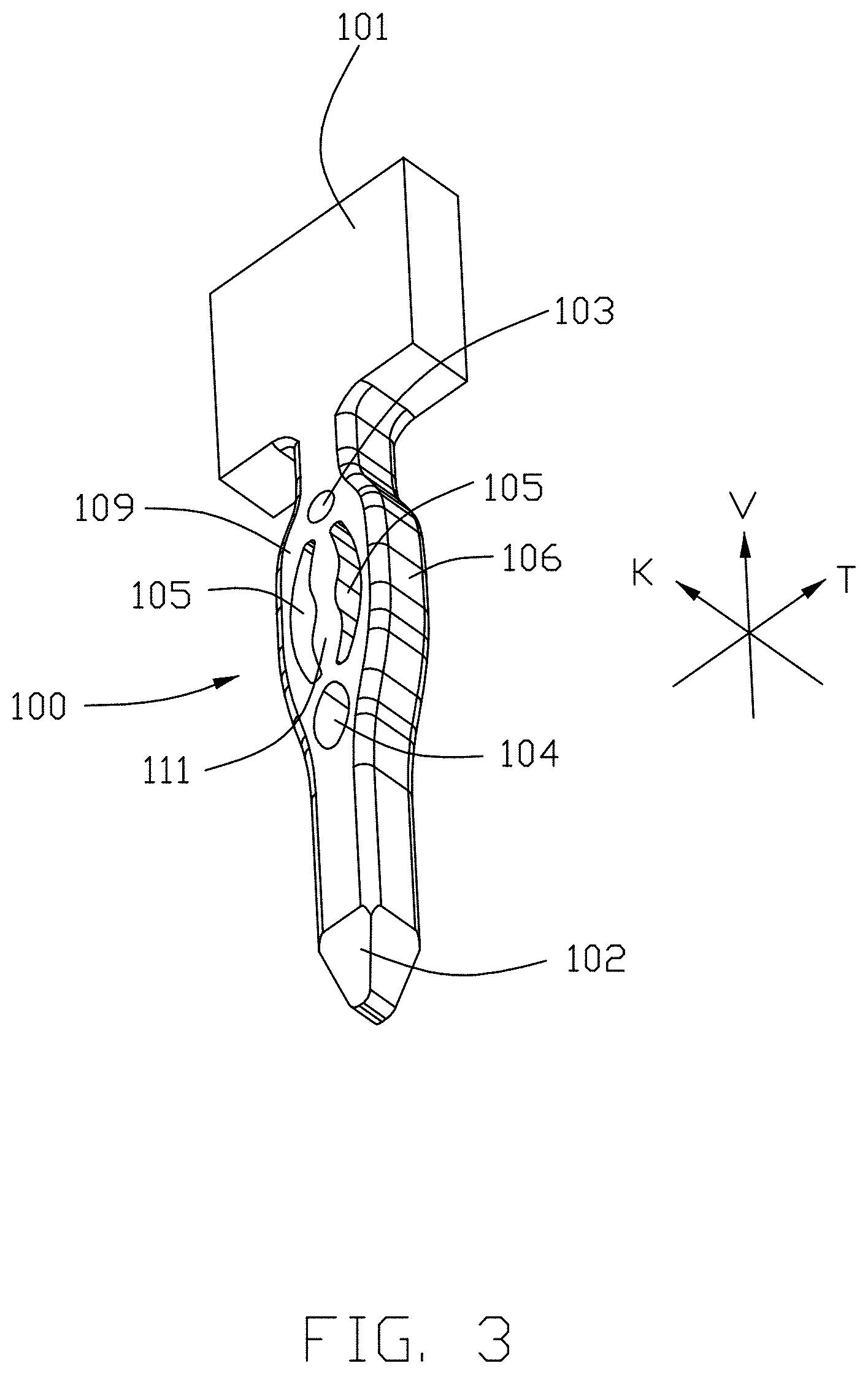
FIG. 3 is a perspective view of the electrical contact of FIG. 1;
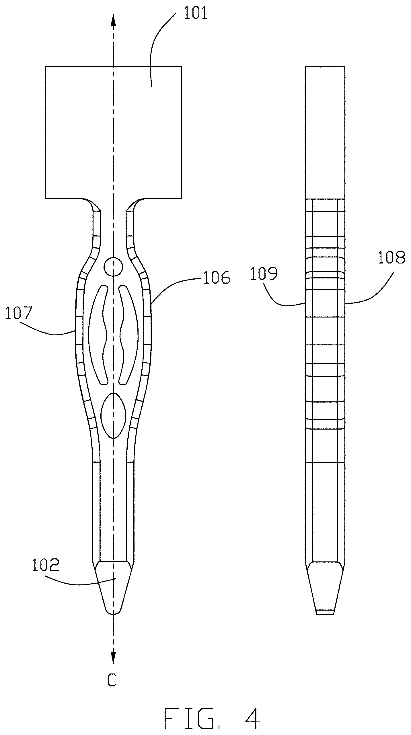
FIG. 4 is elevantional views of the electrical contact of FIG. 3;
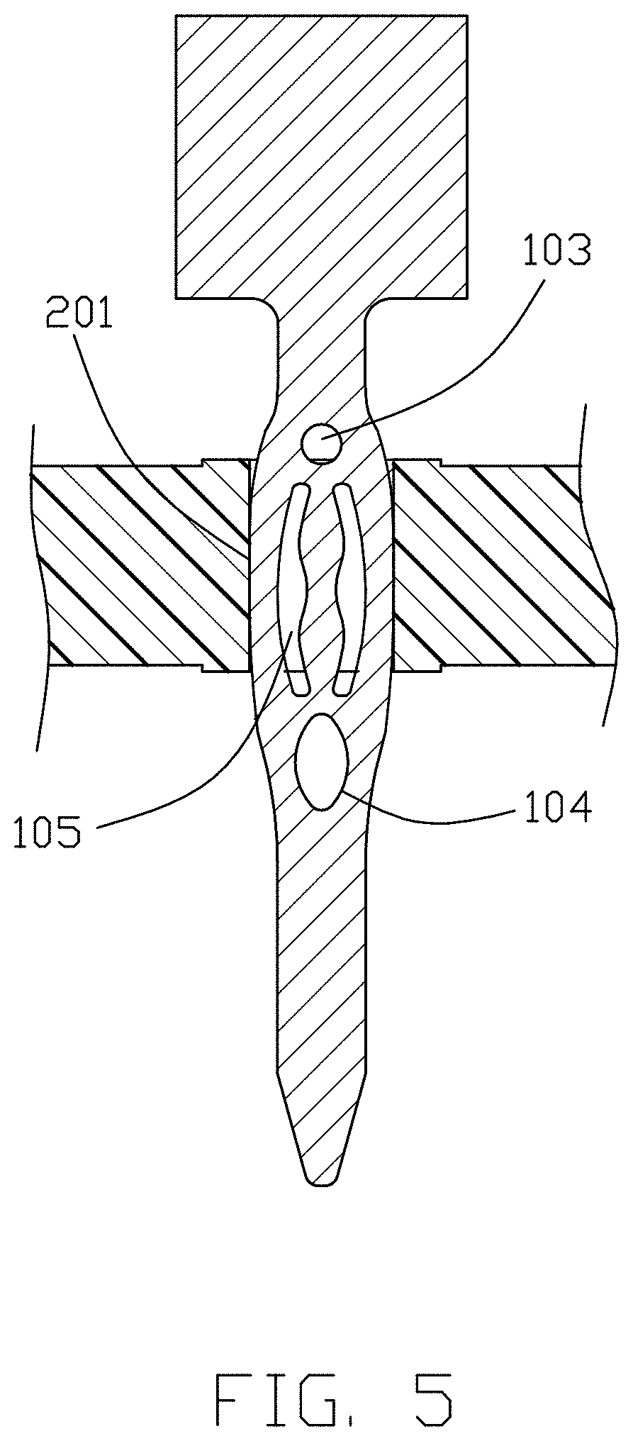
FIG. 5 is across-sectional view of the assembled electrical contact in the printed circuit board of FIG. 1;
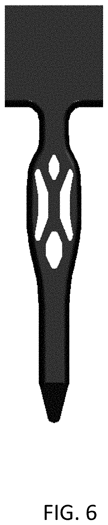
FIG. 6 is an elevational view of the electrical contact according to a second embodiment of the invention; and
FIG. 6(A) is an enlarged elevantional view of the retention section of the contact tail of the electrical contact of FIG. 6.
DETAILED DESCRIPTION OF THE PREFERRED EMBODIMENT
Referring to FIGS. 1-5, an electrical contact stamped from shell metal, includes a compliant tail 100 for mounting into a through/positioning hole 201 of a printed circuit board 200. The contact includes a head 101 extending upwardly from the compliant tail 100, and a free end 102 located at the bottom of the compliant tail 100. The compliant tail 100 includes a pair of opposite first main face 108 and second main face 109, and a pair of opposite first side face 106 and second side face 107 linked between the pair of first main face 108 and second main face 109 wherein the first side face 106 and the second side face 107 are bulged for elastically pressing an interior surface of the positioning hole 201. In other words, the maximum width of the compliant leg 100 around the bulged area. i.e., the retention section, is slightly larger than a diameter of the positioning hole 201.
A pair of first holes 105 and a pair of second holes 103/104 extend through the complaint leg 100 in the thickness direction K. The pair of first holes 105 are located on two sides of the bulged area in the transverse direction T perpendicular to the thickness direction K, and extending in the vertical/top-to-bottom direction V perpendicular to both the thickness direction K and the transverse direction T. In other words, the pair of first holes 105 are symmetrical with each other with regard to the centerline C of the compliant tail 100 which extends in the vertical direction V. Notably, the pair of first holes 105 are configured to be inwardly bowed like of a partial moon toward each other. Specifically, in the compliant tail 100 the rib or divider 111 formed between the pair of first holes 105 in the transverse direction T and extending along the centerline C, forms a calabash configuration so as to counterbalance the contour of the bulged area when the bulged area is inwardly pressed in the positioning hole 201.
The pair of second holes 103/104 are respectively located around the top ends and the bottom ends of the pair of first holes 105 in the vertical direction V. The elliptical second hole 104 is larger than the round second hole 103. As shown in FIG. 5, during mounting to the printed circuit board 200, the pair of second holes 103/104 are exposed outside of the positioning hole 201 and respectively above the top surface and below the bottom surface of the printed circuit board 200. In this embodiment, the pair of second holes 103/104 are located at the centerline C and respectively aligned with and located above a top end and below a bottom end of the rib 111. In this embodiment, in the retention section, a width, i.e., the dimension along the transverse direction, of the upper region where the second hole 103 is located, is slightly larger than that of the lower region where the second hole 104 is located. In other words, the slope of the lower region is smaller than that of the upper region for facilitating insertion of the compliant tail 100 into the positioning hole 201.
Referring to FIGS. 6 and 6(A) showing the second embodiment, the pair of first (left and right) holes L/R and the pair of second (top/bottom) holes UB are arranged with an X-configuration rib formed thereamong wherein viewed along the transverse direction T, the bottom hole B and the right hole R are overlapped between line L1 and line L2; viewed along the vertical direction V, the bottom hole B and the right hole R are overlapped between line L3 and line L4. Notably, the similar relation is applied to other neighboring holes. Notably, in the first embodiment, the first holes and the second holes are not overlapped when viewed in the transverse direction. In the second embodiment, both second holes U and B are configured with a fish eye configuration, and both holes L and R are configured to be outwardly bowed away from each other.
However, the disclosure is illustrative only, changes may be made in detail, especially in matter of shape, size, and arrangement of sections within the principles of the invention.
* * * * *
D00000
D00001
D00002
D00003
D00004
D00005
D00006
D00007
XML
uspto.report is an independent third-party trademark research tool that is not affiliated, endorsed, or sponsored by the United States Patent and Trademark Office (USPTO) or any other governmental organization. The information provided by uspto.report is based on publicly available data at the time of writing and is intended for informational purposes only.
While we strive to provide accurate and up-to-date information, we do not guarantee the accuracy, completeness, reliability, or suitability of the information displayed on this site. The use of this site is at your own risk. Any reliance you place on such information is therefore strictly at your own risk.
All official trademark data, including owner information, should be verified by visiting the official USPTO website at www.uspto.gov. This site is not intended to replace professional legal advice and should not be used as a substitute for consulting with a legal professional who is knowledgeable about trademark law.