Semiconductor device with substrate temperature monitor circuit
Komo , et al. Dec
U.S. patent number 10,505,518 [Application Number 15/520,636] was granted by the patent office on 2019-12-10 for semiconductor device with substrate temperature monitor circuit. This patent grant is currently assigned to Mitsubishi Electric Corporation. The grantee listed for this patent is Mitsubishi Electric Corporation. Invention is credited to Hideo Komo, Takeshi Omaru, Koichi Taguchi.


| United States Patent | 10,505,518 |
| Komo , et al. | December 10, 2019 |
Semiconductor device with substrate temperature monitor circuit
Abstract
First and second circuits, a photocoupler and a substrate temperature monitor circuit are formed on a substrate. A photocoupler includes a primary-side light emitting diode that converts an electric signal received from the first circuit into an optical signal, and a light receiving device that converts the optical signal into an electric signal and outputs the electric signal to the second circuit. The substrate temperature monitor circuit reads a Vf voltage value of the primary-side light emitting diode of the photocoupler to monitor temperature of the substrate.
| Inventors: | Komo; Hideo (Tokyo, JP), Taguchi; Koichi (Fukuoka, JP), Omaru; Takeshi (Tokyo, JP) | ||||||||||
|---|---|---|---|---|---|---|---|---|---|---|---|
| Applicant: |
|
||||||||||
| Assignee: | Mitsubishi Electric Corporation
(Tokyo, JP) |
||||||||||
| Family ID: | 56416596 | ||||||||||
| Appl. No.: | 15/520,636 | ||||||||||
| Filed: | January 20, 2015 | ||||||||||
| PCT Filed: | January 20, 2015 | ||||||||||
| PCT No.: | PCT/JP2015/051393 | ||||||||||
| 371(c)(1),(2),(4) Date: | April 20, 2017 | ||||||||||
| PCT Pub. No.: | WO2016/117030 | ||||||||||
| PCT Pub. Date: | July 28, 2016 |
Prior Publication Data
| Document Identifier | Publication Date | |
|---|---|---|
| US 20170317664 A1 | Nov 2, 2017 | |
| Current U.S. Class: | 1/1 |
| Current CPC Class: | G01K 7/00 (20130101); G01K 3/10 (20130101); H01L 25/167 (20130101); H03K 3/017 (20130101); G01K 7/01 (20130101); H01G 9/0003 (20130101); H03K 3/011 (20130101); H01G 9/28 (20130101); H01L 31/167 (20130101); H01L 31/12 (20130101) |
| Current International Class: | H03K 3/011 (20060101); G01K 7/01 (20060101); H01L 31/12 (20060101); H03K 3/017 (20060101); H01L 31/167 (20060101); H01L 25/16 (20060101); G01K 3/10 (20060101); G01K 7/00 (20060101); H01G 9/00 (20060101); H01G 9/28 (20060101) |
References Cited [Referenced By]
U.S. Patent Documents
| 6255891 | July 2001 | Matsuno |
| 6851849 | February 2005 | Kimura |
| 2003/0038332 | February 2003 | Kimura |
| 2005/0285228 | December 2005 | Sugawara |
| 2006/0284124 | December 2006 | Aki |
| 2013/0060499 | March 2013 | Yoshimura |
| 2016/0258821 | September 2016 | Tsurumaru |
| 1701439 | Nov 2005 | CN | |||
| 1881552 | Dec 2006 | CN | |||
| 102564627 | Jul 2012 | CN | |||
| 102998017 | Mar 2013 | CN | |||
| Sho62-218155 | Sep 1987 | JP | |||
| 2004-310473 | Nov 2004 | JP | |||
| 2005-268262 | Sep 2005 | JP | |||
| 2005268262 | Sep 2005 | JP | |||
| 2006-351859 | Dec 2006 | JP | |||
| 2007-201169 | Aug 2007 | JP | |||
| 2008-306193 | Dec 2008 | JP | |||
| 2012-023826 | Feb 2012 | JP | |||
| 2012023826 | Feb 2012 | JP | |||
| 2013-053783 | Mar 2013 | JP | |||
| 2013-130346 | Jul 2013 | JP | |||
| 2013/065731 | May 2013 | WO | |||
| 2013168104 | Nov 2013 | WO | |||
Other References
|
An Office Action mailed by the State Intellectual Property Office of the People's Republic of China dated Jul. 3, 2018, which corresponds to Chinese Patent Application No. 201580074020.6 and is related to U.S. Appl. No. 15/520,636. cited by applicant . An Office Action; "Notification of Reasons for Refusal," mailed by the Japanese Patent Office dated Jan. 23, 2018, which corresponds to Japanese Patent Application No. 2016-570377 and is related to U.S. Appl. No. 15/520,636; with English language translation. cited by applicant . International Search Report issued in PCT/JP2015/051393; dated Mar. 10, 2015. cited by applicant . An Office Action mailed by the State Intellectual Property Office of People's Republic of China dated Mar. 27, 2019, which corresponds to Chinese Patent Application No. 201580074020.6 and is related to U.S. Appl. No. 15/520,636. cited by applicant . An Office Action mailed by the State Intellectual Property Office of People's Republic of China dated Oct. 22, 2019, which corresponds to Chinese Patent Application No. 201580074020.6 and is related to U.S. Appl. No. 15/520,636. cited by applicant. |
Primary Examiner: Fureman; Jared
Assistant Examiner: Warmflash; Michael J
Attorney, Agent or Firm: Studebaker & Brackett PC
Claims
The invention claimed is:
1. A semiconductor device comprising: a substrate; first and second circuits formed on the substrate; a photocoupler formed on the substrate and including a light emitting diode that converts an electric signal received from the first circuit into an optical signal, and a light receiving device that converts the optical signal into an electric signal and outputs the electric signal to the second circuit; a substrate temperature monitor circuit reading a Vf voltage value of the light emitting diode of the photocoupler to monitor temperature of the substrate; and a power supply circuit supplying a voltage to each of the first and second circuits, wherein the substrate temperature monitor circuit corrects a temperature variation in an output voltage value of the power supply circuit according to the monitored temperature of the substrate.
2. The semiconductor device according to claim 1, wherein the power supply circuit is a single power supply circuit that supplies the voltage to each of the first and second circuits in parallel.
3. A semiconductor device comprising: a substrate; first and second circuits formed on the substrate; a photocoupler formed on the substrate and including a light emitting diode that converts an electric signal received from the first circuit into an optical signal, and a light receiving device that converts the optical signal into an electric signal and outputs the electric signal to the second circuit; a substrate temperature monitor circuit reading a Vf voltage value of the light emitting diode of the photocoupler to monitor temperature of the substrate; and a power supply circuit supplying a voltage to each of the first and second circuits, wherein the power supply circuit includes an aluminum electrolytic capacitor, and the substrate temperature monitor circuit accumulates thermal histories of the aluminum electrolytic capacitor from the monitored temperature of the substrate to predict a life of the aluminum electrolytic capacitor.
4. The semiconductor device according to claim 3, wherein the substrate temperature monitor circuit outputs an error signal when the predicted life of the aluminum electrolytic capacitor has reached life criteria.
5. The semiconductor device according to claim 3, wherein the power supply circuit is a single power supply circuit that supplies the voltage to each of the first and second circuits in parallel.
6. A semiconductor device comprising: a substrate; first and second circuits formed on the substrate; a photocoupler formed on the substrate and including a light emitting diode that converts an electric signal received from the first circuit into an optical signal, and a light receiving device that converts the optical signal into an electric signal and outputs the electric signal to the second circuit; and a substrate temperature monitor circuit reading a Vf voltage value of the light emitting diode of the photocoupler to monitor temperature of the substrate, wherein the photocoupler includes a plurality of photocouplers, and the substrate temperature monitor circuit reads the Vf voltage value of the light emitting diode of each of the plurality of photocouplers and averages the read voltage values to monitor the temperature of the substrate.
7. The semiconductor device according to claim 6, wherein the plurality of photocouplers are each formed on the same substrate.
Description
FIELD
The present invention relates to a semiconductor device capable of monitoring a substrate temperature without the need for adding any components.
BACKGROUND
A control system for a semiconductor device is required to achieve a high precision, a high functionality, and a high packaging density at a low cost. In the control system, an improvement in the precision of various sensing functions is one of important problems to be solved to achieve an improvement in the efficiency of the semiconductor device. One of impediments to the achievement of an improvement in precision is a variation in performance due to temperature characteristics of electronic components. Accordingly, it is necessary to take some measures to reduce the variation in performance.
Note that a photocoupler is an electronic component that is generally used to transmit signals from a logic part and a semiconductor device, while providing electrical isolation between the logic part and the semiconductor device. A technique in which a light emitting diode of a photocoupler detects abnormal heat generation in the photocoupler has been proposed (e.g., see PTL 1).
CITATION LIST
Patent Literature
[PTL 1] JP 2007-201169 A
SUMMARY
Technical Problem
To reduce a variation in performance of sensing functions due to temperature characteristics of electronic components, it is necessary to monitor the temperature of a substrate and feed back the monitored temperature. Accordingly, monitoring the substrate temperature using a thermocouple or a thermistor causes a problem that the number of components and costs increase.
The present invention has been made to solve the above-mentioned problem, and an object of the present invention is to obtain a semiconductor device capable of monitoring a substrate temperature without the need for adding any components.
Solution to Problem
A semiconductor device according to the present invention includes: a substrate; first and second circuits formed on the substrate; a photocoupler formed on the substrate and including a light emitting diode that converts an electric signal received from the first circuit into an optical signal, and a light receiving device that converts the optical signal into an electric signal and outputs the electric signal to the second circuit; and a substrate temperature monitor circuit reading a Vf voltage value of the light emitting diode of the photocoupler to monitor temperature of the substrate.
Advantageous Effects of Invention
In the present invention, the substrate temperature monitor circuit reads the Vf voltage value of the light emitting diode of the photocoupler to monitor the temperature of the substrate. Therefore, the photocoupler can monitor the temperature of the substrate, without the need for adding a component such as a thermocouple or a thermistor.
BRIEF DESCRIPTION OF THE DRAWINGS
FIG. 1 is a diagram showing a semiconductor device according to Embodiment 1 of the present invention.
FIG. 2 is a graph showing Vf voltage characteristics of the light emitting diode of the photocoupler.
FIG. 3 is a diagram showing a semiconductor device according to Embodiment 2 of the present invention.
FIG. 4 is a diagram showing a semiconductor device according to Embodiment 3 of the present invention.
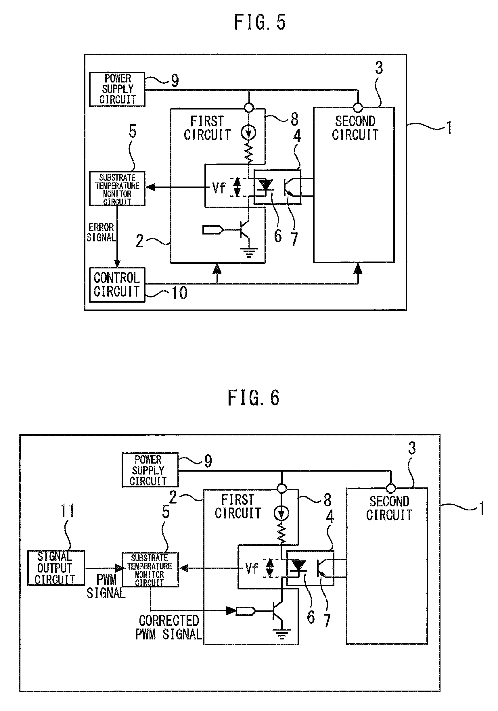
FIG. 5 is a diagram showing a semiconductor device according to Embodiment 4 of the present invention.
FIG. 6 is a diagram showing a semiconductor device according to Embodiment 5 of the present invention.
FIG. 7 is a diagram showing a semiconductor device according to Embodiment 6 of the present invention.
FIG. 8 is a graph showing a life curve of the aluminum electrolytic capacitor.
FIG. 9 is a diagram showing a semiconductor device according to Embodiment 7 of the present invention.
FIG. 10 is a diagram showing a semiconductor device according to Embodiment 8 of the present invention.
DESCRIPTION OF EMBODIMENTS
A semiconductor device according to the embodiments of the present invention will be described with reference to the drawings. The same components will be denoted by the same symbols, and the repeated description thereof may be omitted.
Embodiment 1
FIG. 1 is a diagram showing a semiconductor device according to Embodiment 1 of the present invention. On a substrate 1, first and second circuits 2 and 3, a photocoupler 4, and a substrate temperature monitor circuit 5 are formed. The photocoupler 4 includes a primary-side light emitting diode 6 that converts an electric signal received from the first circuit 2 into an optical signal, and a light receiving device 7 that converts the optical signal into an electric signal and outputs the electric signal to the second circuit 3. The photocoupler 4 transmits signals from the first circuit 2 and the second circuit 3, while providing electrical isolation between the first circuit 2 and the second circuit 3.
FIG. 2 is a graph showing Vf voltage characteristics of the light emitting diode of the photocoupler. As shown in the figure, the Vf voltage of the primary-side light emitting diode 6 has a temperature dependence. Accordingly, the substrate temperature monitor circuit 5 reads the Vf voltage value of the primary-side light emitting diode 6 of the photocoupler 4, thereby monitoring the temperature of the substrate 1. Since the photocoupler 4 is originally equipped in the device, the photocoupler 4 can monitor the temperature of the substrate 1, without the need for adding a component such as a thermocouple or a thermistor. The monitored temperature is fed back to various sensing circuits to cancel a variation in circuit characteristics due to the temperature, thereby achieving an improvement in the precision of sensing functions.
Embodiment 2
FIG. 3 is a diagram showing a semiconductor device according to Embodiment 2 of the present invention. A constant current circuit 8 is used as a drive circuit for the primary-side light emitting diode 6. With this configuration, substrate temperature information can be accurately monitored.
Embodiment 3
FIG. 4 is a diagram showing a semiconductor device according to Embodiment 3 of the present invention. A power supply circuit 9 supplies a voltage to each of the first and second circuits 2 and 3. The substrate temperature monitor circuit 5 corrects a temperature variation in the output voltage value of the power supply circuit 9 according to the monitored temperature of the substrate 1. Thus, the temperature information is fed back to the power supply circuit 9 and a variation in the power supply voltage value due to temperature characteristics is corrected, thereby making it possible to improve the precision of the drive system for the semiconductor device.
Embodiment 4
FIG. 5 is a diagram showing a semiconductor device according to Embodiment 4 of the present invention. The substrate temperature monitor circuit 5 outputs an error signal when the monitored temperature of the substrate 1 has reached a threshold. A control circuit 10 which has received the error signal interrupts the operation of each of the first and second circuits 2 and 3. Thus, the error signal is output during abnormal heat generation in the substrate 1, thereby making it possible to properly protect the semiconductor device.
Embodiment 5
FIG. 6 is a diagram showing a semiconductor device according to Embodiment 5 of the present invention. A signal output circuit 11 outputs a pulse width modulation (PWM) signal. The substrate temperature monitor circuit 5 corrects a PWM signal according to the monitored temperature of the substrate 1 and supplies the PWM signal to the photocoupler 4. Thus, the temperature is monitored by the substrate temperature monitor circuit 5 and the monitored temperature is fed back, thereby making it possible to correct a variation in transmission of a duty of the PWM signal of the photocoupler 4 that is caused due to temperature characteristics.
Embodiment 6
FIG. 7 is a diagram showing a semiconductor device according to Embodiment 6 of the present invention. The power supply circuit 9 includes an aluminum electrolytic capacitor 12. The substrate temperature monitor circuit 5 refers to a preliminarily stored life curve of the aluminum electrolytic capacitor 12, and accumulates thermal histories of the aluminum electrolytic capacitor 12 from the monitored temperature of the substrate 1, to thereby predict the life of the aluminum electrolytic capacitor 12. FIG. 8 is a graph showing a life curve of the aluminum electrolytic capacitor. Based on this life curve, the life of the aluminum electrolytic capacitor 12 can be accurately predicted.
The substrate temperature monitor circuit 5 outputs an error signal when the predicted life of the aluminum electrolytic capacitor 12 has reached life criteria. An error output part 13 which has received the error signal notifies a user of the error by display, voice, or the like. Thus, the semiconductor device can be properly protected, and a time for replacement of the semiconductor device can be detected.
Embodiment 7
FIG. 9 is a diagram showing a semiconductor device according to Embodiment 7 of the present invention. A plurality of photocouplers 4 is formed on the substrate 1. Although the illustration of the first and second circuits 2 and 3 and the like is omitted, the configurations of these components are similar to those of any one of Embodiments 1 to 6.
The substrate temperature monitor circuit 5 reads the Vf voltage value of the primary-side light emitting diode 6 of each of the plurality of photocouplers 4, and averages the read voltage values, thereby monitoring the temperature of the substrate 1. Thus, the temperature of the substrate is monitored by the plurality of photocouplers 4, thereby making it possible to more accurately monitor the temperature of the substrate 1.
Embodiment 8
FIG. 10 is a diagram showing a semiconductor device according to Embodiment 8 of the present invention. A plurality of photocouplers 4 is formed on the substrate 1. Although the illustration of the first and second circuits 2 and 3 and the like is omitted, the configurations of these components are similar to those of any one of Embodiments 1 to 6.
The substrate temperature monitor circuit 5 reads the Vf voltage value of the primary-side light emitting diode 6 of the photocoupler 4 that is located at a position where the temperature of the substrate 1 is highest among the plurality of photocouplers 4, thereby monitoring the temperature of the substrate 1. Thus, one of the photocouplers 4 is monitored, thereby minimizing the cost and sensing processing.
REFERENCE SIGNS LIST
1 substrate; 2 first circuit; 3 second circuit; 4 photocoupler; 5 substrate temperature monitor circuit; 6 primary-side light emitting diode; 7 light receiving device; 8 constant current circuit; 9 power supply circuit; 10 control circuit; 11 signal output circuit; 12 aluminum electrolytic capacitor
* * * * *
D00000
D00001
D00002
D00003
D00004
D00005
XML
uspto.report is an independent third-party trademark research tool that is not affiliated, endorsed, or sponsored by the United States Patent and Trademark Office (USPTO) or any other governmental organization. The information provided by uspto.report is based on publicly available data at the time of writing and is intended for informational purposes only.
While we strive to provide accurate and up-to-date information, we do not guarantee the accuracy, completeness, reliability, or suitability of the information displayed on this site. The use of this site is at your own risk. Any reliance you place on such information is therefore strictly at your own risk.
All official trademark data, including owner information, should be verified by visiting the official USPTO website at www.uspto.gov. This site is not intended to replace professional legal advice and should not be used as a substitute for consulting with a legal professional who is knowledgeable about trademark law.