Waveguide optics focus elements
Robbins , et al. Dec
U.S. patent number 10,502,876 [Application Number 13/477,646] was granted by the patent office on 2019-12-10 for waveguide optics focus elements. This patent grant is currently assigned to Microsoft Technology Licensing, LLC. The grantee listed for this patent is David D. Bohn, Ian Anh Nguyen, Steven John Robbins. Invention is credited to David D. Bohn, Ian Anh Nguyen, Steven John Robbins.
| United States Patent | 10,502,876 |
| Robbins , et al. | December 10, 2019 |
Waveguide optics focus elements
Abstract
In embodiments of waveguide optics focus elements, an imaging structure includes a waveguide for viewing of an environment that is viewable with the imaging structure. The waveguide transmits light of a virtual image that is generated to appear as part of the environment for augmented-reality imaging or virtual-reality imaging. The imaging structure also includes one or more focus elements that are integrated in the waveguide and switchable to focus the virtual image at a focus depth that approximately correlates to a focal distance of the environment. The focus elements can each be implemented for a different focus depth of the virtual image, and the focus depth is adjustable based on a combination of the focus elements being switched-on or switched-off.
| Inventors: | Robbins; Steven John (Bellevue, WA), Nguyen; Ian Anh (Bellevue, WA), Bohn; David D. (Fort Collins, CO) | ||||||||||
|---|---|---|---|---|---|---|---|---|---|---|---|
| Applicant: |
|
||||||||||
| Assignee: | Microsoft Technology Licensing,
LLC (Redmond, WA) |
||||||||||
| Family ID: | 49621407 | ||||||||||
| Appl. No.: | 13/477,646 | ||||||||||
| Filed: | May 22, 2012 |
Prior Publication Data
| Document Identifier | Publication Date | |
|---|---|---|
| US 20130314793 A1 | Nov 28, 2013 | |
| Current U.S. Class: | 1/1 |
| Current CPC Class: | G02B 27/0172 (20130101); G02B 5/18 (20130101); G02B 2027/0127 (20130101); G02B 2027/0134 (20130101) |
| Current International Class: | G02B 5/18 (20060101); G02B 27/01 (20060101) |
| Field of Search: | ;359/629-634 ;345/6-9,632-633 |
References Cited [Referenced By]
U.S. Patent Documents
| 3410774 | November 1968 | Barson et al. |
| 3836258 | September 1974 | Courten et al. |
| 3906528 | September 1975 | Johnson |
| 3971065 | July 1976 | Bayer |
| 4711512 | December 1987 | Upatnieks |
| 4822145 | April 1989 | Staelin |
| 4860361 | August 1989 | Sato et al. |
| 4957351 | September 1990 | Shioji |
| 5019808 | May 1991 | Prince et al. |
| 5146355 | September 1992 | Prince et al. |
| 5252950 | October 1993 | Saunders et al. |
| 5309169 | May 1994 | Leppert |
| 5359444 | October 1994 | Piosenka et al. |
| 5453877 | September 1995 | Gerbe et al. |
| 5455458 | October 1995 | Quon et al. |
| 5455601 | October 1995 | Ozaki |
| 5455882 | October 1995 | Veligdan |
| 5459611 | October 1995 | Bohn et al. |
| 5483307 | January 1996 | Anderson |
| 5491580 | February 1996 | O'Meara |
| 5543588 | August 1996 | Bisset et al. |
| 5574473 | November 1996 | Sekiguchi |
| 5579830 | December 1996 | Giammaruti |
| 5583609 | December 1996 | Mizutani et al. |
| 5606455 | February 1997 | Eichenlaub |
| 5614941 | March 1997 | Hines |
| 5648643 | July 1997 | Knowles et al. |
| 5651414 | July 1997 | Suzuki et al. |
| 5673146 | September 1997 | Kelly |
| 5708449 | January 1998 | Heacock et al. |
| 5714967 | February 1998 | Okamura et al. |
| 5737171 | April 1998 | Buller et al. |
| 5751476 | May 1998 | Matsui et al. |
| 5771320 | June 1998 | Stone |
| 5777715 | July 1998 | Kruegle et al. |
| 5856842 | January 1999 | Tedesco |
| 5861931 | January 1999 | Gillian et al. |
| 5886822 | March 1999 | Spitzer |
| 5940149 | August 1999 | Vanderwerf |
| 5959664 | September 1999 | Woodgate |
| 5982553 | November 1999 | Bloom et al. |
| 5991087 | November 1999 | Rallison |
| 6101008 | August 2000 | Popovich |
| 6144439 | November 2000 | Carollo |
| 6160667 | December 2000 | Smoot |
| 6188427 | February 2001 | Anderson et al. |
| 6226178 | May 2001 | Broder et al. |
| 6239502 | May 2001 | Grewe et al. |
| 6264787 | July 2001 | Burbank |
| 6271808 | August 2001 | Corbin |
| 6307142 | October 2001 | Allen et al. |
| 6323970 | November 2001 | Popovich |
| 6377401 | April 2002 | Bartlett |
| 6411512 | June 2002 | Mankaruse et al. |
| 6446442 | September 2002 | Batchelor et al. |
| 6466198 | October 2002 | Feinstein |
| 6470289 | October 2002 | Peters et al. |
| 6481851 | November 2002 | McNelley et al. |
| 6496218 | December 2002 | Takigawa et al. |
| 6525847 | February 2003 | Popovich |
| 6529331 | March 2003 | Massof et al. |
| 6542307 | April 2003 | Gleckman et al. |
| 6545650 | April 2003 | Yamada et al. |
| 6547416 | April 2003 | Pashley et al. |
| 6554428 | April 2003 | Fergason et al. |
| 6567101 | May 2003 | Thomas |
| 6577411 | June 2003 | David |
| 6580529 | June 2003 | Amitai et al. |
| 6606152 | August 2003 | Littau |
| 6621702 | September 2003 | Elias et al. |
| 6631755 | October 2003 | Kung et al. |
| 6635999 | October 2003 | Belliveau |
| 6639201 | October 2003 | Almogy et al. |
| 6735499 | May 2004 | Ohki et al. |
| 6753828 | June 2004 | Tuceryan et al. |
| 6775460 | August 2004 | Steiner et al. |
| 6804115 | October 2004 | Lai |
| 6809925 | October 2004 | Belady et al. |
| 6825987 | November 2004 | Repetto et al. |
| 6829095 | December 2004 | Amitai |
| 6867753 | March 2005 | Chinthammit et al. |
| 6888613 | May 2005 | Robins et al. |
| 6889755 | May 2005 | Zuo et al. |
| 6906901 | June 2005 | Liu |
| 6919867 | July 2005 | Sauer |
| 6947020 | September 2005 | Kiser et al. |
| 6964731 | November 2005 | Krisko et al. |
| 6971443 | December 2005 | Kung et al. |
| 6992738 | January 2006 | Ishihara et al. |
| 6997241 | February 2006 | Chou et al. |
| 7006215 | February 2006 | Hoff et al. |
| 7015876 | March 2006 | Miller |
| 7048385 | May 2006 | Beeson et al. |
| 7069975 | July 2006 | Haws et al. |
| 7113605 | September 2006 | Rui et al. |
| 7116555 | October 2006 | Kamath et al. |
| 7184615 | February 2007 | Levola |
| 7191820 | March 2007 | Chou et al. |
| 7193584 | March 2007 | Lee et al. |
| 7250930 | July 2007 | Hoffman et al. |
| 7261453 | August 2007 | Morejon et al. |
| 7271795 | September 2007 | Bradski |
| 7277282 | October 2007 | Tate |
| 7301587 | November 2007 | Uehara et al. |
| 7337018 | February 2008 | Espinoza-Ibarra et al. |
| 7359420 | April 2008 | Shchegrov et al. |
| 7365734 | April 2008 | Fateh et al. |
| 7369101 | May 2008 | Sauer et al. |
| 7376852 | May 2008 | Edwards |
| 7396133 | July 2008 | Burnett et al. |
| 7412306 | August 2008 | Katoh et al. |
| 7416017 | August 2008 | Haws et al. |
| 7417617 | August 2008 | Eichenlaub |
| 7418170 | August 2008 | Mukawa et al. |
| 7428001 | September 2008 | Schowengerdt et al. |
| 7430349 | September 2008 | Jones |
| 7430355 | September 2008 | Heikenfeld et al. |
| 7455102 | November 2008 | Cheng |
| 7505269 | March 2009 | Cosley et al. |
| 7513627 | April 2009 | Larson et al. |
| 7515143 | April 2009 | Keam et al. |
| 7542665 | June 2009 | Lei |
| 7551814 | June 2009 | Smits |
| 7576916 | August 2009 | Amitai |
| 7583327 | September 2009 | Takatani |
| 7607111 | October 2009 | Vaananen et al. |
| 7619895 | November 2009 | Wertz et al. |
| 7631687 | December 2009 | Yang |
| 7646606 | January 2010 | Rytka et al. |
| 7649594 | January 2010 | Kim et al. |
| 7660500 | February 2010 | Konttinen et al. |
| 7679641 | March 2010 | Lipton et al. |
| 7693292 | April 2010 | Gross et al. |
| 7701716 | April 2010 | Blanco, Jr. et al. |
| 7719769 | May 2010 | Sugihara et al. |
| 7768534 | August 2010 | Pentenrieder et al. |
| 7777944 | August 2010 | Ho et al. |
| 7817104 | October 2010 | Ryu et al. |
| 7832885 | November 2010 | Hsiao et al. |
| 7843691 | November 2010 | Reichert et al. |
| 7868300 | January 2011 | Kruit et al. |
| 7894613 | February 2011 | Ong et al. |
| 7903409 | March 2011 | Patel et al. |
| 7909958 | March 2011 | Washburn et al. |
| 7941231 | May 2011 | Dunn |
| 7986462 | July 2011 | Kobayashi et al. |
| 8004621 | August 2011 | Woodgate et al. |
| 8033709 | October 2011 | Kao et al. |
| 8046616 | October 2011 | Edwards |
| 8061411 | November 2011 | Xu et al. |
| 8085948 | December 2011 | Thomas et al. |
| 8092064 | January 2012 | Erchak et al. |
| 8125579 | February 2012 | Khan et al. |
| 8160411 | April 2012 | Levola et al. |
| 8195220 | June 2012 | Kim et al. |
| 8233204 | July 2012 | Robbins et al. |
| 8233273 | July 2012 | Chen et al. |
| 8246170 | August 2012 | Yamamoto et al. |
| 8274614 | September 2012 | Yokote et al. |
| 8384999 | February 2013 | Crosby et al. |
| 8392035 | March 2013 | Patel et al. |
| 8395898 | March 2013 | Chamseddine et al. |
| 8418083 | April 2013 | Lundy et al. |
| 8446340 | May 2013 | Aharoni |
| 8472119 | June 2013 | Kelly |
| 8482920 | July 2013 | Tissot et al. |
| 8576143 | November 2013 | Kelly |
| 8611014 | December 2013 | Valera et al. |
| 8629815 | January 2014 | Brin et al. |
| 8638498 | January 2014 | Bohn et al. |
| 8645871 | February 2014 | Fong et al. |
| 8666212 | March 2014 | Amirparviz |
| 8712598 | April 2014 | Dighde et al. |
| 8754831 | June 2014 | Kollin et al. |
| 8770813 | July 2014 | Bohn et al. |
| 8810600 | August 2014 | Bohn et al. |
| 8817350 | August 2014 | Robbins et al. |
| 8823531 | September 2014 | McCleary et al. |
| 8854802 | October 2014 | Robinson et al. |
| 8909384 | December 2014 | Beitelmal et al. |
| 8917453 | December 2014 | Bohn |
| 8934235 | January 2015 | Rubenstein et al. |
| 8941683 | January 2015 | Son et al. |
| 8989535 | March 2015 | Robbins |
| 9052414 | June 2015 | Travis et al. |
| 9223138 | December 2015 | Bohn |
| 9272338 | March 2016 | Fujita et al. |
| 9297996 | March 2016 | Bohn et al. |
| 9298012 | March 2016 | Bohn et al. |
| 9368546 | June 2016 | Fleck et al. |
| 9558590 | January 2017 | Westerinen et al. |
| 9578318 | February 2017 | Fleck et al. |
| 9581820 | February 2017 | Robbins |
| 9684174 | June 2017 | Fleck et al. |
| 9717981 | August 2017 | Robbins et al. |
| 9726887 | August 2017 | Fleck et al. |
| 9779643 | October 2017 | Bohn et al. |
| 9807381 | October 2017 | Flek et al. |
| 2001/0043208 | November 2001 | Furness, III et al. |
| 2002/0015110 | February 2002 | Brown Elliott |
| 2002/0041735 | April 2002 | Cai et al. |
| 2002/0044152 | April 2002 | Abbott et al. |
| 2002/0044162 | April 2002 | Sawatari |
| 2002/0063820 | May 2002 | Broer et al. |
| 2002/0097558 | July 2002 | Stone et al. |
| 2002/0171939 | November 2002 | Song |
| 2002/0180659 | December 2002 | Takahashi |
| 2003/0006364 | January 2003 | Katzir et al. |
| 2003/0023889 | January 2003 | Hofstee et al. |
| 2003/0137706 | July 2003 | Rmanujam et al. |
| 2003/0179453 | September 2003 | Mori et al. |
| 2004/0011503 | January 2004 | Kung et al. |
| 2004/0012341 | January 2004 | Hyuga |
| 2004/0085649 | May 2004 | Repetto et al. |
| 2004/0108971 | June 2004 | Waldern et al. |
| 2004/0109234 | June 2004 | Levola |
| 2004/0135209 | July 2004 | Hsieh et al. |
| 2004/0195963 | October 2004 | Choi et al. |
| 2004/0267990 | December 2004 | Lin |
| 2005/0174737 | August 2005 | Meir |
| 2005/0179372 | August 2005 | Kawakami et al. |
| 2005/0207120 | September 2005 | Tseng et al. |
| 2005/0225233 | October 2005 | Boroson et al. |
| 2005/0243107 | November 2005 | Haim et al. |
| 2005/0248705 | November 2005 | Smith et al. |
| 2005/0285878 | December 2005 | Singh et al. |
| 2005/0285879 | December 2005 | Suzuki et al. |
| 2005/0286125 | December 2005 | Sundstrom et al. |
| 2006/0018025 | January 2006 | Sharon et al. |
| 2006/0032616 | February 2006 | Yang |
| 2006/0038881 | February 2006 | Starkweather et al. |
| 2006/0044399 | March 2006 | Fredlund et al. |
| 2006/0054787 | March 2006 | Olsen et al. |
| 2006/0072206 | April 2006 | Tsuyuki et al. |
| 2006/0118280 | June 2006 | Liu |
| 2006/0129951 | June 2006 | Vaananen et al. |
| 2006/0132914 | June 2006 | Weiss et al. |
| 2006/0139447 | June 2006 | Unkrich |
| 2006/0152646 | July 2006 | Schrader |
| 2006/0164382 | July 2006 | Kulas et al. |
| 2006/0196643 | September 2006 | Hata et al. |
| 2006/0215244 | September 2006 | Yosha et al. |
| 2006/0221448 | October 2006 | Nivon et al. |
| 2006/0228073 | October 2006 | Mukawa et al. |
| 2006/0249765 | November 2006 | Hsieh |
| 2007/0002412 | January 2007 | Aihara |
| 2007/0008456 | January 2007 | Lesage et al. |
| 2007/0023703 | February 2007 | Sunaoshi et al. |
| 2007/0027591 | February 2007 | Goldenberg et al. |
| 2007/0041684 | February 2007 | Popovich |
| 2007/0097019 | May 2007 | Wynne-Powell et al. |
| 2007/0147673 | June 2007 | Crandall |
| 2007/0153395 | July 2007 | Repetto et al. |
| 2007/0164988 | July 2007 | Ryu et al. |
| 2007/0177260 | August 2007 | Kuppenheimer et al. |
| 2007/0236959 | October 2007 | Tolbert |
| 2007/0284093 | December 2007 | Bhatti et al. |
| 2008/0007511 | January 2008 | Tsuboi et al. |
| 2008/0043100 | February 2008 | Sobel et al. |
| 2008/0043425 | February 2008 | Hebert et al. |
| 2008/0088603 | April 2008 | Eliasson et al. |
| 2008/0088624 | April 2008 | Long et al. |
| 2008/0106677 | May 2008 | Kuan et al. |
| 2008/0117341 | May 2008 | McGrew |
| 2008/0141681 | June 2008 | Arnold |
| 2008/0150913 | June 2008 | Bell et al. |
| 2008/0174735 | July 2008 | Quach et al. |
| 2008/0232680 | September 2008 | Berestov et al. |
| 2008/0248852 | October 2008 | Rasmussen |
| 2008/0280682 | November 2008 | Brunner et al. |
| 2008/0285140 | November 2008 | Amitai |
| 2008/0297535 | December 2008 | Reinig |
| 2008/0303918 | December 2008 | Keithley |
| 2008/0311386 | December 2008 | Wendt |
| 2009/0002939 | January 2009 | Baugh et al. |
| 2009/0015742 | January 2009 | Liao et al. |
| 2009/0021908 | January 2009 | Patel et al. |
| 2009/0051283 | February 2009 | Cok et al. |
| 2009/0084525 | April 2009 | Satou et al. |
| 2009/0084757 | April 2009 | Erokhin et al. |
| 2009/0092261 | April 2009 | Bard |
| 2009/0097127 | April 2009 | Amitai |
| 2009/0115783 | May 2009 | Eichenlaub |
| 2009/0128449 | May 2009 | Brown et al. |
| 2009/0128901 | May 2009 | Tilleman et al. |
| 2009/0180250 | July 2009 | Holling et al. |
| 2009/0189974 | July 2009 | Deering |
| 2009/0190003 | July 2009 | Park et al. |
| 2009/0195756 | August 2009 | Li et al. |
| 2009/0222147 | September 2009 | Nakashima et al. |
| 2009/0244413 | October 2009 | Ishikawa et al. |
| 2009/0246707 | October 2009 | Li et al. |
| 2009/0256837 | October 2009 | Deb et al. |
| 2009/0262419 | October 2009 | Robinson et al. |
| 2010/0002989 | January 2010 | Tokushima |
| 2010/0018858 | January 2010 | Seki |
| 2010/0021108 | January 2010 | Kang et al. |
| 2010/0053151 | March 2010 | Marti et al. |
| 2010/0060551 | March 2010 | Sugiyama et al. |
| 2010/0061078 | March 2010 | Kim |
| 2010/0084674 | April 2010 | Paetzold et al. |
| 2010/0096617 | April 2010 | Shanks |
| 2010/0103078 | April 2010 | Mukawa et al. |
| 2010/0134534 | June 2010 | Seesselberg et al. |
| 2010/0141905 | June 2010 | Burke |
| 2010/0149073 | June 2010 | Chaum et al. |
| 2010/0188353 | July 2010 | Yoon et al. |
| 2010/0200736 | August 2010 | Laycock et al. |
| 2010/0201953 | August 2010 | Freeman et al. |
| 2010/0213467 | August 2010 | Lee et al. |
| 2010/0220439 | September 2010 | Qin |
| 2010/0229853 | September 2010 | Vandal et al. |
| 2010/0238270 | September 2010 | Bjelkhagen et al. |
| 2010/0238664 | September 2010 | Theodorus et al. |
| 2010/0245387 | September 2010 | Bachelder et al. |
| 2010/0259889 | October 2010 | Chen et al. |
| 2010/0271467 | October 2010 | Akeley |
| 2010/0277421 | November 2010 | Charlier et al. |
| 2010/0277439 | November 2010 | Charlier et al. |
| 2010/0277779 | November 2010 | Futterer et al. |
| 2010/0281439 | November 2010 | Markovic et al. |
| 2010/0287485 | November 2010 | Bertolami et al. |
| 2010/0300654 | December 2010 | Edwards |
| 2010/0309687 | December 2010 | Sampsell et al. |
| 2010/0315781 | December 2010 | Agostini |
| 2010/0317132 | December 2010 | Rogers et al. |
| 2010/0321609 | December 2010 | Qi et al. |
| 2010/0328351 | December 2010 | Tan |
| 2011/0012814 | January 2011 | Tanaka |
| 2011/0021251 | January 2011 | Linden |
| 2011/0025605 | February 2011 | Kwitek |
| 2011/0032482 | February 2011 | Agurok |
| 2011/0050547 | March 2011 | Mukawa |
| 2011/0050655 | March 2011 | Mukawa |
| 2011/0051660 | March 2011 | Arora et al. |
| 2011/0063795 | March 2011 | Yeh et al. |
| 2011/0068699 | March 2011 | Knapp |
| 2011/0075442 | March 2011 | Chiang |
| 2011/0084893 | April 2011 | Lee et al. |
| 2011/0090343 | April 2011 | Alt et al. |
| 2011/0091156 | April 2011 | Laughlin |
| 2011/0110728 | May 2011 | Kim |
| 2011/0114823 | May 2011 | Katzir et al. |
| 2011/0127024 | June 2011 | Patel et al. |
| 2011/0134017 | June 2011 | Burke |
| 2011/0134645 | June 2011 | Hitchcock et al. |
| 2011/0141388 | June 2011 | Park et al. |
| 2011/0148931 | June 2011 | Kim |
| 2011/0149201 | June 2011 | Powell et al. |
| 2011/0163986 | July 2011 | Lee et al. |
| 2011/0194029 | August 2011 | Herrmann et al. |
| 2011/0205251 | August 2011 | Auld |
| 2011/0210946 | September 2011 | Goertz et al. |
| 2011/0214082 | September 2011 | Osterhout et al. |
| 2011/0215349 | September 2011 | An et al. |
| 2011/0221658 | September 2011 | Haddick et al. |
| 2011/0221659 | September 2011 | King et al. |
| 2011/0222236 | September 2011 | Luo et al. |
| 2011/0227820 | September 2011 | Haddick et al. |
| 2011/0227913 | September 2011 | Hyndman |
| 2011/0242145 | October 2011 | Nishimura et al. |
| 2011/0242392 | October 2011 | Chiang |
| 2011/0242757 | October 2011 | Tracy et al. |
| 2011/0248904 | October 2011 | Miyawaki et al. |
| 2011/0248958 | October 2011 | Gruhlke et al. |
| 2011/0267799 | November 2011 | Epstein et al. |
| 2011/0283223 | November 2011 | Vaittinen et al. |
| 2011/0299044 | December 2011 | Yeh et al. |
| 2011/0304640 | December 2011 | Noge |
| 2011/0309378 | December 2011 | Lau et al. |
| 2011/0310232 | December 2011 | Wilson et al. |
| 2011/0310312 | December 2011 | Yokote et al. |
| 2012/0010487 | January 2012 | Currie et al. |
| 2012/0013651 | January 2012 | Trayner et al. |
| 2012/0019434 | January 2012 | Kuhlman et al. |
| 2012/0026161 | February 2012 | Chen et al. |
| 2012/0033306 | February 2012 | Valera et al. |
| 2012/0038629 | February 2012 | Brown et al. |
| 2012/0041721 | February 2012 | Chen |
| 2012/0050144 | March 2012 | Morlock et al. |
| 2012/0052934 | March 2012 | Maharbiz et al. |
| 2012/0062998 | March 2012 | Schultz et al. |
| 2012/0069413 | March 2012 | Schultz |
| 2012/0083325 | April 2012 | Heatherly |
| 2012/0102438 | April 2012 | Robinson et al. |
| 2012/0105487 | May 2012 | Son et al. |
| 2012/0106170 | May 2012 | Matthews et al. |
| 2012/0111544 | May 2012 | Senatori |
| 2012/0113092 | May 2012 | Bar-Zeev et al. |
| 2012/0127577 | May 2012 | Desserouer |
| 2012/0157114 | June 2012 | Alameh et al. |
| 2012/0162764 | June 2012 | Shimizu |
| 2012/0176474 | July 2012 | Border |
| 2012/0182687 | July 2012 | Dighde et al. |
| 2012/0188205 | July 2012 | Jansson et al. |
| 2012/0200495 | August 2012 | Johansson |
| 2012/0206589 | August 2012 | Crandall |
| 2012/0206880 | August 2012 | Andres et al. |
| 2012/0218301 | August 2012 | Miller |
| 2012/0227006 | September 2012 | Amm |
| 2012/0235885 | September 2012 | Miller et al. |
| 2012/0242561 | September 2012 | Sugihara |
| 2012/0242798 | September 2012 | Mcardle et al. |
| 2012/0249797 | October 2012 | Haddick et al. |
| 2012/0256856 | October 2012 | Suzuki et al. |
| 2012/0256963 | October 2012 | Suzuki et al. |
| 2012/0287381 | November 2012 | Li et al. |
| 2012/0292535 | November 2012 | Choi et al. |
| 2013/0000871 | January 2013 | Olson et al. |
| 2013/0027772 | January 2013 | Large |
| 2013/0033485 | February 2013 | Kollin et al. |
| 2013/0081779 | April 2013 | Liao et al. |
| 2013/0093741 | April 2013 | Akimoto et al. |
| 2013/0106674 | May 2013 | Wheeler et al. |
| 2013/0155070 | June 2013 | Luo |
| 2013/0162673 | June 2013 | Bohn |
| 2013/0163089 | June 2013 | Bohn |
| 2013/0170031 | July 2013 | Bohn |
| 2013/0186596 | July 2013 | Rubenstein |
| 2013/0186598 | July 2013 | Rubenstein |
| 2013/0187943 | July 2013 | Bohn et al. |
| 2013/0201285 | August 2013 | Mao et al. |
| 2013/0207896 | August 2013 | Robinson et al. |
| 2013/0207964 | August 2013 | Fleck |
| 2013/0208003 | August 2013 | Bohn |
| 2013/0208362 | August 2013 | Bohn |
| 2013/0208482 | August 2013 | Fleck |
| 2013/0215081 | August 2013 | Levin et al. |
| 2013/0242056 | September 2013 | Fleck |
| 2013/0242555 | September 2013 | Mukawa |
| 2013/0249895 | September 2013 | Westerinen et al. |
| 2013/0250431 | September 2013 | Robbins et al. |
| 2013/0252628 | September 2013 | Kuehnel |
| 2013/0257848 | October 2013 | Westerinen et al. |
| 2013/0258701 | October 2013 | Westerinen et al. |
| 2013/0267309 | October 2013 | Robbins |
| 2013/0294030 | November 2013 | Wang et al. |
| 2013/0307875 | November 2013 | Anderson |
| 2013/0314793 | November 2013 | Robbins et al. |
| 2013/0322810 | December 2013 | Robbins |
| 2013/0332159 | December 2013 | Federighi et al. |
| 2013/0335671 | December 2013 | Fleck |
| 2013/0342674 | December 2013 | Dixon |
| 2014/0010265 | January 2014 | Peng |
| 2014/0041827 | February 2014 | Giaimo |
| 2014/0078130 | March 2014 | Uchino et al. |
| 2014/0094973 | April 2014 | Giaimo et al. |
| 2014/0104665 | April 2014 | Popovich et al. |
| 2014/0104685 | April 2014 | Bohn |
| 2014/0111865 | April 2014 | Kobayashi |
| 2014/0140653 | May 2014 | Brown et al. |
| 2014/0140654 | May 2014 | Brown et al. |
| 2014/0176528 | June 2014 | Robbins |
| 2014/0184699 | July 2014 | Ito et al. |
| 2014/0204455 | July 2014 | Popovich |
| 2014/0240842 | August 2014 | Nguyen et al. |
| 2014/0320399 | October 2014 | Kim et al. |
| 2015/0168731 | June 2015 | Robbins |
| 2015/0227231 | August 2015 | Chen |
| 2016/0033697 | February 2016 | Sainiema et al. |
| 2016/0035539 | February 2016 | Sainiema et al. |
| 2016/0231570 | August 2016 | Levola et al. |
| 2016/0234485 | August 2016 | Robbins et al. |
| 2016/0282625 | September 2016 | Fleck et al. |
| 2017/0140577 | May 2017 | Westerinen et al. |
| 2017/0163977 | June 2017 | Fleck et al. |
| 2017/0301270 | October 2017 | Bohn et al. |
| 2017/0326446 | November 2017 | Robbins et al. |
| 1373385 | Oct 2002 | CN | |||
| 1440513 | Sep 2003 | CN | |||
| 1714326 | Dec 2005 | CN | |||
| 101029968 | Sep 2007 | CN | |||
| 101589326 | Nov 2009 | CN | |||
| 201491069 | May 2010 | CN | |||
| 101881936 | Nov 2010 | CN | |||
| 102004315 | Apr 2011 | CN | |||
| 102096235 | Jun 2011 | CN | |||
| 102156555 | Aug 2011 | CN | |||
| 102007021036 | Nov 2008 | DE | |||
| 0977022 | Feb 2000 | EP | |||
| 1494109 | Jan 2005 | EP | |||
| 1748370 | Jan 2007 | EP | |||
| 2065750 | Jun 2009 | EP | |||
| 2112547 | Oct 2009 | EP | |||
| 2216678 | Jan 2010 | EP | |||
| 2700987 | Feb 2014 | EP | |||
| 3018524 | May 2016 | EP | |||
| H02227340 | Sep 1990 | JP | |||
| H0422358 | Jan 1992 | JP | |||
| 7311303 | Nov 1995 | JP | |||
| H08163602 | Jun 1996 | JP | |||
| H08190640 | Jul 1996 | JP | |||
| 2000013818 | Jan 2000 | JP | |||
| 2000276613 | Oct 2000 | JP | |||
| 2001078234 | Mar 2001 | JP | |||
| 2002358032 | Dec 2002 | JP | |||
| 2002365589 | Dec 2002 | JP | |||
| 2003005128 | Jan 2003 | JP | |||
| 2004219664 | Aug 2004 | JP | |||
| 2005172851 | Jun 2005 | JP | |||
| 2005309638 | Nov 2005 | JP | |||
| 2006195333 | Jul 2006 | JP | |||
| 2006267887 | Oct 2006 | JP | |||
| 2006349921 | Dec 2006 | JP | |||
| 2008015125 | Jan 2008 | JP | |||
| 2008017135 | Jan 2008 | JP | |||
| 2008097599 | Apr 2008 | JP | |||
| 2008518368 | May 2008 | JP | |||
| 2009187290 | Aug 2009 | JP | |||
| 201061545 | Mar 2010 | JP | |||
| 2012042654 | Mar 2012 | JP | |||
| 20090076539 | Jul 2009 | KR | |||
| 20110070087 | Jun 2011 | KR | |||
| 20120023458 | Mar 2012 | KR | |||
| 200846700 | Dec 2008 | TW | |||
| WO-9418595 | Aug 1994 | WO | |||
| WO-2001033282 | May 2001 | WO | |||
| WO-0195027 | Dec 2001 | WO | |||
| WO-03090611 | Nov 2003 | WO | |||
| WO-2006054056 | May 2006 | WO | |||
| WO-2008021504 | Feb 2008 | WO | |||
| WO-2009077601 | Jun 2009 | WO | |||
| WO-2010125337 | Nov 2010 | WO | |||
| WO-2011003381 | Jan 2011 | WO | |||
| WO-2011041466 | Apr 2011 | WO | |||
| WO 2011051660 | May 2011 | WO | |||
| WO-2011090455 | Jul 2011 | WO | |||
| 2011106797 | Sep 2011 | WO | |||
| WO-2011110728 | Sep 2011 | WO | |||
| WO-2011131978 | Oct 2011 | WO | |||
| WO-2012172295 | Dec 2012 | WO | |||
| 2013093906 | Jun 2013 | WO | |||
| WO-2013164665 | Nov 2013 | WO | |||
| WO-2014130383 | Aug 2014 | WO | |||
Other References
|
Li, Guoqiang et al., "Switchable Electro-optic Diffractive Lens with High Efficiency for Ophthalmic Applications", PNAS Apr. 18, 2006 vol. 103 No. 16 6100-6104, Retrieved from: <http://www.pnas.org/content/103/16/6100.long> Feb. 22, 2012,(Feb. 2, 2006), 4 pages. cited by applicant . "Advisory Action", U.S. Appl. No. 13/428,879, dated Sep. 19, 2014, 3 pages. cited by applicant . "Augmented Reality and Physical Games", U.S. Appl. No. 13/440,165, filed Apr. 5, 2012, 49 pages. cited by applicant . "BragGrate Mirror", Retrieved from <http://web.archive.org/web/20090814104232/http://www.optigrate.com/Br- agGrate_Mirror .html> on Jul. 8, 2014, Aug. 14, 2009, 2 pages. cited by applicant . "Corrected Final Office Action", U.S. Appl. No. 13/432,311, dated Dec. 24, 2014, 25 pages. cited by applicant . "Corrected Notice of Allowance", U.S. Appl. No. 13/355,836, dated Sep. 11, 2014, 2 pages. cited by applicant . "Corrected Notice of Allowance", U.S. Appl. No. 13/355,836, dated Dec. 15, 2014, 2 pages. cited by applicant . "DigiLens", SBG Labs, retrieved from <http://www.digilens.com/products.html> on Jun. 19, 2012, 1 page. cited by applicant . "Final Office Action", U.S. Appl. No. 13/336,873, dated Jan. 5, 2015, 21 pages. cited by applicant . "Final Office Action", U.S. Appl. No. 13/336,895, dated May 27, 2014, 11 pages. cited by applicant . "Final Office Action", U.S. Appl. No. 13/355,836, dated Mar. 10, 2014, 18 pages. cited by applicant . "Final Office Action", U.S. Appl. No. 13/355,914, dated Feb. 23, 2015, 21 pages. cited by applicant . "Final Office Action", U.S. Appl. No. 13/355,914, dated Jun. 19, 2014, 11 pages. cited by applicant . "Final Office Action", U.S. Appl. No. 13/397,495, dated May 29, 2014, 10 pages. cited by applicant . "Final Office Action", U.S. Appl. No. 13/397,516, dated Jan. 29, 2015, 13 pages. cited by applicant . "Final Office Action", U.S. Appl. No. 13/428,879, dated Jul. 14, 2014, 12 pages. cited by applicant . "Final Office Action", U.S. Appl. No. 13/432,311, dated Dec. 15, 2014, 24 pages. cited by applicant . "Final Office Action", U.S. Appl. No. 13/432,372, dated Jan. 29, 2015, 33 pages. cited by applicant . "Final Office Action", U.S. Appl. No. 13/440,165, dated Jun. 6, 2014, 12 pages. cited by applicant . "Final Office Action", U.S. Appl. No. 13/525,649, dated Oct. 9, 2014, 8 pages. cited by applicant . "Final Office Action", U.S. Appl. No. 14/134,993, dated Aug. 20, 2014, 15 pages. cited by applicant . "Foreign Office Action", CN Application No. 201210563730.3, dated Jan. 7, 2015, 16 pages. cited by applicant . "Foreign Office Action", CN Application No. 201210567932.5, dated Aug. 14, 2014, 12 pages. cited by applicant . "Foreign Office Action", EP Application No. 13769961.7, dated Mar. 11, 2015, 8 pages. cited by applicant . "HDTV Helmet Mounted Display", Available at <http://defense-update.com/products/h/HDTV-HMD.htm>, Jan. 26, 2005, 1 page. cited by applicant . "International Search Report and Written Opinion", Application No. PCT/US2012/069331, dated Mar. 29, 2013, 10 pages. cited by applicant . "International Search Report and Written Opinion", Application No. PCT/US2014/016658, dated Apr. 23, 2014, 10 pages. cited by applicant . "International Search Report and Written Opinion", Application No. PCT/US2013/053676, dated Oct. 16, 2013, 10 pages. cited by applicant . "International Search Report and Written Opinion", Application No. PCT/US2013/030632, dated Jun. 26, 2013, 10 pages. cited by applicant . "International Search Report and Written Opinion", Application No. PCT/US2013/028477, dated Jun. 21, 2013, 11 pages. cited by applicant . "International Search Report and Written Opinion", Application No. PCT/US2013/031111, dated Jun. 26, 2013, 11 pages. cited by applicant . "International Search Report and Written Opinion", Application No. PCT/US2013/076832, dated Mar. 17, 2014, 12 pages. cited by applicant . "International Search Report and Written Opinion", Application No. PCT/US2013/061225, dated Jun. 4, 2014, 12 pages. cited by applicant . "International Search Report and Written Opinion", Application No. PCT/US2012/071563, dated Apr. 25, 2013, 13 pages. cited by applicant . "International Search Report and Written Opinion", Application No. PCT/US2013/021784, dated Apr. 30, 2013, 9 pages. cited by applicant . "International Search Report and Written Opinion", Application No. PCT/US2012/069330, dated Mar. 28, 2013, 9 pages. cited by applicant . "International Search Report and Written Opinion", Application No. PCT/US2013/021783, dated May 15, 2013, 9 pages. cited by applicant . "International Search Report and Written Opinion", Application No. PCT/US2013/026200, dated Jun. 3, 2013, 9 pages. cited by applicant . "Light Guide Techniques using LED Lamps", Application Brief I-003, retrieved from <http://www.ciri.org.nz/downloads/Lightpipe%20design.pdf> on Jan. 12, 2012, Oct. 14, 2008, 22 pages. cited by applicant . "Non-Final Office Action", U.S. Appl. No. 13/397,495, dated Nov. 13, 2013, 8 pages. cited by applicant . "Non-Final Office Action", U.S. Appl. No. 13/440,165, dated Feb. 6, 2014, 12 pages. cited by applicant . "Non-Final Office Action", U.S. Appl. No. 13/336,873, dated Apr. 9, 2015, 18 pages. cited by applicant . "Non-Final Office Action", U.S. Appl. No. 13/336,873, dated Jul. 25, 2014, 16 pages. cited by applicant . "Non-Final Office Action", U.S. Appl. No. 13/336,895, dated Oct. 24, 2013, 9 pages. cited by applicant . "Non-Final Office Action", U.S. Appl. No. 13/343,675, dated Jul. 16, 2013, 9 pages. cited by applicant . "Non-Final Office Action", U.S. Appl. No. 13/355,836, dated Nov. 4, 2013, 15 pages. cited by applicant . "Non-Final Office Action", U.S. Appl. No. 13/355,914, dated Feb. 14, 2014, 10 pages. cited by applicant . "Non-Final Office Action", U.S. Appl. No. 13/355,914, dated Oct. 28, 2014, 18 pages. cited by applicant . "Non-Final Office Action", U.S. Appl. No. 13/397,495, dated Apr. 3, 2015, 11 pages. cited by applicant . "Non-Final Office Action", U.S. Appl. No. 13/397,516, dated Jun. 12, 2014, 11 pages. cited by applicant . "Non-Final Office Action", U.S. Appl. No. 13/397,516, dated Nov. 25, 2013, 10 pages. cited by applicant . "Non-Final Office Action", U.S. Appl. No. 13/397,539, dated Mar. 16, 2015, 9 pages. cited by applicant . "Non-Final Office Action", U.S. Appl. No. 13/397,617, dated May 5, 2015, 6 pages. cited by applicant . "Non-Final Office Action", U.S. Appl. No. 13/397,617, dated Oct. 9, 2014, 6 pages. cited by applicant . "Non-Final Office Action", U.S. Appl. No. 13/428,879, dated Feb. 24, 2015, 10 pages. cited by applicant . "Non-Final Office Action", U.S. Appl. No. 13/428,879, dated Mar. 17, 2014, 10 pages. cited by applicant . "Non-Final Office Action", U.S. Appl. No. 13/432,311, dated Jul. 8, 2014, 33 pages. cited by applicant . "Non-Final Office Action", U.S. Appl. No. 13/432,372, dated May 9, 2014, 26 pages. cited by applicant . "Non-Final Office Action", U.S. Appl. No. 13/432,372, dated Oct. 24, 2014, 27 pages. cited by applicant . "Non-Final Office Action", U.S. Appl. No. 13/440,165, dated Feb. 13, 2015, 10 pages. cited by applicant . "Non-Final Office Action", U.S. Appl. No. 13/440,165, dated Oct. 16, 2014, 11 pages. cited by applicant . "Non-Final Office Action", U.S. Appl. No. 13/525,649, dated Jan. 29, 2014, 7 pages. cited by applicant . "Non-Final Office Action", U.S. Appl. No. 13/525,649, dated Feb. 5, 2015, 7 pages. cited by applicant . "Non-Final Office Action", U.S. Appl. No. 13/525,649, dated Jun. 5, 2014, 7 pages. cited by applicant . "Non-Final Office Action", U.S. Appl. No. 13/570,073, dated Jan. 23, 2015, 7 pages. cited by applicant . "Non-Final Office Action", U.S. Appl. No. 13/631,308, dated Feb. 23, 2015, 9 pages. cited by applicant . "Non-Final Office Action", U.S. Appl. No. 13/774,875, dated Nov. 24, 2014, 8 pages. cited by applicant . "Non-Final Office Action", U.S. Appl. No. 14/134,993, dated Jan. 22, 2015, 17 pages. cited by applicant . "Non-Final Office Action", U.S. Appl. No. 14/134,993, dated Apr. 17, 2014, 34 pages. cited by applicant . "Notice of Allowance", U.S. Appl. No. 13/336,895, dated Aug. 11, 2014, 6 pages. cited by applicant . "Notice of Allowance", U.S. Appl. No. 13/343,675, dated Sep. 16, 2013, 8 pages. cited by applicant . "Notice of Allowance", U.S. Appl. No. 13/355,836, dated Jun. 13, 2014, 11 pages. cited by applicant . "Notice of Allowance", U.S. Appl. No. 13/355,836, dated Oct. 8, 2014, 11 pages. cited by applicant . "Notice of Allowance", U.S. Appl. No. 13/356,545, dated Mar. 28, 2014, 6 pages. cited by applicant . "Notice of Allowance", U.S. Appl. No. 13/488,145, dated Nov. 19, 2014, 8 pages. cited by applicant . "Restriction Requirement", U.S. Appl. No. 13/355,836, dated Sep. 27, 2013, 6 pages. cited by applicant . "Restriction Requirement", U.S. Appl. No. 13/397,539, dated Dec. 1, 2014, 6 pages. cited by applicant . "Restriction Requirement", U.S. Appl. No. 13/488,145, dated Sep. 8, 2014, 14 pages. cited by applicant . "Restriction Requirement", U.S. Appl. No. 13/570,073, dated Nov. 18, 2014, 7 pages. cited by applicant . "Supplemental Notice of Allowance", U.S. Appl. No. 13/356,545, dated Jul. 22, 2014, 2 pages. cited by applicant . "Supplementary European Search Report", EP Application No. 13769961.7, dated Mar. 3, 2015, 3 pages. cited by applicant . "Two-Faced: Transparent Phone with Dual Touch Screens", Retrieved from <http://gajitz.com/two-faced-transparent-phone-with-dual-touch-screens- />, Jun. 7, 2012, 3 pages. cited by applicant . "Written Opinion", Application No. PCT/US2013/061225, dated Oct. 10, 2014, 6 Pages. cited by applicant . Allen,"ELiXIR--Solid-State Luminaire with Enhanced Light Extraction by Internal Reflection", Journal of Display Technology, vol. 3, No. 2, Available at <http://www.nanolab.uc.edu/Publications/PDFfiles/355.pdf>, Jun. 2007, pp. 155-159. cited by applicant . Aron,"`Sprinting` chips could push phones to the speed limit", New Scientist, Feb. 20, 2012, Issue #2852, Feb. 20, 2012, 2 pages. cited by applicant . Baluja,"Non-Intrusive Gaze Tracking Using Artificial Neural Networks", Technical Report CMU-CS-94-102, Available at <http://citeseerx.ist.psu.edu/viewdoc/download?doi=10.1.1.33.4027&rep=- rep1&type=pdf> , Jan. 5, 1994, 14 pages. cited by applicant . Barger,"COTS Cooling", Publication of the National Electronics Manufacturing Center of Excellence, Retrieved from: <http://www.empf.org/empfasis/2009/Oct09/cots.html > on Jul. 9, 2012, Oct. 2009, 4 pages. cited by applicant . Baudisch,"Back-of-Device Interaction Allows Creating Very Small Touch Devices", In Proceedings of 27th International Conference on Human Factors in Computing Systems, Retrieved from <http://citeseerx.ist.psu.edu/viewdoc/download?doi=10.1.1.160.3337&rep- =rep1&type=pdf >, Apr. 2005, 10 pages. cited by applicant . Baxtor,"TwinTech GeForce GTS 250 XT OC 1GB Graphics Card", retrieved from <http://www.tweaktown.com/reviews/2733/twintech_geforce_gts_250_xt_oc_- 1gb_graphic s_card/index3.html> on Dec. 30, 2011, Apr. 24, 2009, 4 pages. cited by applicant . Chen,"Strategies for 3D Video with Wide Fields-of-View", IEEE Proceeding Optoelectronics, vol. 148, Issue 2, Available at <http://ieeexplore.ieee.org/stamp/stamp.jsp?tp=&arnumber=926823>, Apr. 2001, pp. 85-90. cited by applicant . Cheng,"Waveguide Displays Based on Polymer-dispersed Liquid Crystals", SPIE Newsroom, Available at <http://spie.org/documents/Newsroom/Imported/003805/003805_10.pdf>, Aug. 12, 2011, 2 pages. cited by applicant . Chirgwin,"Researchers propose `overclock` scheme for mobiles--Processing at a sprint to overcome tech limitations", The Register, Feb. 21, 2012, Feb. 21, 2012, 2 pages. cited by applicant . Coldewey,"Researchers Propose "Computational Sprinting" to Speed Up Chips by 1000%--But Only for a Second", TechCrunch, Feb. 28, 2012, Feb. 29, 2012, 2 pages. cited by applicant . DeAgazio,"Selecting Display Backlighting for Portable, Handheld Devices", Hearst Electronics Products, retrieved from <http://www2.electronicproducts.com/Selecting_display backlighting_for_portable_handheld_devices-article-farcglobal-feb2008-htm- l.aspx> on Jan. 12, 2012, Jan. 2, 2008, 4 pages. cited by applicant . Eadicicco,"First Transparent Tablet Lets You Touch From Both Sides", Retrieved from <http://blog.laptopmag.com/first-transparent-tablet>, Dec. 26, 2013, 4 pages. cited by applicant . Greenemeier,"Could "Computational Sprinting" Speed Up Smart Phones without Burning Them Out?", Scientific American, Feb. 29, 2012, Feb. 29, 2012, 2 pages. cited by applicant . Han,"Accurate diffraction efficiency control for multiplexed volume holographic gratings", Retrieved at: opticalengineering.spiedigitallibrary.org/data/Journals/.../2799_1, 2002, 4 pages. cited by applicant . Hua,"Engineering of Head-mounted Projective Displays", In Proceedings of Applied Optics, vol. 39, No. 22, Aug. 1, 2000, 11 pages. cited by applicant . Jacques,"Polarized Light Imaging of Tissue", Available at <http://www.lumamed.com/documents/5_polarized%20light%20imaging.pdf>- ;, 2004, 17 pages. cited by applicant . Jarvenpaa,"Compact near-to-eye display with integrated gaze tracker", Second International Conference on Computer Engineering and Applications, Mar. 19, 2010, 9 pages. cited by applicant . Jaworski,"A Novel Design of Heat Sink with PCM for Electronics Cooling", 10th International Conference on Thermal Energy Storage, Stockton, May 31-Jun. 2, 2006, retrieved from <https://intraweb.stockton.edu/eyos/energy_studies/content/docs/FINAL_- PRESENTATIONS/4b-6%20.pdf> on Jan. 5, 2012, May 31, 2006, 8 pages. cited by applicant . Karp,"Planar Micro-optic Solar Concentration using Multiple Imaging Lenses into a Common Slab Waveguide", In Proceedings of SPIE vol. 7407, Available at <http://psilab.ucsd.edu/research/slab_concentration/files/SPIE_Slab_Pu- blished.pdf>, Jan. 2009, 11 pages. cited by applicant . Kress,"Exit Pupil for Wearable See-through displays", Downloaded From: http://proceedings.spiedigitallibrary.org/ on Jan. 31, 2015 Terms of Use: http://spiedl.org/terms, 2012, 8 pages. cited by applicant . Krishnan,"A Novel Hybrid Heat Sink Using Phase Change Materials for Transient Thermal Management of Electronics", IEEE transactions on components and packaging technologies, vol. 28, No. 2, retrieved from <http://ieeexplore.ieee.org/stamp/stamp.jsp?tp=&arnumber=1432936> on Jan. 5, 2012, Jun. 2005, pp. 281-289. cited by applicant . Lanman,"Near-eye Light Field Displays", In Journal of ACM Transactions on Graphics, vol. 32, No. 6, Nov. 2013, 10 pages. cited by applicant . Large,"Parallel Optics in Waveguide Displays: a Flat Panel Autostereoscopic", Display Technology, Journal of, Retrieved from <http://download.microsoft.com/download/D/2/E/D2E425F8-CF3C-4C71-A4A2-- 70F9D4081007/ParallelOpticsinWaveguideDisplaysMS090925.Final.pdf>, Jun. 21, 2010, pp. 1-7. cited by applicant . Lerner,"Penn Helps Rethink Smartphone Design With `Computational Sprinting`", Penn News Release, Feb. 28, 2012, 2 pages. cited by applicant . Li,"Design Optimization of Reflective Polarizers for LCD Backlight Recycling", Journal of Display Technology, vol. 5, No. 8, Available at <http://ieeexplore.ieee.org/stamp/stamp.jsp?tp=&arnumber=5196840 >, Aug. 2009, pp. 335-340. cited by applicant . Man,"IT Equipment Noise Emission Standards: Overview of New Development in the Next Edition of ISO/ECMA Standards", In Proceedings of 37th International Congress and Exposition on Noise Control Engineering, Available at <http://www.ecma-international.org/activities/Acoustics/Inter-noise%20- 2008%20paper%20on%20ECMA-74%20updates.pdf >, Oct. 26, 2008, 8 pages. cited by applicant . Massenot,"Multiplexed holographic transmission gratings recorded in holographic polymer-dispersed liquid crystals: static and dynamic studies", Retrieved at: http://oatao.univ-toulouse.fr/2874/, 2005, 8 pages. cited by applicant . McMillan,"Your Future iPhone May Be Stuffed With Wax", Aug. 23, 2013, 3 pages. cited by applicant . Melcher,"LCoS for High Performance Displays", In Proceedings of LEOS 2003, Available at <http://ieeexplore.ieee.org/stamp/stamp.jsp?tp=&arnumber=1253048>, Oct. 27, 2003, pp. 812-813. cited by applicant . Minier,"Diffraction Characteristics of Superimposed Holographic gratings in Planar Optical waveguides", IEEE Photonics Technology Letters, vol. 4, No. 10, Oct. 1992, 4 pages. cited by applicant . Moore,"Computational sprinting pushes smartphones till they're tired", Michigan News Release, Feb. 28, 2012, 2 pages. cited by applicant . Nguyen,"Advanced Cooling System Using Miniature Heat Pipes in Mobile PC", IEEE Transactions on Components and Packaging Technology, vol. 23, No. 1, Available at <http://ieeexplore.ieee.org/stamp/stamp.jsp?tp=&arnumber=833046&userTy- pe=inst>, Mar. 2000, pp. 86-90. cited by applicant . Owano,"Study explores computing bursts for smartphones", PhysOrg.com, Feb. 21, 2012, Feb. 21, 2012, 2 pages. cited by applicant . Papaefthymiou,"Computational Sprinting on a Hardware/Software Testbed", In the Proceedings of the 18th Eighteenth International Conference on Architectural Support for Programming Languages and Operating Systems (ASPLOS), Mar. 2013., Mar. 2013, 12 pages. cited by applicant . Patrizio,"Researchers Working on Ways to Put 16-Core Processors in Smartphones", Brighthand, Mar. 18, 2012, Mar. 18, 2012, 2 pages. cited by applicant . Pu,"Exposure schedule for multiplexing holograms in photopolymer films", Retrieved at: lo.epfl.ch/webdav/site/lo/shared/1996/OE_35_2824_Oct1996.pdf, Oct. 1996, 6 pages. cited by applicant . Raghavan,"Computational Sprinting", In the Proceedings of the 18th Symposium on High Performance Computer Architecture (HPCA), Feb. 2012, Feb. 2012, 12 pages. cited by applicant . Raghavan,"Designing for Responsiveness With Computational Sprinting", IEEE Micro's "Top Picks of 2012" Issue, May 2013, 8 pages. cited by applicant . Scott,"RearType: Text Entry Using Keys on the Back of a Device", In Proceedings of 12th Conference on Human-Computer Interaction with Mobile Devices and Services, Retrieved from <https://research.microsoft.com/pubs/135609/reartype%20mobilehci.pdf&g- t;, Sep. 7, 2010, 9 pages. cited by applicant . Singh"Laser-Based Head-Tracked 3D Display Research", Journal of Display Technology, vol. 6, No. 10, Available at <http://ieeexplore.ieee.org/stamp/stamp.jsp?tp=&arnumber=5462999>, Oct. 2010, pp. 531-543. cited by applicant . Stupar,"Optimization of Phase Change Material Heat Sinks for Low Duty Cycle High Peak Load Power Supplies", IEEE transactions on components, packaging and manufacturing technology, retrieved from <http://ieeexplore.ieee.org/stamp/stamp.jsp?tp=&arnumber=6081913> on Jan. 5, 2012, Nov. 15, 2011, 14 pages. cited by applicant . Tari,"CFD Analyses of a Notebook Computer Thermal Management System and a Proposed Passive Cooling Alternative", IEEE Transactions on Components and Packaging Technologies, vol. 33, No. 2, retrieved from <http://ieeexplore.ieee.org/stamp/stamp.jsp?tp=&arnumber=5466211> on Dec. 30, 2011, Jun. 2010, pp. 443-452. cited by applicant . Travis,"Collimated Light from a Waveguide for a Display Backlight", Optics Express--Retrieved from <http://download.microsoft.com/download/D/2/E/D2E425F8-CF3C-4C71-A4A2-- 70F9D4081007/OpticsExpressbacklightpaper.pdf>, Oct. 15, 2009, pp. 19714-19719. cited by applicant . Travis,"The Design of Backlights for View-Sequential 3D", Microsoft Corporation, Available at <http://download.microsoft.com/download/D/2/E/D2E425F8-CF3C-4C71-A4A2-- 70F9D4081007/Backlightforviewsequentialautostereo.docx>, Jul. 3, 2010, 4 pages. cited by applicant . Van"A Survey of Augmented Reality Technologies, Applications and Limitations", The International Journal of Virtual Reality, 2010, 9(2), Available at <http://www.ijvr.org/issues/issue2-2010/paper1%20.pdf>, Jun. 2010, pp. 1-19. cited by applicant . Walker,"Thermalright Ultra-120 Extreme CPU Cooler", retrieved from <http://www.pro-clockers.com/cooling/66-thermalright-ultra-120-extreme- -cpu-cooler.html> on Dec. 30, 2011, Jul. 2, 2009, 7 pages. cited by applicant . Westerinen,"Light Guide Display and Field of View", U.S. Appl. No. 13/428,879, filed Mar. 23, 2012, 46 pages. cited by applicant . Wigdor,"LucidTouch: A See-Through Mobile Device", In Proceedings of 20th Annual ACM symposium on User Interface Software and Technology, Retrieved from <http://dl.acm.org/citation.cfm?id=1294259>, Oct. 7, 2007, 10 pages. cited by applicant . Yan,"Multiplexing holograms in the photopolymer with equal diffraction efficiency", 2005, 9 pages. cited by applicant . Zharkova,"Study of the Dynamics of Transmission Gratings Growth on Holographic Polymer-Dispersed Liquid Crystals", International Conference on Methods of Aerophysical Research, ICMAR 2008, 2008, 4 pages. cited by applicant . "Corrected Notice of Allowance", U.S. Appl. No. 13/336,873, dated Sep. 11, 2015, 4 pages. cited by applicant . "Final Office Action", U.S. Appl. No. 13/397,539, dated Jun. 29, 2015, 11 pages. cited by applicant . "Final Office Action", U.S. Appl. No. 13/440,165, dated Jul. 21, 2015, 11 pages. cited by applicant . "Final Office Action", U.S. Appl. No. 13/774,875, dated Jun. 4, 2015, 10 pages. cited by applicant . "Final Office Action", U.S. Appl. No. 14/134,993, dated Jul. 16, 2015, 19 pages. cited by applicant . "Foreign Office Action", EP Application No. 13765041.2, dated Aug. 5, 2015, 6 pages. cited by applicant . "Foreign Office Action", EP Application No. 13769961.7, dated Jun. 30, 2015, 6 pages. cited by applicant . "Non-Final Office Action", U.S. Appl. No. 13/428,879, dated Jun. 26, 2015, 13 pages. cited by applicant . "Non-Final Office Action", U.S. Appl. No. 13/432,311, dated Jun. 2, 2015, 25 pages. cited by applicant . "Non-Final Office Action", U.S. Appl. No. 13/722,917, dated May 21, 2015, 12 pages. cited by applicant . "Notice of Allowance", U.S. Appl. No. 13/336,873, dated Jul. 31, 2015, 6 pages. cited by applicant . "Restriction Requirement", U.S. Appl. No. 13/420,388, dated Aug. 13, 2015, 6 pages. cited by applicant . "Supplementary European Search Report", EP Application No. 13765041.2, dated Jul. 21, 2015, 3 pages. cited by applicant . "Corrected Notice of Allowance", U.S. Appl. No. 13/336,873, dated Nov. 27, 2015, 4 pages. cited by applicant . "Final Office Action", U.S. Appl. No. 13/397,617, dated Nov. 18, 2015, 11 pages. cited by applicant . "Final Office Action", U.S. Appl. No. 13/428,879, dated Dec. 10, 2015, 16 pages. cited by applicant . "Final Office Action", U.S. Appl. No. 13/432,311, dated Dec. 18, 2015, 9 pages. cited by applicant . "International Search Report and Written Opinion", Application No. PCT/US2015/041900, dated Oct. 21, 2015, 12 pages. cited by applicant . "International Search Report and Written Opinion", Application No. PCT/US2015/041909, dated Oct. 20, 2015, 13 pages. cited by applicant . "Non-Final Office Action", U.S. Appl. No. 13/420,388, dated Dec. 4, 2015, 7 pages. cited by applicant . "Notice of Allowance", U.S. Appl. No. 14/134,993, dated Nov. 17, 2015, 9 pages. cited by applicant . Ando,"Development of Three-Dimensional Microstages Using Inclined Deep-Reactive Ion Etching", Journal of Microelectromechanical Systems, Jun. 1, 2007, 10 pages. cited by applicant . Gila,"First Results From a Multi-Ion Beam Lithography and Processing System at the University of Florida", AIP Conference Proceedings, Jun. 1, 2011, 6 pages. cited by applicant . "Corrected Notice of Allowance", U.S. Appl. No. 13/397,516, dated May 16, 2016, 2 pages. cited by applicant . "Final Office Action", U.S. Appl. No. 13/397,539, dated Apr. 21, 2016, 14 pages. cited by applicant . "Final Office Action", U.S. Appl. No. 13/420,388, dated Apr. 21, 2016, 9 pages. cited by applicant . "Final Office Action", U.S. Appl. No. 13/722,917, dated Jun. 17, 2016, 19 pages. cited by applicant . "Final Office Action", U.S. Appl. No. 13/774,875, dated Apr. 22, 2016, 10 pages. cited by applicant . "International Search Report and Written Opinion", Application No. PCT/US2016/015496, dated Apr. 11, 2016, 11 pages. cited by applicant . "International Search Report and Written Opinion", Application No. PCT/US2016/015873, dated May 23, 2016, 11 pages. cited by applicant . "Non-Final Office Action", U.S. Appl. No. 13/397,617, dated May 18, 2016, 8 pages. cited by applicant . "Non-Final Office Action", U.S. Appl. No. 14/617,606, dated May 23, 2016, 12 pages. cited by applicant . "Advisory Action", U.S. Appl. No. 13/432,311, dated Mar. 24, 2016, 3 pages. cited by applicant . "Corrected Notice of Allowance", U.S. Appl. No. 13/397,495, dated Mar. 3, 2016, 4 pages. cited by applicant . "Corrected Notice of Allowance", U.S. Appl. No. 13/397,516, dated Mar. 3, 2016, 2 pages. cited by applicant . "Non-Final Office Action", U.S. Appl. No. 13/440,165, dated Mar. 28, 2016, 13 pages. cited by applicant . "Non-Final Office Action", U.S. Appl. No. 13/722,917, dated Feb. 9, 2016, 17 pages. cited by applicant . "Notice of Allowance", U.S. Appl. No. 13/397,516, dated Feb. 1, 2016, 7 pages. cited by applicant . "Supplemental Notice of Allowance", U.S. Appl. No. 13/397,495, dated Jan. 26, 2016, 4 pages. cited by applicant . "Supplemental Notice of Allowance", U.S. Appl. No. 14/134,993, dated Mar. 2, 2016, 6 pages. cited by applicant . "Supplemental Notice of Allowance", U.S. Appl. No. 14/447,464, dated Jan. 12, 2016, 2 pages. cited by applicant . "Foreign Office Action", CN Application No. 201380015757.1, dated Jul. 11, 2016, 13 pages. cited by applicant . "Foreign Office Action", CN Application No. 201380017348.5, dated Jun. 17, 2016, 7 pages. cited by applicant . "Foreign Office Action", EP Application No. 13765041.2, dated Aug. 4, 2016, 5 pages. cited by applicant . "Non-Final Office Action", U.S. Appl. No. 13/397,539, dated Sep. 9, 2016, 16 pages. cited by applicant . "Non-Final Office Action", U.S. Appl. No. 13/432,311, dated Aug. 17, 2016, 18 pages. cited by applicant . "Non-Final Office Action", U.S. Appl. No. 14/617,606, dated Sep. 9, 2016, 12 pages. cited by applicant . "Non-Final Office Action", U.S. Appl. No. 15/171,924, dated Jul. 13, 2016, 8 pages. cited by applicant . "Restriction Requirement", U.S. Appl. No. 14/635,474, dated Jul. 12, 2016, 5 pages. cited by applicant . "Final Office Action", U.S. Appl. No. 13/722,917, dated Sep. 23, 2015, 14 pages. cited by applicant . "Non-Final Office Action", U.S. Appl. No. 13/397,516, dated Sep. 24, 2015, 14 pages. cited by applicant . "Non-Final Office Action", U.S. Appl. No. 13/397,539, dated Oct. 1, 2015, 12 pages. cited by applicant . "Non-Final Office Action", U.S. Appl. No. 13/774,875, dated Sep. 16, 2015, 8 pages. cited by applicant . "Notice of Allowance", U.S. Appl. No. 13/397,495, dated Oct. 20, 2015, 6 pages. cited by applicant . "Final Office Action", U.S. Appl. No. 14/617,606, dated Dec. 27, 2016, 13 pages. cited by applicant . "Foreign Office Action", AU Application No. 2013361148, dated Feb. 15, 2017, 3 pages. cited by applicant . "Foreign Office Action", CN Application No. 201380017348.5, dated Jan. 14, 2016, 12 pages. cited by applicant . "Foreign Office Action", JP Application No. 2015-501688, dated Dec. 20, 2016, 8 pages. cited by applicant . "Foreign Office Action", TW Application No. 102101510, dated Dec. 6, 2016, 11 pages. cited by applicant . "Non-Final Office Action", U.S. Appl. No. 13/397,617, dated Jan. 12, 2017, 10 pages. cited by applicant . "Non-Final Office Action", U.S. Appl. No. 14/617,769, dated Jan. 12, 2017, 10 pages. cited by applicant . "Notice of Allowance", U.S. Appl. No. 15/171,924, dated Feb. 1, 2017, 8 pages. cited by applicant . "Second Written Opinion", Application No. PCT/US2016/015496, dated Feb. 9, 2017, 7 pages. cited by applicant . "Second Written Opinion", Application No. PCT/US2016/015869, dated Jan. 20, 2017, 5 pages. cited by applicant . "Second Written Opinion", Application No. PCT/US2016/015873, dated Feb. 6, 2017, 6 pages. cited by applicant . "Supplemental Notice of Allowance", U.S. Appl. No. 14/635,474, dated Feb. 2, 2017, 4 pages. cited by applicant . "Corrected Notice of Allowance", U.S. Appl. No. 15/171,924, dated Nov. 30, 2016, 2 pages. cited by applicant . "Examiner's Answer to Appeal Brief", U.S. Appl. No. 13/428,879, dated Oct. 12, 2016, 18 pages. cited by applicant . "Final Office Action", U.S. Appl. No. 13/397,617, dated Sep. 21, 2016, 10 pages. cited by applicant . "Foreign Office Action", CN Application No. 201380017348.5, dated Oct. 18, 2016, 7 pages. cited by applicant . "Non-Final Office Action", U.S. Appl. No. 13/440,165, dated Sep. 22, 2016, 13 pages. cited by applicant . "Non-Final Office Action", U.S. Appl. No. 13/722,917, dated Dec. 6, 2016, 18 pages. cited by applicant . "Notice of Allowance", U.S. Appl. No. 13/420,388, dated Oct. 6, 2016, 5 pages. cited by applicant . "Notice of Allowance", U.S. Appl. No. 14/635,474, dated Oct. 17, 2016, 10 pages. cited by applicant . "Notice of Allowance", U.S. Appl. No. 15/171,924, dated Oct. 21, 2016, 8 pages. cited by applicant . "Advisory Action", U.S. Appl. No. 13/432,311, dated Jul. 14, 2017, 3 pages. cited by applicant . "Corrected Notice of Allowance", U.S. Appl. No. 13/397,539, dated Jun. 29, 2017, 2 pages. cited by applicant . "Corrected Notice of Allowance", U.S. Appl. No. 13/397,617, dated Aug. 15, 2017, 2 pages. cited by applicant . "Corrected Notice of Allowance", U.S. Appl. No. 13/397,617, dated Jul. 26, 2017, 3 pages. cited by applicant . "Final Office Action", U.S. Appl. No. 13/722,917, dated Jul. 12, 2017, 19 pages. cited by applicant . "Final Office Action", U.S. Appl. No. 14/617,606, dated Sep. 5, 2017, 15 pages. cited by applicant . "Foreign Notice of Allowance", AU Application No. 2013361148, dated Jul. 17, 2017, 3 pages. cited by applicant . "Foreign Office Action", JP Application No. 2015-501688, dated Jul. 4, 2017, 6 pages. cited by applicant . "Non-Final Office Action", U.S. Appl. No. 14/447,446, dated Jun. 9, 2017, 15 pages. cited by applicant . "Notice of Allowance", U.S. Appl. No. 15/432,756, dated Jun. 23, 2017, 8 pages. cited by applicant . "Foreign Office Action", JP Application No. 2015-503284, dated Aug. 16, 2017, 12 pages. cited by applicant . "Non-Final Office Action", U.S. Appl. No. 15/642,020, dated Oct. 6, 2017, 14 pages. cited by applicant . "Non-Final Office Action", U.S. Appl. No. 13/432,311, dated Sep. 20, 2017, 27 pages. cited by applicant . "Foreign Office Action", CN Application No. 201380015757.1, dated Dec. 19, 2017, 10 pages. cited by applicant . "Foreign Office Action", JP Application No. 2015-501688, dated Dec. 5, 2017, 7 pages. cited by applicant . "Foreign Office Action", JP Application No. 2015-549765, dated Nov. 1, 2017, 7 pages. cited by applicant . "Foreign Office Action", RU Application No. 2015124081, dated Nov. 14, 2017, 10 pages. cited by applicant . "Notice of Allowance", U.S. Appl. No. 14/617,769, dated Nov. 17, 2017, 9 pages. cited by applicant . "Foreign Office Action", JP Application No. 2017-018727, dated Feb. 21, 2018, 4 pages. cited by applicant . "Corrected Notice of Allowance", U.S. Appl. No. 13/397,539, dated Apr. 12, 2017, 2 pages. cited by applicant . "Corrected Notice of Allowance", U.S. Appl. No. 13/397,539, dated Apr. 24, 2017, 2 pages. cited by applicant . "Corrected Notice of Allowance", U.S. Appl. No. 15/171,924, dated Mar. 31, 2017, 2 pages. cited by applicant . "Corrected Notice of Allowance", U.S. Appl. No. 15/171,924, dated May 17, 2017, 2 pages. cited by applicant . "Ex Parte Quayle Action", U.S. Appl. No. 14/617,769, Jun. 2, 2017, 7 pages. cited by applicant . "Final Office Action", U.S. Appl. No. 13/432,311, dated May 15, 2017, 22 pages. cited by applicant . "Foreign Notice of Allowance", CN Application No. 201380067523.1, dated Jun. 2, 2017, 4 pages. cited by applicant . "Foreign Notice of Allowance", TW Application No. 102101510, dated Mar. 23, 2017, 4 pages. cited by applicant . "Foreign Office Action", AU Application No. 2013361148, dated Apr. 11, 2017, 3 pages. cited by applicant . "Foreign Office Action", CN Application No. 201380015757.1, dated Mar. 27, 2017, 12 pages. cited by applicant . "Foreign Office Action", CN Application No. 201380067523.1, dated Apr. 17, 2017, 6 pages. cited by applicant . "International Preliminary Report on Patentability", Application No. PCT/US2016/015871, dated May 15, 2017, 10 pages. cited by applicant . "International Preliminary Report on Patentability", Application No. PCT/US2016/015873, dated May 15, 2017, 8 pages. cited by applicant . "International Preliminary Report on Patentability", Application No. PCT/US2016/015496, dated May 4, 2017, 9 pages. cited by applicant . "Non-Final Office Action", U.S. Appl. No. 14/617,606, dated Mar. 27, 2017, 14 pages. cited by applicant . "Notice of Allowance", U.S. Appl. No. 13/397,539, dated Mar. 22, 2017, 7 pages. cited by applicant . "Notice of Allowance", U.S. Appl. No. 13/397,617, dated Apr. 25, 2017, 5 pages. cited by applicant . "Notice of Allowance", U.S. Appl. No. 13/440,165, dated Mar. 23, 2017, 5 pages. cited by applicant . "Final Office Action Issued in U.S. Appl. No. 13/432,372", dated Mar. 18, 2016, 38 Pages. cited by applicant . "Non-Final Office Action Issued in U.S. Appl. No. 13/432,372", dated Jul. 1, 2016, 11 Pages. cited by applicant . "Non-Final Office Action Issued in U.S. Appl. No. 13/432,372", dated Aug. 27, 2015, 36 Pages. cited by applicant . "Examiner's Answer to Appeal Brief Issued in U.S. Appl. No. 13/477,646", dated Oct. 26, 2016, 12 Pages. cited by applicant . "Final Office Action Issued in U.S. Appl. No. 13/477,646", dated Nov. 24, 2015, 39 Pages. cited by applicant . "Final Office Action Issued in U.S. Appl. No. 13/477,646", dated Feb. 23, 2015, 36 Pages. cited by applicant . "Final Office Action Issued in U.S. Appl. No. 13/477,646", dated May 5, 2014, 26 Pages. cited by applicant . "Non Final Office Action Issued in U.S. Appl. No. 13/477,646", dated Jun. 18, 2015, 44 Pages. cited by applicant . "Non-Final Office Action Issued in U.S. Appl. No. 13/477,646", dated Oct. 6, 2014, 35 Pages. cited by applicant . "Non-Final Office Action Issued in U.S. Appl. No. 13/477,646", dated Nov. 22, 2013, 21 Pages. cited by applicant . "Office Action Issued in European Patent Application No. 13770174.4", dated Mar. 11, 2015, 8 Pages. cited by applicant . "Office Action Issued in European Patent Application No. 13770174.4", dated Dec. 21, 2015, 6 Pages. cited by applicant . "Office Action Issued in European Patent Application No. 13770174.4", dated Jul. 1, 2015, 6 Pages. cited by applicant . "Supplementary Search Report Issued in European Patent Application No. 13770174.4", dated Mar. 3, 2015, 3 Pages. cited by applicant . "Final Office Action Issued in U.S. Appl. No. 14/178,731", dated Aug. 12, 2015, 13 Pages. cited by applicant . "Non-Final Office Action Issued in U.S. Appl. No. 14/178,731", dated Apr. 17, 2015, 11 Pages. cited by applicant . "Non Final Office Action Issued in U.S. Appl. No. 15/417,325", dated May 17, 2018, 9 Pages. cited by applicant . "Fourth Office Action Issued in Chinesse Patent Application No. 201380015757.1", dated Aug. 24, 2018, 8 Pages. cited by applicant . "First Office Action and Search Report Issued in Chinese Patent Application No. 201380017346.6", dated Jan. 28, 2016, 11 Pages. cited by applicant . "Second Office Action Issued in Chinese Patent Application No. 201380017346.6", dated Oct. 9, 2016, 6 Pages. cited by applicant . "Third Office Action Issued in Chinese Patent Application No. 201380017346.6", dated Jan. 25, 2017, 6 Pages. cited by applicant . "First Office Action and Search Report Issued in Chinese Patent Application No. 201380067523.1", dated Aug. 22, 2016, 12 Pages. cited by applicant . "Office Action Issued in Japanese Patent Application No. 2015-503284", dated Dec. 22, 2016, 7 Pages. cited by applicant . Travis, et al., "Wedge Optics in Flat Panel Displays", In Proceedings of the IEEE, vol. 101, Issue 1, Jul. 14, 2011, 15 Pages. cited by applicant . "Office Action Issued in Korean Patent Application No. 10-2014-7030258", dated Feb. 25, 2019, 09 Pages. cited by applicant . "Office Action Issued in Chinese Patent Application No. 201380015757.1", dated Feb. 19, 2019, 06 Pages. cited by applicant . "Non Final Office Action Issued in U.S. Appl. No. 15/417,325", dated Dec. 13, 2018, 40 Pages. cited by applicant . "Office Action Issued in Japanese Patent Application No. 2017-241569", dated Nov. 21, 2018, 6 Pages. cited by applicant . "Office Action Issued in Korean Patent Application No. 10-2014-7027746", dated May 23, 2019, 08 Pages. cited by applicant . "Office Action Issued in Japanese Patent Application No. 2017-241569", dated May 27, 2019, 6 Pages. cited by applicant. |
Primary Examiner: Rakowski; Cara E
Attorney, Agent or Firm: Rainier Patents, P.S.
Claims
The invention claimed is:
1. An imaging structure, comprising: a waveguide configured for viewing of an environment that is viewable, by a user, with the imaging structure, the waveguide further configured to transmit light of a virtual image that is generated by an image microdisplay to appear as part of the environment; and two or more focus elements integrated within the waveguide such that the environment is viewable by the user through the two or more focus elements, wherein individual focus elements are configured to be electronically switchable to an on state where the individual focus elements focus the light of the virtual image while the light of the virtual image is within the waveguide or an off state where the individual focus elements do not focus the light of the virtual image within the waveguide, wherein electronic switching of the two or more focus elements is effective to variably focus the light of the virtual image at a plurality of virtual image focus depths while the light of the virtual image is within the waveguide, wherein the plurality of virtual image focus depths approximately correlate to environment focus depths as perceived by the user, the environment focus depths determined by information from one or more sensors.
2. An imaging structure as recited in claim 1, wherein one of: the waveguide is configured for see-through viewing of the environment for augmented-reality viewing of the light of the virtual image in the environment; or the waveguide is configured for display viewing of the light of the virtual image and the environment that are generated for virtual-reality viewing.
3. An imaging structure as recited in claim 1, wherein the two or more focus elements are each configured for a different virtual image focus depth, and the two or more focus elements are electronically switchable without changing position relative to the waveguide.
4. An imaging structure as recited in claim 1, wherein different virtual image focus depths are provided when different combinations of the two or more focus elements are switched-on or switched-off.
5. An imaging structure as recited in claim 1, wherein the two or more focus elements are arranged so that the light of the virtual image travels through all of the two or more focus elements irrespective of whether the two or more focus elements are in the on state or the off state.
6. An imaging structure as recited in claim 1, wherein the two or more focus elements comprise at least one of: switchable output diffractive devices; switchable output reflective devices; or Switchable Bragg Gratings.
7. An imaging structure as recited in claim 1, wherein the two or more focus elements comprise: a first switchable output diffractive device configured to focus the light of the virtual image traveling in the waveguide at infinity when switched-on, and propagate the light of the virtual image down the waveguide when switched-off; a second switchable output diffractive device configured to focus the light of the virtual image traveling in the waveguide an intermediate virtual image focus depth when switched-on, and propagate the light of the virtual image down the waveguide when switched-off; and a third switchable output diffractive device configured to focus the light of the virtual image traveling in the waveguide at a near virtual image focus depth when switched-on, and propagate the light of the virtual image down the waveguide when switched-off.
8. A method, comprising: transmitting light of a virtual image in a waveguide, the virtual image generated by an image microdisplay to appear as part of an environment that is viewable by a user through the waveguide; and variably focusing the light of the virtual image to a plurality of different virtual image focus depths as the light of the virtual image travels through the waveguide, the variably focusing comprising controlling two or more focus elements that are contained within the waveguide and sequentially in a path of the light of the virtual image.
9. A method as recited in claim 8, further comprising: determining a particular focal distance of the environment based at least on focus adjust data that indicates an eye accommodation distance of the user; and based at least on the particular focal distance of the environment, selecting a particular focus distance at which to focus the light of the virtual image via the two or more focus elements that are contained within the waveguide.
10. A method as recited in claim 8, wherein the variably focusing comprises: selectively controlling different combinations of the two or more focus elements to be switched-on or switched-off, each combination corresponding to a particular virtual image focus depth.
11. A method as recited in claim 8, wherein the two or more focus elements comprise one of switchable output diffractive devices or switchable output reflective devices.
12. A method as recited in claim 8, wherein the two or more focus elements comprise Switchable Bragg Gratings.
13. A wearable display device, comprising: left and right display lens systems configured for augmented reality imaging; left and right imaging units of the respective left and right display lens systems configured to generate an augmented reality image; and a processor or controller, each of the left and right imaging units comprising: a waveguide configured for see-through viewing of an environment that is viewable by a user through the waveguide, the waveguide further configured to transmit light of a virtual image that is generated by an image microdisplay to appear as part of the environment; and two or more focus elements that are: integrated within the waveguide such that the environment is viewable by the user through the two or more focus elements; and each electronically switchable as on to focus the light of the virtual image or off so as not to focus the light of the virtual image, the two or more focus elements being switchable effective to variably focus the light of the virtual image while the light of the virtual image is travelling through the waveguide at a plurality of virtual image focus depths, wherein the processor or controller is configured to control the two or more focus elements so that the variable focus of the light of the virtual image approximately correlates to focal distances of the environment perceived by the user.
14. A wearable display device as recited in claim 13, wherein the two or more focus elements are each configured for a different virtual image focus depth, and the two or more focus elements are electronically switchable without changing position relative to the waveguide.
15. A wearable display device as recited in claim 13, wherein individual virtual image focus depths of the plurality of virtual image focus depths are achieved based on different combinations of the two or more focus elements being switched-on or switched-off.
16. A wearable display device as recited in claim 13, embodied as glasses or a head-mounted display.
17. A wearable display device as recited in claim 13, wherein the two or more focus elements comprise one of switchable output diffractive devices or switchable output reflective devices.
18. A wearable display device as recited in claim 13, wherein the two or more focus elements comprise Switchable Bragg Gratings.
19. A wearable display device as recited in claim 13, wherein the two or more focus elements comprise: a first switchable output diffractive device configured to focus the light of the virtual image traveling within the waveguide at infinity when switched-on, and propagate the light of the virtual image down the waveguide when switched-off; a second switchable output diffractive device configured to focus the light of the virtual image traveling within the waveguide at an intermediate virtual image focus depth when switched-on, and propagate the light of the virtual image down the waveguide when switched-off; and a third switchable output diffractive device configured to focus the light of the virtual image traveling within the waveguide at a near virtual image focus depth when switched-on, and propagate the light of the virtual image down the waveguide when switched-off.
20. A wearable display device as recited in claim 13, further comprising an imaging application configured to execute on the processor and to: receive focus adjust data that indicates an eye accommodation distance of the user; determine a current focal distance of the environment based at least on the eye accommodation distance of the user; and initiate focus control signals to control a combination of the two or more focus elements switched-on or switched-off to select a particular virtual image focus depth from the plurality of virtual image focus depths to match the current focal distance of the environment.
Description
BACKGROUND
Virtual reality can be viewed as a computer-generated simulated environment in which a user has an apparent physical presence. A virtual reality experience can be generated in 3D and viewed with a head-mounted display (HMD), such as glasses or other wearable display device that has near-eye display panels as lenses to display a virtual reality environment, which replaces the actual environment. Augmented reality, however, provides that a user can still see through the display lenses of the glasses or other wearable display device to view the surrounding environment, yet also see images of virtual objects that are generated for display and appear as a part of the environment. Augmented reality can include any type of input such as audio and haptic inputs, as well as virtual images, graphics, and video that enhances or augments the environment that a user experiences. As an emerging technology, there are many challenges and design constraints with augmented reality, from generation of the virtual objects and images so that they appear realistic in a real environment, to developing the optics small and precise enough for implementation with a wearable display device.
Some focusing systems for display technologies are typically too large and complex to be implemented in imaging units for wearable display devices. A mechanical mechanism to adjust focus is generally noisy, uses quite a lot of power, and is likely to be too slow to keep up with eye movement. Some focus adjustment may be accomplished with LCD lenses, but they are fixed focus and slower for higher and higher diopter powers. Another focusing system includes Alvarez lenses positioned on either side of a waveguide, where the first lens focuses the real object to focus infinity, the light is combined with the display light in the waveguide, and the second lens focuses back to the original viewing distance between the waveguide and the eye. However, the image quality of the lenses is limited and can induce distortion in the see-through and display light. Additionally, the lenses are relatively large, motors use a large amount of power (for a mobile device), and the mechanical mechanism to adjust focus is generally too slow to keep up with eye movement.
Focus accommodation for augmented reality near-eye displays is needed so that the conflict between stereopsis and focus accommodation cues is negated. However, current techniques for focus accommodation in waveguide displays are problematic, and proposed solutions are not ideal from mechanical, optical performance, and latency perspectives. With stereopsis, a virtual image that is projected or displayed for augmented reality imaging appears at focal infinity while a real object in the environment over which the virtual image is displayed appears closer. A viewer's eyes attempt to focus on the nearer, real object while also focusing at infinity even though the virtual image is projected very close to the viewer's eyes. This can cause viewer eye strain and fatigue, which may diminish the user experience when using a wearable display device.
SUMMARY
This Summary introduces simplified concepts of waveguide optics focus elements, and the concepts are further described below in the Detailed Description and/or shown in the Figures. This Summary should not be considered to describe essential features of the claimed subject matter, nor used to determine or limit the scope of the claimed subject matter.
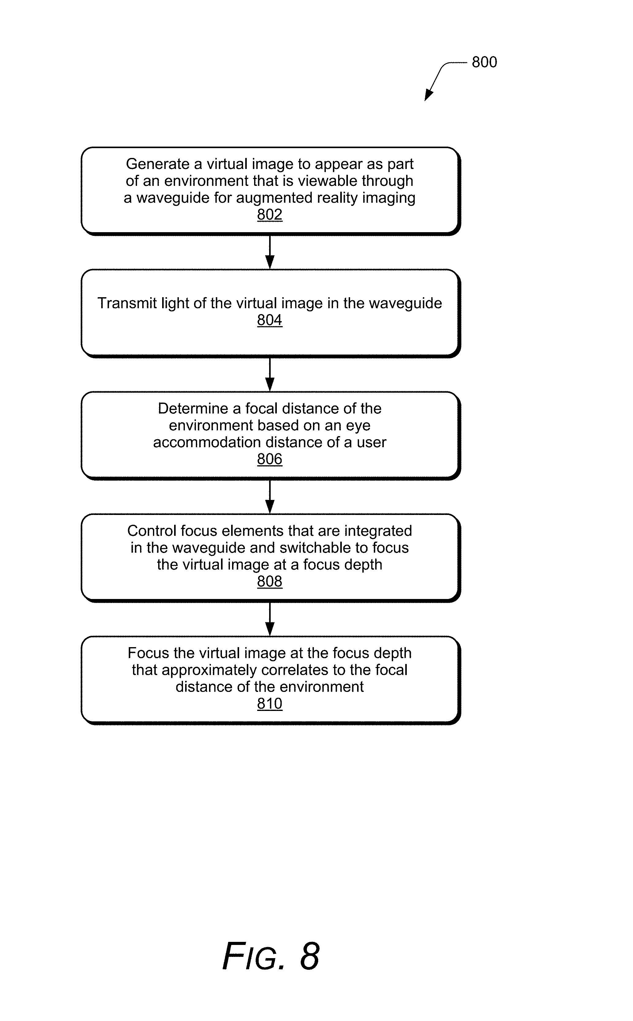
Waveguide optics focus elements are described. In embodiments, an imaging structure includes a waveguide for viewing of an environment that is viewable with the imaging structure. The waveguide combines light of a virtual image with the transmitted light of the environment so that the virtual image appears as part of the environment for augmented-reality imaging or virtual-reality imaging. The imaging structure also includes one or more focus elements that are integrated in the waveguide and switchable to focus the virtual image at a focus depth that approximately correlates to a focal distance of the environment. The focus elements can each be implemented for a different focus depth of the virtual image, and the focus depth is adjustable based on a combination of the focus elements being switched-on or switched-off.
In other embodiments, the focus elements that are integrated in the waveguide can be implemented as switchable output reflective devices or switchable output diffractive devices, such as Switchable Bragg Gratings. For example, a first switchable output diffractive device is implemented to focus the virtual image at infinity when switched-on, yet allow light to continue propagating down the waveguide when switched-off. This first switchable output diffractive device has simple wedge power to diffract light that is propagating in the waveguide into a direction that can be viewed by a user. A second switchable output diffractive device is implemented to focus the virtual image at an intermediate focus depth when switched-on, yet allow light to continue propagating down the waveguide when switched-off. The diffractive power of this second switchable output diffractive device is a combination of wedge power and lens power. A third switchable output diffractive device is implemented to focus the virtual image at a near focus depth when switched-on, yet allow light to continue propagating down the waveguide when switched-off. The diffractive power of the third switchable output diffractive device is a combination of wedge power and lens power, and the lens power of this third device is greater than the lens power of the second switchable output diffractive device.
BRIEF DESCRIPTION OF THE DRAWINGS
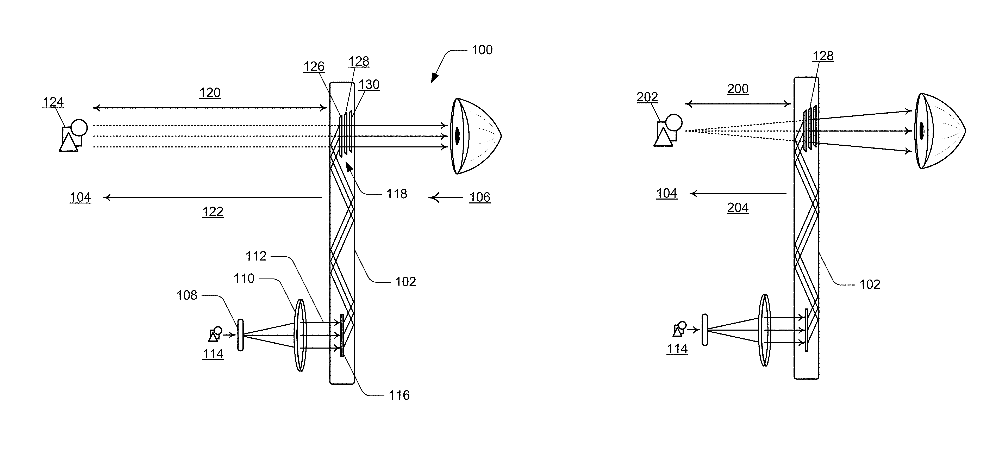
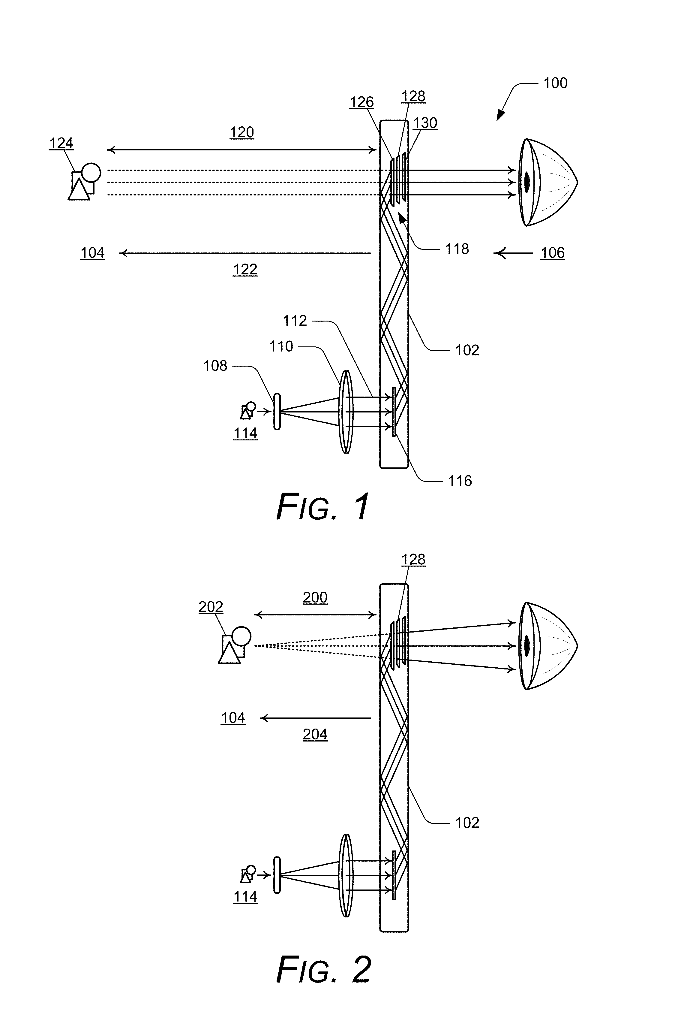
Embodiments of waveguide optics focus elements are described with reference to the following Figures. The same numbers may be used throughout to reference like features and components that are shown in the Figures:
FIG. 1 illustrates an example imaging structure in accordance with one or more embodiments of waveguide optics focus elements.
FIGS. 2 and 3 further illustrate the example imaging structure shown in FIG. 1 in accordance with one or more embodiments of waveguide optics focus elements.
FIG. 4 illustrates another example imaging structure in accordance with one or more embodiments of waveguide optics focus elements.
FIG. 5 illustrates another example imaging structure in accordance with one or more embodiments of waveguide optics focus elements.
FIG. 6 illustrates an example system that includes examples of imaging units in which embodiments of waveguide optics focus elements can be implemented.
FIG. 7 illustrates an example system that includes an example of a wearable display device in which embodiments of waveguide optics focus elements can be implemented.
FIG. 8 illustrates example method(s) of waveguide optics focus elements in accordance with one or more embodiments.
FIG. 9 illustrates various components of an example device that can implement embodiments of waveguide optics focus elements.
DETAILED DESCRIPTION
Embodiments of waveguide optics focus elements are described. An imaging structure can be implemented with focus elements that are switchable to focus a virtual image at a focus depth that approximately correlates to a focal distance of an environment that is viewed through the imaging structure. For augmented reality imaging and/or virtual reality imaging, virtual objects and/or images that appear closer than infinity (e.g., at a close focus distance) is an improvement over displays that are based at infinity focus. Embodiments of waveguide optics focus elements can be implemented for wearable display devices, hand-held augmented reality displays, and larger format displays, such as vehicle head up displays or even for larger architectural displays. Embodiments of waveguide optics focus elements are also applicable for non-see-through displays of any size and configuration that provide a user with a virtual image at some viewing distance other than the distance of the user's eyes to the display device.
In embodiments, waveguide optics focus elements provides focus accommodation with no power, lens power, wedge power, or a combination of lens power and wedge power. Lens power can be added to the input diffraction element of a waveguide display, which reduces the number of lenses in a system. Lens power can also be added to the output diffractive element of a waveguide display. Switchable diffractive devices, such as Switchable Bragg Gratings (SBGs), can be implemented for focus accommodation so that the focal depth of a virtual image appears at approximately the same focal distance as an object or image that is viewed in an environment over which the virtual image is projected.
While features and concepts of waveguide optics focus elements can be implemented in any number of different devices, systems, environments, and/or configurations, embodiments of waveguide optics focus elements are described in the context of the following example devices, systems, and methods.
FIG. 1 illustrates an example imaging structure 100 that includes waveguide optics focus elements in accordance with embodiments described herein. The imaging structure 100 includes a waveguide 102 for see-through viewing of an environment 104 that is viewable through the imaging structure, such as for a user viewing the environment from a perspective 106. The imaging structure also includes an image microdisplay 108 and an imaging optic 110 that implement an input mechanism to direct the light 112 of a generated, virtual image 114 into the waveguide where the light of the virtual image is then reflected through the waveguide. The image microdisplay 108 can be implemented as a liquid crystal on silicon (LCOS) microdisplay that projects the virtual image through the imaging optic 110 into the waveguide, or implemented for any other type and size of display device.
In embodiments, the imaging structure 100 can be implemented in an imaging unit of a head-mounted display (HMD), such as glasses or other type of wearable display device, hand-held display, or larger format display such as a vehicle head up display. An imaging unit that incorporates the imaging structure 100 can generate the virtual image 114 to appear as part of the environment 104 for augmented-reality imaging and/or viewing. Waveguide optics-based displays can be implemented to collimate light and then direct the light into the waveguide 102 by diffractive or reflective components, such as any type of optics, lenses, or other light-directing mechanisms. The components for extracting light out of the waveguide and projecting the light of an image for viewing can also be diffractive or reflective. Generally the diffractive or reflective components for in-coupling and out-coupling have a simple wedge power (also referred to as prismatic power). Additionally, the diffractive or reflective components can be implemented with a component of lens power for both lens power and prismatic power.
In implementations, the input mechanism (e.g., the image microdisplay 108 and imaging optic 110) can include a lens power for the two functions of collimating the light and injecting the light into the waveguide 102. This can be implemented with a diffractive device. Additionally, the input mechanism may be combined with other lenses and/or optics components. For example, the waveguide 102 of the imaging structure 100 may also include an input grating 116 to add diffractive power at the input of the light to the waveguide. At the light output of the waveguide 102, an output mechanism may be implemented for less lens power so that a displayed virtual image appears closer than infinity in the environment, as viewed through the imaging structure.
The wedge power of the waveguide normal output grating and the diffractive power of a lens can be combined in a waveguide display. Generally, the diffraction efficiency of diffractive surfaces is less than 100%, and some of the light passes directly through the diffractive surface. For example, some of the light that is propagating in a waveguide and that is not diffracted will continue down the waveguide until it hits the diffractive surface again. Some of the light will be diffracted out of the waveguide and some of the light will continue propagating down the waveguide. For waveguide displays, the light output at the exit pupil can be expanded so that the input beam of light is much smaller than the exiting light. For an output diffractive surface that has lens power, the light will be diffracted out of the waveguide in the correct direction for that part of the diffractive lens (and the input beam of light can still be smaller than the output lens size).
In embodiments of waveguide optics focus elements as described herein, the waveguide 102 includes focus elements 118 that are integrated in the waveguide and are switchable on and off to focus the virtual image 114 at a focus depth 120 that approximately correlates to a focal distance 122 of the environment 104. The virtual image 114 is also shown displayed as the focused virtual image 124 at the focus depth 120. In this example, three focus elements 118 (e.g., switchable output diffractive devices) are integrated in the waveguide 102 and each is implemented for a different focus depth of the virtual image. For example, a first focus element 126 is implemented to focus the virtual image 114 at infinity (e.g., as the focused virtual image 124) when switched-on, yet allow the light 112 to continue propagating down the waveguide when switched-off. In alternate implementations, any of the focus elements may be implemented to switch-off to focus the virtual image and switch-on to allow the light to continue propagating down the waveguide, or may be implemented to switch-in and/or switch-out.
A second focus element 128 is implemented to focus the virtual image 114 at an intermediate focus depth 200 (e.g., as the focused virtual image 202 shown in FIG. 2) when switched-on, yet allow the light to continue propagating down the waveguide when switched-off. The second focus element 128 focuses the virtual image at the intermediate focus depth 200 that approximately correlates to a focal distance 204 of the environment 104. A third focus element 130 is implemented to focus the virtual image 114 at a near focus depth 300 (e.g., as the focused virtual image 302 shown in FIG. 3) when switched-on, yet allow the light to continue propagating down the waveguide when switched-off. The third focus element 130 focuses the virtual image at the near focus depth 300 that approximately correlates to a focal distance 304 of the environment 104.
Although the imaging structure 100 that is shown and described in this example includes the three focus elements 118, the waveguide 102 can be implemented with any number of focus elements in other embodiments. For example, the waveguide may include only one focus element, or more than three focus elements, depending on the number of discrete focus levels that are implemented. In implementations, three or four discrete focus levels may adequately accommodate user depth of field for augmented reality imaging. The number of focus elements that are implemented can be selectively switched-on and/or switched-off, or may be implemented to switch-in and/or switch-out, to change or adjust the focus depth of a displayed virtual image.
The focus elements 118 can be implemented as switchable output diffractive devices, such as Switchable Bragg Gratings (SBGs), as switchable output reflective devices, or as any type of active device, such as polymer liquid crystal devices. Switchable Bragg Gratings are manufactured by SBG Labs and are described as having sub-millisecond switching speeds providing a high diffraction efficiency when activated, as well as optical transparency when inactive. The multiple focus elements 118 implemented as SBGs provide several focal distances for the imaging structure 100. The SBGs utilize Holographic Polymer-Dispersed Liquid Crystals and when switched-off, the refractive index of the liquid crystal approximately matches that of the surrounding polymer of the waveguide so that the SBG is essentially transparent to the display light. When an SBG is switched-on, the liquid crystal has a different refractive index than the polymer of the waveguide. An SBG is also a holographic device and the spectral bandwidth is very limited, so that the light of the environment image (the real image) is not affected (or very little) by the focusing device. Accordingly, the environment can be focused as normal, and the light of the virtual image overlaid on top of the environment light for augmented reality imaging.
In embodiments, a wearable display device that incorporates the imaging structure 100, such as the example wearable display device as described with reference to FIG. 7, can include eye-tracking cameras used to determine user pupil locations and to track eye movements. Additionally, a wearable display device may include other sensors, such as head tracking, world recognition, and/or proximity sensors that can be used to determine the eye accommodation distance of the user (also referred to herein as focus adjust). A wearable display device can also include a controller and/or an imaging application, such as a software application, to implement embodiments of waveguide optics focus elements as described herein. The imaging application can receive focus adjust data, such as eye-tracking data and/or other sensor data, and determine the focal distance of the environment based on the focus adjust data that indicates the eye accommodation distance of a user. The imaging application is also implemented to initiate focus control signals to control a combination of the focus elements 118 being switched-on or switched-off to adjust the focus depth of the virtual image.
For example, the first focus element 126 is implemented to focus the virtual image 114 at infinity (e.g., as the focused virtual image 124) when switched-on and when the second and third focus elements are switched-off. The second focus element 128 is implemented to focus the virtual image 114 at an intermediate focus depth 200 (e.g., as the focused virtual image 202 shown in FIG. 2) when switched-on and when the first and third focus elements are switched-off. The third focus element 130 is implemented to focus the virtual image 114 at a near focus depth 300 (e.g., as the focused virtual image 302 shown in FIG. 3) when switched-on and the second and third focus elements are switched-off. In alternate embodiments, more than one of the focus elements 118 may be switched-on to focus the virtual image at a desired focus depth. Multiple combinations of the diffractive devices may be used to provide a larger range and increased number of focus settings, whereby the secondary focus elements can be used to fine tune the focus distance.
FIG. 2 further illustrates the example imaging structure 100 that is shown and described with reference to FIG. 1. As described above, the focus element 128 in the waveguide 102 is implemented to focus the virtual image 114 at an intermediate focus depth 200 as the focused virtual image 202 when switched-on, and diffract the light of the virtual image when switched-off. The intermediate focus depth 200 is representative of any focus depth between infinity (e.g., the focus depth 120 shown in FIG. 1) and the near focus depth 300 shown in FIG. 3.
FIG. 3 further illustrates the example imaging structure 100 that is shown and described with reference to FIG. 1. As described above, the focus element 130 in the waveguide 102 is implemented to focus the virtual image 114 at a near focus depth 300 as the focused virtual image 302 when switched-on, and diffract the light of the virtual image when switched-off.
FIG. 4 illustrates an alternate example of an imaging structure 400 that can be implemented with waveguide optics focus elements in accordance with embodiments described herein. As generally described with reference to FIG. 1, the imaging structure 400 includes a waveguide 402 for see-through viewing of an environment 404 that is viewable through the imaging structure, such as for a user viewing the environment from a perspective 406. The imaging structure also includes an image microdisplay 408 and an imaging optic 410 that implement an input mechanism to direct the light 412 of a generated, virtual image 414 into the waveguide where the light of the virtual image is then reflected through the waveguide. Optionally, the waveguide of the imaging structure 400 may also include an input grating 416 to add diffractive power at the input of the light to the waveguide.
In embodiments of waveguide optics focus elements as described herein, the waveguide 402 includes focus elements 418 that are switchable on and off to focus the virtual image 414 at a focus depth 420 that approximately correlates to a focal distance 422 of the environment 404. The virtual image 414 is also shown displayed as the focused virtual image 424 at the focus depth 420. In this example imaging structure 400, a first focus element 426 is integrated in the waveguide. Additional focus elements 428 and 430 are implemented outside of the waveguide 402 so that the output switchable diffractive surfaces of wedge power and lens power are separated. The first focus element 426 that is integrated in the waveguide is implemented to focus the virtual image 414 at infinity as the focused virtual image 424. The secondary focus elements 428 and 430 can be utilized to implement lens power for the imaging structure.
In this configuration of the example imaging structure 400, the diffraction efficiency may not be 100%, which may result in a ghost image 432 that is generated by light passing through the diffractive lens in the zero order (un-diffracted state). For example, most of the exit light will be directed into the intended focus element 428, but there may be some of the light that exits through the first focus element 426 at focus infinity to create the ghost image 432. In implementations, focus elements that have an improved diffraction efficiency so as not to create a ghost image may be implemented in this configuration of the example imaging structure 400. In embodiments, the example imaging structure 100 with the integrated focus elements 118 may be a preferable implementation because the light that does not get diffracted out of the waveguide continues to propagate within the waveguide rather than projecting a ghost image.
FIG. 5 illustrates another alternate example of an imaging structure 500 that can be implemented with waveguide optics focus elements in accordance with embodiments described herein. As generally described with reference to FIG. 1, the imaging structure 500 includes a waveguide 502 for see-through viewing of an environment 504 that is viewable through the imaging structure, such as for a user viewing the environment from a perspective 506. The imaging structure also includes an image microdisplay 508 and an imaging optic 510 that implement an input mechanism to direct the light 512 of a generated, virtual image 514 into the waveguide where the light of the virtual image is then reflected through the waveguide. Optionally, the waveguide of the imaging structure 500 may also include an input grating 516 to add diffractive power at the input of the light to the waveguide.
In embodiments of waveguide optics focus elements as described herein, the waveguide 502 includes focus elements 518 that are switchable on and off to focus the virtual image 514 at a focus depth 520 that approximately correlates to a focal distance 522 of the environment 504. The virtual image 514 is also shown displayed as the focused virtual image 524 at the focus depth 520. In this example imaging structure 500, a first focus element 526 is integrated in the waveguide. Additional focus elements 528 and 530 are implemented outside of the waveguide 502 so that the output switchable diffractive surfaces of wedge power and lens power are separated. The first focus element 526 that is integrated in the waveguide is implemented to focus the virtual image 514 at infinity as the focused virtual image 524. The secondary focus element 528 can be utilized to implement lens power for the imaging structure.
In this configuration of the example imaging structure 500, the focus element 530 is implemented as two switchable output diffractive devices, such as Switchable Bragg Gratings (SBGs), positioned back-to-back. This configuration forms a transmissive holographic lens that provides a combination of prismatic power and lens power outside of the waveguide. If implemented for a low wedge power, then the diffraction efficiency will also be low and the back-to-back configuration cancels the chromatic dispersion that may generate the ghost image as described with reference to FIG. 4.
FIG. 6 illustrates an example system 600 in which various embodiments of waveguide optics focus elements can be implemented. An example wearable display device 602 includes left and right display lens systems with imaging units, such as imaging units 604 that are viewed from a perspective 606 of the wearable display device, as if viewing the display lens systems from the top of the device. In embodiments, the imaging units 604 can be implemented as left and right display lens systems of the wearable display device described with reference to FIG. 7. A wearable display device can be implemented as any type of glasses or head-mounted display (HMD) that includes implementations of the imaging units 604 (e.g., left and right display lens systems) through which a user can view the surrounding environment, yet also see virtual images that are generated for display and appear as a part of the environment. References to a left imaging unit and a right imaging unit, as described herein, correlate to a user's left and right eyes (e.g., from the perspective of wearing and looking through the wearable display device). Alternatively, the left and right imaging units may be described from the perspective of looking at the wearable display device.
The imaging units 604 include examples of the imaging structure 100 as shown and described with reference to FIGS. 1-3. For example, the imaging units include the waveguide 102 with the focus elements 118, as well as the input mechanism (e.g., the image microdisplay 108 and imaging optic 110) to direct the light of a virtual image into the waveguide where the light of the virtual image is then reflected through the waveguide. In this example, the imaging units 604 can be implemented with any number of micro display panels, imaging structures with direct emitters, lenses, and reflecting elements to display and project a virtual image into a see-through and reflecting waveguide. Alternatively, the imaging units 604 can be implemented with the example imaging structures 400 or 500 described with reference to respective FIGS. 4 and 5, or with other imaging unit configurations.
The see-through, reflecting waveguide 102 is a display optic implemented for internal reflection and conducts visible light of a virtual image that is generated by the imaging units 604 and projected for viewing by a user. The waveguide 102 also passes through light 608 of an image from the surrounding environment for viewing by the user (e.g., an image of the environment as viewed through the wearable display device). An imaging unit 604 with an imaging structure can also be implemented with components of the display lens system described with reference to FIG. 7 to implement embodiments of waveguide optics focus elements.
In embodiments, the imaging units 604 each include a printed circuit board 610 that incorporates an emitter structure 612, which direct emits the light that is reflected by a reflecting mirror 614 to illuminate the image microdisplay 108. The imaged light is then directed through the imaging optic 110 that directs the light into the waveguide 102. The emitter structure 612 can be implemented with lasers that direct emit the light, and a reflective spatial light modulator can be implemented as the microdisplay using the lasers for illumination.
FIG. 7 illustrates an example system 700 that includes an example wearable display device 702 in which embodiments of waveguide optics focus elements can be implemented. The wearable display device can be implemented as any type of glasses or head-mounted display (HMD) that includes display lens systems 704 (e.g., left and right display lens systems) through which a user can view the surrounding environment, yet also see virtual images (e.g., any type of object, video, text, graphic, and the like) that are generated for display and appear as a part of the environment.
The wearable display device 702 can be implemented as an independent, portable system that includes memory, software, a processor, and/or a power source. Alternatively or in addition, the wearable display device may be communicatively linked to a controller 706 that includes any one or combination of the memory, software, processor, and/or power source, such as a battery unit. The controller can be implemented for wired or wireless communication with the wearable display device. The controller and/or the wearable display device can also be implemented with any number and combination of differing components as further described with reference to the example device shown in FIG. 9. For example, the controller and/or the wearable display device includes an imaging application implemented as computer-executable instructions, such as a software application, and executed by a processor to implement embodiments of waveguide optics focus elements as described herein.
In embodiments, the controller may be implemented as a dedicated device (e.g., the wired controller 706), as a mobile phone 708, a tablet or other portable computer device, a gaming system 710, or as any other type of electronic device that can be implemented to process and generate virtual images for display as part of the environment that is viewed through the display lens system of the wearable display device. The controller may communicate with the wearable display device wirelessly via WiFi.TM., Bluetooth.TM., infrared (IR), RFID transmission, wireless Universal Serial Bus (WUSB), cellular, or via other wireless communication techniques.
The example system 700 also includes a data server 712, or data service, that communicates, or otherwise distributes, virtual image data 714 to the wearable display device 702 via a communication network 716. For example, the data server may be part of a network-based gaming system that generates virtual images for augmented reality display at the wearable display device. Alternatively, the data server may be part of a navigation system that communicates navigation directions and information for display in the display lens systems 704 of the wearable display device. In another example, the data server may be part of a messaging service, such as an e-mail or text messaging system, that communicates e-mail and/or text messages to the wearable display device for display in the display lens systems, where a user can read a message as an augmented reality image that is displayed over the environment viewed through the wearable display device.
Any of the devices, servers, and/or services can communicate via the communication network 716, which may be implemented to include wired and/or wireless networks. The communication network can also be implemented using any type of network topology and/or communication protocol, and can be represented or otherwise implemented as a combination of two or more networks, to include IP-based networks and/or the Internet. The communication network may also include mobile operator networks that are managed by mobile operators, such as a communication service provider, cell-phone provider, and/or Internet service provider.
The wearable display device 702 includes a frame 718, such as in the form of glasses, goggles, or any other structure, that supports and incorporates the various components of the device, as well as serves as a conduit for electrical and other component connections. A components module 720 (or components modules on the left, right, and/or both sides of the device frame) incorporates any of the various components, such as processing and control circuitry, memory, software, a processor, GPS transceiver, and/or power source. The wearable display device may also include a microphone 722 to record audio data from the surrounding environment, as well as ear phones for audio feedback as part of an augmented reality experience.
The wearable display device 702 also includes various cameras 724 that capture video and still images of the surrounding environment. The image and video data can be processed on the device and/or by a controller device (e.g., controller 706), and used to create a mapping field to orient and track a user in the environment space. The wearable display device can also include eye-tracking cameras used to determine a user eyeball and/or pupil location, and to track eye movements. The wearable display device may also include a temperature sensor, as well as inertial sensors and/or attitude sensors, including MEMS gyros, magnetic sensors (e.g., a compass), and acceleration sensors for sensing position, orientation, and acceleration of the wearable display device.
An example of one display lens system 704 is shown from a viewer perspective 726 of the wearable display device 702, as if viewing the display lens system from the top of the device. The display lens system includes an imaging system 728, which can be implemented with any number of micro display panels, lenses, and reflecting elements to display and project a virtual image into a see-through and reflecting waveguide 730. A display lens system 704 can also be implemented as the imaging units described with reference to FIG. 6 that incorporate any of the imaging structures described with reference to FIGS. 1-5 to implement embodiments of waveguide optics focus elements. The see-through, reflecting waveguide 730 is implemented for internal reflection and conducts the visible light 732 of a virtual image that is generated by the imaging unit for viewing by a user, and also passes through the light 734 from the surrounding environment for viewing by the user.
The micro display panels, lenses, and/or reflecting elements of the imaging system 728 can be implemented with various display technologies, such as implemented with a transparent LCD, or using a transmissive projection technology where the light source is modulated by optically active material, backlit with white light. These technologies can be implemented using LCD type displays with powerful backlights and high optical energy densities. Alternatively, a micro display and/or reflecting element can be implemented using a reflective technology, such as digital light processing (DLP) and liquid crystal on silicon (LCOS), that reflects external light, which is reflected and modulated by an optical material.
In embodiments, the imaging system 728 (or other components of a display lens system 704) can be implemented to include an infra-red (IR) laser utilized for system calibrations and/or as an illumination source for an eye-tracking system and camera that tracks the position of a user's eyes and/or pupils. The eye-tracking system includes the eye-tracking illumination source, which is not a visible light, and includes an eye-tracking IR sensor. The IR sensor can be implemented as an IR camera that provides infrared image data of the eye for eye-tracking processing, or an IR sensor that detects eye reflections when the eye is illuminated. Alternatively or in addition, sensors can be implemented in a CMOS driver array to detect the feedback. In implementations, the light reflections (e.g., the IR return) may be directed with SBG or SRB methods. The see-through and reflecting waveguide 730 can also be utilized for the infrared illumination, and for eyeball reflections that the eye-tracking system uses to track the position of the user's eyes and/or pupils.
In this example, the display lens systems 704 include an optional opacity filter 736, and a see-through lens 738 on each side of the waveguide 730. The see-through lenses can be standard eye-glass lenses and made to prescription (or no prescription). The opacity filter selectively blocks natural light, either uniformly or on a per-pixel basis, from passing through the see-through and reflecting waveguide to enhance the contrast of a displayed virtual image.
Example method 800 is described with reference to FIG. 8 in accordance with one or more embodiments of waveguide optics focus elements. Generally, any of the services, functions, methods, procedures, components, and modules described herein can be implemented using software, firmware, hardware (e.g., fixed logic circuitry), manual processing, or any combination thereof. A software implementation represents program code that performs specified tasks when executed by a computer processor. The example methods may be described in the general context of computer-executable instructions, which can include software, applications, routines, programs, objects, components, data structures, procedures, modules, functions, and the like. The program code can be stored in one or more computer-readable storage media devices, both local and/or remote to a computer processor. The methods may also be practiced in a distributed computing environment by multiple computer devices. Further, the features described herein are platform-independent and can be implemented on a variety of computing platforms having a variety of processors.
FIG. 8 illustrates example method(s) 800 of waveguide optics focus elements. The order in which the method blocks are described are not intended to be construed as a limitation, and any number of the described method blocks can be combined in any order to implement a method, or an alternate method.
At block 802, a virtual image is generated to appear as part of an environment that is viewable through a waveguide for augmented reality imaging. For example, an imaging unit 604 (FIG. 6) that incorporates the example imaging structure 100 (FIG. 1) generates the virtual image 114 to appear as the focused virtual image 124 in the environment 104 that is viewable through the waveguide 102 for augmented reality imaging.
At block 804, light of the virtual image is transmitted in the waveguide. For example, the image microdisplay 108 and imaging optic 110 that implement the input mechanism direct the light 112 of the generated, virtual image 114 into the waveguide 102 where the light of the virtual image is then transmitted through the waveguide.
At block 806, a focal distance of the environment is determined based on an eye accommodation distance of a user. For example, the eye accommodation distance (or focal view) of the user can be based on eye-tracking, such as implemented with the wearable display device 702 (FIG. 7) that includes eye-tracking cameras used to determine user pupil locations and to track eye movements. Alternatively or in addition, the eye accommodation distance of the user (also referred to herein as focus adjust) may be determined by the type of content being displayed, or the focus adjust can be determined by other sensors on the wearable display device, such as head tracking, world recognition, and/or proximity sensors. The wearable display device also includes an imaging application 928 (FIG. 9), such as a software application, that receives focus adjust data and determines the focal distance 122 of the environment 104 based on the focus adjust data that indicates the focal view of a user.
At block 808, focus elements that are integrated in the waveguide and switchable to focus the virtual image at a focus depth are controlled. For example, the imaging application 928 controls the focus elements 118 that are integrated in the waveguide 102. The focus elements are each implemented for a different focus depth of the virtual image and are switchable on and off to focus the virtual image 114 at a focus depth. The focus elements can be implemented as switchable output reflective devices or switchable output diffractive devices, such as the Switchable Bragg Gratings (SBGs) described above.
At block 810, the virtual image is focused at the focus depth that approximately correlates to the focal distance of the environment. For example, the first focus element 126 focuses the virtual image 114 at infinity as the focused virtual image 124. The second focus element 128 focuses the virtual image 114 at an intermediate focus depth 200 as the focused virtual image 202. The second focus element 128 focuses the virtual image at the intermediate focus depth 200 that approximately correlates to a focal distance 204 of the environment 104. The third focus element 130 focuses the virtual image 114 at a near focus depth 300 as the focused virtual image 302. The third focus element 130 focuses the virtual image at the near focus depth 300 that approximately correlates to a focal distance 304 of the environment 104. In embodiments, the focus depth of the virtual image is adjusted based on a combination of the focus elements switched-on or switched-off. In alternate embodiments, more than one of the focus elements 118 may be switched-on to focus the virtual image at a desired focus depth. Multiple combinations of the diffractive devices may be used to provide a larger range and increased number of focus settings, whereby the secondary focus elements can be used to fine tune the focus distance.
FIG. 9 illustrates various components of an example device 900 that can be implemented as any of the devices described with reference to the previous FIGS. 1-8, such as a wearable display device and/or a controller for a wearable display device. In embodiments, the device may be implemented as any one or combination of a fixed or mobile device, in any form of a consumer, computer, portable, communication, phone, navigation, appliance, gaming, media playback, and/or electronic device. The device may also be associated with a user (i.e., a person) and/or an entity that operates the device such that a device describes logical devices that include users, software, firmware, hardware, and/or a combination of devices.
The device 900 includes communication devices 902 that enable wired and/or wireless communication of device data 904, such as virtual image data, as well as video and images data, and other media content stored on the device. The media content stored on the device can include any type of audio, video, and/or image data. The device includes one or more data inputs 906 via which any type of data, media content, and/or inputs can be received, such as user-selectable inputs and any other type of audio, video, and/or image data received from any content and/or data source. The data inputs 906 may include USB ports, coaxial cable, and other serial or parallel connectors (including internal connectors) for flash memory, DVDs, CDs, and the like. The data inputs can be used to couple the device to components, peripherals, and accessories, such as keyboards, microphones, cameras, and any other type of input devices.
The device 900 also includes communication interfaces 908, such as any one or more of a serial, parallel, network, or wireless interface. The communication interfaces provide a connection and/or communication links between the device and a communication network by which other electronic, computing, and communication devices communicate data with the device. Although not shown, the device can include a system bus or data transfer system that couples the various components within the device. A system bus can include any one or combination of different bus structures, such as a memory bus or memory controller, a peripheral bus, a universal serial bus, and/or a processor or local bus that utilizes any of a variety of bus architectures.
The device 900 includes one or more processors 910 (e.g., any of microprocessors, controllers, and the like), or a processor and memory system (e.g., implemented in an SoC), which process computer-executable instructions to control the operation of the device. Alternatively or in addition, the device can be implemented with any one or combination of software, hardware, firmware, or fixed logic circuitry that is implemented in connection with processing and control circuits which are generally identified at 912.
The device 900 also includes one or more memory devices 914 (e.g., computer-readable storage media) that enable data storage, such as random access memory (RAM), non-volatile memory (e.g., read-only memory (ROM), flash memory, etc.), and a disk storage device. A disk storage device may be implemented as any type of magnetic or optical storage device, such as a hard disk drive, a recordable and/or rewriteable disc, and the like. The device may also include a mass storage media device. Computer-readable storage media can be any available medium or media that is accessed by a computing device.
A memory device 914 provides data storage mechanisms to store the device data 904, sensor data 916 from calibration sensors 918, focus adjust data 920 from cameras 922 and/or from the sensors 918, other types of information and/or data, and device applications 924. For example, an operating system 926 can be maintained as a software application with the memory device and executed on the processors. The device applications may also include a device manager or controller, such as any form of a control application, software application, signal processing and control module, code that is native to a particular device, a hardware abstraction layer for a particular device, and so on. In this example, the device applications also include an imaging application 928 that can implement embodiments of waveguide optics focus elements as described herein.
The device 900 may also include an audio and/or video processing system 930 that generates audio data for an audio system 932 and/or generates display data for a display system 934. The audio system and/or the display system may include any devices that process, display, and/or otherwise render audio, video, display, and/or image data. In implementations, the audio system and/or the display system are external components to the device. Alternatively, the audio system and/or the display system are integrated components of the example device.
Although embodiments of waveguide optics focus elements have been described in language specific to features and/or methods, the appended claims are not necessarily limited to the specific features or methods described. Rather, the specific features and methods are disclosed as example implementations of waveguide optics focus elements.
* * * * *
References
-
pnas.org/content/103/16/6100.long
-
optigrate.com/BragGrate_Mirror.html
-
digilens.com/products.html
-
defense-update.com/products/h/HDTV-HMD.htm
-
ciri.org.nz/downloads/Lightpipe%20design.pdf
-
gajitz.com/two-faced-transparent-phone-with-dual-touch-screens
-
nanolab.uc.edu/Publications/PDFfiles/355.pdf
-
citeseerx.ist.psu.edu/viewdoc/download?doi=10.1.1.33.4027&rep=rep1&type=pdf
-
empf.org/empfasis/2009/Oct09/cots.html
-
-
tweaktown.com/reviews/2733/twintech_geforce_gts_250_xt_oc_1gb_graphics_card/index3.html
-
ieeexplore.ieee.org/stamp/stamp.jsp?tp=&arnumber=926823
-
spie.org/documents/Newsroom/Imported/003805/003805_10.pdf
-
www2.electronicproducts.com/Selecting_displaybacklighting_for_portable_handheld_devices-article-farcglobal-feb2008-html.aspx
-
blog.laptopmag.com/first-transparent-tablet
-
lumamed.com/documents/5_polarized%20light%20imaging.pdf
-
intraweb.stockton.edu/eyos/energy_studies/content/docs/FINAL_PRESENTATIONS/4b-6%20.pdf
-
psilab.ucsd.edu/research/slab_concentration/files/SPIE_Slab_Published.pdf
-
proceedings.spiedigitallibrary.org
-
spiedl.org/terms
-
-
download.microsoft.com/download/D/2/E/D2E425F8-CF3C-4C71-A4A2-70F9D4081007/ParallelOpticsinWaveguideDisplaysMS090925.Final.pdf
-
-
ecma-international.org/activities/Acoustics/Inter-noise%202008%20paper%20on%20ECMA-74%20updates.pdf
-
oatao.univ-toulouse.fr/2874
-
-
-
research.microsoft.com/pubs/135609/reartype%20mobilehci.pdf
-
-
-
-
-
-
ijvr.org/issues/issue2-2010/paper1%20.pdf
-
pro-clockers.com/cooling/66-thermalright-ultra-120-extreme-cpu-cooler.html
-
dl.acm.org/citation.cfm?id=1294259
D00000
D00001
D00002
D00003
D00004
D00005
D00006
D00007
XML
uspto.report is an independent third-party trademark research tool that is not affiliated, endorsed, or sponsored by the United States Patent and Trademark Office (USPTO) or any other governmental organization. The information provided by uspto.report is based on publicly available data at the time of writing and is intended for informational purposes only.
While we strive to provide accurate and up-to-date information, we do not guarantee the accuracy, completeness, reliability, or suitability of the information displayed on this site. The use of this site is at your own risk. Any reliance you place on such information is therefore strictly at your own risk.
All official trademark data, including owner information, should be verified by visiting the official USPTO website at www.uspto.gov. This site is not intended to replace professional legal advice and should not be used as a substitute for consulting with a legal professional who is knowledgeable about trademark law.