Emitter with M-PAM modulation for wireless optical communication system
Maret , et al. De
U.S. patent number 10,498,455 [Application Number 16/006,190] was granted by the patent office on 2019-12-03 for emitter with m-pam modulation for wireless optical communication system. This patent grant is currently assigned to COMMISSARIAT A L'ENERGIE ATOMIQUE ET AUX ENERGIES ALTERNATIVES. The grantee listed for this patent is COMMISSARIAT A L'ENERGIE ATOMIQUE ET AUX ENERGIES ALTERNATIVES. Invention is credited to Marc Laugeois, Luc Maret, Xavier Popon.


| United States Patent | 10,498,455 |
| Maret , et al. | December 3, 2019 |
Emitter with M-PAM modulation for wireless optical communication system
Abstract
This invention relates to an emitter for an optical communication system such as a Li-Fi system. This emitter comprises an M-PAM modulator and a conversion module to convert an M-PAM symbol into a plurality of logical outputs. It also comprises a plurality of branches in parallel, each branch comprising a switched current source mounted in series with the optical source, each switched current source being controlled by a logical output from the conversion module.
| Inventors: | Maret; Luc (Polienas, FR), Laugeois; Marc (Grenoble, FR), Popon; Xavier (Seyssins, FR) | ||||||||||
|---|---|---|---|---|---|---|---|---|---|---|---|
| Applicant: |
|
||||||||||
| Assignee: | COMMISSARIAT A L'ENERGIE ATOMIQUE
ET AUX ENERGIES ALTERNATIVES (Paris, FR) |
||||||||||
| Family ID: | 59811494 | ||||||||||
| Appl. No.: | 16/006,190 | ||||||||||
| Filed: | June 12, 2018 |
Prior Publication Data
| Document Identifier | Publication Date | |
|---|---|---|
| US 20180359034 A1 | Dec 13, 2018 | |
Foreign Application Priority Data
| Jun 12, 2017 [FR] | 17 55219 | |||
| Current U.S. Class: | 1/1 |
| Current CPC Class: | H04B 10/5161 (20130101); H04B 10/502 (20130101); H04B 10/116 (20130101); H04B 10/114 (20130101); H04B 10/11 (20130101) |
| Current International Class: | H04B 10/11 (20130101); H04B 10/114 (20130101); H04B 10/50 (20130101); H04B 10/516 (20130101); H04B 10/116 (20130101) |
| Field of Search: | ;398/118-131,182-201 |
References Cited [Referenced By]
U.S. Patent Documents
| 6424444 | July 2002 | Kahn |
| 7546038 | June 2009 | Wang |
| 9882532 | January 2018 | Vera Villarroel |
| 9933639 | April 2018 | Lin |
| 10084619 | September 2018 | Dupuis |
| 2001/0035997 | November 2001 | Agazzi |
| 2004/0091270 | May 2004 | Choi |
| 2005/0147418 | July 2005 | Gurusami |
| 2008/0002988 | January 2008 | Cheng |
| 2012/0087677 | April 2012 | Jang |
| 2012/0173290 | July 2012 | Collins |
| 2012/0183290 | July 2012 | Schunk |
| 2013/0195464 | August 2013 | Fath |
| 2014/0255037 | September 2014 | Shang |
| 2014/0321864 | October 2014 | Bliss |
| 2015/0071651 | March 2015 | Asmanis |
| 2015/0263812 | September 2015 | Tatsumi |
| 2016/0062207 | March 2016 | Bai |
| 2016/0156417 | June 2016 | Tanaka |
| 2016/0164604 | June 2016 | Liu et al. |
| 2017/0025816 | January 2017 | Tanaka |
| 2018/0035498 | February 2018 | Rolindez Alberich |
| 2018/0069542 | March 2018 | Bonthron |
| 2018/0356654 | December 2018 | Tatsumi |
| 2019/0007141 | January 2019 | Kawata |
| 2019/0028204 | January 2019 | Nakamura |
| 103986516 | Aug 2014 | CN | |||
Other References
|
Quadir et al, A 56Gbs PAM 4 VCSEL driver circuit, Jun. 2012, ISSC, All Document. (Year: 2012). cited by examiner . Li et al, Design of 20 Gbs Four Level Pulse Amplitude Modulation VCSEL Driver in 90 nm CMOS Technology, Aug. 2016, IEEE, All Document. (Year: 2016). cited by examiner . Lu et al, A 56 Gbs PAM4 VCSEL Based LiFi Transmission With Two Stage Injection Locked Technique, Feb. 2017, IEEE, All Document. (Year: 2017). cited by examiner . French Preliminary Search Report dated Feb. 27, 2018 in French Application 17 55219 filed on Jun. 12, 2017 (with English Translation of Categories of Cited Documents). cited by applicant . Mohammed M. A. Mohammed, et al., "A Spectrally Efficient Unipolar PAM Single Carrier Frequency Domain Equalization for IM/DD Systems," IEEE, 2015, pp. 246-247. cited by applicant. |
Primary Examiner: Sanchez; Dibson J
Attorney, Agent or Firm: Oblon, McClelland, Maier & Neustadt, L.L.P.
Claims
The invention claimed is:
1. An emitter for an optical wireless communication system comprising: an M-PAM modulator configured to transform data to be transmitted into PAM (Pulse Amplitude Modulation) alphabet symbols with M levels in which M>2; an optical source configured to transmit said data; conversion circuitry configured to convert each M-PAM symbol into a plurality of logical outputs, using a conversion table; and a plurality of branches in parallel, each branch comprising a switched current source, mounted in series with the optical source, each switched current source being controlled by a logical output from the conversion circuitry, wherein the conversion circuitry is configured to convert each M-PAM symbol into a binary word with size .mu.=log.sub.2(M), and wherein outputs of the switched current sources are respectively equal to (I.sub.0, 2I.sub.0, . . . , 2.sup..mu.-1I.sub.0), in which I.sub.0 is a predetermined intensity value.
2. The emitter according to claim 1, wherein each of the branches is arranged in series between the optical source and ground, each branch comprising a transistor and a resistor in series, a gate of the transistor being connected to a corresponding logical output of the conversion circuitry.
3. The emitter according to claim 2, wherein a resistance of the resistor of each branch is determined to calibrate an output current of the respective switched current source.
4. The emitter according to claim 1, wherein each of the branches is arranged in series between the optical source and ground, each branch comprising a group of transistors in parallel and a resistor in series, and gates of said transistors in said group being connected to the same logical output of the conversion circuitry.
5. The emitter according to claim 1, wherein the optical wireless communication system is a Li-Fi system.
6. The emitter according to claim 5, wherein the optical source is a LED.
7. An emitter for an optical wireless communication system comprising: an M-PAM modulator configured to transform data to be transmitted into PAM (Pulse Amplitude Modulation) alphabet symbols with M levels in which M>2; an optical source configured to transmit said data; conversion circuitry configured to convert each M-PAM symbol into a plurality of logical outputs, using a conversion table; and a plurality of branches in parallel, each branch comprising a switched current source, mounted in series with the optical source, each switched current source being controlled by a logical output from the conversion circuitry, wherein the conversion circuitry is configured to convert each M-PAM symbol into a binary word with size .mu.=log.sub.2(M), and wherein an output of a switched current source connected to a logical output m=0, . . . , .mu.-1 of the conversion circuitry is chosen such that light power from the optical source is equal to 2.sup.m.PHI..sub.0 in which .PHI..sub.0 is a predetermined light power.
8. The emitter according to claim 7, wherein each of the branches is arranged in series between the optical source and ground, each branch comprising a transistor and a resistor in series, a gate of the transistor being connected to a corresponding logical output of the conversion circuitry.
9. The emitter according to claim 8, wherein a resistance of the resistor of each branch is determined to calibrate the light power from the optical source in series with the respective switched current source.
10. The emitter according to claim 7, wherein each of the branches is arranged in series between the optical source and ground, each branch comprising a group of transistors in parallel and a resistor in series, and gates of said transistors in said group being connected to the same logical output of the conversion circuitry.
11. The emitter according to claim 7, wherein the optical wireless communication system is a Li-Fi system.
12. The emitter according to claim 11, wherein the optical source is a LED.
Description
TECHNICAL DOMAIN
This invention relates to the domain of optical wireless communications in general, and particularly to Li-Fi (Light Fidelity) communication systems.
STATE OF PRIOR ART
A great deal of research has recently been made on Optical Wireless Communications (OWC) systems due to their ability to solve the spectral occupancy problem and to complement or even replace Wi-Fi systems.
Schematically, Li-Fi systems are analogous to Wi-Fi systems (respecting IEEE standard 802.11) but use the visible spectrum instead of the RF spectrum. The physical (PHY) layer and the MAC layer of Li-Fi systems have already been standardised in IEEE standard 802.15.7.
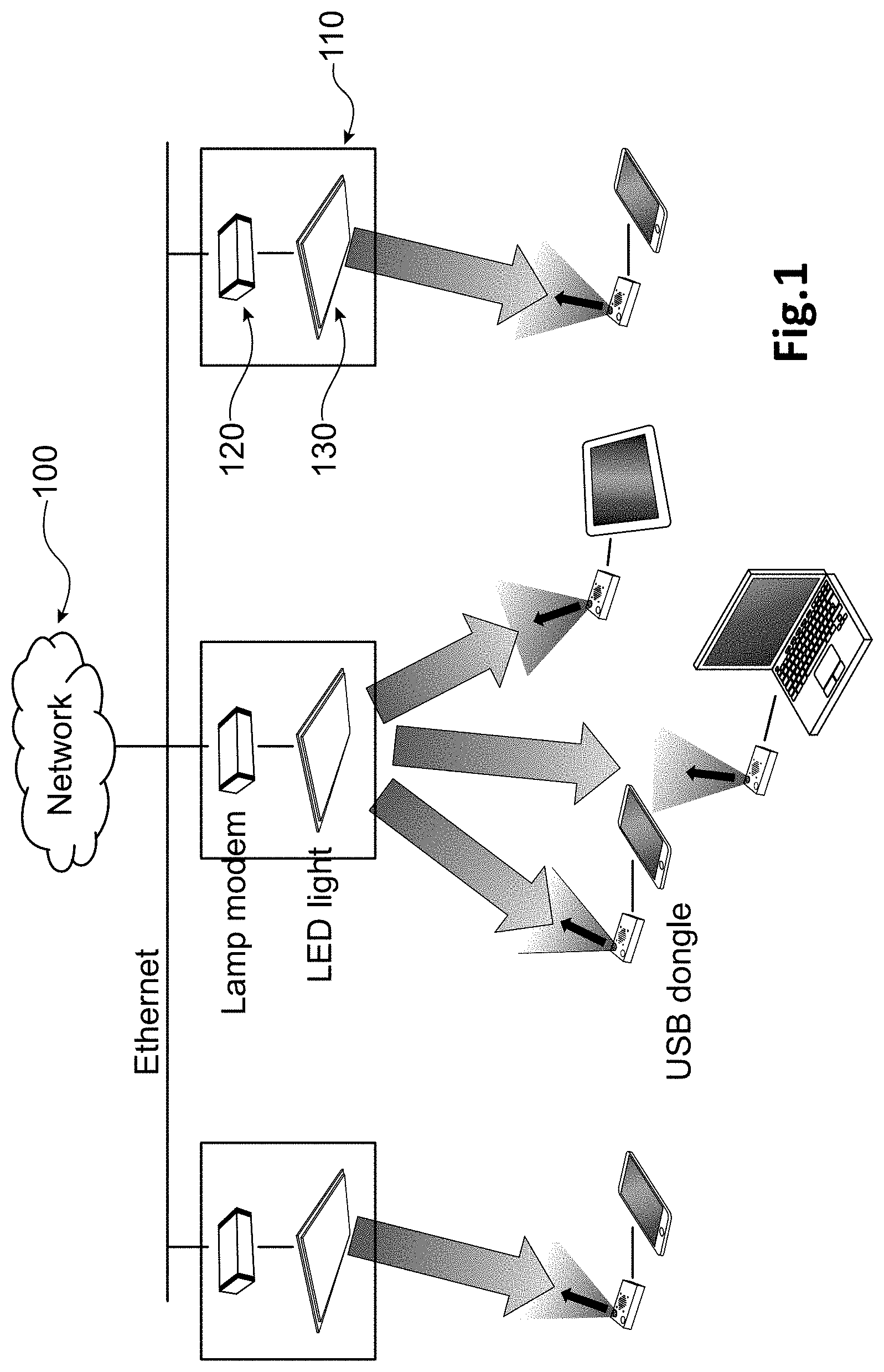
FIG. 1 diagrammatically represents an example of a Li-Fi system.
A plurality of light access points (APs) 110, are connected to the principal network 100 using Ethernet links. Each access point is composed of a modem 120 coupled to a LED light source 130 emitting in the visible range, the modem modulating the source power supply current so as to modulate the intensity of the light emitted. The terminals are equipped with a dongle including an optical receiver. This optical receiver receives the light signal, converts it into an electrical signal, demodulates it and recovers the transmitted data. Conversely, the dongle (or the terminal itself) is also equipped with an infrared diode. The data to be transmitted on the uplink then modulate the infrared signal. The infrared signal is received by a photodiode (not shown) mounted on the access point, and is then demodulated to transmit the data to the principal network (Ethernet or other network).
Modulation of optical signals on the uplink and on the downlink is a non-coherent modulation with direct detection at the receiver. Different types of modulation have been disclosed in the literature to take account of the real and single-pole nature of the light signal. Thus, the OOK (On Off Keying), PAM (Pulse Amplitude Modulation), PPM (Pulse Position Modulation), DCO-OFDM (Direct-Current Optical OFDM) and SIM-OFDM (Subcarrier Index Modulation OFDM) modulations have been envisaged.
In particular, the PAM modulation has been recommended on the uplink. Firstly, it has the advantage of reducing energy consumption of the terminal due to the lack of DC polarisation (in particular, unlike the DCO-OFDM modulation). It can then shift equalisation of the channel to the access point end. This equalisation is usually done in the frequency domain, which only requires the insertion of a cyclic prefix at the emitter end. Thus, the terminal calculation resources that can be relatively constrained, are not required. A communication system with M-PAM (PAM with M levels) modulation on emission and equalisation in the frequency domain on reception has thus been disclosed in the paper by M. M. A. Mohammed et al. entitled "A spectrally efficient unipolar PAM single-carrier frequency domain equalization for IM/DD systems" published in 2015 IEEE Proc. of Photonics Conf. (IPC), Reston, Va., pp. 246-247.
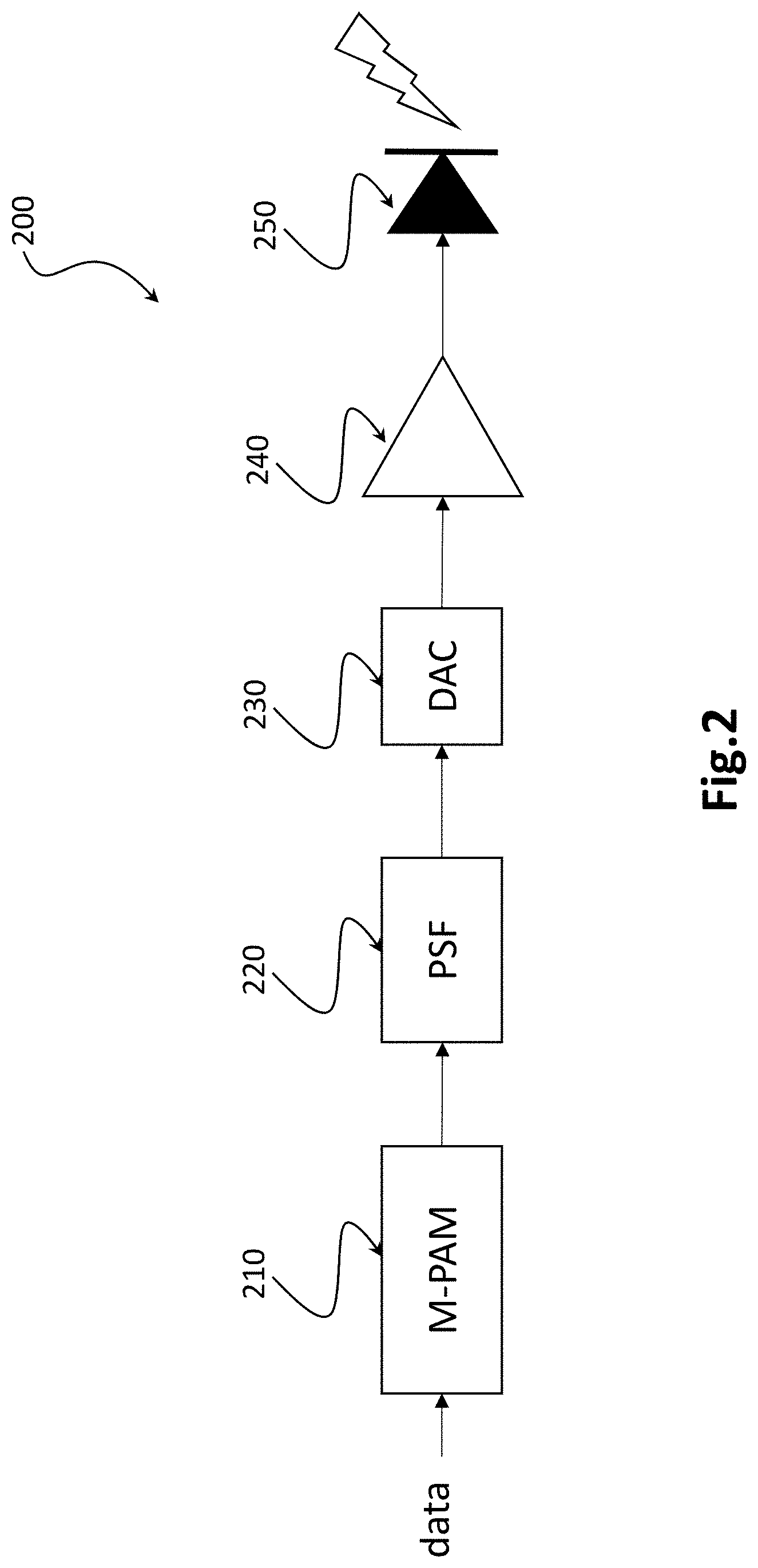
FIG. 2 diagrammatically represents the structure of an emitter with M-PAM modulation for an optical wireless telecommunication system.
Data to be emitted (binary words) are modulated by an M-PAM modulator (PAM with M levels), 210. The M-PAM symbols thus obtained are then filtered by a shaping filter 220 and are then converted into an analogue signal by a DAC 230. The purpose of shaping filtering is particularly to reduce interference between adjacent channels. The analogue signal is then amplified (in voltage or in current) by an amplifier 240 before controlling a LED source 250, for example an infrared LED source for the uplink and a white LED source (for example a blue LED with phosphor) for the downlink.
However, the emitter in FIG. 2 has the disadvantage that it requires a digital/analogue converter (DAC).
Patent application CN-A-103986516 describes an emitter of an optical communication system that eliminates the need for such a converter. Data to be transmitted are demultiplexed on a plurality of binary channels, each binary channel performing an OOK modulation (equivalent to a 2-PAM modulation) and switching a corresponding LED source in the visible range. The addition of optical signals at the photodiode emitted in parallel by the different LED sources can simulate an M-PAM modulation. However, this configuration has the disadvantage that it requires one LED source for each modulation level (M) and the emission from these different sources has to be synchronised. Furthermore, it does not function satisfactorily when the characteristics of channels being the different LED sources and the photodiode of the receiver are not identical.
Consequently, the purpose of this invention is to disclose an emitter for an optical communication system, and particularly for the uplink of a Li-Fi system, that is particularly simple and robust, particularly in that it does not require a set of LED sources nor a digital-analogue converter.
PRESENTATION OF THE INVENTION
This invention is defined by an emitter for an optical wireless communication system comprising an M-PAM modulator transforming data to be transmitted into PAM alphabet symbols with M levels in which M>2, and an optical source intended to transmit said data, said emitter comprising: a conversion module adapted to convert each M-PAM symbol into a plurality of logical outputs, using a biunivocal conversion table; a plurality of branches in parallel, each branch comprising a switched current source, mounted in series with the optical source, each switched current source being controlled by a logical output from the conversion module.
According to a first embodiment, the conversion module is adapted to convert each M-PAM symbol into a binary word with size M-1, the values of the intensities of switched current sources being identical (I.sub.0).
The conversion module is then adapted to convert each M-PAM symbol into a binary word comprising n bits in a first logical state and N-n bits in a complementary logical state, in which n is the level of the M PAM symbol.
Advantageously, the binary word is a thermometric code word.
According to a second embodiment, the conversion module is adapted to convert each M-PAM symbol into a binary word with size .mu.=log.sub.2(M), the intensities of switched current sources having values equal to (I.sub.0, 2I.sub.0, . . . , 2.sup..mu.-1I.sub.0), in which I.sub.0 is a predetermined intensity value.
According to a variant of the second embodiment, the conversion module is adapted to convert each M-PAM symbol into a binary word with size .mu.=log.sub.2(M), the intensity of the switched light source connected to the logical output m=0, . . . , .mu.-1 of the conversion module being chosen such that the light power from the optical source is equal to 2.sup.m.PHI..sub.0 in which .PHI..sub.0 is a predetermined light power.
According to a first configuration, each of the branches is arranged in series between the optical source and the ground, each branch comprising a transistor and a resistor in series, the transistor base being connected to a corresponding logical output of the conversion module.
According to a second configuration, each branch comprising a group of transistors in parallel and a resistor in series, the bases of said transistors in said group being connected to the same logical output of the conversion module.
For example, the optical communication system is a Li-Fi system. The optical source is typically a LED.
BRIEF DESCRIPTION OF THE DRAWINGS
Other features and advantages of the invention will become clear after reading a preferred embodiment of the invention, given with reference to the appended figures among which:
FIG. 1, already described, diagrammatically represents an example of a Li-Fi system known from the prior art;
FIG. 2, already described, diagrammatically represents an emitter with M-PAM modulation for an optical wireless communication system known from the prior art;
FIG. 3 diagrammatically represents the structure of an emitter with M-PAM modulation for an optical wireless telecommunication system, according to a first embodiment of the invention.
FIG. 4 diagrammatically represents the structure of an emitter with M-PAM modulation for an optical wireless communication system, according to a second embodiment of the invention.
DETAILED PRESENTATION OF PARTICULAR EMBODIMENTS
The following description applies to an emitter for an optical wireless communication system, for example a Li-Fi communication system. The optical source used by the emitter may be a LED source, a laser source, a VCSEL (Vertical-Cavity Surface-Emitting Laser) laser diode, or other. No assumption is made herein about the emission spectrum; the optical source may be monochromatic or it may emit in a wide spectral band. In particular, if the emitter is used for the uplink of a Li-Fi system, the optical source may be an infrared LED.
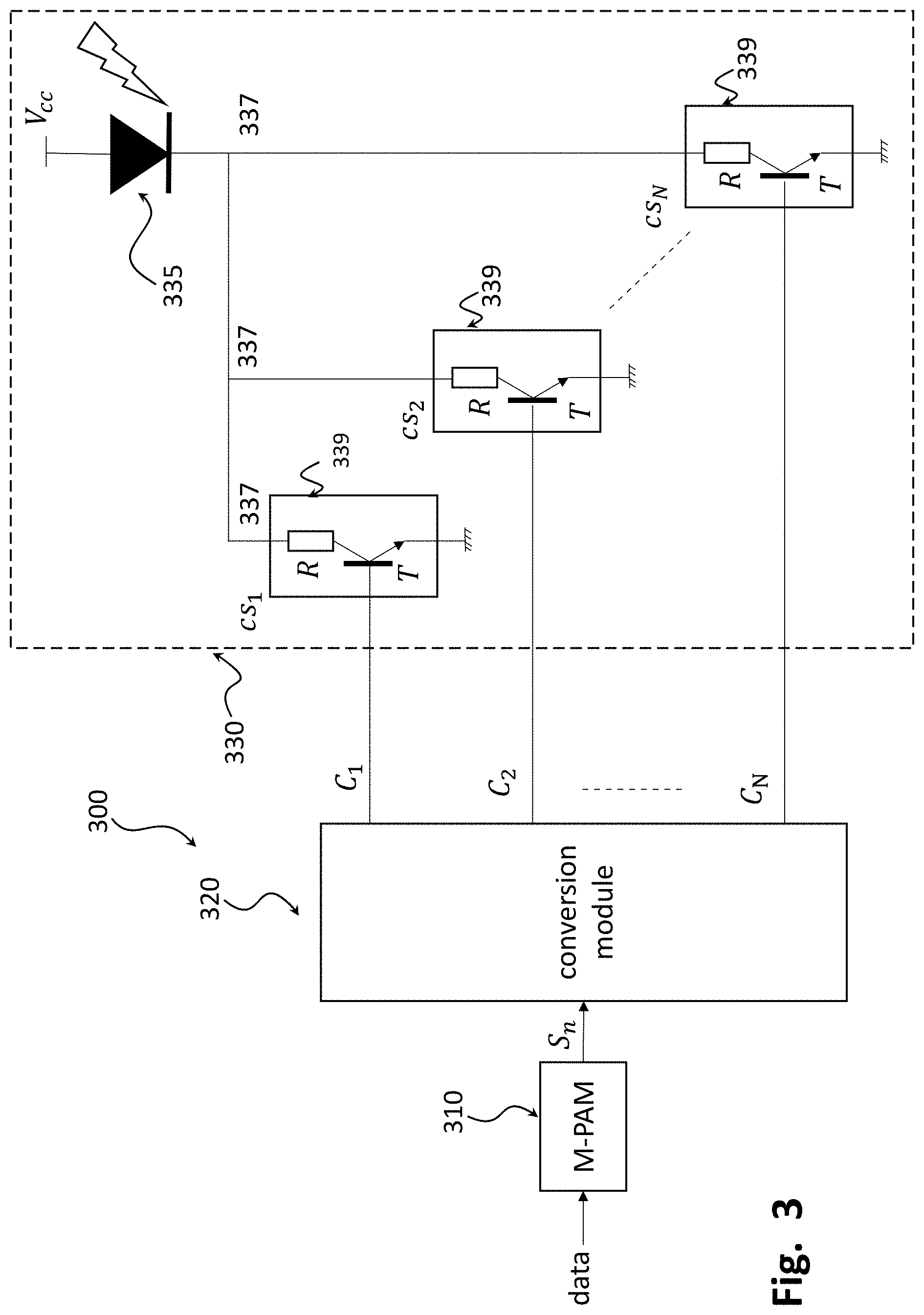
FIG. 3 diagrammatically represents the structure of an emitter with M-PAM modulation for an optical wireless telecommunication system, according to a first embodiment of the invention.
The emitter 300 comprises an M-PAM modulator, 310, modulating the binary data into M-PAM symbols. More precisely, each binary word (with maximum size log.sub.2(M)) is transformed by the modulator into an M-PAM symbol. The M-PAM symbols are then input into a conversion module, 320, that makes a binary word with N bits comprising n bits in a first logical state and N-n bits in a complementary logical state correspond to an M-PAM modulation symbol, S.sub.n, 0.ltoreq.n.ltoreq.N, in which N=M-1 (where M is the size of the PAM alphabet).
The following gives an example of a conversion table for the case M=8 (N=7):
TABLE-US-00001 8-PAM symbol C.sub.1 C.sub.2 C.sub.3 C.sub.4 C.sub.5 C.sub.6 C.sub.7 S.sub.0 0 0 0 0 0 0 0 S.sub.1 1 0 0 0 0 0 0 S.sub.2 1 1 0 0 0 0 0 S.sub.3 1 1 1 0 0 0 0 S.sub.4 1 1 1 1 0 0 0 S.sub.5 1 1 1 1 1 0 0 S.sub.6 1 1 1 1 1 1 0 S.sub.7 1 1 1 1 1 1 1
The 8-PAM symbols at the input are denoted S.sub.0, . . . , S.sub.7 and the output word from the conversion module is denoted C.sub.1, . . . , C.sub.7. It will be noted that the bits in the output word with the first logical value (or the complementary logical value) are not necessarily contiguous in the above example but they can occupy arbitrary positions.
The M-PAM modulator, 310, and the conversion module, 320, are advantageously made using an FPGA programmable circuit or an ASIC type dedicated integrated circuit, or even using a digital signal processor DSP.
According to one particular embodiment, the combination of the M-PAM modulator, 310, and the conversion module, 320, is made using a binary thermometric transcoder, encoding binary words with log.sub.2(M) bits into words with N bits. It will be remembered that the alphabet of a thermometric code on N bits is composed of M mots, each word being composed of 0.ltoreq.n.ltoreq.N LSB bits with a first logical value (for example "1"), the N-n MSB bits having a complementary value. Thus, for example, for M=8, the binary word "101" is encoded "0011111".
Regardless of the envisaged embodiment, each logical output C.sub.1, . . . , C.sub.N of the conversion module controls a switched current source, cs.sub.1, . . . , cs.sub.N, of an optical generator module, 330. This optical generator comprises an optical source, for example a LED, 335 and a plurality N of parallel branches, 337, each of these branches being arranged in series with the optical source between a power supply source V.sub.cc and the ground. Each branch 337 comprises a switched current source, 339, through a logical output of the conversion module 320. For example, each branch comprises a transistor T operating in saturated-blocked mode, mounted in series with a resistor R. The transistor may be a bipolar transistor or a MOS transistor. The characteristics of transistors (T) and values of resistors (R) are chosen to be identical in each branch. Thus, all current sources generate an identical current I.sub.0 and the emission current from the optical source (for example IR LED) can vary from 0 to NI.sub.0 as a function of the data to be emitted. However, if the characteristics of transistors in the different branches are not precisely the same, a resistor calibration phase can advantageously be included such that the currents generated by switched current sources are nevertheless identical.
Each switched current source can be made by putting a group of transistors in parallel, if the saturation current of a single transistor is found to be insufficient. In this case, a logical output from the conversion module controls the bases of transistors in said group in parallel.
It will be noted that, unlike prior art, the optical emitter only requires a single light source, the elementary intensities being added in the electrical domain and not in the optical domain.
FIG. 4 diagrammatically represents the structure of an emitter with M-PAM modulation for an optical wireless telecommunication system, according to a second embodiment of the invention.
This embodiment is different from the first embodiment in that the logical outputs from the conversion module are weighted and in that the currents in the different branches are also weighted.
More precisely, the optical emitter comprises an M-PAM modulator, 410, and a conversion module 420. The conversion module, 420, making a binary word with .mu.=log.sub.2(M) bits correspond to each M-PAM modulation symbol, S.sub.n, 0.ltoreq.n.ltoreq.N, in which N=M-1.
As in the first embodiment, the M-PAM modulator, 410, and the conversion module, 420, are advantageously made using an FPGA programmable circuit or an ASIC type dedicated integrated circuit, or even using a digital signal processor DSP.
According to one example, the conversion module can use a particularly simple conversion table in which the modulation level n expressed in binary on .mu.=log.sub.2(M) bits, C.sub.1, . . . , C.sub..mu., is made to correspond to each symbol S.sub.n.
Thus, for the case M=8:
TABLE-US-00002 8-PAM symbol C.sub.1 C.sub.2 C.sub.3 S.sub.0 0 0 0 S.sub.1 1 0 0 S.sub.2 0 1 0 S.sub.3 1 1 0 S.sub.4 0 0 1 S.sub.5 1 0 1 S.sub.6 0 1 1 S.sub.7 1 1 1
In this particularly simple example embodiment, the combination of the M-PAM modulator and the conversion module can be made by a simple series/parallel converter, 3 successive modulator input bits forming an output word from the conversion module. Obviously, other conversion tables are possible by changing over the rows and/or columns of the above table.
Regardless of the envisaged conversion table, each logical output C.sub.1, . . . , C.sub..mu. of the conversion module controls a switched current source, cs.sub.1, . . . , cs.sub..mu., of an optical generator module, 430. Unlike the previous embodiment, the switched current sources have different intensities, the switched current source cs.sub.m, m=1, . . . , .mu. generating a current with intensity 2.sup.m-1I.sub.0 in which I.sub.0 is the current generated by the current source cs.sub.1, associated with the LSB of the output word from the conversion module.
As before, the optical generator 430 comprises an optical source 435 (for example a LED) and a plurality of parallel branches, 437, each of these branches being arranged in series with the optical source between a power supply source V.sub.cc and the ground. However, unlike the first embodiment, the number of branches in this case is equal to .mu.. A branch m comprises a current source 439 designated by cs.sub.m, switched by C.sub.m, and with intensity 2.sup.m-1I.sub.0. The switched current source can be made by a transistor operating in saturated-blocked mode in series with a resistor R.sub.m. Resistance values R.sub.m are determined, possibly during a calibration phase, such that currents generated by cs.sub.1, . . . , cs.sub..mu. are equal to I.sub.0, 2I.sub.0, . . . , 2.sup..mu.-1I.sub.0. Thus, emission current sources from the optical source (for example IR LED) can vary from 0 to NI.sub.0 as a function of the data to be emitted.
Alternatively, according to a variant of the second embodiment, currents from switched current sources are chosen such that the light intensity of the optical source takes on values equal to .PHI..sub.0, 2I.sub.0, . . . , 2.sup..mu.-1.PHI..sub.0 (in which .PHI..sub.0 is a predetermined light power), when current sources cs.sub.1, . . . , cs.sub..mu. respectively are activated, to take account of non-linearities, if any, in the optical source. To achieve this, the resistances are adjusted accordingly in a calibration phase, the resistance R.sub.m, m=0, . . . , .mu.-1 being chosen such that the light intensity of the optical source is equal to 2.sup.m.PHI..sub.0 when the current source cs.sub.m is activated and other current sources are cut off.
It is important to note that the emitter according to the first or the second embodiment can also use a second modulation in addition to the M-PAM modulation. For example, it would be possible for the logical outputs controlling switching of current sources to also be modulated in Pulse Position Modulation (PPM) to provide an additional degree of modulation or in Pulse Width Modulation (PWM) so as to obtain a variation of the degree of lighting.
Furthermore, in the first embodiment and also in the second embodiment, it is possible to not use the control word C.sub.1=C.sub.2= . . . C.sub.N=0 (corresponding to a zero current intensity) to code a PAM symbol, so as to make a distinguish between the symbol in question and a lack of transmission, for example due to a failure.
* * * * *
D00000
D00001
D00002
D00003
D00004
XML
uspto.report is an independent third-party trademark research tool that is not affiliated, endorsed, or sponsored by the United States Patent and Trademark Office (USPTO) or any other governmental organization. The information provided by uspto.report is based on publicly available data at the time of writing and is intended for informational purposes only.
While we strive to provide accurate and up-to-date information, we do not guarantee the accuracy, completeness, reliability, or suitability of the information displayed on this site. The use of this site is at your own risk. Any reliance you place on such information is therefore strictly at your own risk.
All official trademark data, including owner information, should be verified by visiting the official USPTO website at www.uspto.gov. This site is not intended to replace professional legal advice and should not be used as a substitute for consulting with a legal professional who is knowledgeable about trademark law.