Current difference sensors, systems and methods
Ausserlechner , et al. Nov
U.S. patent number 10,488,445 [Application Number 15/603,708] was granted by the patent office on 2019-11-26 for current difference sensors, systems and methods. This patent grant is currently assigned to Infineon Technologies AG. The grantee listed for this patent is Infineon Technologies AG. Invention is credited to Berthold Astegher, Udo Ausserlechner.


| United States Patent | 10,488,445 |
| Ausserlechner , et al. | November 26, 2019 |
Current difference sensors, systems and methods
Abstract
In an embodiment, a current difference sensor includes first and second conductors arranged relative to one another such that when a first current flows through the first conductor and a second current, equal to the first current, flows through the second conductor, a first magnetic field induced in the first conductor and a second magnetic field induced in the second conductor cancel each other at first and second positions; first and second magnetic field sensing elements are arranged at the first and second positions, respectively, and have a first sensitivity to the first and second currents; third and fourth magnetic field sensing elements are arranged at other positions, and have a second sensitivity to the first and second currents; and the first sensitivity is less than the second sensitivity such that the first and second magnetic field sensing elements and not the third and fourth magnetic sensing elements are selected.
| Inventors: | Ausserlechner; Udo (Villach, AT), Astegher; Berthold (Villach, AT) | ||||||||||
|---|---|---|---|---|---|---|---|---|---|---|---|
| Applicant: |
|
||||||||||
| Assignee: | Infineon Technologies AG
(Neubiberg, DE) |
||||||||||
| Family ID: | 46525913 | ||||||||||
| Appl. No.: | 15/603,708 | ||||||||||
| Filed: | May 24, 2017 |
Prior Publication Data
| Document Identifier | Publication Date | |
|---|---|---|
| US 20170285077 A1 | Oct 5, 2017 | |
Related U.S. Patent Documents
| Application Number | Filing Date | Patent Number | Issue Date | ||
|---|---|---|---|---|---|
| 14636573 | Mar 3, 2015 | 9678172 | |||
| 13012096 | Mar 10, 2015 | 8975889 | |||
| Current U.S. Class: | 1/1 |
| Current CPC Class: | G01R 17/02 (20130101); G01R 33/096 (20130101); G01R 15/20 (20130101); G01R 15/202 (20130101); G01R 33/093 (20130101); G01R 15/205 (20130101); G01R 33/06 (20130101) |
| Current International Class: | G01R 17/02 (20060101); G01R 15/20 (20060101); G01R 33/09 (20060101); G01R 33/06 (20060101) |
References Cited [Referenced By]
U.S. Patent Documents
| 3323057 | May 1967 | Haley |
| 4021729 | May 1977 | Hudson, Jr. |
| 4559495 | December 1985 | Lienhard |
| 4894610 | January 1990 | Friedl |
| 5017804 | May 1991 | Harnden et al. |
| 5041780 | August 1991 | Rippel |
| 5173758 | December 1992 | Heremans |
| 5451865 | September 1995 | Coburn |
| 5642041 | June 1997 | Berkcan |
| 5786976 | July 1998 | Field |
| 5963028 | October 1999 | Engel et al. |
| 6040690 | March 2000 | Ladds |
| 6310470 | October 2001 | Hebing et al. |
| 6341416 | January 2002 | Biskeborn et al. |
| 6356068 | March 2002 | Steiner et al. |
| 6424018 | July 2002 | Ohtsuka |
| 6452413 | September 2002 | Burghartz |
| 6462531 | October 2002 | Ohtsuka |
| 6512359 | January 2003 | Tamai et al. |
| 6636029 | October 2003 | Kunze et al. |
| 6683448 | January 2004 | Ohtsuka |
| 6727683 | April 2004 | Goto et al. |
| 6781313 | August 2004 | Aiken |
| 6781358 | August 2004 | Goto |
| 6841989 | January 2005 | Goto et al. |
| 6940265 | September 2005 | Hauenstein et al. |
| 6949927 | September 2005 | Goetz |
| 6995315 | February 2006 | Sharma et al. |
| 7075287 | July 2006 | Mangtani et al. |
| 7129691 | October 2006 | Shibahara et al. |
| 7166807 | January 2007 | Gagnon et al. |
| 7259545 | August 2007 | Stauth et al. |
| 7358724 | April 2008 | Taylor et al. |
| 7375507 | May 2008 | Racz et al. |
| 7474093 | January 2009 | Ausserlechner |
| 7476816 | January 2009 | Doogue et al. |
| 7476953 | January 2009 | Taylor et al. |
| 7492178 | February 2009 | Bidenbach |
| 7525300 | April 2009 | Watanabe et al. |
| 7528593 | May 2009 | Tanizawa |
| 7545136 | June 2009 | Racz et al. |
| 7564239 | July 2009 | Mapps et al. |
| 7605580 | October 2009 | Strzalkowski |
| 7709754 | May 2010 | Doogue et al. |
| 7746056 | June 2010 | Stauth et al. |
| 7816905 | October 2010 | Doogue et al. |
| 7923987 | April 2011 | Ausserlechner |
| 8159254 | April 2012 | Kaltalioglu |
| 8217643 | July 2012 | Kuroki et al. |
| 8283742 | October 2012 | Motz et al. |
| 8421442 | April 2013 | Younsi et al. |
| 8680843 | March 2014 | Ausselechner |
| 8878520 | November 2014 | Tamura |
| 8963536 | February 2015 | Ausselechner |
| 8975889 | March 2015 | Ausselechner et al. |
| 9222992 | December 2015 | Ausselechner et al. |
| 2001/0052780 | December 2001 | Hayat-Dawoodi |
| 2003/0155905 | August 2003 | Hauenstein |
| 2004/0155644 | August 2004 | Stauth et al. |
| 2005/0030004 | February 2005 | Takatsuka et al. |
| 2005/0270013 | December 2005 | Berkcan et al. |
| 2005/0270014 | December 2005 | Zribi et al. |
| 2006/0076947 | April 2006 | Berkcan et al. |
| 2006/0082983 | April 2006 | Parkhill |
| 2006/0103381 | May 2006 | Schmollngruber |
| 2006/0255797 | November 2006 | Taylor et al. |
| 2006/0284613 | December 2006 | Hastings et al. |
| 2007/0063690 | March 2007 | De Wilde et al. |
| 2007/0170533 | July 2007 | Doogue |
| 2007/0290682 | December 2007 | Oohira |
| 2008/0035923 | February 2008 | Tschmelitsch et al. |
| 2008/0143329 | June 2008 | Ishihara |
| 2008/0297138 | December 2008 | Taylor et al. |
| 2008/0312854 | December 2008 | Chemin et al. |
| 2008/0316655 | December 2008 | Shoji |
| 2009/0021249 | January 2009 | Kumar et al. |
| 2009/0026560 | January 2009 | Wombacher et al. |
| 2009/0050990 | February 2009 | Aono et al. |
| 2009/0058412 | March 2009 | Taylor et al. |
| 2009/0128130 | May 2009 | Stauth et al. |
| 2009/0152595 | June 2009 | Kaga et al. |
| 2009/0184704 | July 2009 | Guo et al. |
| 2009/0294882 | December 2009 | Sterling |
| 2009/0295368 | December 2009 | Doogue et al. |
| 2009/0322325 | December 2009 | Ausserlechner |
| 2010/0045285 | February 2010 | Ohmori et al. |
| 2010/0045286 | February 2010 | Hotz et al. |
| 2010/0117638 | May 2010 | Yamashita et al. |
| 2010/0156394 | June 2010 | Ausserlechner et al. |
| 2010/0182002 | July 2010 | Van Zon et al. |
| 2010/0231198 | September 2010 | Bose et al. |
| 2010/0237853 | September 2010 | Bose et al. |
| 2010/0315095 | December 2010 | Younsi et al. |
| 2011/0062956 | March 2011 | Edelstein |
| 2011/0204887 | March 2011 | Ausserlechner et al. |
| 2011/0133732 | June 2011 | Sauber |
| 2011/0172938 | July 2011 | Gu et al. |
| 2011/0221429 | September 2011 | Tamura |
| 2011/0227560 | September 2011 | Haratani et al. |
| 2011/0234215 | September 2011 | Ausserlechner |
| 2011/0248711 | October 2011 | Ausserlechner |
| 2011/0298454 | December 2011 | Ausserlechner |
| 2011/0304327 | December 2011 | Ausserlechner |
| 2012/0049884 | March 2012 | Kaitalioglu |
| 2012/0086433 | April 2012 | Cheng et al. |
| 2012/0112365 | May 2012 | Ausseriechner et al. |
| 2012/0146164 | June 2012 | Ausserlechner |
| 2012/0146165 | June 2012 | Ausserlechner et al. |
| 2012/0262152 | October 2012 | Ausserlechner |
| 2013/0106412 | May 2013 | Nomura et al. |
| 2013/0265041 | October 2013 | Friedrich et al. |
| 1095162 | Nov 1994 | CN | |||
| 1132858 | Oct 1996 | CN | |||
| 1261959 | Aug 2000 | CN | |||
| 1885044 | Dec 2006 | CN | |||
| 101495874 | Jul 2009 | CN | |||
| 201514439 | Jun 2010 | CN | |||
| 19821492 | Nov 1999 | DE | |||
| 29819486 | Mar 2000 | DE | |||
| 19946935 | May 2001 | DE | |||
| 10051160 | May 2002 | DE | |||
| 10233129 | Feb 2003 | DE | |||
| 10231194 | Feb 2004 | DE | |||
| 602005003777 12 | Dec 2008 | DE | |||
| 202010011725 | Jan 2011 | DE | |||
| 2002243766 | Aug 2002 | JP | |||
| 2006208278 | Aug 2006 | JP | |||
| 0123899 | Apr 2001 | WO | |||
| 2005033718 | Apr 2005 | WO | |||
| 2009119238 | Oct 2006 | WO | |||
| 2008008140 | Jan 2008 | WO | |||
| 2009088767 | Jul 2009 | WO | |||
| 2010048037 | Apr 2010 | WO | |||
Other References
|
Steiner, et al. "Fully Packaged CMOS Current Monitor Using Lead-On-Chip Technology." Physical Electronics Laboratory, pp. 603-608. .COPYRGT. 1998. cited by applicant . Lutz, et al. "Double-Sided Low-Temperature Joining Technique for Power Cycling Capability at High Temperature," EPE 2005-Dresden, ISBN 90-75815-08-5. cited by applicant . Schwarzbauer, et al. "Novel Large Area Joining Technique for Improved Power Device Performance." IEEE Transactions on Industry Applications, vol. 27, No. 1, pp. 93-95, 1991. cited by applicant . Allegro, Allegro Hall Effect-Based Current Sensor ICs: Revolutionary, high accuracy, high bandwidth current sensing!, www.allegomicro.com/en/Products/Design/curren_sensors/index.asp, 5 Pages. .COPYRGT. 2010. cited by applicant . Allegro, Hall-Effect Sensor IC's: Current Sensor ICs, 1 Page, .COPYRGT. 2010. cited by applicant . Allegro, High Bandwidth, Fast Fault Response Current Sensor IC in Thermally Enhanced Package. ACS709-DS, www.microallegro.com, 16 pages, .COPYRGT. 2008-2009. cited by applicant . Allegro, Fully Integrated Hall Effect-Based Linear Current Sensor IC with 2.1 KvRMS Isolation and a Low-Resistance Current Conductor, ACS712-DS, Rev. 13, 14 pages, .COPYRGT. 2006-2010. cited by applicant . Sandireddy, Sandhya, IEEE Xplore, .COPYRGT. 2005, Advanced Wafer ThinningTechnologies to Enable Multichip Packages, pp. 24-27. cited by applicant . Hopkins, Allegro Microsystems, Inc., High Performance Power Ics and Hall Effect Sensor, "Hall Effect Technology for Server, Backplane and Power Supply Applications." IBM 2008 Power and Cooling Symposium, Sep. 30, 2008, 34 pages. cited by applicant . Chinese Application No. 201210018577.6, Filed Jan. 20, 2012, Chinese First Office Action, dated Jan. 3, 2014. cited by applicant . Yang, Lixin, Differential Current Transducer for Localization Type A Metro Vehicle, Journal of Railway, Engineering Society, Issue 10, Oct. 31, 2007, pp. 89-92. cited by applicant . Non-Final Office Action dated May 30, 2013 for U.S. Appl. No. 12/711,471. cited by applicant . Notice of Allowance dated Dec. 20, 2013 for U.S. Appl. No. 12/711,471. cited by applicant . Notice of Allowance dated Feb. 9, 2017 for U.S. Appl. No. 14/636,573. cited by applicant . Final Office Action dated Oct. 28, 2016 for U.S. Appl. No. 14/636,573. cited by applicant . Non-Final Office Action dated Dec. 14, 2015 for U.S. Appl. No. 14/636,573. cited by applicant . Notice of Allowance dated Oct. 31, 2014 for U.S. Appl. No. 13/012,096. cited by applicant . Final Office Action dated Aug. 5, 2014 for U.S. Appl. No. 13/012,096. cited by applicant . Non-Final Office Action dated Jan. 28, 2014 for U.S. Appl. No. 13/012,096. cited by applicant . Non-Final Office Action dated Sep. 16, 2013 for U.S. Appl. No. 13/012,096. cited by applicant. |
Primary Examiner: Patidar; Jay
Attorney, Agent or Firm: Eschweiler & Potashnik, LLC
Parent Case Text
REFERENCE TO RELATED APPLICATION
This application is a Divisional application of U.S. application Ser. No. 14/636,573 filed on Mar. 3, 2015, which is a Continuation of U.S. application Ser. No. 13/012,096 filed on Jan. 24, 2011, the contents of which are incorporated by reference in their entirety.
Claims
The invention claimed is:
1. A current sensor comprising: a plurality of conductors comprising a first conductor configured to conduct a first current that generates a first magnetic field in a first direction, and a second conductor configured to conduct a second current that generates a second magnetic field in the first direction, wherein the first conductor is separate from the second conductor, wherein the plurality of conductors are configured to generate the first and second magnetic fields with a magnitude and a direction such that the first magnetic field in the first direction and the second magnetic field in the first direction are each approximately canceled at a first location and a second location; and a plurality of magnetic field sensing elements arranged at a plurality of locations, respectively, on a face of a die, wherein first and second magnetic field sensing elements of the plurality of magnetic field sensing elements are configured to act as a first pair of sensing elements to sense a superposition of the first magnetic field and the second magnetic field in the first direction at the first and second locations, respectively, and third and fourth magnetic field sensing elements of the plurality of magnetic field sensing elements are configured to act as a second pair of sensing elements to sense the superposition of the first magnetic field and the second magnetic field in the first direction at third and fourth locations, respectively; wherein the first pair of sensing elements has a first sensitivity to a sum of the first current and the second current, and the second pair of sensing elements has a second sensitivity to the sum of the first current and the second current, the first sensitivity being lower than the second sensitivity; and wherein the first pair of sensing elements and not the second pair of sensing elements is selected to provide information regarding at least one of a difference or a sum of the first current and the second current, based on the first magnetic field and the second magnetic field.
2. The current sensor of claim 1, wherein the first current and the second current are approximately equal.
3. The current sensor of claim 1, wherein the first conductor is wider than the second conductor.
4. The current sensor of claim 1, wherein the first conductor and the second conductor of the plurality of conductors form a U-shaped conductor element respectively with a connecting portion therebetween.
5. The current sensor of claim 1, wherein the first magnetic field sensing element is arranged approximately at the first location and is configured to sense the first magnetic field and the second magnetic field in the first direction, wherein the second magnetic field sensing element is arranged at the second location and is configured to sense the first magnetic field and the second magnetic field in the first direction, and wherein the plurality of magnetic field sensing elements further comprise: a first orthogonal magnetic field sensor element arranged opposite of the first magnetic field sensing element and forming a first half-bridge with the first magnetic field sensing element; and a second orthogonal magnetic field sensor element arranged opposite of the second magnetic field sensing element and forming a second half-bridge with the second magnetic field sensing element.
6. The current sensor of claim 5, wherein the first half-bridge and the second half-bridge are in close proximity to one another such that they are configured to generate temperature compensated signals, respectively.
7. The current sensor of claim 1, wherein at least two conductors of the plurality of conductors are laterally asymmetrical with respect to one another.
Description
TECHNICAL FIELD
The invention relates generally to current sensors and more particularly to current difference sensors suitable, for example, for sensing small current differences.
BACKGROUND
Conventional current difference sensing systems often use a ring-shaped ferrite. Two wires are coupled to the ring such that two currents flow through the ring in opposite directions and their flux contributions cancel. If the two currents are different, a net flux is carried by the ferrite, which can be detected by a secondary winding and processed electronically.
While such systems can be effective for detecting current differences, they provide only limited information. For example, they can detect whether |I1-I2|>threshold but do not provide any reliable information regarding I1+I2 or I1-I2.
Therefore, there is a need for improved current difference sensing systems and methods.
SUMMARY
Current difference sensors, systems and methods are disclosed. In an embodiment, a current difference sensor comprises first and second conductors arranged relative to one another such that when a first current flows through the first conductor and a second current, equal to the first current, flows through the second conductor, a first magnetic field caused by the first current and a second magnetic field caused by the second current cancel each other at a first position and a second position; and first and second magnetic field sensing elements arranged to detect the first and second magnetic fields.
In an embodiment, a method comprises inducing a first current to flow in a first conductor; inducing a second current to flow in a second conductor; arranging the first and second conductors such that at least one component of a total magnetic field caused by the first and second currents is approximately zero in at least two locations when the first and second currents are approximately equal; positioning magnetic field sensors in the at least two locations; and determining a difference between the first and second currents based on sensed magnetic fields.
In an embodiment, a method comprises arranging a first conductor spaced apart from and substantially parallel to a second conductor; arranging a die proximate the first and second conductors; and arranging a plurality of magnetic field sensing elements on a first surface of the die to detect magnetic fields caused by first and second currents in the first and second conductors, respectively, and determine a difference between the first and second currents based on the magnetic fields.
BRIEF DESCRIPTION OF THE DRAWINGS
The invention may be more completely understood in consideration of the following detailed description of various embodiments of the invention in connection with the accompanying drawings, in which:
FIG. 1 depicts a side cross-sectional view of a current difference sensor according to an embodiment.
FIG. 2 depicts a side cross-sectional view of a current difference sensor according to an embodiment.
FIG. 3 depicts a side cross-sectional view of a current difference sensor according to an embodiment.
FIG. 4 depicts a graph of magnetic fields for various die and conductor arrangements according to an embodiment.
FIG. 5 depicts a side cross-sectional view of a current difference sensor according to an embodiment.
FIG. 6 depicts a side cross-sectional view of a current difference sensor according to an embodiment.
FIG. 7 depicts a side cross-sectional view of a current difference sensor according to an embodiment.
FIG. 8 depicts a side cross-sectional view of a current difference sensor according to an embodiment.
FIG. 9 depicts orthogonal magnetic field sensor elements according to an embodiment.
FIG. 10A depicts a side cross-sectional view of a current difference sensor according to an embodiment.
FIG. 10B depicts a top plan view of the current difference sensor of FIG. 10A.
FIG. 11 depicts a side cross-sectional view of a current difference sensor according to an embodiment.
FIG. 12 depicts a side cross-sectional view of a current difference sensor according to an embodiment.
FIG. 13 depicts a top plan view of a current difference sensor according to an embodiment.
FIG. 14A depicts a top plan view of a current difference sensor conductor according to an embodiment.
FIG. 14B depicts a top plan view of a current difference sensor conductor according to an embodiment.
FIG. 14C depicts a top plan view of the current difference sensor conductors of FIGS. 14A and 14B.
FIG. 14D is a side cross-sectional view of the current difference sensor of FIGS. 14A-14C.
While the invention is amenable to various modifications and alternative forms, specifics thereof have been shown by way of example in the drawings and will be described in detail. It should be understood, however, that the intention is not to limit the invention to the particular embodiments described. On the contrary, the intention is to cover all modifications, equivalents, and alternatives falling within the spirit and scope of the invention as defined by the appended claims.
DETAILED DESCRIPTION
Embodiments relate to current difference sensors. In various embodiments, a current difference sensor can compare two currents and detect a difference therebetween. In one embodiment, the detectable difference can be as small as about 10 mA for currents in a range of about zero to about 30 A, though this can vary in other embodiments. Additionally, embodiments can provide reduced delay times, such as below about 1 microsecond, and provide information regarding I1+I2 as well as I1-I2. Further, embodiments are small in size, robust against interference and inexpensive.
Embodiments comprise two conductors arranged such that when equal currents pass therethrough, magnetic field contributions of each conductor cancel at points at which magnetic field sensor elements, sensing the same magnetic field components, can be arranged. Unequal, or difference, currents can then be detected, with the components subtracted in order to cancel homogeneous background fields.
Referring to FIG. 1, an embodiment of a current difference sensor 100 is depicted. Sensor 100 comprises two conductors 102 and 104 spaced apart from one another on two different planes or levels. A die 106 is arranged therebetween on a third plane or level, and two magnetoresistors (MRs) 108 and 110 are disposed on die 106. MRs 108 and 110 are spaced apart from one another and disposed on a plane approximately midway between conductors 102 and 104 and therefore between currents I1 and I2 in conductors 102 and 104, respectively. In embodiments, MRs 108 and 110 can comprise anisotropic MRs, giant MRs or some other MR effect technology.
Because of assembly tolerances and other factors, however, it is virtually impossible in practice to position MRs 108 and 110 exactly midway between conductors 102 and 104. The resulting magnetic fields, Bx1 on MR 108 and Bx2 on MR 110, therefore are as follows: Bx1=(K+dK)*I1-(K-dK)*I2 Bx2=(K'+dK')*I1-(K'-dK')*I2 Bx1-Bx2=(K-K')*(I1-I2)+(dK-dK')*(I1+I2) The difference measurement, Bx1-Bx2, is thus corrupted by the sum of the currents, I1+I2. One solution to this issue would be to provide several MRs on the top surface of die 106 and then select the MRs which have the best suppression of (I1+I2). Because this is generally not a good solution, another solution is to add Hall plates to sensor 100, with a first, H1, arranged proximate MR 108 and a second, H2, arranged proximate MR 110. Then: H2-H1=Kz*(I1+I2) which leads to: I1-I2=[(Bx1-Bx2)/(K-K')]-[(dK-dK')*(H2-H1)/(Kz*(K-K'))] An advantage of this configuration is that it has a low resistance because conductors 102 and 104, in an embodiment, are simple straight bars. Additionally, information regarding I1+I2 and I1-I2 can be obtained.
Another embodiment is depicted in FIG. 2, in which die 106 is mounted in a slightly tilted orientation with respect to the planes of conductors 102 and 104. The tilt angle of die 106 can vary but is generally configured to be larger than worst-case assembly tolerances. Additionally, a plurality of MRs 108 and 110 are arranged on the top surface of die 106. While only MRs 108 and 110 are visible in FIG. 2, this embodiment of sensor 100 comprises additional MRs arranged in a grid on the top surface of die 106, spaced apart by, for example, 25 micrometers along the x-axis. The spacing can vary in other embodiments. After assembly of sensor 100, the signals of all MRs 108 and 110 as well as the grid are tested, and those having the lowest sensitivity to I1+I2 are selected.
Another embodiment is depicted in FIG. 3, in which a small, generally arbitrary lateral asymmetry is introduced between conductors 102 and 104. As in the embodiment of FIG. 2, a grid of MRs 108 and 110 and others not visible in FIG. 3 is arranged on the top surface of die 106, and those having the lowest sensitivity to I1+I2 are selected. In an embodiment, conductors 102 and 104 are each about 6 mm by about 1 mm and are shifted relative to each other by less than about 1 mm in the x-direction in embodiments, such as by about 0.2 mm in one embodiment.
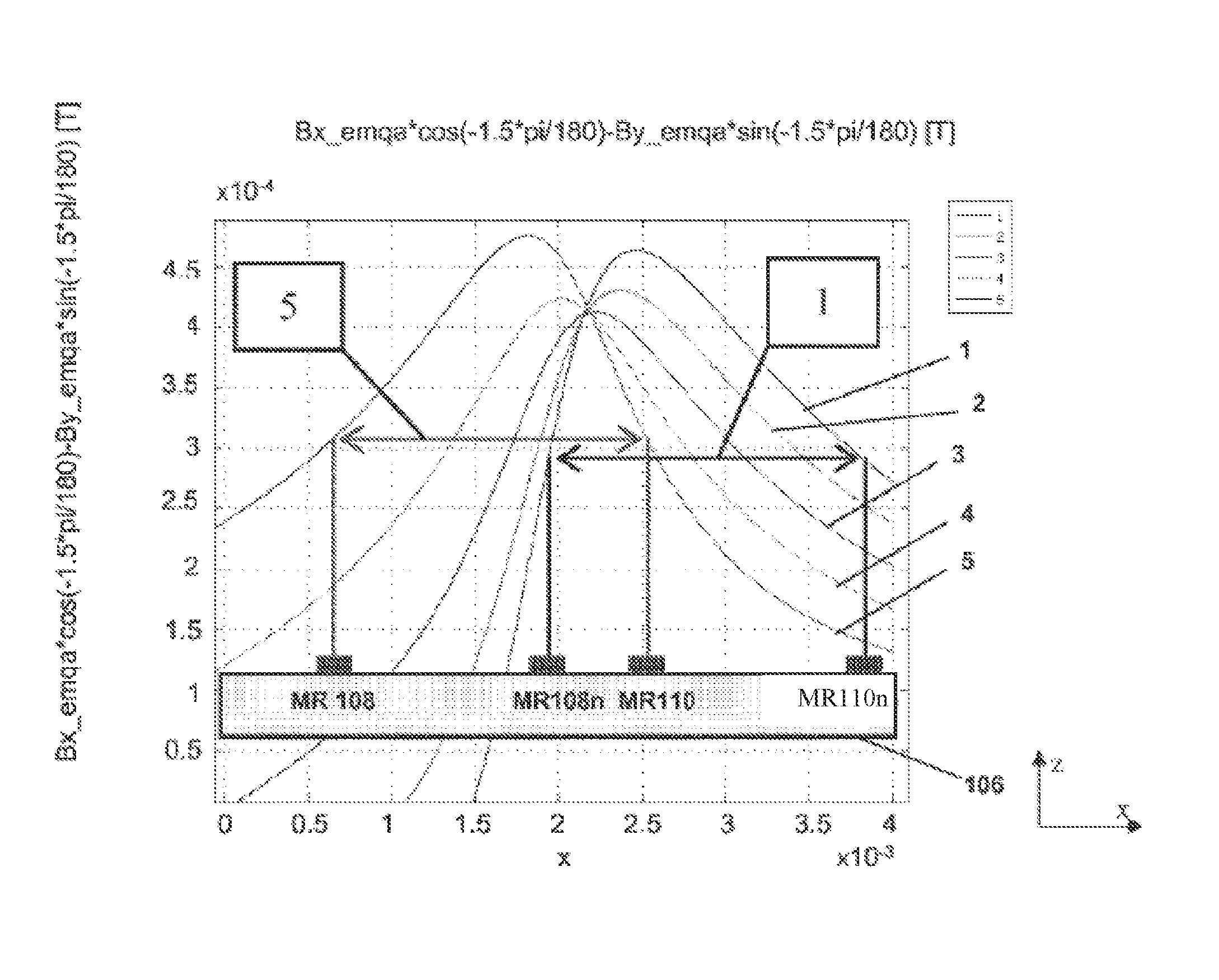
Because of assembly tolerances, it is assumed, for purposes of this example embodiment, that die 106 is tilted by about 1.5 degrees around the symmetry center of conductors 102 and 104. Referring also to FIG. 4, the magnetic field Bx for five different scenarios is depicted, for all of which I1=I2=30 A and z=0.5 mm. For scenario 1, die 106 is shifted 100 .mu.m (from center) toward conductor 104. For scenario 2, die 106 is shifted 50 .mu.m (from center) toward conductor 104. For scenario 3, die 106 is at center. For scenario 4, die 106 is shifted 50 .mu.m toward conductor 102. For scenario 5, die 106 is shifted 100 .mu.m toward conductor 102.
In back-end test, after die 106 is mounted between conductors 102 and 104, the voltage difference of MRs 108-108n and 110-110n arranged in a grid on the top surface of die 106 as previously mentioned can be measured. Note that the grids of MR 108-108n and MR 110-110n may or may not overlap in embodiments. As depicted in FIG. 4, the respective grids do not overlap. The two MRs having the lowest sensitivity with respect to (I1+I2) can be selected. FIG. 4 shows five curves 1-5 corresponding to five different scenarios 1-5, where each curve represents the magnetic field parallel to the die surface versus x-position. For scenario 1, FIG. 4 shows that the field on MR 108n is equal to the field on MR 110n, so that the difference is zero. Thus, in end-of-line testing, sensor 100 could be trimmed by selecting MR 108n and MR 110n. For scenario 5 in FIG. 4, the field on MR 108 is the same as the one on MR 110. Therefore, these two MRs can be selected during the trimming process. This makes it possible in embodiments to trim sensor 100 such that it does not respond to (I1+I2) but rather only (I1-I2). Any mismatch of the MRs is also trimmed by this procedure.
Referring again to FIG. 3, the concept can be generalized. Conductors 102 and 104 are of similar shape and carry the same current such that midway between the two, the respective magnetic fields of conductors 102 and 104 cancel to a large extent, in the sense that the magnitude of the total field is much less, e.g. by a factor of 100 or 1,000, than the magnitude of the fields caused by a single conductor. Conductors 102 and 104 are formed to have a small asymmetry such that the lateral magnetic field caused by identical currents in both conductors 102 and 104 exhibits a small peak at a certain position x for all assembly tolerances between conductors 102 and 104 and die 106. For all tolerances, there is at least one MR (108 or 110) to the left and one MR (110 or 108) to the right of the peak, with the lateral magnetic field identical on both MRs 108 and 110.
The asymmetry depicted in FIG. 3 is obtained by shifting conductor 104 slightly laterally with respect to conductor 102. In another embodiment, conductor 104 could be made slightly wider than conductor 102 such that the right edges of each are positioned as in FIG. 4 with the left edges flush. In yet another embodiment, the cross-sectional area of one of the conductors 102 or 104 can be tapered such that it is thicker (in the vertical direction with respect to the orientation of the drawing on the page) at the left side than the right, or vice-versa. Or, both conductors 102 and 104 can be tapered yet positioned such that the thicker end of one is flush with the thinner end of the other.
Other embodiments are also possible. In the embodiment of FIG. 5, sensor 100 comprises first and second conductors 102 and 104 mounted to a bottom side of a printed circuit board (PCB) 114 to isolate the conductors 102 and 104 from die 106, which is mounted to a top side of PCB 114. In embodiments, PCB 114 can be replaced by some other non-conducting structure comprising, for example, glass, porcelain or some other suitable material. Three MRs 108, 110 and 112 are mounted to a top side of die 106. In an embodiment, MRs 108 and 110 are separated by 1.25 mm, and MRs 110 and 112 are separated by 1.25 mm, such that MRs 108 and 112 are separated by 2.5 mm, though these dimensions can vary in embodiments. With currents in conductors 102 and 104 flowing into the drawing plane as depicted in FIG. 5, MR 108 detects a strong field from the current through conductor 102 and weak field from the current through conductor 104, whereas MR 112 responds more strongly to current through conductor 104 than through conductor 102. MR 110 responds equally to the currents in conductors 102 and 104 such that the field on MR 110 is proportional to the sum of the currents in conductors 102 and 104, whereas the fields on the other MRs 108 and 112 are neither proportional to pure sums nor pure differences of the currents but rather a combination of both.
A challenge with the embodiment of FIG. 5 is balancing sensitivity and saturation. High sensitivity is desired to measure small magnetic fields, but efforts to increase sensitivity, such as reducing the vertical distance between conductors 102 and 104 and MRs 108, 110 and 112 and/or the cross-sectional dimensions of conductors 102 and 104, can send the MRs into saturation such that larger current differences can no longer be detected. Such an embodiment can be suitable for various desired applications, however.
Another embodiment is depicted in FIG. 6, in which sensor 100 comprises three conductors 102, 103 and 104. Center conductor 103 can be used to "tune" sensor 100 such that positions are obtained without a magnetic field, and MRs 108 and 110 can then be arranged accordingly to see no net field. In an embodiment, conductors 102 and 104 are each about 1.2 mm by about 1.2 mm, and conductor 103 is about 1.7 mm by about 1.7 mm. Die 106 is coupled to a wafer 116, which is about 200 .mu.m thick and comprises glass or porcelain or some other suitable material in embodiments and includes through-vias 120. Vias 120 are filled with a conductor, such as a nano-paste, in embodiments. In one embodiment, the silicon of die 106 is ground down to about 30 .mu.m and adhesively bonded at its top side to wafer 116. Die(s) 106 can then be cut or otherwise formed into rectangles, and the bottom side(s) and sidewalls coated with a low-temperature dioxide or silicon oxide (SiOx). In an embodiment, the dioxide is about 15 .mu.m thick. MRs 108 and 110 are spaced apart about x=2 mm and are separated from the top side of conductors 102-104 by about z=50 .mu.m in an embodiment. Conductors 102-104, die 106 and wafer 116 are covered by a mold compound 118.
In an embodiment, current flows into the drawing plane (as depicted in FIG. 6) through center conductor 103 and out of the drawing plane (again, as depicted in FIG. 6) through outer conductors 102 and 104, each of which carries about half of the current. MR sensors 108 and 110 form a bridge and are arranged at locations where the magnetic fields of conductor 103 and either of conductors 102 and 104 cancel at equal currents.
A further adaptation of sensor 100 of FIG. 6 is depicted in FIG. 7, in which sensor 100 comprises a dual-die package. One MR 108 is coupled to an upper die 106a, and another MR 110 is coupled to a lower die 106b, with MRs 108 and 110 located on a common axis in an embodiment. Conductors 102 and 104 are similar to conductor 103 in an embodiment and are about 1.7 mm by about 1.7 mm. Such an embodiment can provide advantages with respect to obtaining information about (I1+I2) and improve cancellation of background of fields. In an embodiment of sensor 100 of FIG. 7, wafers 116 can be omitted.
It can be difficult, because of assembly tolerances and other factors, to arrange MRs 108 and 110 on the same axis, represented by a dashed vertical line in FIG. 7. Therefore, another, potentially more robust embodiment of sensor 100 depicted in FIG. 8 can address this challenge by including additional MRs 109 and 111. In an embodiment, conductors 102 and 104 are each about 0.9 mm by about 1.7 mm, and conductor 103 is about 1.7 mm by about 1.7 mm. Conductors 102-104 are cast into glass 122 in an embodiment, and contacts 124 couple PCBs 114a and 114b. MRs 108-111 are separated from conductors 102-104 by z=about 250 .mu.m in embodiments.
In operation, current I1 flows through conductor 103, while current 12 is split into two halves which each flow through one of conductors 102 and 104 in the opposite direction of current I1. The signals of MRs 108 and 109 are added, as are those of MRs 110 and 111, with the latter then subtracted from the former. Because MRs 108 and 110 experience strong I1 fields, while MRs 109 and 111 experience strong I2 fields of the opposite polarity of I1, lateral positioning shifts of the MRs 108-111 are compensated for. Casting conductors 102-104 in glass helps to avoid dimensional changes over the lifetime thereof due to moisture and other factors.
A potential drawback of the embodiment of FIG. 8, however, is the expense of a dual-die solution. In various embodiments, temperature can also be an issue. To provide temperature compensation, orthogonal MRs can be added, an embodiment of which is depicted in FIG. 9. FIG. 9 depicts two MRs 108 and 110, each with an orthogonal MR 108' and 110' forming half-bridges. Embodiments comprising additional MRs, such as grids of MRs as discussed herein, can similarly comprise additional orthogonal MRs. In operation, and with the barber poles as depicted in FIG. 9, MRs 108 and 110 are sensitive to weak fields in the x-direction, while MRs 108' and 110' are sensitive to weak fields in the -x-direction. The close arrangements of MRs 108 and 108', and 110 and 110', ensures that each sees the same magnetic field and temperature. The signals of each half-bridge, U1 and U2, are therefore temperature compensated.
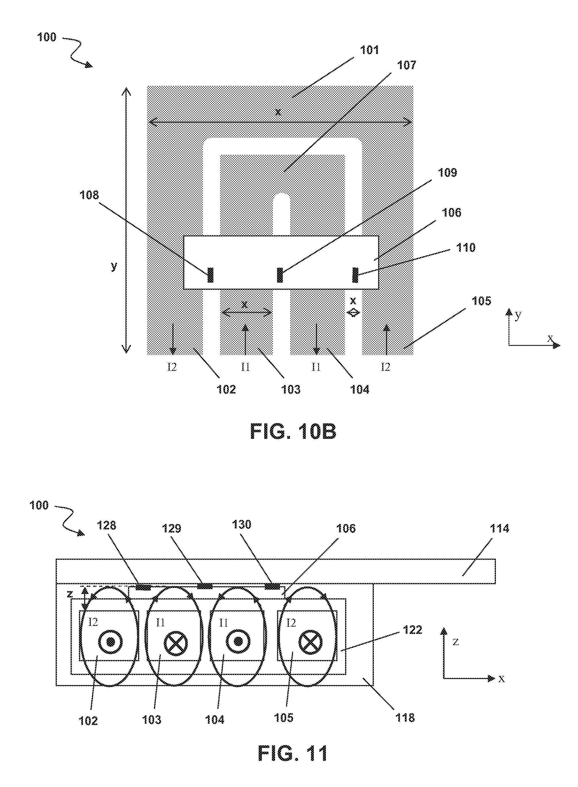
Another embodiment of a sensor 100 is depicted in FIG. 10. In this embodiment, sensor 100 comprises a single die 106, with three MRs 108, 109 and 100 mounted on a top surface thereof. Although the dimensions can vary in embodiments, in one embodiment die 106 can be about 4 mm by about 1.75 mm, with a thickness of about 200 .mu..mu.m, and MRs 108 and 110 are spaced apart by x=about 4 mm. Four conductors 102, 103, 104 and 105 are cast into glass 122, similar to the embodiment of FIG. 8, with a top surface of conductors 102-105 spaced apart from MRs 108-110 by z=about 250 .mu.m in an embodiment. As depicted in FIG. 10B, conductors 102-105 comprise conductor portions, with conductors 102 and 105, along with a connecting portion 101, forming a first generally U-shaped conductor element, and conductors 103 and 104, along with a connecting portion 107, forming a second generally U-shaped conductor element. A cross-section of each of conductors 102-105 as depicted in FIG. 10A is about 1.7 mm by about 1.7 mm in an embodiment. In FIG. 10B, the length of conductors 102 and 105 is y=about 10 mm, with a width of x=about 8.3 mm of connecting portion 101. A separation distance between adjacent ones of the conductors 102-15 is x=about 0.5 mm in the embodiment depicted.
Advantages of the embodiment of FIG. 10 include a single die, which is less expensive and provides easier assembly, because it does not require pins for communication with a second die. A single die also provides fewer opportunities for mismatch of the MR sensor elements as well as improved temperature homogeneity. The MRs of FIG. 10 can comprise orthogonal MRs, such as are depicted in FIG. 9 and discussed above, in embodiments.
Sensor system 100 depicted in FIG. 11 is similar to that of FIG. 10 but comprises a triple Hall element 128, 129 and 130 system in addition to MRs to measure the sum of the currents I1+I2. Advantages of the embodiment of FIG. 11 include increased robustness against disturbances and improved tamper-resistance.
On the other hand, Hall elements 128-130 should be positioned closer to conductors 102-105. Therefore, another embodiment (not depicted) comprises Hall elements 128-130 on a bottom side of die 106 and MRs on a top side of die 106. Die 106 can be about 200 .mu.m thick in such an embodiment.
Alternatively, AMRs 108 and 110 can be implemented to measure I1+x*I2 (x<<1), as depicted in the embodiment of FIG. 12. AMRs 108 and 100 can be positioned on a top surface of die 106, which can be about 200 .mu.m thick in an embodiment, such that a separation distance between AMRs 108 and 110 and top surfaces of conductors 102-15 is z=about 250 .mu.m. Such a system is generally robust against background fields, though not as robust as the triple Hall embodiment of FIG. 11. The small damping effect, x, is due to the distance between conductors 102 and 105, through which current I2 flows, and AMRs 108 and 110.
In the embodiment of FIG. 13, a return path for I2 is omitted, such that only three conductors 102-104 are implemented. The conductors 102-104, however, can be made wider, such as x=about 3.5 mm for each of conductors 103 and 104 and x=about 6 mm for conductor 102, and dissipation reduced by about 50%. A separation distance between conductors 103 and 104 is still x=about 0.5 mm in an embodiment, and a length of conductor 102 is y=about 10 mm in an embodiment.
Yet another embodiment is depicted in FIG. 14, in which sensor system 100 comprises a multi-level conductor 132, at least somewhat similar to the embodiments discussed above with respect to FIGS. 1-4. Conductor 132 (FIG. 14C) comprises a first layer 134 (FIG. 14A) and a second layer 136 (FIG. 14B) in an embodiment. In an embodiment, isolation layers 138 are positioned between die 106 and conductor level 136, and between conductor level 136 and conductor level 134.
Various embodiments of current and current difference sensing and determination systems are disclosed. Embodiments can be advantageous by providing single sensor systems capable of measuring current flow (I1+I2) and leakage currents (I1-I2) while also being small in size, robust against interference and inexpensive when compared with conventional difference current sensor systems. Embodiments can also be combined with an isolated voltage sensor in order to obtain a full power measurement.
Various embodiments of systems, devices and methods have been described herein. These embodiments are given only by way of example and are not intended to limit the scope of the invention. It should be appreciated, moreover, that the various features of the embodiments that have been described may be combined in various ways to produce numerous additional embodiments. Moreover, while various materials, dimensions, shapes, configurations and locations, etc. have been described for use with disclosed embodiments, others besides those disclosed may be utilized without exceeding the scope of the invention.
Persons of ordinary skill in the relevant arts will recognize that the invention may comprise fewer features than illustrated in any individual embodiment described above. The embodiments described herein are not meant to be an exhaustive presentation of the ways in which the various features of the invention may be combined. Accordingly, the embodiments are not mutually exclusive combinations of features; rather, the invention may comprise a combination of different individual features selected from different individual embodiments, as understood by persons of ordinary skill in the art.
Any incorporation by reference of documents above is limited such that no subject matter is incorporated that is contrary to the explicit disclosure herein. Any incorporation by reference of documents above is further limited such that no claims included in the documents are incorporated by reference herein. Any incorporation by reference of documents above is yet further limited such that any definitions provided in the documents are not incorporated by reference herein unless expressly included herein.
For purposes of interpreting the claims for the present invention, it is expressly intended that the provisions of Section 112, sixth paragraph of 35 U.S.C. are not to be invoked unless the specific terms "means for" or "step for" are recited in a claim.
* * * * *
References
D00000
D00001
D00002
D00003
D00004
D00005
D00006
D00007
D00008
XML
uspto.report is an independent third-party trademark research tool that is not affiliated, endorsed, or sponsored by the United States Patent and Trademark Office (USPTO) or any other governmental organization. The information provided by uspto.report is based on publicly available data at the time of writing and is intended for informational purposes only.
While we strive to provide accurate and up-to-date information, we do not guarantee the accuracy, completeness, reliability, or suitability of the information displayed on this site. The use of this site is at your own risk. Any reliance you place on such information is therefore strictly at your own risk.
All official trademark data, including owner information, should be verified by visiting the official USPTO website at www.uspto.gov. This site is not intended to replace professional legal advice and should not be used as a substitute for consulting with a legal professional who is knowledgeable about trademark law.