Organic electroluminescent materials and devices
Hung , et al. Oc
U.S. patent number 10,461,260 [Application Number 14/294,336] was granted by the patent office on 2019-10-29 for organic electroluminescent materials and devices. This patent grant is currently assigned to Universal Display Corporation. The grantee listed for this patent is Universal Display Corporation. Invention is credited to Yi-Tza Hung, Raymond Kwong, Ken-Tsung Wong, Chuanjun Xia.


View All Diagrams
| United States Patent | 10,461,260 |
| Hung , et al. | October 29, 2019 |
Organic electroluminescent materials and devices
Abstract
A luminescent materials including donor-acceptor compounds with a nitrogen containing donor connected to the 1-position of a carbazole and triazene acceptor connected at the 9-position is disclosed.
| Inventors: | Hung; Yi-Tza (Taipei, TW), Wong; Ken-Tsung (Taipei, TW), Kwong; Raymond (Shatin, HK), Xia; Chuanjun (Lawrenceville, NJ) | ||||||||||
|---|---|---|---|---|---|---|---|---|---|---|---|
| Applicant: |
|
||||||||||
| Assignee: | Universal Display Corporation
(Ewing, NJ) |
||||||||||
| Family ID: | 54702811 | ||||||||||
| Appl. No.: | 14/294,336 | ||||||||||
| Filed: | June 3, 2014 |
Prior Publication Data
| Document Identifier | Publication Date | |
|---|---|---|
| US 20150349273 A1 | Dec 3, 2015 | |
| Current U.S. Class: | 1/1 |
| Current CPC Class: | H01L 51/0072 (20130101); C07D 403/10 (20130101); H01L 51/0061 (20130101); C09K 11/06 (20130101); C07D 409/14 (20130101); C07D 487/06 (20130101); C07D 403/04 (20130101); C07D 403/14 (20130101); H01L 51/0067 (20130101); C07D 405/14 (20130101); C07D 401/14 (20130101); H01L 51/5012 (20130101); H01L 51/5036 (20130101); H01L 2251/308 (20130101); H01L 51/0074 (20130101); H01L 51/5016 (20130101); H01L 2251/5376 (20130101); H01L 51/0073 (20130101) |
| Current International Class: | H01L 51/00 (20060101); C07D 409/14 (20060101); C07D 487/06 (20060101); C07D 401/14 (20060101); C07D 403/14 (20060101); C09K 11/06 (20060101); C07D 405/14 (20060101); C07D 403/10 (20060101); C07D 403/04 (20060101); H01L 51/50 (20060101) |
| Field of Search: | ;257/258 |
References Cited [Referenced By]
U.S. Patent Documents
| 4769292 | September 1988 | Tang et al. |
| 5061569 | October 1991 | VanSlyke et al. |
| 5247190 | September 1993 | Friend et al. |
| 5703436 | December 1997 | Forrest et al. |
| 5707745 | January 1998 | Forrest et al. |
| 5834893 | November 1998 | Bulovic et al. |
| 5844363 | December 1998 | Gu et al. |
| 6013982 | January 2000 | Thompson et al. |
| 6087196 | July 2000 | Sturm et al. |
| 6091195 | July 2000 | Forrest et al. |
| 6097147 | August 2000 | Baldo et al. |
| 6294398 | September 2001 | Kim et al. |
| 6303238 | October 2001 | Thompson et al. |
| 6337102 | January 2002 | Forrest et al. |
| 6468819 | October 2002 | Kim et al. |
| 6528187 | March 2003 | Okada |
| 6687266 | February 2004 | Ma et al. |
| 6835469 | December 2004 | Kwong et al. |
| 6921915 | July 2005 | Takiguchi et al. |
| 7087321 | August 2006 | Kwong et al. |
| 7090928 | August 2006 | Thompson et al. |
| 7154114 | December 2006 | Brooks et al. |
| 7250226 | July 2007 | Tokito et al. |
| 7279704 | October 2007 | Walters et al. |
| 7332232 | February 2008 | Ma et al. |
| 7338722 | March 2008 | Thompson et al. |
| 7393599 | July 2008 | Thompson et al. |
| 7396598 | July 2008 | Takeuchi et al. |
| 7431968 | October 2008 | Shtein et al. |
| 7445855 | November 2008 | Mackenzie et al. |
| 7534505 | May 2009 | Lin et al. |
| 2002/0034656 | March 2002 | Thompson et al. |
| 2002/0134984 | September 2002 | Igarashi |
| 2002/0158242 | October 2002 | Son et al. |
| 2003/0138657 | July 2003 | Li et al. |
| 2003/0151042 | August 2003 | Marks et al. |
| 2003/0152802 | August 2003 | Tsuboyama et al. |
| 2003/0175553 | September 2003 | Thompson et al. |
| 2003/0230980 | December 2003 | Forrest et al. |
| 2004/0036077 | February 2004 | Ise |
| 2004/0137267 | July 2004 | Igarashi et al. |
| 2004/0137268 | July 2004 | Igarashi et al. |
| 2004/0174116 | September 2004 | Lu et al. |
| 2005/0025993 | February 2005 | Thompson et al. |
| 2005/0112407 | May 2005 | Ogasawara et al. |
| 2005/0238919 | October 2005 | Ogasawara |
| 2005/0244673 | November 2005 | Satoh et al. |
| 2005/0260441 | November 2005 | Thompson et al. |
| 2005/0260449 | November 2005 | Walters et al. |
| 2006/0008670 | January 2006 | Lin et al. |
| 2006/0046098 | March 2006 | Hosokawa |
| 2006/0202194 | September 2006 | Jeong et al. |
| 2006/0240279 | October 2006 | Adamovich et al. |
| 2006/0251923 | November 2006 | Lin et al. |
| 2006/0263635 | November 2006 | Ise |
| 2006/0280965 | December 2006 | Kwong et al. |
| 2007/0190359 | August 2007 | Knowles et al. |
| 2007/0278938 | December 2007 | Yabunouchi et al. |
| 2008/0015355 | January 2008 | Schafer et al. |
| 2008/0018221 | January 2008 | Egen et al. |
| 2008/0106190 | May 2008 | Yabunouchi et al. |
| 2008/0124572 | May 2008 | Mizuki et al. |
| 2008/0220265 | September 2008 | Xia et al. |
| 2008/0297033 | December 2008 | Knowles et al. |
| 2009/0008605 | January 2009 | Kawamura et al. |
| 2009/0009065 | January 2009 | Nishimura et al. |
| 2009/0017330 | January 2009 | Iwakuma et al. |
| 2009/0030202 | January 2009 | Iwakuma et al. |
| 2009/0039776 | February 2009 | Yamada et al. |
| 2009/0045730 | February 2009 | Nishimura et al. |
| 2009/0045731 | February 2009 | Nishimura et al. |
| 2009/0101870 | April 2009 | Pakash et al. |
| 2009/0108737 | April 2009 | Kwong et al. |
| 2009/0115316 | May 2009 | Zheng et al. |
| 2009/0165846 | July 2009 | Johannes et al. |
| 2009/0167162 | July 2009 | Lin et al. |
| 2009/0179554 | July 2009 | Kuma et al. |
| 2010/0099890 | April 2010 | Ogita |
| 2010/0187984 | July 2010 | Lin |
| 2011/0210318 | September 2011 | Bae |
| 2012/0205636 | August 2012 | Kim |
| 2012/0223295 | September 2012 | Inoue |
| 2012/0235136 | September 2012 | Ogawa |
| 2013/0234119 | September 2013 | Mizuki |
| 2013/0264548 | October 2013 | Mizuki et al. |
| 2014/0001446 | January 2014 | Mizuki et al. |
| 2014/0001451 | January 2014 | Mizuki |
| 2014/0084270 | March 2014 | Kato |
| 2014/0145151 | May 2014 | Xia |
| 2014/0151667 | June 2014 | Miyata |
| 2014/0191225 | July 2014 | Inoue et al. |
| 2014/0231794 | August 2014 | Iwakuma et al. |
| 2014/0296519 | October 2014 | Matsumoto |
| 2015/0060801 | March 2015 | Nishimura et al. |
| 2015/0280133 | October 2015 | Parham |
| 2015/0318511 | November 2015 | Kim |
| 2015/0325794 | November 2015 | Nishimura |
| 2016/0197288 | July 2016 | Ikeda |
| 102738413 | Oct 2012 | CN | |||
| 103649268 | Mar 2014 | CN | |||
| 0650955 | May 1995 | EP | |||
| 1725079 | Nov 2006 | EP | |||
| 2034538 | Mar 2009 | EP | |||
| 200511610 | Jan 2005 | JP | |||
| 2007123392 | May 2007 | JP | |||
| 2007254297 | Oct 2007 | JP | |||
| 2008074939 | Apr 2008 | JP | |||
| 2012-216801 | Nov 2012 | JP | |||
| 2013117726 | Oct 2013 | KR | |||
| 2001039234 | May 2001 | WO | |||
| 2002002714 | Jan 2002 | WO | |||
| 200215645 | Feb 2002 | WO | |||
| 2003040257 | May 2003 | WO | |||
| 2003060956 | Jul 2003 | WO | |||
| 2004093207 | Oct 2004 | WO | |||
| 2004107822 | Dec 2004 | WO | |||
| 2005014551 | Feb 2005 | WO | |||
| 2005019373 | Mar 2005 | WO | |||
| 2005030900 | Apr 2005 | WO | |||
| 2005089025 | Sep 2005 | WO | |||
| 2005123873 | Dec 2005 | WO | |||
| 2006009024 | Jan 2006 | WO | |||
| 2006056418 | Jun 2006 | WO | |||
| 2006072002 | Jul 2006 | WO | |||
| 2006082742 | Aug 2006 | WO | |||
| 2006098120 | Sep 2006 | WO | |||
| 2006100298 | Sep 2006 | WO | |||
| 2006103874 | Oct 2006 | WO | |||
| 2006114966 | Nov 2006 | WO | |||
| 2006132173 | Dec 2006 | WO | |||
| 2007002683 | Jan 2007 | WO | |||
| 2007004380 | Jan 2007 | WO | |||
| 2007063754 | Jun 2007 | WO | |||
| 2007063796 | Jun 2007 | WO | |||
| 2008056746 | May 2008 | WO | |||
| 2008101842 | Aug 2008 | WO | |||
| 2008132085 | Nov 2008 | WO | |||
| 2009000673 | Dec 2008 | WO | |||
| 2009003898 | Jan 2009 | WO | |||
| 2009008311 | Jan 2009 | WO | |||
| 2009018009 | Feb 2009 | WO | |||
| 2009050290 | Apr 2009 | WO | |||
| 2009021126 | May 2009 | WO | |||
| 2009062578 | May 2009 | WO | |||
| 2009063833 | May 2009 | WO | |||
| 2009066778 | May 2009 | WO | |||
| 2009066779 | May 2009 | WO | |||
| 2009086028 | Jul 2009 | WO | |||
| 2009100991 | Aug 2009 | WO | |||
| 2011070963 | Jun 2011 | WO | |||
| WO2013012297 | Jan 2013 | WO | |||
| 2013024872 | Feb 2013 | WO | |||
| 2013046635 | Apr 2013 | WO | |||
| 2013129491 | Sep 2013 | WO | |||
| 2013147205 | Oct 2013 | WO | |||
| 2013175747 | Nov 2013 | WO | |||
| 2015076035 | May 2015 | WO | |||
Other References
|
Adachi, Chihaya et al., "Organic Electroluminescent Device Having a Hole Conductor as an Emitting Layer," Appl. Phys. Lett., 55(15): 1489-1491 (1989). cited by applicant . Adachi, Chihaya et al., "Nearly 100% Internal Phosphorescence Efficiency in an Organic Light Emitting Device," J. Appl. Phys., 90(10): 5048-5051 (2001). cited by applicant . Adachi, Chihaya et al., "High-Efficiency Red Electrophosphorescence Devices," Appl. Phys. Lett., 78(11)1622-1624 (2001). cited by applicant . Aonuma, Masaki et al., "Material Design of Hole Transport Materials Capable of Thick-Film Formation in Organic Light Emitting Diodes," Appl. Phys. Lett., 90:183503-1-183503-3. cited by applicant . Baldo et al., Highly Efficient Phosphorescent Emission from Organic Electroluminescent Devices, Nature, vol. 395, 151-154, (1998). cited by applicant . Baldo et al., Very high-efficiency green organic light-emitting devices based on electrophosphorescence, Appl. Phys. Lett., vol. 75, No. 3, 4-6 (1999). cited by applicant . Gao, Zhiqiang et al., "Bright-Blue Electroluminescence From a Silyl-Substituted ter-(phenylene-vinylene) derivative," Appl. Phys. Lett., 74(6): 865-867 (1999). cited by applicant . Guo, Tzung-Fang et al., "Highly Efficient Electrophosphorescent Polymer Light-Emitting Devices," Organic Electronics, 115-20 (2000). cited by applicant . Hamada, Yuji et al., "High Luminance in Organic Electroluminescent Devices with Bis(10-hydroxybenzo[h]quinolinato)beryllium as an Emitter, " Chem. Lett., 905-906 (1993). cited by applicant . Holmes, R.J. et al., "Blue Organic Electrophosphorescence Using Exothermic Host-Guest Energy Transfer," Appl. Phys. Lett., 82(15):2422-2424 (2003). cited by applicant . Hu, Nan-Xing et al., "Novel High Tg Hole-Transport Molecules Based on Indolo[3,2-b]carbazoles for Organic Light-Emitting Devices," Synthetic Metals, 111-112:421-424 (2000). cited by applicant . Huang, Jinsong et al., "Highly Efficient Red-Emission Polymer Phosphorescent Light-Emitting Diodes Based on Two Novel Tris(1-phenylisoquinolinato-C2,N)indium(III) Derivates," Adv. Mater., 19:739-743 (2007). cited by applicant . Huang, Wei-Sheng et al., "Highly Phosphorescent Bis-Cyclometalated Iridium Complexes Containing Benzoimidazole-Based Ligands," Chem. Mater., 16(12):2480-2488 (2004). cited by applicant . Hung, L.S. et al., "Anode Modification in Organic Light-Emitting Diodes by Low-Frequency Plasma Polymerization of CHF3," Appl. Phys. Lett., 78(5):673-675 (2001). cited by applicant . Ikai, Masamichi and Tokito, Shizuo, "Highly Efficient Phosphorescence From Organic Light-Emitting Devices with an Exciton-Block Layer," Appl. Phys. Lett., 79(2):156-158 (2001). cited by applicant . Ikeda, Hisao et al., "P-185 Low-Drive-Voltage OLEDs with a Buffer Layer Having Molybdenum Oxide," SID Symposium Digest, 37:923-926 (2006). cited by applicant . Inada, Hiroshi and Shirota, Yasuhiko, "1,3,5-Tris[4-(diphenylamino)phenyl]benzene and its Methylsubstituted Derivatives as a Novel Class of Amorphous Molecular Materials," J. Mater. Chem., 3(3):319-320 (1993). cited by applicant . Kanno, Hiroshi et al., "Highly Efficient and Stable Red Phosphorescent Organic Light-Emitting Device Using bis[2-(2-benzothiazoyl)phenolato]zinc(II) as host material," Appl. Phys. Lett., 90:123509-1-123509-3 (2007). cited by applicant . Kido, Junji et al., 1,2,4-Triazole Derivative as an Electron Transport Layer in Organic Electroluminescent Devices, Jpn. J. Appl. Phys., 32:L917-L920 (1993). cited by applicant . Kuwabara, Yoshiyuki et al., "Thermally Stable Multilayered Organic Electroluminescent Devices Using Novel Starburst Molecules, 4,4',4''-Tri(N-carbazolyl)triphenylamine (TCTA) and 4,4',4''-Tris(3-methylphenylphenyl-amino) triphenylamine (m-MTDATA), as Hole-Transport Materials," Adv. Mater., 6(9):677-679 (1994). cited by applicant . Kwong, Raymond C. et al., "High Operational Stability of Electrophosphorescent Devices," Appl. Phys. Lett., 81(1) 162-164 (2002). cited by applicant . Lamansky, Sergey et al., "Synthesis and Characterization of Phosphorescent Cyclometalated Iridium Complexes," Inorg. Chem., 40(7):1704-1711 (2001). cited by applicant . Lee, Chang-Lyoul et al., "Polymer Phosphorescent Light-Emitting Devices Doped with Tris(2-phenylpyridine) Iridium as a Triplet Emitter," Appl. Phys. Lett., 77(15)2280-2282 (2000). cited by applicant . Lo, Shih-Chun et al., "Blue Phosphorescence from Indium(III) Complexes at Room Temperature," Chem. Mater., 18(21)5119-5129 (2006). cited by applicant . Ma, Yuguang et al., "Triplet Luminescent Dinuclear-Gold(I) Complex-Based Light-Emitting Diodes with Low Turn-On voltage," Appl. Phys. Lett., 74(10):1361-1363 (1999). cited by applicant . Mi, Bao-Xiu et al., "Thermally Stable Hole-Transporting Material for Organic Light-Emitting Diode an Isoindole Derivative," Chem. Mater., 15(16):3148-3151 (2003). cited by applicant . Nishida, Jun-ichi et al., "Preparation, Characterization, and Electroluminescence Characteristics of .alpha.-Diimine-type Platinum(II) Complexes with Perfluorinated Phenyl Groups as Ligands," Chem. Lett., 34(4): 592-593 (2005). cited by applicant . Niu, Yu-Hua et al., "Highly Efficient Electrophosphorescent Devices with Saturated Red Emission from a Neutral Osmium Complex," Chem. Mater., 17(13):3532-3536 (2005). cited by applicant . Noda, Tetsuya and Shirota,Yasuhiko, "5,5'-Bis(dimesitylboryl)-2,2'-bithiophene and 5,5''-Bis(dimesitylboryl)-2,2'5',2''-terthiophene as a Novel Family of Electron-Transporting Amorphous Molecular Materials," J. Am. Chem. Soc., 120 (37):9714-9715 (1998). cited by applicant . Okumoto, Kenji et al., "Green Fluorescent Organic Light-Emitting Device with External Quantum Efficiency of Nearly 10%," Appl. Phys. Lett., 89:063504-1-063504-3 (2006). cited by applicant . Palilis, Leonidas C., "High Efficiency Molecular Organic Light-Emitting Diodes Based on Silole Derivatives and Their Exciplexes," Organic Electronics, 4:113-121 (2003). cited by applicant . Paulose, Betty Marie Jennifer S. et al., "First Examples of Alkenyl Pyridines as Organic Ligands for Phosphorescent Iridium Complexes," Adv. Mater., 16(22):2003-2007 (2004). cited by applicant . Ranjan, Sudhir et al., "Realizing Green Phosphorescent Light-Emitting Materials from Rhenium(I) Pyrazolato Diimine Complexes," Inorg. Chem., 42(4):1248-1255 (2003). cited by applicant . Sakamoto, Youichi et al., "Synthesis, Characterization, and Electron-Transport Property of Perfluorinated Phenylene Dendrimers," J. Am. Chem. Soc., 122(8):1832-1833 (2000). cited by applicant . Salbeck, J. et al., "Low Molecular Organic Glasses for Blue Electroluminescence," Synthetic Metals, 91209-215 (1997). cited by applicant . Shirota, Yasuhiko et al., "Starburst Molecules Based on p-Electron Systems as Materials for Organic Electroluminescent Devices," Journal of Luminescence, 72-74:985-991 (1997). cited by applicant . Sotoyama, Wataru et al., "Efficient Organic Light-Emitting Diodes with Phosphorescent Platinum Complexes Containing N^C^N-Coordinating Tridentate Ligand," Appl. Phys. Lett., 86:153505-1-153505-3 (2005). cited by applicant . Sun, Yiru and Forrest, Stephen R., "High-Efficiency White Organic Light Emitting Devices with Three Separate Phosphorescent Emission Layers," Appl. Phys. Lett., 91:263503-1-263503-3 (2007). cited by applicant . T. Ostergard et al., "Langmuir-Blodgett Light-Emitting Diodes of Poly(3-Hexylthiophene) Electro-Optical Characteristics Related to Structure," Synthetic Metals, 87:171-177 (1997). cited by applicant . Takizawa, Shin-ya et al., "Phosphorescent Iridium Complexes Based on 2-Phenylimidazo[1,2-.alpha.]pyridine Ligands Tuning of Emission Color toward the Blue Region and Application to Polymer Light-Emitting Devices," Inorg. Chem., 46(10):4308-4319 (2007). cited by applicant . Tang, C.W. and VanSlyke, S.A., "Organic Electroluminescent Diodes," Appl. Phys. Lett., 51(12):913-915 (1987). cited by applicant . Tung, Yung-Liang et al., "Organic Light-Emitting Diodes Based on Charge-Neutral Ru II PHosphorescent Emitters," Adv. Mater., 17(8)1059-1064 (2005). cited by applicant . Van Slyke, S. A. et al., "Organic Electroluminescent Devices with Improved Stability," Appl. Phys. Lett., 69(15):2160-2162 (1996). cited by applicant . Wang, Y. et al., "Highly Efficient Electroluminescent Materials Based on Fluorinated Organometallic Iridium Compounds," Appl. Phys. Lett., 79(4):449-451 (2001). cited by applicant . Wong, Keith Man-Chung et al., A Novel Class of Phosphorescent Gold(III) Alkynyl-Based Organic Light-Emitting Devices with Tunable Colour, Chem. Commun., 2906-2908 (2005). cited by applicant . Wong, Wai-Yeung, "Multifunctional Iridium Complexes Based on Carbazole Modules as Highly Efficient Electrophosphors," Angew. Chem. Int. Ed., 45:7800-7803 (2006). cited by applicant . Goushi, Kenichi et al., "Organic light-emitting diodes employing efficient reverse intersystem crossing for triplet-to singlet state conversion", Nature Photonics, vol. 6, Apr. 2012, pp. 253-258. cited by applicant . Nakagawa, Tetsuya et al., "Electroluminescence based on thermally activated delayed fluorescence generated by a spirobifluorene donor-acceptor structure," Chem. Commun., 2012, 48, pp. 9580-9582. cited by applicant . Mehes, Gabor et al., "Enhanced Electroluminescence Efficiency in a Spiro-Acridine Derivative through Thermally Activated Delayed Fluorescence," Angew. Chem. Int. Ed., 2012, 51, pp. 11311-11315. cited by applicant . Uoyama, Hiroki et al., "Highly efficient organic light-emitting diodes from delayed fluorescence," Nature, Dec. 13, 2012, vol. 492, pp. 234-240. cited by applicant . Endo, Ayataka et al., "Efficient up-conversion of triplet excitons into a singlet state and its application for organic light emitting diodes," Applied Physics Letters, 98, 083302 (2011). cited by applicant . Tanaka, Hiroyuki et al., "Efficient green thermally activated delayed fluorescence (TADF) from phenoxazine-triphenyltriazine (PXZ-TRZ) derivative," Chem. Commun., 2012, 48, pp. 11392-11394. cited by applicant . Zhang, Qisheng et al., "Design of Efficient Thermally Activated Delayed Fluorescence Materials for Pure Blue Organic Light Emitting Diodes," J. Am. Chem. Soc. 2012, 134, pp. 14706-14709. cited by applicant . Notice of Reasons for Rejection dated Jul. 24, 2018 for corresponding Japanese Patent Application No. 2015-105165. cited by applicant. |
Primary Examiner: Everhart; Caridad
Attorney, Agent or Firm: Duane Morris LLP
Claims
What is claimed is:
1. A first device comprising a first organic light emitting device, the first organic light emitting device comprising: an anode; a cathode; and an emissive layer, disposed between the anode and the cathode, wherein the emissive layer comprises a first light emitting compound having a structure according to Formula 1: ##STR00219## wherein R.sup.f is hydrogen and R.sup.a to R.sup.e, R.sup.g, R.sup.1 and R.sup.2 are independently selected from the group consisting of hydrogen, deuterium, halide, alkyl, cycloalkyl, heteroalkyl, arylalkyl, alkoxy, aryloxy, amino, silyl, alkenyl, cycloalkenyl, heteroalkenyl, alkynyl, aryl, heteroaryl, acyl, carbonyl, carboxylic acids, ester, nitrile, isonitrile, sulfanyl, sulfinyl, sulfonyl, phosphino, and combinations thereof; and wherein Ar.sup.1 is ##STR00220## wherein Ar.sup.2 and Ar.sup.3 are independently substituted or unsubstituted aryl or heteroaryl, and Ar.sup.1, Ar.sup.2, and Ar.sup.3 are not connected to one another to form fused ring(s), wherein L is a direct bond or a linker; wherein the first light emitting compound emits a luminescent radiation at room temperature when a voltage is applied across the organic light emitting device; and wherein the luminescent radiation comprises a delayed fluorescence process.
2. The first device of claim 1, wherein the first emitting compound is selected from the group consisting of ##STR00221## ##STR00222## ##STR00223## ##STR00224## ##STR00225## ##STR00226## ##STR00227## ##STR00228## ##STR00229##
3. The first device of claim 1, wherein the emissive layer further comprises a host material.
4. The first device of claim 1, wherein the first device emits a white light at room temperature when a voltage is applied across the organic light emitting device.
5. The first device of claim 1, wherein the emissive layer further comprises a first phosphorescent emitting material.
6. The first device of claim 5, wherein the emissive layer further comprises a second phosphorescent emitting material.
7. A first device comprising a first organic light emitting device, the first organic light emitting device comprising: an anode; a cathode; and an emissive layer, disposed between the anode and the cathode, wherein the emissive layer comprises a first light emitting compound having a structure according to Formula 1: ##STR00230## wherein R.sup.f is hydrogen and R.sup.a to R.sup.e, R.sup.g, R.sup.1 and R.sup.2 are independently selected from the group consisting of hydrogen, deuterium, halide, alkyl, cycloalkyl, heteroalkyl, arylalkyl, alkoxy, aryloxy, amino, silyl, alkenyl, cycloalkenyl, heteroalkenyl, alkynyl, aryl, heteroaryl, acyl, carbonyl, carboxylic acids, ester, nitrile, isonitrile, sulfanyl, sulfinyl, sulfonyl, phosphino, and combinations thereof; and wherein Ar.sup.1 is ##STR00231## wherein Ar.sup.2 and Ar.sup.3 are independently substituted or unsubstituted aryl or heteroaryl, and and Ar.sup.1, Ar.sup.2, and Ar.sup.3 are not connected to one another to form fused ring(s), wherein L is a direct bond or a linker; and wherein the emissive layer further comprises a first phosphorescent emitting material.
8. The first device of claim 7, wherein the emissive layer further comprises a second phosphorescent emitting material.
9. The first device of claim 7, wherein the first device emits a white light at room temperature when a voltage is applied across the organic light emitting device.
10. The first device of claim 7, wherein the emissive layer further comprises a host material.
11. The first device of claim 7, wherein the first emitting compound is selected from the group consisting of ##STR00232## ##STR00233## ##STR00234## ##STR00235## ##STR00236## ##STR00237## ##STR00238## ##STR00239## ##STR00240## ##STR00241##
12. A consumer product comprising an organic light-emitting device comprising: an anode; a cathode; and an emissive layer, disposed between the anode and the cathode, wherein the emissive layer comprises a first light emitting compound having a structure according to Formula 1: ##STR00242## wherein R.sup.f is hydrogen and R.sup.a to R.sup.e, R.sup.g, R.sup.1 and R.sup.2 are independently selected from the group consisting of hydrogen, deuterium, halide, alkyl, cycloalkyl, heteroalkyl, arylalkyl, alkoxy, aryloxy, amino, silyl, alkenyl, cycloalkenyl, heteroalkenyl, alkynyl, aryl, heteroaryl, acyl, carbonyl, carboxylic acids, ester, nitrile, isonitrile, sulfanyl, sulfinyl, sulfonyl, phosphino, and combinations thereof; and wherein Ar.sup.1 is ##STR00243## wherein Ar.sup.2 and Ar.sup.3 are independently substituted or unsubstituted aryl or heteroaryl, and Ar.sup.1, Ar.sup.2, and Ar.sup.3 are not connected to one another to form fused ring(s), wherein L is a direct bond or a linker; and wherein at least one of the following is true: (i) the first light emitting compound emits a luminescent radiation at room temperature when a voltage is applied across the organic light emitting device, and the luminescent radiation comprises a delayed fluorescence process; or (ii) the emissive layer further comprises a first phosphorescent emitting material.
13. The consumer product of claim 12, wherein the consumer product is one of a flat panel display, a computer monitor, a medical monitor, a television, a billboard, a light for interior or exterior illumination and/or signaling, a heads-up display, a fully transparent display, a flexible display, a laser printer, a telephone, a mobile phone, a personal digital assistant (PDA), a laptop computer, a digital camera, a camcorder, a viewfinder, a micro-display, a 3-D display, a vehicle, a large area wall, theater or stadium screen, and a sign.
14. The consumer product of claim 12, wherein the first light emitting compound emits a luminescent radiation at room temperature when a voltage is applied across the organic light emitting device, and the luminescent radiation comprises a delayed fluorescence process.
15. The consumer product of claim 12, wherein the emissive layer further comprises a first phosphorescent emitting material.
Description
PARTIES TO A JOINT RESEARCH AGREEMENT
The claimed invention was made by, on behalf of, and/or in connection with one or more of the following parties to a joint university corporation research agreement: Regents of the University of Michigan, Princeton University, University of Southern California, and the Universal Display Corporation. The agreement was in effect on and before the date the claimed invention was made, and the claimed invention was made as a result of activities undertaken within the scope of the agreement.
FIELD OF THE INVENTION
The present invention relates to organic light emitting devices. More specifically, the present disclosure pertains to luminescent materials comprising donor-acceptor compounds with a nitrogen containing donor connected to the 1-position of a carbazole and triazene as the acceptor for use as emitters in organic light emitting diodes.
BACKGROUND
Opto-electronic devices that make use of organic materials are becoming increasingly desirable for a number of reasons. Many of the materials used to make such devices are relatively inexpensive, so organic opto-electronic devices have the potential for cost advantages over inorganic devices. In addition, the inherent properties of organic materials, such as their flexibility, may make them well suited for particular applications such as fabrication on a flexible substrate. Examples of organic opto-electronic devices include organic light emitting devices (OLEDs), organic phototransistors, organic photovoltaic cells, and organic photodetectors. For OLEDs, the organic materials may have performance advantages over conventional materials. For example, the wavelength at which an organic emissive layer emits light may generally be readily tuned with appropriate dopants.
OLEDs make use of thin organic films that emit light when voltage is applied across the device. OLEDs are becoming an increasingly interesting technology for use in applications such as flat panel displays, illumination, and backlighting. Several OLED materials and configurations are described in U.S. Pat. Nos. 5,844,363, 6,303,238, and 5,707,745, which are incorporated herein by reference in their entirety.
One application for phosphorescent emissive molecules is a full color display. Industry standards for such a display call for pixels adapted to emit particular colors, referred to as "saturated" colors. In particular, these standards call for saturated red, green, and blue pixels. Color may be measured using CIE coordinates, which are well known to the art.
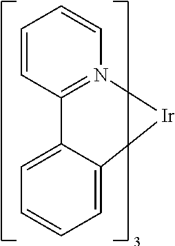
One example of a green emissive molecule is tris(2-phenylpyridine) iridium, denoted Ir(ppy).sub.3, which has the following structure:
##STR00001##
In this, and later figures herein, we depict the dative bond from nitrogen to metal (here, Ir) as a straight line.
As used herein, the term "organic" includes polymeric materials as well as small molecule organic materials that may be used to fabricate organic opto-electronic devices. "Small molecule" refers to any organic material that is not a polymer, and "small molecules" may actually be quite large. Small molecules may include repeat units in some circumstances. For example, using a long chain alkyl group as a substituent does not remove a molecule from the "small molecule" class. Small molecules may also be incorporated into polymers, for example as a pendent group on a polymer backbone or as a part of the backbone. Small molecules may also serve as the core moiety of a dendrimer, which consists of a series of chemical shells built on the core moiety. The core moiety of a dendrimer may be a fluorescent or phosphorescent small molecule emitter. A dendrimer may be a "small molecule," and it is believed that all dendrimers currently used in the field of OLEDs are small molecules.
As used herein, "top" means furthest away from the substrate, while "bottom" means closest to the substrate. Where a first layer is described as "disposed over" a second layer, the first layer is disposed further away from substrate. There may be other layers between the first and second layer, unless it is specified that the first layer is "in contact with" the second layer. For example, a cathode may be described as "disposed over" an anode, even though there are various organic layers in between.
As used herein, "solution processible" means capable of being dissolved, dispersed, or transported in and/or deposited from a liquid medium, either in solution or suspension form.
A ligand may be referred to as "photoactive" when it is believed that the ligand directly contributes to the photoactive properties of an emissive material. A ligand may be referred to as "ancillary" when it is believed that the ligand does not contribute to the photoactive properties of an emissive material, although an ancillary ligand may alter the properties of a photoactive ligand.
As used herein, and as would be generally understood by one skilled in the art, a first "Highest Occupied Molecular Orbital" (HOMO) or "Lowest Unoccupied Molecular Orbital" (LUMO) energy level is "greater than" or "higher than" a second HOMO or LUMO energy level if the first energy level is closer to the vacuum energy level. Since ionization potentials (IP) are measured as a negative energy relative to a vacuum level, a higher HOMO energy level corresponds to an IP having a smaller absolute value (an IP that is less negative). Similarly, a higher LUMO energy level corresponds to an electron affinity (EA) having a smaller absolute value (an EA that is less negative). On a conventional energy level diagram, with the vacuum level at the top, the LUMO energy level of a material is higher than the HOMO energy level of the same material. A "higher" HOMO or LUMO energy level appears closer to the top of such a diagram than a "lower" HOMO or LUMO energy level.
As used herein, and as would be generally understood by one skilled in the art, a first work function is "greater than" or "higher than" a second work function if the first work function has a higher absolute value. Because work functions are generally measured as negative numbers relative to vacuum level, this means that a "higher" work function is more negative. On a conventional energy level diagram, with the vacuum level at the top, a "higher" work function is illustrated as further away from the vacuum level in the downward direction. Thus, the definitions of HOMO and LUMO energy levels follow a different convention than work functions.
More details on OLEDs, and the definitions described above, can be found in U.S. Pat. No. 7,279,704, which is incorporated herein by reference in its entirety.
SUMMARY OF THE INVENTION
According to an embodiment of the present disclosure, a compound having a structure according to the following Formula 1 is disclosed:
##STR00002## In Formula 1, R.sup.a to R.sup.g, R.sup.1 and R.sup.2 are independently selected from the group consisting of hydrogen, deuterium, halide, alkyl, cycloalkyl, heteroalkyl, arylalkyl, alkoxy, aryloxy, amino, silyl, alkenyl, cycloalkenyl, heteroalkenyl, alkynyl, aryl, heteroaryl, acyl, carbonyl, carboxylic acids, ester, nitrile, isonitrile, sulfanyl, sulfinyl, sulfonyl, phosphino, and combinations thereof. Ar.sup.1 to Ar.sup.3 are independently substituted or unsubstituted aryl or heteroaryl and can connect to one another to form fused ring(s). L is a direct bond or a linker.
According to another embodiment, a first device comprising a first organic light emitting device is disclosed. The first organic light emitting device comprising: an anode; a cathode; and an emissive layer, disposed between the anode and the cathode, wherein the emissive layer comprises a first emitting compound having a structure according to Formula 1:
##STR00003## In Formula 1, R.sup.a to R.sup.g, R.sup.1 and R.sup.2 are independently selected from the group consisting of hydrogen, deuterium, halide, alkyl, cycloalkyl, heteroalkyl, arylalkyl, alkoxy, aryloxy, amino, silyl, alkenyl, cycloalkenyl, heteroalkenyl, alkynyl, aryl, heteroaryl, acyl, carbonyl, carboxylic acids, ester, nitrile, isonitrile, sulfanyl, sulfinyl, sulfonyl, phosphino, and combinations thereof. Ar.sup.1 to Ar.sup.3 are independently substituted or unsubstituted aryl or heteroaryl and can connect to one another to form fused ring(s). L is a direct bond or a linker.
According to yet another embodiment, a formulation comprising a compound having a structure according to Formula 1 is also disclosed.
The compound of the present disclosure can be used in OLEDs as emitters, hosts, charge transport materials, in both single color or multiple color devices. The compound can be easily utilized in fabrication of OLEDs because the compound can be vapor-evaporated or solution processed. The compound is useful as emitters because it provides high efficiency OLEDs without using organometallic compounds.
BRIEF DESCRIPTION OF THE DRAWINGS
FIG. 1 shows an organic light emitting device that can incorporate the inventive host material disclosed herein.
FIG. 2 shows an inverted organic light emitting device that can incorporate the inventive host material disclosed herein.
FIG. 3 shows Formula 1 as disclosed herein.
DETAILED DESCRIPTION
Generally, an OLED comprises at least one organic layer disposed between and electrically connected to an anode and a cathode. When a current is applied, the anode injects holes and the cathode injects electrons into the organic layer(s). The injected holes and electrons each migrate toward the oppositely charged electrode. When an electron and hole localize on the same molecule, an "exciton," which is a localized electron-hole pair having an excited energy state, is formed. Light is emitted when the exciton relaxes via a photoemissive mechanism. In some cases, the exciton may be localized on an excimer or an exciplex. Non-radiative mechanisms, such as thermal relaxation, may also occur, but are generally considered undesirable.
The initial OLEDs used emissive molecules that emitted light from their singlet states ("fluorescence") as disclosed, for example, in U.S. Pat. No. 4,769,292, which is incorporated by reference in its entirety. Fluorescent emission generally occurs in a time frame of less than 10 nanoseconds.
More recently, OLEDs having emissive materials that emit light from triplet states ("phosphorescence") have been demonstrated. Baldo et al., "Highly Efficient Phosphorescent Emission from Organic Electroluminescent Devices," Nature, vol. 395, 151-154, 1998; ("Baldo-1") and Baldo et al., "Very high-efficiency green organic light-emitting devices based on electrophosphorescence," Appl. Phys. Lett., vol. 75, No. 3, 4-6 (1999) ("Baldo-II"), which are incorporated by reference in their entireties. Phosphorescence is described in more detail in U.S. Pat. No. 7,279,704 at cols. 5-6, which are incorporated by reference.
FIG. 1 shows an organic light emitting device 100. The figures are not necessarily drawn to scale. Device 100 may include a substrate 110, an anode 115, a hole injection layer 120, a hole transport layer 125, an electron blocking layer 130, an emissive layer 135, a hole blocking layer 140, an electron transport layer 145, an electron injection layer 150, a protective layer 155, a cathode 160, and a barrier layer 170. Cathode 160 is a compound cathode having a first conductive layer 162 and a second conductive layer 164. Device 100 may be fabricated by depositing the layers described, in order. The properties and functions of these various layers, as well as example materials, are described in more detail in U.S. Pat. No. 7,279,704 at cols. 6-10, which are incorporated by reference.
More examples for each of these layers are available. For example, a flexible and transparent substrate-anode combination is disclosed in U.S. Pat. No. 5,844,363, which is incorporated by reference in its entirety. An example of a p-doped hole transport layer is m-MTDATA doped with F.sub.4-TCNQ at a molar ratio of 50:1, as disclosed in U.S. Patent Application Publication No. 2003/0230980, which is incorporated by reference in its entirety. Examples of host materials are disclosed in U.S. Pat. No. 6,303,238 to Thompson et al., which is incorporated by reference in its entirety. An example of an n-doped electron transport layer is BPhen doped with Li at a molar ratio of 1:1, as disclosed in U.S. Patent Application Publication No. 2003/0230980, which is incorporated by reference in its entirety. U.S. Pat. Nos. 5,703,436 and 5,707,745, which are incorporated by reference in their entireties, disclose examples of cathodes including compound cathodes having a thin layer of metal such as Mg:Ag with an overlying transparent, electrically-conductive, sputter-deposited ITO layer. The theory and use of blocking layers is described in more detail in U.S. Pat. No. 6,097,147 and U.S. Patent Application Publication No. 2003/0230980, which are incorporated by reference in their entireties. Examples of injection layers are provided in U.S. Patent Application Publication No. 2004/0174116, which is incorporated by reference in its entirety. A description of protective layers may be found in U.S. Patent Application Publication No. 2004/0174116, which is incorporated by reference in its entirety.
FIG. 2 shows an inverted OLED 200. The device includes a substrate 210, a cathode 215, an emissive layer 220, a hole transport layer 225, and an anode 230. Device 200 may be fabricated by depositing the layers described, in order. Because the most common OLED configuration has a cathode disposed over the anode, and device 200 has cathode 215 disposed under anode 230, device 200 may be referred to as an "inverted" OLED. Materials similar to those described with respect to device 100 may be used in the corresponding layers of device 200. FIG. 2 provides one example of how some layers may be omitted from the structure of device 100.
The simple layered structure illustrated in FIGS. 1 and 2 is provided by way of non-limiting example, and it is understood that embodiments of the invention may be used in connection with a wide variety of other structures. The specific materials and structures described are exemplary in nature, and other materials and structures may be used. Functional OLEDs may be achieved by combining the various layers described in different ways, or layers may be omitted entirely, based on design, performance, and cost factors. Other layers not specifically described may also be included. Materials other than those specifically described may be used. Although many of the examples provided herein describe various layers as comprising a single material, it is understood that combinations of materials, such as a mixture of host and dopant, or more generally a mixture, may be used. Also, the layers may have various sublayers. The names given to the various layers herein are not intended to be strictly limiting. For example, in device 200, hole transport layer 225 transports holes and injects holes into emissive layer 220, and may be described as a hole transport layer or a hole injection layer. In one embodiment, an OLED may be described as having an "organic layer" disposed between a cathode and an anode. This organic layer may comprise a single layer, or may further comprise multiple layers of different organic materials as described, for example, with respect to FIGS. 1 and 2.
Structures and materials not specifically described may also be used, such as OLEDs comprised of polymeric materials (PLEDs) such as disclosed in U.S. Pat. No. 5,247,190 to Friend et al., which is incorporated by reference in its entirety. By way of further example, OLEDs having a single organic layer may be used. OLEDs may be stacked, for example as described in U.S. Pat. No. 5,707,745 to Forrest et al., which is incorporated by reference in its entirety. The OLED structure may deviate from the simple layered structure illustrated in FIGS. 1 and 2. For example, the substrate may include an angled reflective surface to improve outcoupling, such as a mesa structure as described in U.S. Pat. No. 6,091,195 to Forrest et al., and/or a pit structure as described in U.S. Pat. No. 5,834,893 to Bulovic et al., which are incorporated by reference in their entireties.
Unless otherwise specified, any of the layers of the various embodiments may be deposited by any suitable method. For the organic layers, preferred methods include thermal evaporation, ink-jet, such as described in U.S. Pat. Nos. 6,013,982 and 6,087,196, which are incorporated by reference in their entireties, organic vapor phase deposition (OVPD), such as described in U.S. Pat. No. 6,337,102 to Forrest et al., which is incorporated by reference in its entirety, and deposition by organic vapor jet printing (OVJP), such as described in U.S. Pat. No. 7,431,968, which is incorporated by reference in its entirety. Other suitable deposition methods include spin coating and other solution based processes. Solution based processes are preferably carried out in nitrogen or an inert atmosphere. For the other layers, preferred methods include thermal evaporation. Preferred patterning methods include deposition through a mask, cold welding such as described in U.S. Pat. Nos. 6,294,398 and 6,468,819, which are incorporated by reference in their entireties, and patterning associated with some of the deposition methods such as ink-jet and OVJD. Other methods may also be used. The materials to be deposited may be modified to make them compatible with a particular deposition method. For example, substituents such as alkyl and aryl groups, branched or unbranched, and preferably containing at least 3 carbons, may be used in small molecules to enhance their ability to undergo solution processing. Substituents having 20 carbons or more may be used, and 3-20 carbons is a preferred range. Materials with asymmetric structures may have better solution processibility than those having symmetric structures, because asymmetric materials may have a lower tendency to recrystallize. Dendrimer substituents may be used to enhance the ability of small molecules to undergo solution processing.
Devices fabricated in accordance with embodiments of the present invention may further optionally comprise a barrier layer. One purpose of the barrier layer is to protect the electrodes and organic layers from damaging exposure to harmful species in the environment including moisture, vapor and/or gases, etc. The barrier layer may be deposited over, under or next to a substrate, an electrode, or over any other parts of a device including an edge. The barrier layer may comprise a single layer, or multiple layers. The barrier layer may be formed by various known chemical vapor deposition techniques and may include compositions having a single phase as well as compositions having multiple phases. Any suitable material or combination of materials may be used for the barrier layer. The barrier layer may incorporate an inorganic or an organic compound or both. The preferred barrier layer comprises a mixture of a polymeric material and a non-polymeric material as described in U.S. Pat. No. 7,968,146, PCT Pat. Application Nos. PCT/US2007/023098 and PCT/US2009/042829, which are herein incorporated by reference in their entireties. To be considered a "mixture", the aforesaid polymeric and non-polymeric materials comprising the barrier layer should be deposited under the same reaction conditions and/or at the same time. The weight ratio of polymeric to non-polymeric material may be in the range of 95:5 to 5:95. The polymeric material and the non-polymeric material may be created from the same precursor material. In one example, the mixture of a polymeric material and a non-polymeric material consists essentially of polymeric silicon and inorganic silicon.
Devices fabricated in accordance with embodiments of the invention may be incorporated into a wide variety of consumer products, including flat panel displays, computer monitors, medical monitors, televisions, billboards, lights for interior or exterior illumination and/or signaling, heads up displays, fully transparent displays, flexible displays, laser printers, telephones, cell phones, personal digital assistants (PDAs), laptop computers, digital cameras, camcorders, viewfinders, micro-displays, 3-D displays, vehicles, a large area wall, theater or stadium screen, or a sign. Various control mechanisms may be used to control devices fabricated in accordance with the present invention, including passive matrix and active matrix. Many of the devices are intended for use in a temperature range comfortable to humans, such as 18 degrees C. to 30 degrees C., and more preferably at room temperature (20-25 degrees C.), but could be used outside this temperature range, for example, from -40 degree C. to +80 degree C.
The materials and structures described herein may have applications in devices other than OLEDs. For example, other optoelectronic devices such as organic solar cells and organic photodetectors may employ the materials and structures. More generally, organic devices, such as organic transistors, may employ the materials and structures.
The term "halo" or "halogen" as used herein includes fluorine, chlorine, bromine, and iodine.
The term "alkyl" as used herein contemplates both straight and branched chain alkyl radicals. Preferred alkyl groups are those containing from one to fifteen carbon atoms and includes methyl, ethyl, propyl, isopropyl, butyl, isobutyl, tert-butyl, and the like. Additionally, the alkyl group may be optionally substituted.
The term "cycloalkyl" as used herein contemplates cyclic alkyl radicals. Preferred cycloalkyl groups are those containing 3 to 7 carbon atoms and includes cyclopropyl, cyclopentyl, cyclohexyl, and the like. Additionally, the cycloalkyl group may be optionally substituted.
The term "alkenyl" as used herein contemplates both straight and branched chain alkene radicals. Preferred alkenyl groups are those containing two to fifteen carbon atoms. Additionally, the alkenyl group may be optionally substituted.
The term "alkynyl" as used herein contemplates both straight and branched chain alkyne radicals. Preferred alkyl groups are those containing two to fifteen carbon atoms. Additionally, the alkynyl group may be optionally substituted.
The terms "aralkyl" or "arylalkyl" as used herein are used interchangeably and contemplate an alkyl group that has as a substituent an aromatic group. Additionally, the aralkyl group may be optionally substituted.
The term "heterocyclic group" as used herein contemplates aromatic and non-aromatic cyclic radicals. Hetero-aromatic cyclic radicals also refer to heteroaryl. Preferred hetero-non-aromatic cyclic groups are those containing 3 or 7 ring atoms which includes at least one hetero atom, and includes cyclic amines such as morpholino, piperdino, pyrrolidino, and the like, and cyclic ethers, such as tetrahydrofuran, tetrahydropyran, and the like. Additionally, the heterocyclic group may be optionally substituted.
The term "aryl" or "aromatic group" as used herein contemplates single-ring groups and polycyclic ring systems. The polycyclic rings may have two or more rings in which two carbons are common to two adjoining rings (the rings are "fused") wherein at least one of the rings is aromatic, e.g., the other rings can be cycloalkyls, cycloalkenyls, aryl, heterocycles, and/or heteroaryls. Additionally, the aryl group may be optionally substituted.
The term "heteroaryl" as used herein contemplates single-ring hetero-aromatic groups that may include from one to three heteroatoms, for example, pyrrole, furan, thiophene, imidazole, oxazole, thiazole, triazole, pyrazole, pyridine, pyrazine and pyrimidine, and the like. The term heteroaryl also includes polycyclic hetero-aromatic systems having two or more rings in which two atoms are common to two adjoining rings (the rings are "fused") wherein at least one of the rings is a heteroaryl, e.g., the other rings can be cycloalkyls, cycloalkenyls, aryl, heterocycles, and/or heteroaryls. Additionally, the heteroaryl group may be optionally substituted.
The alkyl, cycloalkyl, alkenyl, alkynyl, aralkyl, heterocyclic group, aryl, and heteroaryl may be optionally substituted with one or more substituents selected from the group consisting of hydrogen, deuterium, halogen, alkyl, cycloalkyl, heteroalkyl, arylalkyl, alkoxy, aryloxy, amino, cyclic amino, silyl, alkenyl, cycloalkenyl, heteroalkenyl, alkynyl, aryl, heteroaryl, acyl, carbonyl, carboxylic acid, ether, ester, nitrile, isonitrile, sulfanyl, sulfinyl, sulfonyl, phosphino, and combinations thereof.
As used herein, "substituted" indicates that a substituent other than H is bonded to the relevant position, such as carbon. Thus, for example, where R.sup.1 is mono-substituted, then one R.sup.1 must be other than H. Similarly, where R.sup.1 is di-substituted, then two of R.sup.1 must be other than H. Similarly, where R.sup.1 is unsubstituted, R.sup.1 is hydrogen for all available positions.
The "aza" designation in the fragments described herein, i.e. aza-dibenzofuran, aza-dibenzonethiophene, etc. means that one or more of the C--H groups in the respective fragment can be replaced by a nitrogen atom, for example, and without any limitation, azatriphenylene encompasses both dibenzo[f,h]quinoxaline and dibenzo[f,h]quinoline. One of ordinary skill in the art can readily envision other nitrogen analogs of the aza-derivatives described above, and all such analogs are intended to be encompassed by the terms as set forth herein.
It is to be understood that when a molecular fragment is described as being a substituent or otherwise attached to another moiety, its name may be written as if it were a fragment (e.g. naphthyl, dibenzofuryl) or as if it were the whole molecule (e.g. naphthalene, dibenzofuran). As used herein, these different ways of designating a substituent or attached fragment are considered to be equivalent.
As used herein, the phrase "electron acceptor" or "acceptor" means a fragment that can accept electron density from an aromatic system, and the phrase "electron donor" or "donor" means a fragment that donates electron density into an aromatic system.
It is believed that the internal quantum efficiency (IQE) of fluorescent OLEDs can exceed the 25% spin statistics limit through delayed fluorescence. As used herein, there are two types of delayed fluorescence, i.e. P-type delayed fluorescence and E-type delayed fluorescence. P-type delayed fluorescence is generated from triplet-triplet annihilation (TTA).
On the other hand, E-type delayed fluorescence does not rely on the collision of two triplets, but rather on the thermal population between the triplet states and the singlet excited states. Compounds that are capable of generating E-type delayed fluorescence are required to have very small singlet-triplet gaps. Thermal energy can activate the transition from the triplet state back to the singlet state. This type of delayed fluorescence is also known as thermally activated delayed fluorescence (TADF). A distinctive feature of TADF is that the delayed component increases as temperature rises due to the increased thermal energy. If the reverse intersystem crossing rate is fast enough to minimize the non-radiative decay from the triplet state, the fraction of back populated singlet excited states can potentially reach 75%. The total singlet fraction can be 100%, far exceeding the spin statistics limit for electrically generated excitons.
E-type delayed fluorescence characteristics can be found in an exciplex system or in a single compound. Without being bound by theory, it is believed that E-type delayed fluorescence requires the luminescent material to have a small singlet-triplet energy gap (.DELTA.E.sub.S-T). Organic, non-metal containing, donor-acceptor luminescent materials may be able to achieve this. The emission in these materials is often characterized as a donor-acceptor charge-transfer (CT) type emission. The spatial separation of the HOMO and LUMO in these donor-acceptor type compounds often results in small .DELTA.E.sub.S-T. These states may involve CT states. Often, donor-acceptor luminescent materials are constructed by connecting an electron donor moiety such as amino- or carbazole-derivatives and an electron acceptor moiety such as N-containing six-membered aromatic rings.
The present disclosure provides compounds with multiple-nitrogen donors and triazine acceptors which may show strong CT emission. The inventors discovered that donor-acceptor compounds with a nitrogen containing donor connected to the 1-position of a carbazole and triazene acceptor connected at the 9-position may be more efficient emitters with emission originated from the charge transfer (CT) state. Substitution at the 1 position of the carbazole causes a significant steric hindrance between the substitutents at the 1 position and the 9-position. This steric hindrance was expected to result in a disruption of the through-bond conjugation of the donor and the acceptor. Unexpectedly, however, the donor-acceptor compounds exhibited efficient emission. This appears to be the result of a through-space interaction between the donor and the acceptor enabled by the donor and acceptor being adjacent to each other. This may be an effective mechanism of charge transfer emission without lowering the emission energy due to through-bond .pi.-conjugation. The emission can be tuned by varying the strength of the donor-acceptor interaction and the resulting energy of the CT state. The compounds may be used as emitters in OLED.
According to an embodiment, the donor-acceptor compound with a nitrogen containing donor connected to the 1-position of a carbazole and triazene as the acceptor has a structure according to Formula 1:
##STR00004## wherein R.sup.a to R.sup.g, R.sup.1 and R.sup.2 are independently selected from the group consisting of hydrogen, deuterium, halide, alkyl, cycloalkyl, heteroalkyl, arylalkyl, alkoxy, aryloxy, amino, silyl, alkenyl, cycloalkenyl, heteroalkenyl, alkynyl, aryl, heteroaryl, acyl, carbonyl, carboxylic acids, ester, nitrile, isonitrile, sulfanyl, sulfinyl, sulfonyl, phosphino, and combinations thereof; and wherein Ar.sup.1 to Ar.sup.3 are independently substituted or unsubstituted aryl or heteroaryl and can connect to one another to form fused ring(s) and, wherein L is a direct bond or a linker.
According to one embodiment, the alkyl and cycloalkyl in Formula 1 can be selected from the group consisting of methyl, ethyl, propyl, 1-methylethyl, butyl, 1-methylpropyl, 2-methylpropyl, pentyl, 1-methylbutyl, 2-methylbutyl, 3-methylbutyl, 1,1-dimethylpropyl, 1,2-dimethylpropyl, 2,2-dimethylpropyl, cyclopentyl, cyclohexyl, partially or fully deuterated variants thereof, and combinations thereof. The aryl and heteroaryl in Formula 1 can be selected from the group consisting of phenyl, biphenyl, terphenyl, tetraphenyl, pentaphenyl, pyridine, phenyl pyridine, pyridyl phenyl, triphenylene, carbazole, fluorene, dibenzofuran, dibenzothiophene, dibenzoselenophene, aza-triphenylene, aza-carbazole, aza-fluorene, aza-dibenzofuran, aza-dibenzothiophene, aza-dibenzoselenophene and combinations thereof.
In one embodiment, R.sup.a to R.sup.g in Formula 1 are H. In one embodiment, Ar.sup.1 is
##STR00005## In one embodiment, Ar.sup.1 is
##STR00006## and Ar.sup.2 and Ar.sup.3 are phenyl. In one embodiment, Ar.sup.1 is
##STR00007## Ar.sup.2 and Ar.sup.3 are phenyl, and L is a direct bond. In one embodiment, Ar.sup.1 and L are
##STR00008## and Ar.sup.2 and Ar.sup.3 are phenyl.
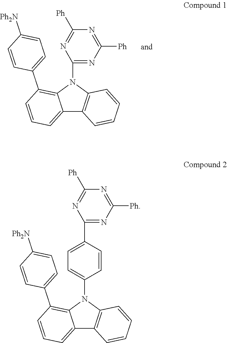
In one preferred embodiment the donor-acceptor compound with a nitrogen containing donor connected to the 1-position of a carbazole and triazene as the acceptor is selected from the group consisting of
##STR00009##
In one embodiment, Ar.sup.1 and Ar.sup.2 in Formula 1 are connected to form a carbazole moiety. In another preferred embodiment, Ar.sup.1 and Ar.sup.2 are connected to form a carbazole moiety and the compound is selected from the group consisting of
##STR00010##
In one embodiment, Ar.sup.2 and Ar.sup.3 in Formula 1 are connected to form a carbazole moiety. In another preferred embodiment, Ar.sup.2 and Ar.sup.3 are connected to form a carbazole moiety and the compound is selected from the group consisting of
##STR00011##
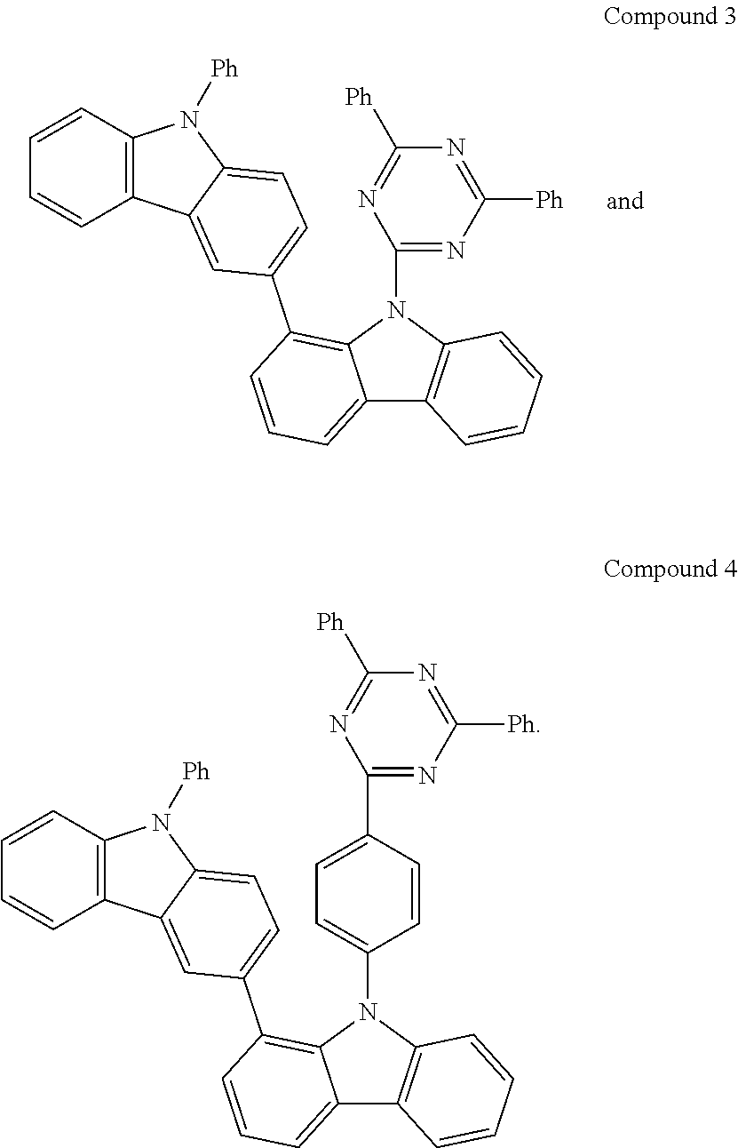
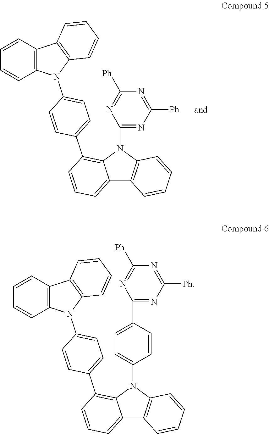
In another preferred embodiment, the compound is selected from the group consisting of
##STR00012## ##STR00013## ##STR00014## ##STR00015## ##STR00016## ##STR00017## ##STR00018## ##STR00019## ##STR00020## ##STR00021## ##STR00022## ##STR00023## ##STR00024##
According to another aspect of the present disclosure, a first device comprising a first organic light emitting device is disclosed. The first organic light emitting device comprises an anode; a cathode; and an emissive layer, disposed between the anode and the cathode, wherein the emissive layer comprises a first emitting compound having a structure according to Formula 1:
##STR00025## wherein R.sup.a to R.sup.g, R.sup.1 and R.sup.2 are independently selected from the group consisting of hydrogen, deuterium, halide, alkyl, cycloalkyl, heteroalkyl, arylalkyl, alkoxy, aryloxy, amino, silyl, alkenyl, cycloalkenyl, heteroalkenyl, alkynyl, aryl, heteroaryl, acyl, carbonyl, carboxylic acids, ester, nitrile, isonitrile, sulfanyl, sulfinyl, sulfonyl, phosphino, and combinations thereof; and wherein Ar.sup.1 to Ar.sup.3 are independently substituted or unsubstituted aryl or heteroaryl and can connect to one another to form fused ring(s) and, wherein L is a direct bond or a linker.
In one embodiment of the first device, the first emitting compound is selected from the group consisting of Compound 1 through Compound 53 disclosed herein.
In one embodiment, the first device emits a luminescent radiation at room temperature when a voltage is applied across the organic light emitting device, wherein the luminescent radiation comprises a delayed fluorescence process.
In one embodiment of the first device, the emissive layer further comprises a first phosphorescent emitting material. In another embodiment, the emissive layer further comprises a second phosphorescent emitting material. In another embodiment, the emissive layer further comprises a host material.
In one embodiment of the first device, the emissive layer further comprises a first phosphorescent emitting material and the first device emits a white light at room temperature when a voltage is applied across the organic light emitting device.
In another embodiment of the first device, the emissive layer further comprises a first phosphorescent emitting material and the first device emits a white light at room temperature when a voltage is applied across the organic light emitting device, and the first emitting compound emits a blue light with a peak wavelength of about 400 nm to about 500 nm.
In another embodiment of the first device, the emissive layer further comprises a first phosphorescent emitting material and the first device emits a white light at room temperature when a voltage is applied across the organic light emitting device, and the first emitting compound emits a yellow light with a peak wavelength of about 530 nm to about 580 nm.
In another embodiment of the first device, the first device comprises a second organic light emitting device, wherein the second organic light emitting device is stacked on the first organic light emitting device.
In one embodiment of the first device, the first device is a consumer product. In another embodiment of the first device, the first device is a lighting panel.
According to another aspect, a formulation comprising a compound having a structure according to Formula 1 is also disclosed.
Synthesis of Compound 1
##STR00026##
1-bromo-9-(4,6-diphenyl-13,5-triazin-2-yl)-9H-carbazole (0.50 g, 1.05 mmol), (4-(diphenylamino)phenyl)boronic acid (0.46 g, 1.26 mmol) and Pd.sub.2(dba).sub.3 (0.03 g) were mixed in a 25 mL two-neck flask. The whole system was evacuated and purged with argon gas. The mixture was dissolved in dry toluene (10 mL). .sup.tBu.sub.3P (2.51 mL, 0.05 M in toluene) and degassed K.sub.2CO.sub.3 (1.26 mL, 2.5 M in H.sub.2O) were added. The mixture was refluxed under argon for 14 hours. After completion of the reaction, it was cooled to room temperature and the mixture was extracted with dichloromethane. The combined organic layer was washed with brine and dried over MgSO.sub.4 after which the solvent was removed by rotary evaporation. The crude product was purified by column chromatography on silica gel using hexane:dichloromethane=5:1 and then with hexane:dichloromethane:toluene=3:1:0.1 to obtained the pure product, Compound 1, (0.60 g, 90%) as a yellow solid.
Synthesis of Compound 2
##STR00027## 1-bromo-9H-carbazole (0.50 g, 2.03 mmol), 4-(diphenylamino)phenylboronic acid (0.71 g, 2.44 mmol), and Pd.sub.2(dba).sub.3 (0.06 g) were mixed in a 25 mL two-neck bottle. The whole system was evacuated and purged with argon gas. Dry toluene (10 mL), t-Bu.sub.3P (4.88 mL of 0.05 M in toluene and degassed K.sub.2CO.sub.3 (3.66 mL, 2.5 M in H.sub.2O) were added. The system was refluxed for 14 hours under an inert atmosphere. Upon completion of the reaction, the mixture was cooled to room temperature and then extracted with ethyl ether. The combined organic layer was washed with brine, dried with MgSO.sub.4 and finally the solvent was removed by rotary evaporation. The crude product was purified by column chromatography on silica gel using hexane:dichloromethane=3:1 as the eluent to obtain the desired product, 4-(9H-carbazol-1-yl)-N,N-diphenylaniline, (0.75 g, 90%) as a white solid.
##STR00028## 4-(9H-carbazol-1-yl)-N,N-diphenylaniline (0.50 g, 1.22 mmol), 2-(4-bromophenyl)-4,6-diphenyl-1,3,5-triazine (0.57 g, 1.46 mmo), Pd.sub.2(dba).sub.3 (0.03 g), and NaO.sup.tBu (0.15 g, 1.58 mmol) were mixed in a 50 mL two neck round bottom flask and the system was evacuated then purged with argon gas. The mixture was dissolved in dry toluene (20 mL). .sup.tBu.sub.3P (2.44 mL, 0.05 M in toluene) was added and the mixture was refluxed under argon for 4 hour. After completion of the reaction, it was cooled to room temperature, the salts were filtered. After removal of the solvent by the rotary evaporation, about 10 mL of dichloromethane was added to the crude product and heated to dissolve of the compound. Hexane was added for crystallization to take place. The solid was filtered and washed with hexane to afford the product, Compound 2, (0.71 g, 81%) as a yellow green solid.
Synthesis of Compound 3
##STR00029## 1-bromo-9-(4,6-diphenyl-1,3,5-triazin-2-yl)-9H-carbazole (0.50 g, 1.05 mmol), 9-phenyl-3-(4,4,5,5-tetramethyl-1,3,2-dioxaborolan-2-yl)-9H-carbazole (0.46 g, 1.26 mmol), and Pd.sub.2(dba).sub.3 (0.03 g) were mixed in a 25 mL two-neck flask, evacuated and then recharged with argon. The mixture was dissolved in dry toluene (10 mL) and then .sup.tBu.sub.3P (2.51 mL, 0.05 M in toluene, 12 mmol) and degassed K.sub.2CO.sub.3 (1.26 mL, 2.5 M in H.sub.2O) were added. The mixture was refluxed under argon for 14 hours. Upon completion of the reaction, the mixture was cooled to room temperature and extracted with dichloromethane. The combined organic layer was wash with brine, dried over MgSO.sub.4 and the solvent was removed by rotary evaporation. The crude product was purified by column chromatography on silica gel using hexane:dichloromethane=5:1, and then changed with hexane:dichloromethane:toluene=3:1:0.1 to obtained pure product, Compound 3, (0.60 g, 90%) as a yellow solid.
Synthesis of Compound 5
##STR00030## A solution containing 9-(4-(4,4,5,5-tetramethyl-1,3,2-dioxaborolan-2-yl)phenyl)-9H-carbazole (0.65 g, 1.8 mmol), Pd(PPh.sub.3).sub.4 (0.09 g, 0.08 mmol), .sup.tBu.sub.3P (3.2 mL of 0.05 M in toluene), 1-bromo-9-(4,6-diphenyl-1,3,5-triazin-2-yl)-9H-carbazole (0.76 mg, 1.6 mmol) and Na.sub.2CO.sub.3 (2.9 mL, 2M in H.sub.2O) in toluene (30 mL) was refluxed with vigorous stirring for 24 hours under an argon atmosphere. The mixture was poured into water and extracted with DCM. The organic extracts were washed with brine and dried over MgSO.sub.4. The solvent was removed by rotary evaporation, and washed with hot DCM to afford the pure product, Compound 5, (0.45 g, 39%).
Table 1 below summarizes the photoluminescence (PL), photoluminescence quantum yield PLQY and solvatochromism data of Compounds 1 and 2. It can be seen that in thin films (5% of emitter by weight in PMMA, mCBP or mCP as host), PLQY's in the range of 50% were obtained. Significant red shift in PL was observed as the solvent polarity increased, indicating the charge transfer origin of the luminescence.
TABLE-US-00001 TABLE 1 PL, PLQY and solvatochromism of Compound 1 and 2. Em.sub.max PLQY Compound Host (nm) (%) Solution Em.sub.max (nm) Compound 1 PMMA 509 57 hexane 504 toluene 530 chloroform 572 Compound 2 PMMA 498 47 3- 490 methylpentane mCBP 496 55 toluene 520 mCP 499 57 2-methylTHF 552
DEVICE EXAMPLES
In the OLED experiment, all device examples were fabricated by high vacuum (<10.sup.7 Torr) thermal evaporation. The anode electrode is .about.800 .ANG. of indium tin oxide (ITO). The cathode consisted of 10 .ANG. of LiF followed by 1,000 .ANG. of Al. All devices were encapsulated with a glass lid sealed with an epoxy resin in a nitrogen glove box (<1 ppm of H.sub.2O and O.sub.2) and a moisture getter was incorporated inside the package.
Device Example 1: The organic stack of the Device Examples consists of sequentially, from the ITO surface, 200 .ANG. of TAPC the hole transporting layer (HTL), 300 .ANG. of Compound A doped with 5% of the emitter Compound 1 as the emissive layer (EML) and 400 .ANG. of TmPyPB as the ETL. Device Example 1 has an external quantum efficiency (EQE) of 12% at 5 cd/m.sup.2 and 7.7% at 1000 cd/m.sup.2. The CIE is 0.249, 0.481, with an emission peak at 502 nm.
The photoluminescence quantum yield (PLQY) of the neat film of Compound 1 was measured to be 57% in Compound 1 in PMMA film (5% by weight). For a standard fluorescent OLED with only prompt singlet emission, the ratio of singlet excitons should be 25%. The outcoupling efficiency of a bottom-emitting lambertian OLED is considered to be around 20-25%. Therefore, for a fluorescent emitter having a PLQY of 57% without additional radiative channels such as delayed fluorescence, the highest EQE should not exceed 3.6% based on the statistical ratio of 25% electrically generated singlet excitons and outcoupling efficiency of 25%. Thus devices containing compounds of Formula I as the emitter, such as Compound 1, showed EQE far exceeding the theoretic limit.
Device Example 2: The organic stack of the Device Examples consists of sequentially, from the ITO surface, 100 .ANG. of LG101 (purchased from LG Chem, Korea) as the hole injection layer (HIL), 300 .ANG. of Compound B the hole transporting layer (HTL), 300 .ANG. of mCBP doped with 6% of the emitter Compound 2 as the emissive layer (EML), 50 .ANG. of Compound C as ETL1 and 400 .ANG. of Compound D as ETL2. Device Example 2 has an EQE of 10% at 1 cd/m.sup.2 and 7.1% at 1000 cd/m.sup.2. The CIE is 0.240, 0.496, with an emission peak at 510 nm. Again, the device EQE far exceeded the conventional fluorescent device efficiency limit.
The chemical structure of the compounds used in the device examples are shown below:
##STR00031## Combination with Other Materials
The materials described herein as useful for a particular layer in an organic light emitting device may be used in combination with a wide variety of other materials present in the device. For example, emissive dopants disclosed herein may be used in conjunction with a wide variety of hosts, transport layers, blocking layers, injection layers, electrodes and other layers that may be present. The materials described or referred to below are non-limiting examples of materials that may be useful in combination with the compounds disclosed herein, and one of skill in the art can readily consult the literature to identify other materials that may be useful in combination.
HIL/HTL:
A hole injecting/transporting material to be used in the present invention is not particularly limited, and any compound may be used as long as the compound is typically used as a hole injecting/transporting material. Examples of the material include, but not limit to: a phthalocyanine or porphyrin derivative; an aromatic amine derivative; an indolocarbazole derivative; a polymer containing fluorohydrocarbon; a polymer with conductivity dopants; a conducting polymer, such as PEDOT/PSS; a self-assembly monomer derived from compounds such as phosphonic acid and silane derivatives; a metal oxide derivative, such as MoO.sub.x; a p-type semiconducting organic compound, such as 1,4,5,8,9,12-Hexaazatriphenylenehexacarbonitrile; a metal complex, and a cross-linkable compounds.
Examples of aromatic amine derivatives used in HIL or HTL include, but not limit to the following general structures:
##STR00032##
Each of Ar.sup.1 to Ar.sup.9 is selected from the group consisting aromatic hydrocarbon cyclic compounds such as benzene, biphenyl, triphenyl, triphenylene, naphthalene, anthracene, phenalene, phenanthrene, fluorene, pyrene, chrysene, perylene, azulene; group consisting aromatic heterocyclic compounds such as dibenzothiophene, dibenzofuran, dibenzoselenophene, furan, thiophene, benzofuran, benzothiophene, benzoselenophene, carbazole, indolocarbazole, pyridylindole, pyrrolodipyridine, pyrazole, imidazole, triazole, oxazole, thiazole, oxadiazole, oxatriazole, dioxazole, thiadiazole, pyridine, pyridazine, pyrimidine, pyrazine, triazine, oxazine, oxathiazine, oxadiazine, indole, benzimidazole, indazole, indoxazine, benzoxazole, benzisoxazole, benzothiazole, quinoline, isoquinoline, cinnoline, quinazoline, quinoxaline, naphthyridine, phthalazine, pteridine, xanthene, acridine, phenazine, phenothiazine, phenoxazine, benzofuropyridine, furodipyridine, benzothienopyridine, thienodipyridine, benzoselenophenopyridine, and selenophenodipyridine; and group consisting 2 to 10 cyclic structural units which are groups of the same type or different types selected from the aromatic hydrocarbon cyclic group and the aromatic heterocyclic group and are bonded to each other directly or via at least one of oxygen atom, nitrogen atom, sulfur atom, silicon atom, phosphorus atom, boron atom, chain structural unit and the aliphatic cyclic group. Wherein each Ar is further substituted by a substituent selected from the group consisting of hydrogen, deuterium, halide, alkyl, cycloalkyl, heteroalkyl, arylalkyl, alkoxy, aryloxy, amino, silyl, alkenyl, cycloalkenyl, heteroalkenyl, alkynyl, aryl, heteroaryl, acyl, carbonyl, carboxylic acids, ester, nitrile, isonitrile, sulfanyl, sulfinyl, sulfonyl, phosphino, and combinations thereof.
In one aspect, Ar.sup.1 to Ar.sup.9 is independently selected from the group consisting of:
##STR00033## wherein k is an integer from 1 to 20; X.sup.101 to X.sup.108 is C (including CH) or N; Z.sup.101 is NAr.sup.1, O, or S; Ar.sup.1 has the same group defined above.
Examples of metal complexes used in HIL or HTL include, but not limit to the following general formula:
##STR00034## wherein Met is a metal, which can have an atomic weight greater than 40; (Y.sup.101-Y.sup.102) is a bidentate ligand, Y.sup.101 and Y.sup.102 are independently selected from C, N, O, P, and S; L.sup.101 is an ancillary ligand; k' is an integer value from 1 to the maximum number of ligands that may be attached to the metal; and k'+k'' is the maximum number of ligands that may be attached to the metal.
In one aspect, (Y.sup.101-Y.sup.102) is a 2-phenylpyridine derivative. In another aspect, (Y.sup.101 Y.sup.102) is a carbene ligand. In another aspect, Met is selected from Ir, Pt, Os, and Zn. In a further aspect, the metal complex has a smallest oxidation potential in solution vs. Fc.sup.+/Fc couple less than about 0.6 V.
Host:
The light emitting layer of the organic EL device of the present invention preferably contains at least a metal complex as light emitting material, and may contain a host material using the metal complex as a dopant material. Examples of the host material are not particularly limited, and any metal complexes or organic compounds may be used as long as the triplet energy of the host is larger than that of the dopant. While the Table below categorizes host materials as preferred for devices that emit various colors, any host material may be used with any dopant so long as the triplet criteria is satisfied.
Examples of metal complexes used as host are preferred to have the following general formula:
##STR00035## wherein Met is a metal; (Y.sup.103-Y.sup.104) is a bidentate ligand, Y.sup.103 and Y.sup.104 are independently selected from C, N, O, P, and S; L.sup.101 is an another ligand; k' is an integer value from 1 to the maximum number of ligands that may be attached to the metal; and k'+k'' is the maximum number of ligands that may be attached to the metal.
In one aspect, the metal complexes are:
##STR00036## wherein (O--N) is a bidentate ligand, having metal coordinated to atoms O and N.
In another aspect, Met is selected from Ir and Pt. In a further aspect, (Y.sup.103-Y.sup.104) is a carbene ligand.
Examples of organic compounds used as host are selected from the group consisting aromatic hydrocarbon cyclic compounds such as benzene, biphenyl, triphenyl, triphenylene, naphthalene, anthracene, phenalene, phenanthrene, fluorene, pyrene, chrysene, perylene, azulene; group consisting aromatic heterocyclic compounds such as dibenzothiophene, dibenzofuran, dibenzoselenophene, furan, thiophene, benzofuran, benzothiophene, benzoselenophene, carbazole, indolocarbazole, pyridylindole, pyrrolodipyridine, pyrazole, imidazole, triazole, oxazole, thiazole, oxadiazole, oxatriazole, dioxazole, thiadiazole, pyridine, pyridazine, pyrimidine, pyrazine, triazine, oxazine, oxathiazine, oxadiazine, indole, benzimidazole, indazole, indoxazine, benzoxazole, benzisoxazole, benzothiazole, quinoline, isoquinoline, cinnoline, quinazoline, quinoxaline, naphthyridine, phthalazine, pteridine, xanthene, acridine, phenazine, phenothiazine, phenoxazine, benzofuropyridine, furodipyridine, benzothienopyridine, thienodipyridine, benzoselenophenopyridine, and selenophenodipyridine; and group consisting 2 to 10 cyclic structural units which are groups of the same type or different types selected from the aromatic hydrocarbon cyclic group and the aromatic heterocyclic group and are bonded to each other directly or via at least one of oxygen atom, nitrogen atom, sulfur atom, silicon atom, phosphorus atom, boron atom, chain structural unit and the aliphatic cyclic group. Wherein each group is further substituted by a substituent selected from the group consisting of hydrogen, deuterium, halide, alkyl, cycloalkyl, heteroalkyl, arylalkyl, alkoxy, aryloxy, amino, silyl, alkenyl, cycloalkenyl, heteroalkenyl, alkynyl, aryl, heteroaryl, acyl, carbonyl, carboxylic acids, ester, nitrile, isonitrile, sulfanyl, sulfinyl, sulfonyl, phosphino, and combinations thereof.
In one aspect, host compound contains at least one of the following groups in the molecule:
##STR00037## ##STR00038## wherein R.sup.101 to R.sup.107 is independently selected from the group consisting of hydrogen, deuterium, halide, alkyl, cycloalkyl, heteroalkyl, arylalkyl, alkoxy, aryloxy, amino, silyl, alkenyl, cycloalkenyl, heteroalkenyl, alkynyl, aryl, heteroaryl, acyl, carbonyl, carboxylic acids, ester, nitrile, isonitrile, sulfanyl, sulfinyl, sulfonyl, phosphino, and combinations thereof, when it is aryl or heteroaryl, it has the similar definition as Ar's mentioned above. k is an integer from 0 to 20 or 1 to 20; k''' is an integer from 0 to 20. X.sup.101 to X.sup.108 is selected from C (including CH) or N. Z.sup.101 and Z.sup.102 is selected from NR.sup.101, O, or S. HBL:
A hole blocking layer (HBL) may be used to reduce the number of holes and/or excitons that leave the emissive layer. The presence of such a blocking layer in a device may result in substantially higher efficiencies as compared to a similar device lacking a blocking layer. Also, a blocking layer may be used to confine emission to a desired region of an OLED.
In one aspect, compound used in HBL contains the same molecule or the same functional groups used as host described above.
In another aspect, compound used in HBL contains at least one of the following groups in the molecule:
##STR00039## wherein k is an integer from 1 to 20; L.sup.101 is an another ligand, k' is an integer from 1 to 3. ETL:
Electron transport layer (ETL) may include a material capable of transporting electrons. Electron transport layer may be intrinsic (undoped), or doped. Doping may be used to enhance conductivity. Examples of the ETL material are not particularly limited, and any metal complexes or organic compounds may be used as long as they are typically used to transport electrons.
In one aspect, compound used in ETL contains at least one of the following groups in the molecule:
##STR00040## wherein R.sup.101 is selected from the group consisting of hydrogen, deuterium, halide, alkyl, cycloalkyl, heteroalkyl, arylalkyl, alkoxy, aryloxy, amino, silyl, alkenyl, cycloalkenyl, heteroalkenyl, alkynyl, aryl, heteroaryl, acyl, carbonyl, carboxylic acids, ester, nitrile, isonitrile, sulfanyl, sulfinyl, sulfonyl, phosphino, and combinations thereof, when it is aryl or heteroaryl, it has the similar definition as Ar's mentioned above. Ar.sup.1 to Ar.sup.3 has the similar definition as Ar's mentioned above. k is an integer from 1 to 20. X.sup.101 to X.sup.108 is selected from C (including CH) or N.
In another aspect, the metal complexes used in ETL contains, but not limit to the following general formula:
##STR00041## wherein (O--N) or (N--N) is a bidentate ligand, having metal coordinated to atoms O, N or N, N; L.sup.101 is another ligand; k' is an integer value from 1 to the maximum number of ligands that may be attached to the metal.
In any above-mentioned compounds used in each layer of the OLED device, the hydrogen atoms can be partially or fully deuterated. Thus, any specifically listed substituent, such as, without limitation, methyl, phenyl, pyridyl, etc. encompasses undeuterated, partially deuterated, and fully deuterated versions thereof. Similarly, classes of substituents such as, without limitation, alkyl, aryl, cycloalkyl, heteroaryl, etc. also encompass undeuterated, partially deuterated, and fully deuterated versions thereof.
In addition to and/or in combination with the materials disclosed herein, many hole injection materials, hole transporting materials, host materials, dopant materials, exiton/hole blocking layer materials, electron transporting and electron injecting materials may be used in an OLED. Non-limiting examples of the materials that may be used in an OLED in combination with materials disclosed herein are listed in Table A below. Table A lists non-limiting classes of materials, non-limiting examples of compounds for each class, and references that disclose the materials.
TABLE-US-00002 TABLE A MATERIAL EXAMPLES OF MATERIAL PUBLICATIONS Hole injection materials Phthalocyanine and porphryin compounds ##STR00042## Appl. Phys. Lett. 69, 2160 (1996) Starburst triarylamines ##STR00043## J. Lumin. 72-74, 985 (1997) CF.sub.x Fluorohydrocarbon polymer ##STR00044## Appl. Phys. Lett. 78, 673 (2001) Conducting polymers (e.g., PEDOT:PSS, polyaniline, polythiophene) ##STR00045## Synth. Met. 87, 171 (1997) WO2007002683 Phosphonic acid and sliane SAMs ##STR00046## US20030162053 Triarylamine or polythiophene polymers with conductivity dopants ##STR00047## EP1725079A1 ##STR00048## ##STR00049## Organic compounds with conductive inorganic compounds, such as molybdenum and tungsten oxides ##STR00050## US20050123751 SID Symposium Digest, 37, 923 (2006 WO2009018009 n-type semiconducting organic complexes ##STR00051## US20020158242 Metal organometallic complexes ##STR00052## US20060240279 Cross-linkable compounds ##STR00053## US20080220265 Polythiophene based polymers and copolymers ##STR00054## WO 2011075644 EP2350216 Hole transporting materials Triarylamines (e.g., TPD, .alpha.-NPD) ##STR00055## Appl. Phys. Lett. 51, 913 (3987) ##STR00056## U.S. Pat. No. 5,061,569 ##STR00057## EP650955 ##STR00058## J. Mater. Chem. 3, 319 (1993) ##STR00059## Appl. Phys. Lett. 90, 183503 (2007) ##STR00060## Appl. Phys. Lett. 90, 183503 (2007) Triarylamine on spirofluorene core ##STR00061## Synth. Met. 91, 209 (1997) Arylamine carbazole compounds ##STR00062## Adv. Mater. 6, 677 (1994), US20080124572 Triarylamine with (di)benzothiophene/(di) benzofuran ##STR00063## US20070278938, US20080106190 US20110163302 Indolocarbazoles ##STR00064## Synth. Met. 111, 421 (2000) Isoindole compounds ##STR00065## Chem. Mater. 15, 3148 (2003) Metal carbene complexes ##STR00066## US20080018221 Phosphorescent OLED host materials Red hosts Arylcarbazoles ##STR00067## Appl. Phys. Lett. 78, 1622 (2001) Metal 8-hydroxyquinolates (e.g., Alq.sub.3, BAlq) ##STR00068## Nature 395, 151 (1998) ##STR00069## US20060202194 ##STR00070## WO2005014551 ##STR00071## WO2006072002 Metal phenoxyhenzothiazole compounds ##STR00072## Appl. Phys. Lett. 90, 123509 (2007) Conjugated oligomers and polymers (e.g., polyfluorene) ##STR00073## Org. Electron. 1, 15 (2000) Aromatic fused rings ##STR00074## WO2009066779, WO2009066778, WO2009063833, US20090045731, US20090045730, WO2009008311, US20090008605, US20090009065 Zinc complexes ##STR00075## WO2010056066 Chrysene based compounds ##STR00076## WO2011086863 Green hosts Arylcarbazoles ##STR00077## Appl. Phys. Lett. 78, 1622 (2001) ##STR00078## US20030175553 ##STR00079## WO2001039234 Aryltriphenylene compounds ##STR00080## US20060280965 ##STR00081## US20060280965 ##STR00082## WO2009021126 Poly-fused heteroaryl compounds ##STR00083## US20090309488 US20090302743 US20100012931 Donor acceptor type molecules ##STR00084## WO2008056746 ##STR00085## WO2010107244 Aza-carbazole/DBT/DBF ##STR00086## JP2008074939 ##STR00087## US20100187984 Polymers (e.g., PVK) ##STR00088## Appl. Phys. Lett. 77, 2280 (2000) Spirofluorene compounds ##STR00089## WO2004093207 Metal phenoxybenzooxazole compounds ##STR00090## WO2005089025 ##STR00091## WO2006132173 ##STR00092## JP200511610 Spirofluorene-carbazole compounds ##STR00093## JP2007254297 ##STR00094## JP2007254297 Indolocabazoles ##STR00095## WO2007063796 ##STR00096## WO2007063754 5-member ring electron deficient heterocycles (e.g., triazole, oxadiazole) ##STR00097## J. Appl. Phys. 90, 5048 (2001) ##STR00098## WO2004107822 Tetraphenylene complexes ##STR00099## US20050112407 Metal phenoxypyridine compounds ##STR00100## WO2005030900 Metal coordination complexes (e.g., Zn, Al with N{circumflex over ( )}N ligands) ##STR00101## US20040137268, US20040137267 Blue hosts Arylcarbazoles ##STR00102## Appl. Phys. Lett, 82, 2422 (2003) ##STR00103## US20070190359 Dibenzothiophene/ Dibenzofuran-carbazole compounds ##STR00104## WO2006114966, US20090167162 ##STR00105## US20090167162 ##STR00106## WO2009086028 ##STR00107## US20090030202, US20090017330 ##STR00108## US20100084966 Silicon aryl compounds ##STR00109## US20050238919 ##STR00110## WO2009003898 Silicon/Germanium aryl compounds ##STR00111## EP2034538A Aryl benzoyl ester ##STR00112## WO2006100298 Carbazoic linked by non- conjugated groups ##STR00113## US20040115476 Aza-carbazoles ##STR00114## US20060121308 High triplet metal organometallic complex ##STR00115## U.S. Pat. No. 7,154,114 Phosphorescent dopants Red dopants Heavy metal porphyrins (e.g., PtOEP) ##STR00116## Nature 395. 151 (1998) Iridium (III) organometallic complexes ##STR00117## Appl. Phys. Lett. 78, 1622 (2001) ##STR00118## US20030072964 ##STR00119## US20030072964 ##STR00120## US20060202194 ##STR00121## US20060202194 ##STR00122## US20070087321 ##STR00123## US20080261076 US20100090591 ##STR00124## US20070087321 ##STR00125## Adv. Mater. 19, 739 (2007) ##STR00126## WO2009100991 ##STR00127## WO2008101842 ##STR00128## U.S. Pat. No. 7,232,618 Platinum(II) organometallic complexes ##STR00129## WO2003040257 ##STR00130## US20070103060 Osminum(III) complexes ##STR00131## Chem. Mater. i7, 3532 (2005) Ruthenium(II) complexes ##STR00132## Adv. Mater. 17, 1059 (2005) Rhenium (I), (II), and (III) complexes ##STR00133## US20050244673 Green dopants Iridium(III) organometallic complexes ##STR00134## Inorg. Chem. 40, 1704 (2001) ##STR00135## US20020034656 ##STR00136## U.S. Pat. No. 7,332,232 ##STR00137## US20090108737 ##STR00138## WO2010028151 ##STR00139## EP1841834B ##STR00140## US20060127696 ##STR00141## US20090039776 ##STR00142## U.S. Pat. No. 6,921,915 ##STR00143## US20100244004 ##STR00144## U.S. Pat. No. 6,687,266 ##STR00145## Chem. Mater. 16, 2480 (2004) ##STR00146## US20070190359 ##STR00147## US 20060008670 JP2007123392
##STR00148## WO2010086089, WO2011044988 ##STR00149## Adv. Mater. 16, 2003 (2004) ##STR00150## Angew. Chem. Int. Ed. 2006, 45, 7800 ##STR00151## WO2009050290 ##STR00152## US20090165846 ##STR00153## US20080015355 ##STR00154## US20010015432 ##STR00155## US20100295032 Monomer for polymeric metal organometallic compounds ##STR00156## U.S. Pat. No. 7,250,226, U.S. Pat. No. 7,396,598 Pt(II) organometallic complexes, including polydentated ligands ##STR00157## Appl. Phys. Lett. 86, 153505 (2005) ##STR00158## Appl. Phys. Lett. 86, 153505 (2005) ##STR00159## Chem. Lett. 34, 592 (2005) ##STR00160## WO2002015645 ##STR00161## US20060263635 ##STR00162## US20060182992 US20070103060 Cu complexes ##STR00163## WO2009000673 ##STR00164## US20070111026 Gold complexes ##STR00165## Chcm. Commun. 2906 (2005) Rhenium(III) complexes ##STR00166## Inorg. Chcm. 42, 1248 (2003) Osmium(II) complexes ##STR00167## U.S. Pat. No. 7,279,704 Deuterated organometallic complexes ##STR00168## US20030138657 Organometallic complexes with two or more metal centers ##STR00169## US20030152802 ##STR00170## U.S. Pat. No. 7,090,928 Blue dopants Iridium(III) organometallic complexes ##STR00171## WO2002002714 ##STR00172## WO2006009024 ##STR00173## US20060251923 US20110057559 US20110204333 ##STR00174## U.S. Pat. No. 7,393,599, WO2006056418, US20050260441, WO2005019373 ##STR00175## U.S. Pat. No. 7,534,505 ##STR00176## WO2011051404 ##STR00177## U.S. Pat. No. 7,445,855 ##STR00178## US20070190359, US20080297033 US20100148663 ##STR00179## U.S. Pat. No. 7,338,722 ##STR00180## US20020134984 ##STR00181## Angcw. Chem. Int. Ed. 47, 4542 (2008) ##STR00182## Chem. Mater. 18, 5119 (2006) ##STR00183## Inorg. Chem. 46, 4308 (2007) ##STR00184## WO2005123873 ##STR00185## WO2005123873 ##STR00186## WO2007004380 ##STR00187## WO2006082742 Osmium(II) complexes ##STR00188## U.S. Pat. No. 7,279,704 ##STR00189## Organometallics 23, 3745 (2004) Gold complexes ##STR00190## Appl. Phys. Lett. 74, 1361 (1999) Platinum(II) complexes ##STR00191## WO2006098120, WO2006103874 Pt tetradentate complexes with at least one metal- carbene bond ##STR00192## U.S. Pat. No. 7,655,323 Exciton/hole blocking layer materials Bathocuprine compounds (e.g., BCP, BPhen) ##STR00193## Appl. Phys. Lett. 75, 4 (1999) ##STR00194## Appl. Phys. Lett. 79, 449 (2001) Metal 8-hydroxyquinolates (e.g., BAlq) ##STR00195## Appl. Phys. Lett. 81, 162 (2002) 5-member ring electron deficient heterocycles such as triazole, oxadiazole, imidazole benzoimidazole ##STR00196## Appl. Phys. Lett. 81, 162 (2002) Triphenylene compounds ##STR00197## US20050025993 Fluorinated aromatic compounds ##STR00198## Appl. Phys. Lett. 79, 156 (2001) Phenothiazine-S-oxide ##STR00199## WO2008132085 Silylated five-membered nitrogen, oxygen, sulfur or phosphorus dibenzoheterocycles ##STR00200## WO2010079051 Aza-carbazoles ##STR00201## US20060121308 Anthracene- benzoimidazole compounds ##STR00202## WO2003060956 ##STR00203## US20090179554 Aza triphenylene derivatives ##STR00204## US20090115316 Anthracene-benzothiazole compounds ##STR00205## Appl. Phys. Lett. 89, 063504 (2006) Metal 8-hydroxyquinolates (e.g., Alq.sub.3, Zrq.sub.4) ##STR00206## Appl. Phys. Lett. 51, 913 (3987) US7230107 Metal hydroxybenoquinolates ##STR00207## Chem. Lett. 5, 905 (1993) Bathocuprine compounds such as BCP, BPhen, etc ##STR00208## Appl. Phys. Lett. 91, 263503 (2007) ##STR00209## Appl. Phys. Lett. 79, 449 (2001) 5-member ring electron deficient heterocycles (e.g., triazole, oxadiazole, imidazole, benzoimidazole) ##STR00210## Appl. Phys. Lett. 74, 865 (1999) ##STR00211## Appl. Phys. Lett. 55, 1489 (1989) ##STR00212## Jpn. J. Apply. Phys. 32, L917 (1993) Silole compounds ##STR00213## Org. Electron. 4, 113 (2003) Arylborane compounds ##STR00214## J. Am. Chem. Soc. 120, 9714 (1998) Fluorinated aromatic compounds ##STR00215## J. Am. Chem. Soc. 122, 1832 (2000) Fullerene (e.g., C60) ##STR00216## US20090101870 Triazine complexes ##STR00217## US20040036077 Zn (N{circumflex over ( )}N) complexes ##STR00218## U.S. Pat. No. 6,528,187
It is understood that the various embodiments described herein are by way of example only, and are not intended to limit the scope of the invention. For example, many of the materials and structures described herein may be substituted with other materials and structures without deviating from the spirit of the invention. The present invention as claimed may therefore include variations from the particular examples and preferred embodiments described herein, as will be apparent to one of skill in the art. It is understood that various theories as to why the invention works are not intended to be limiting.
* * * * *
C00001
C00002
C00003
C00004
C00005
C00006
C00007
C00008
C00009
C00010
C00011
C00012
C00013
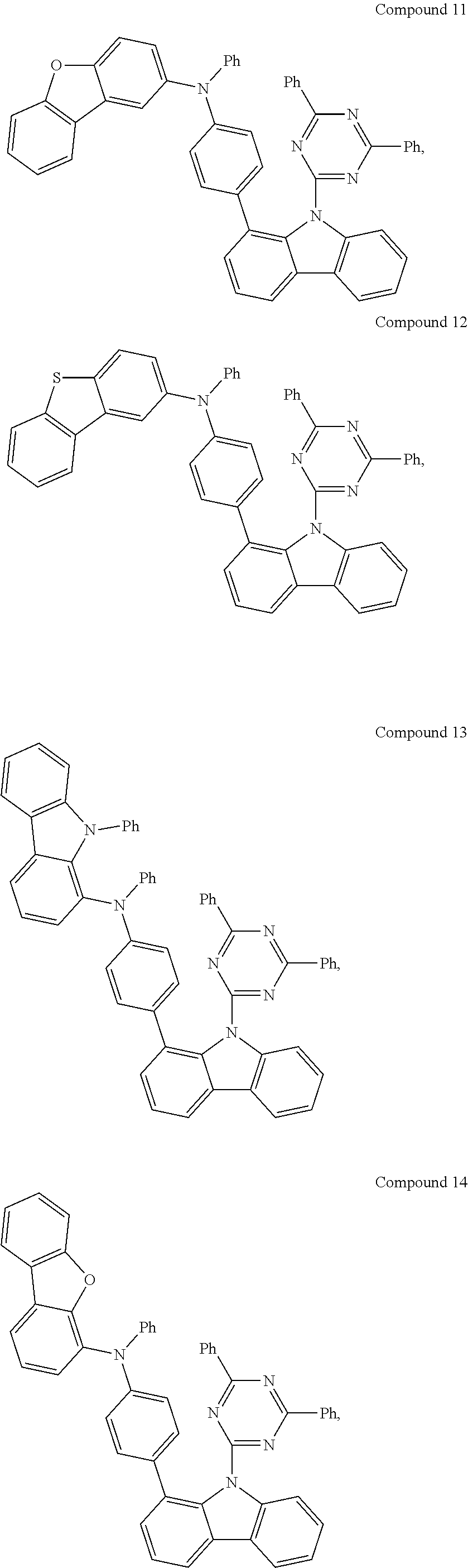
C00014
C00015

C00016
C00017
C00018
C00019

C00020
C00021

C00022
C00023

C00024
C00025
C00026
C00027
C00028
C00029
C00030
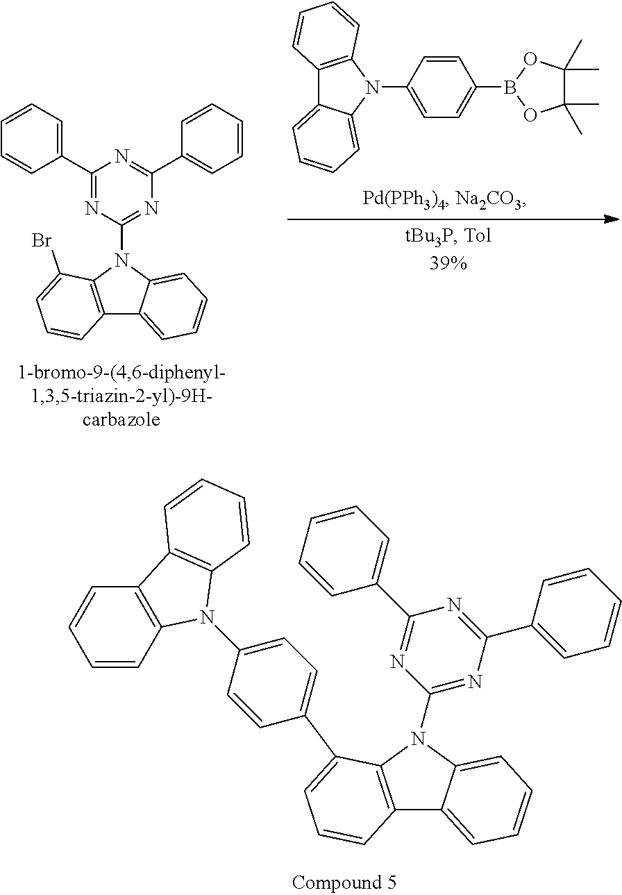
C00031
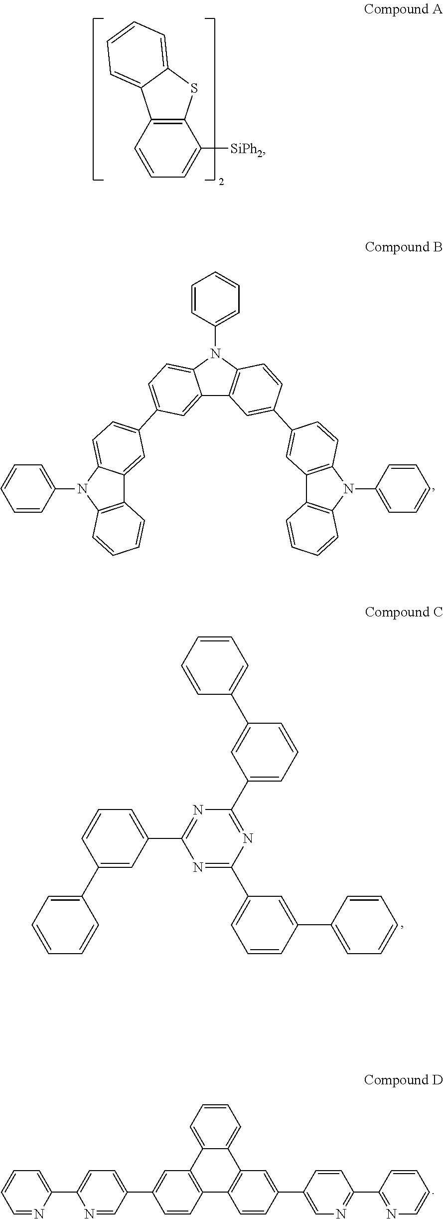
C00032
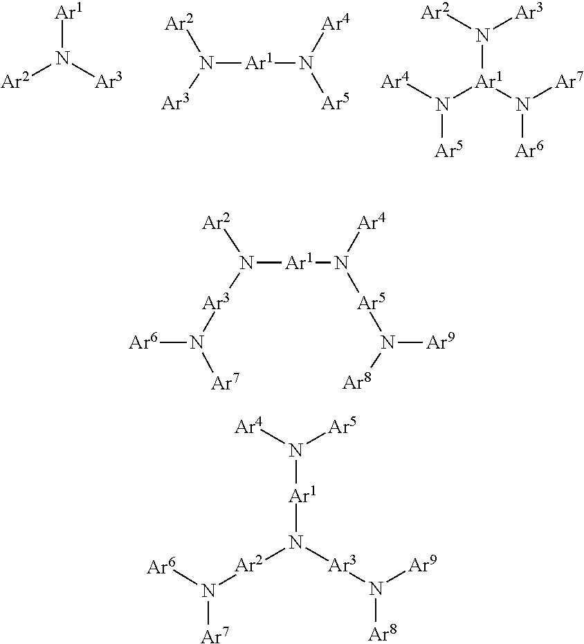
C00033
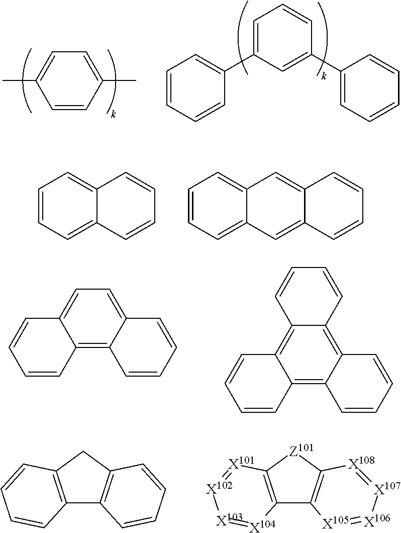
C00034
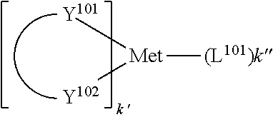
C00035
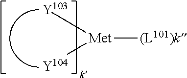
C00036
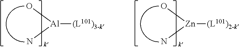
C00037
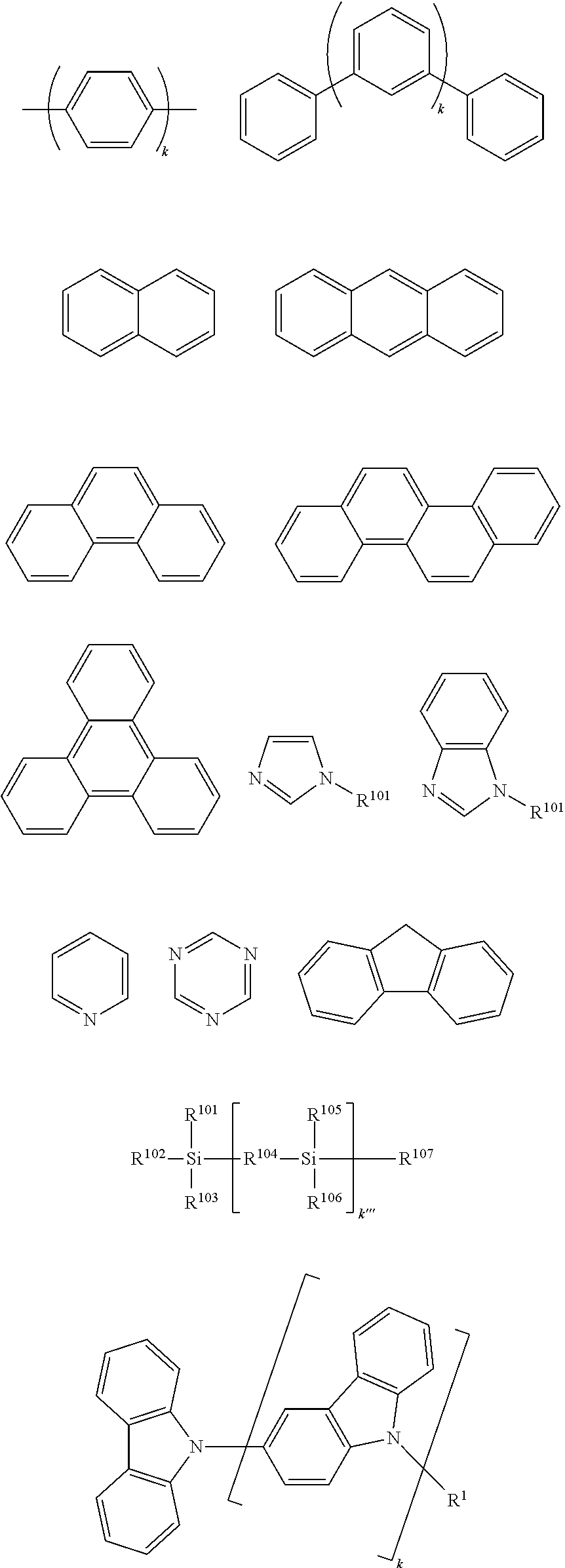
C00038
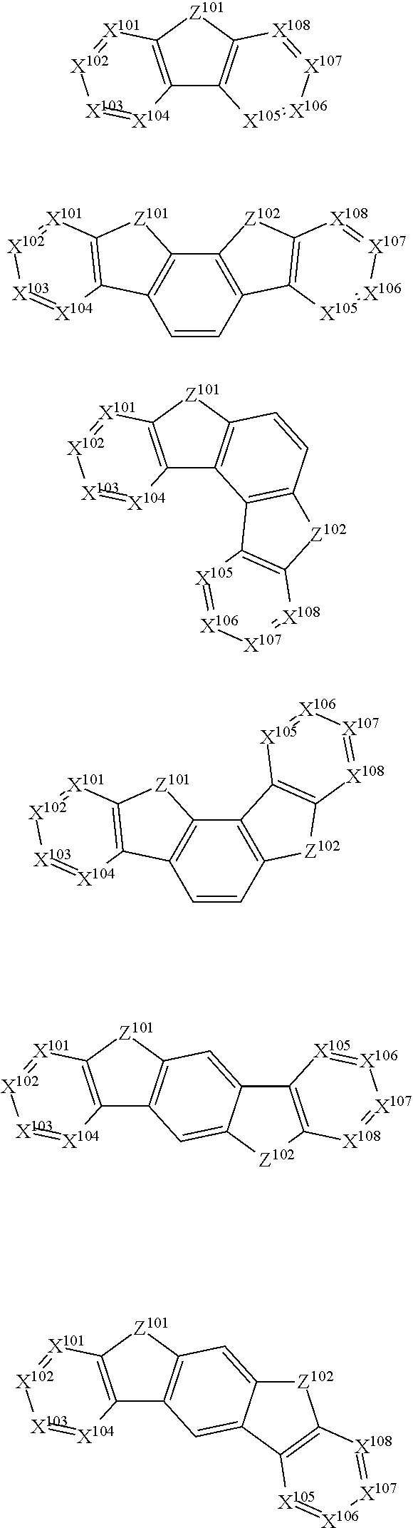
C00039
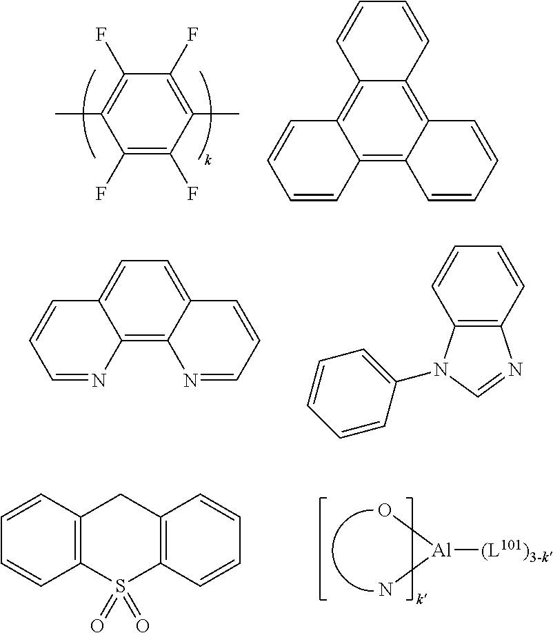
C00040

C00041
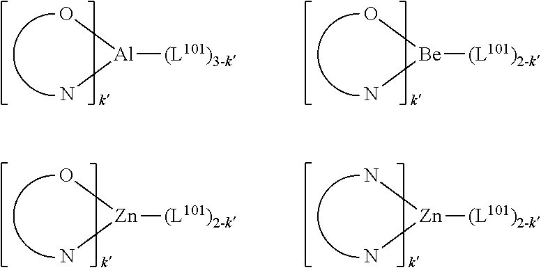
C00042
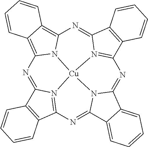
C00043
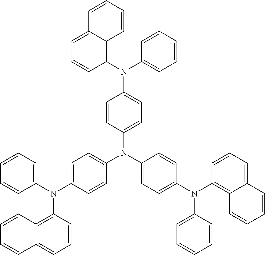
C00044
C00045

C00046
C00047
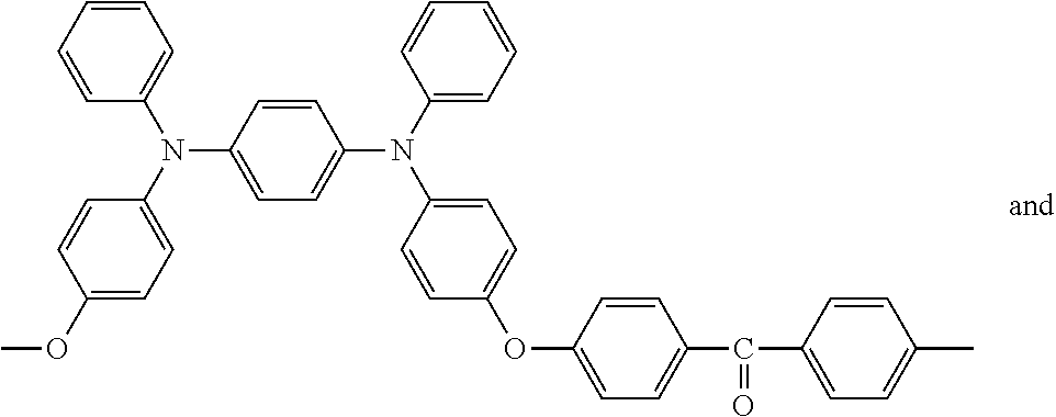
C00048
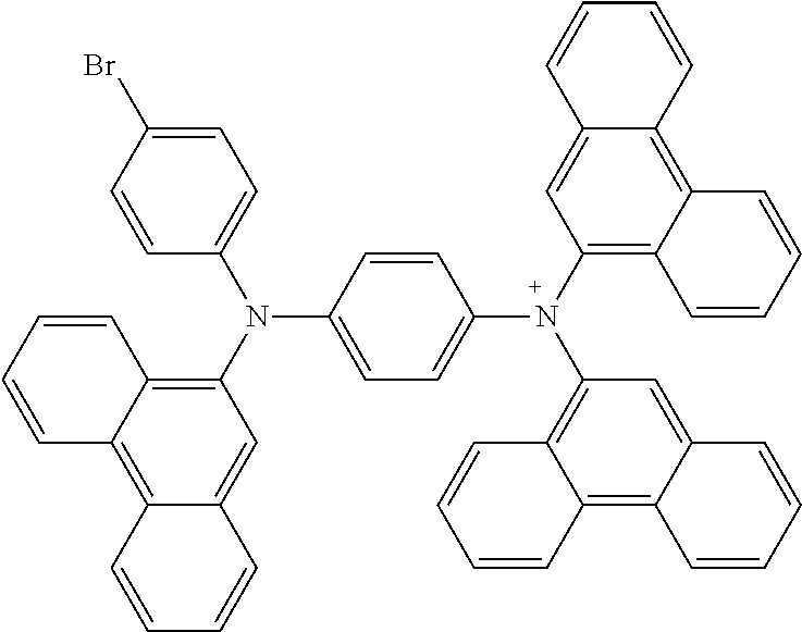
C00049

C00050
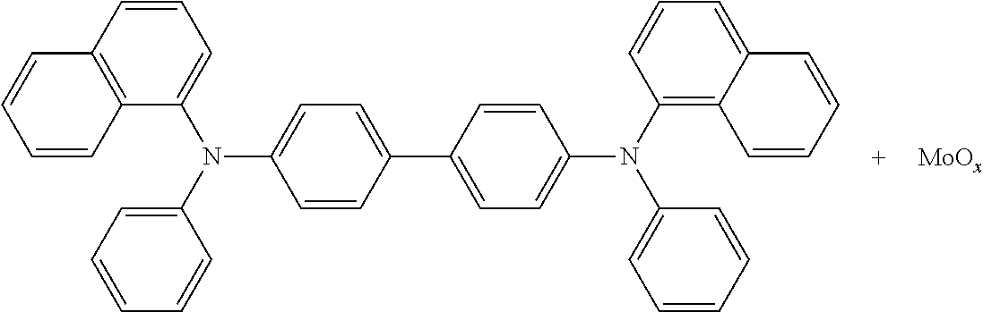
C00051
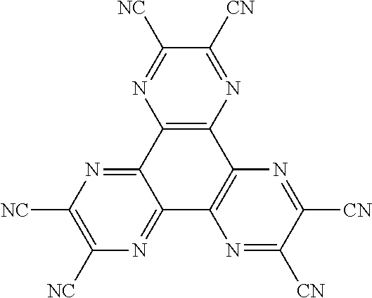
C00052
C00053
C00054
C00055
C00056
C00057
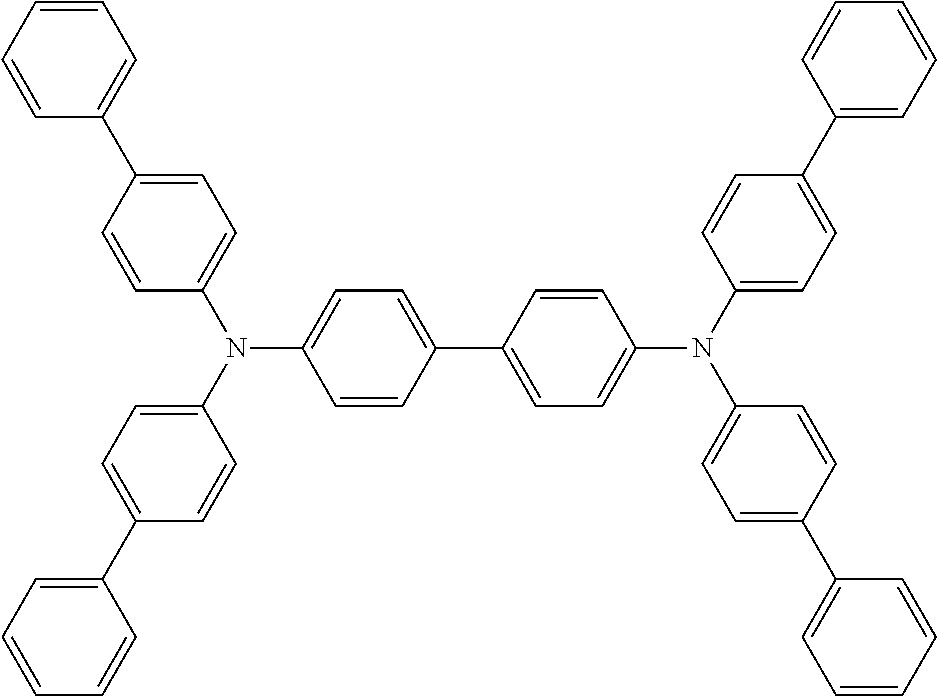
C00058
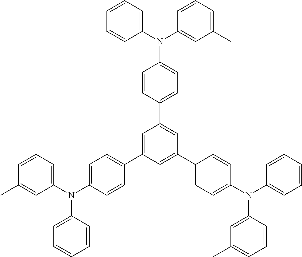
C00059
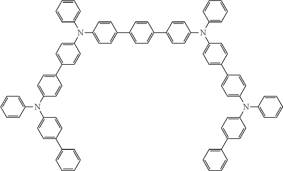
C00060
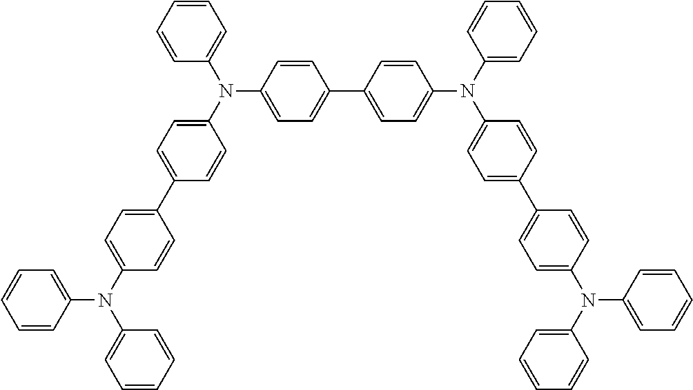
C00061
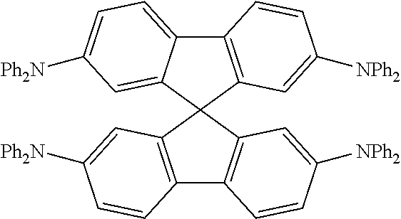
C00062
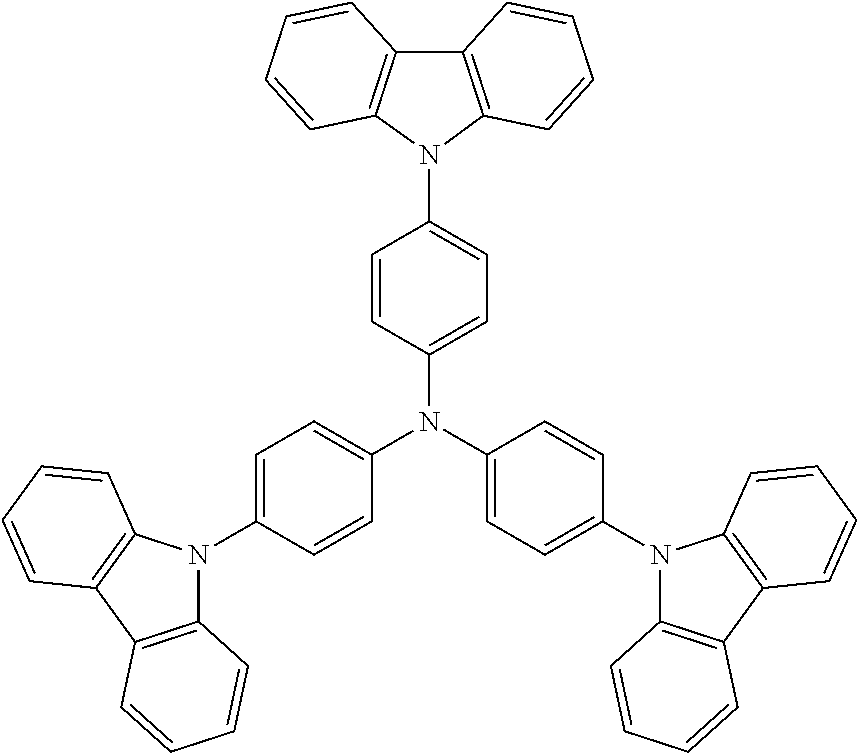
C00063
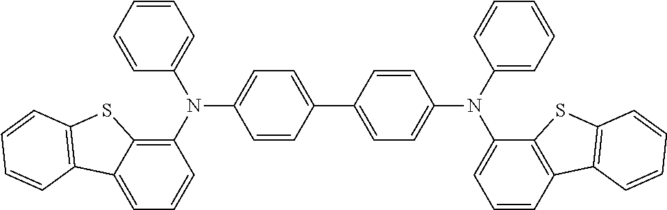
C00064
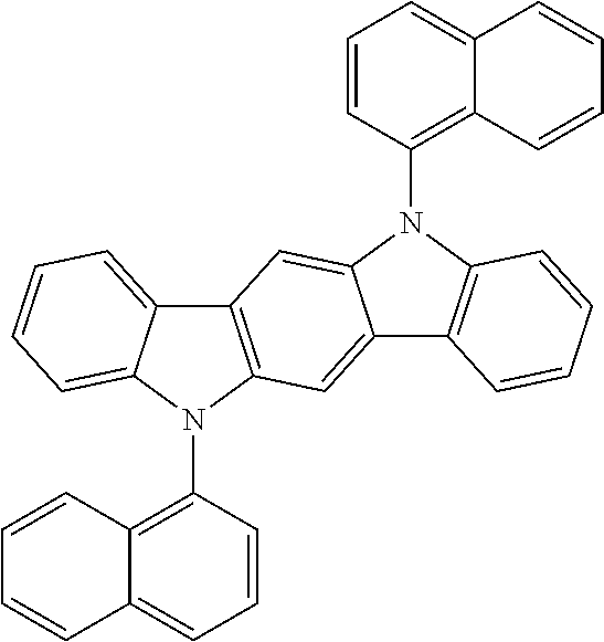
C00065
C00066
C00067
C00068
C00069
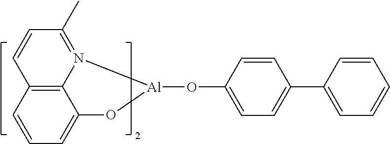
C00070
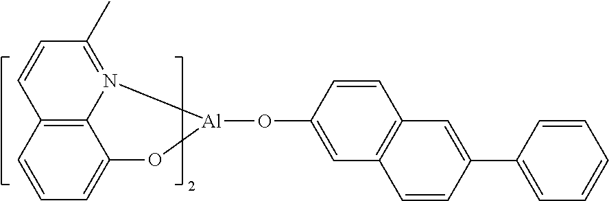
C00071
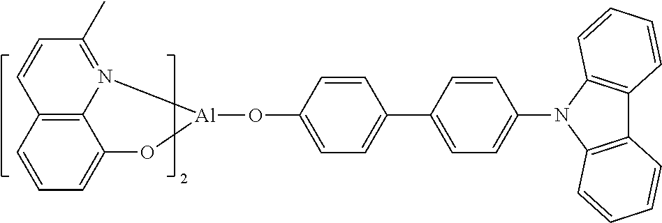
C00072
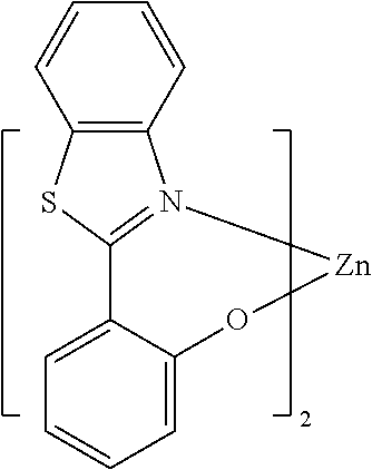
C00073
C00074
C00075
C00076
C00077
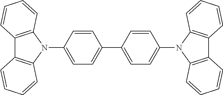
C00078
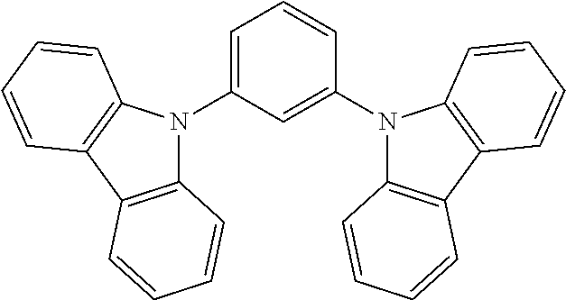
C00079
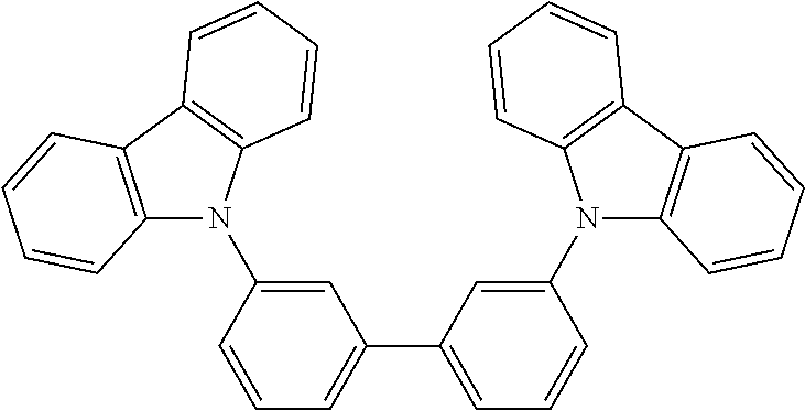
C00080
C00081
C00082
C00083

C00084

C00085
C00086
C00087
C00088
C00089
C00090
C00091
C00092
C00093
C00094
C00095

C00096
C00097
C00098
C00099
C00100
C00101
C00102
C00103
C00104
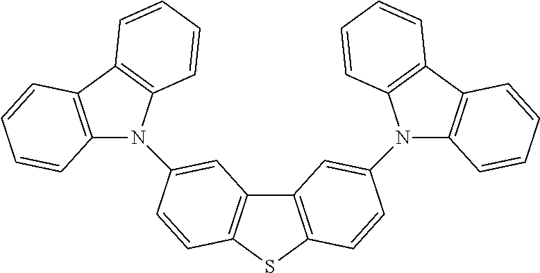
C00105
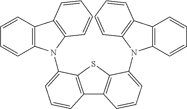
C00106
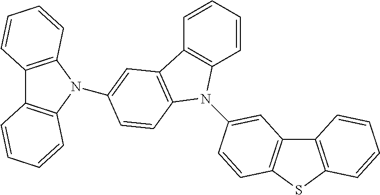
C00107
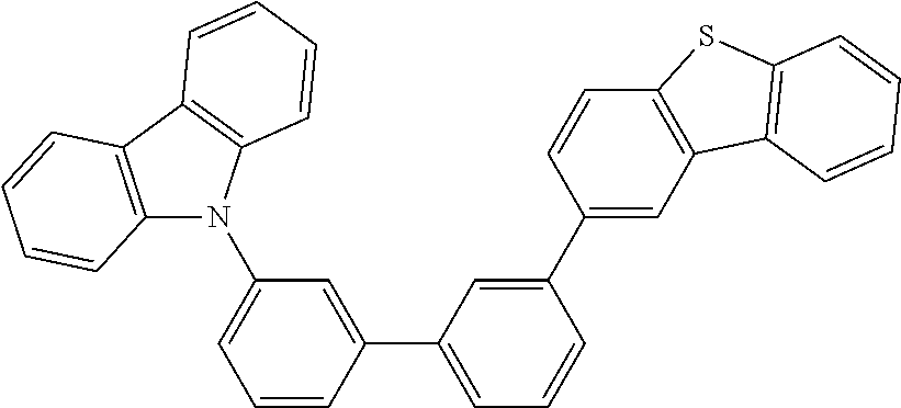
C00108
C00109
C00110
C00111

C00112
C00113
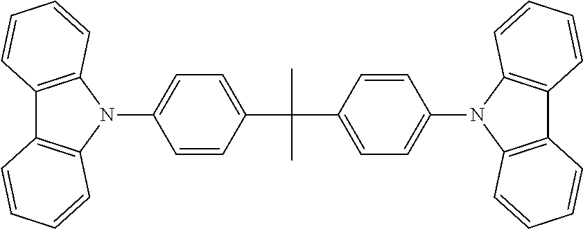
C00114
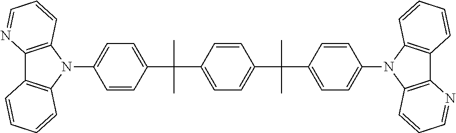
C00115
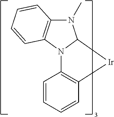
C00116
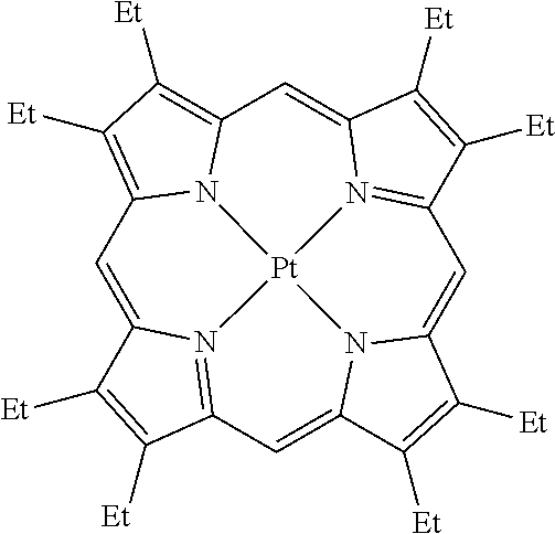
C00117
C00118
C00119
C00120
C00121
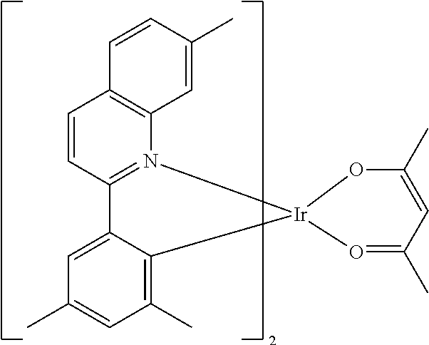
C00122
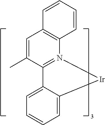
C00123
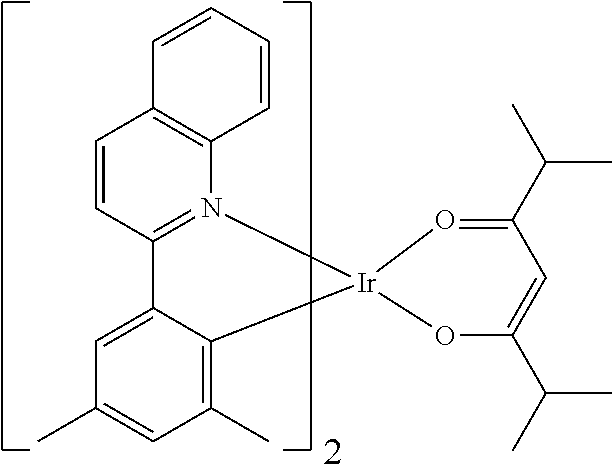
C00124
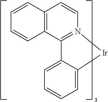
C00125
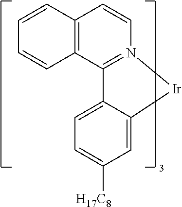
C00126
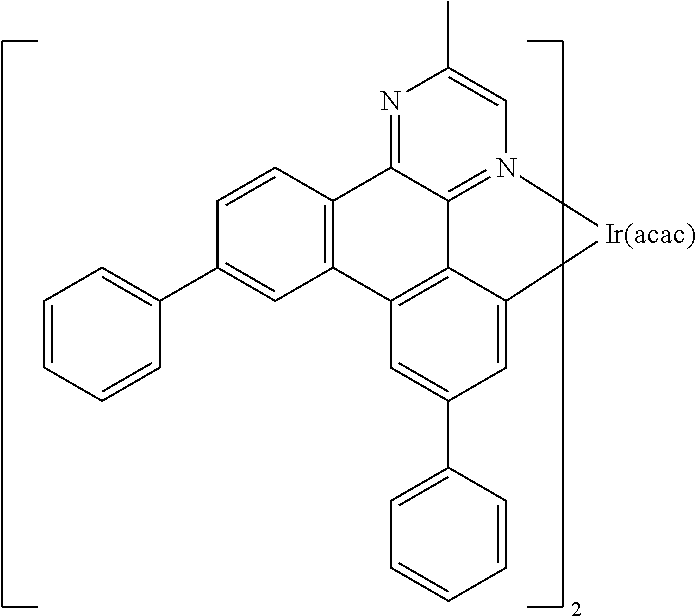
C00127
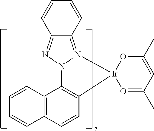
C00128
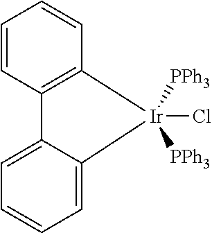
C00129
C00130
C00131
C00132
C00133
C00134
C00135
C00136
C00137
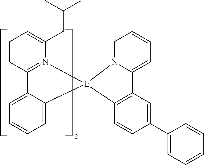
C00138
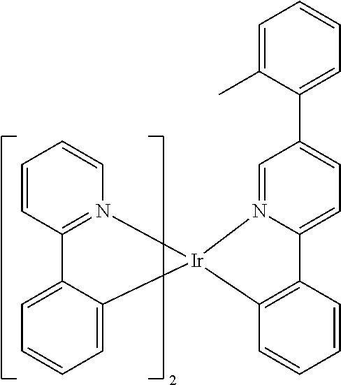
C00139
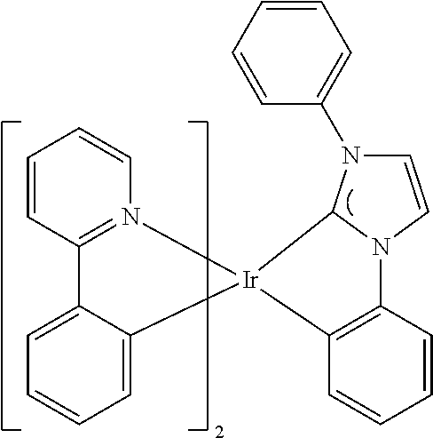
C00140
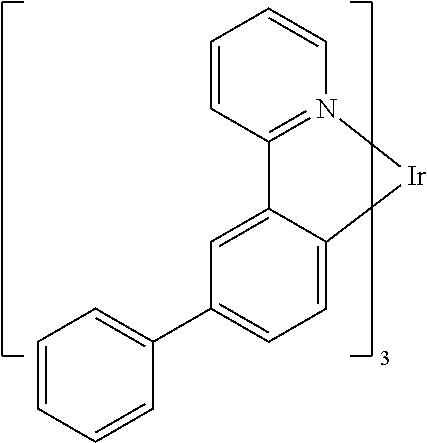
C00141
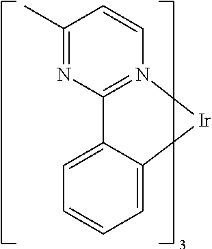
C00142
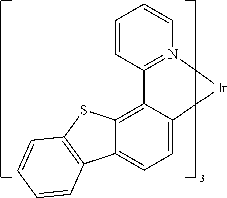
C00143
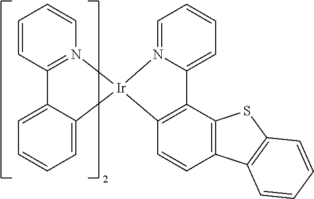
C00144
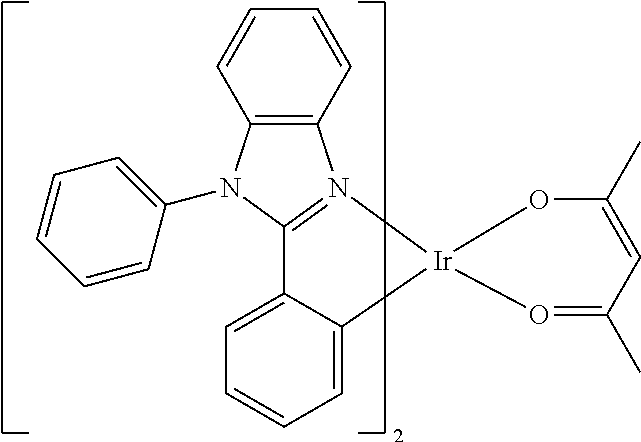
C00145
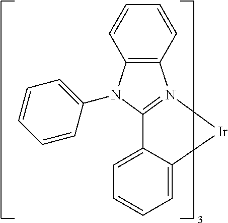
C00146

C00147

C00148

C00149
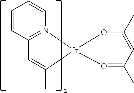
C00150
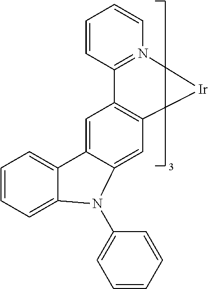
C00151
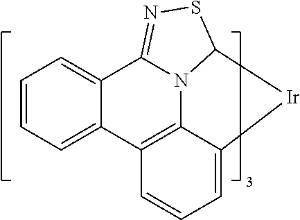
C00152
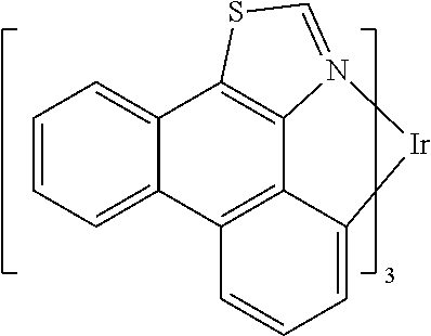
C00153
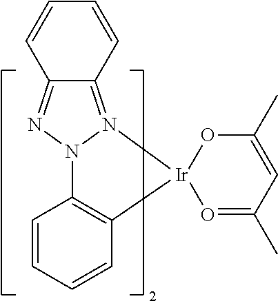
C00154
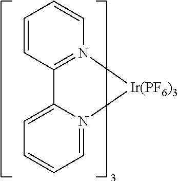
C00155
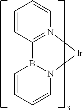
C00156
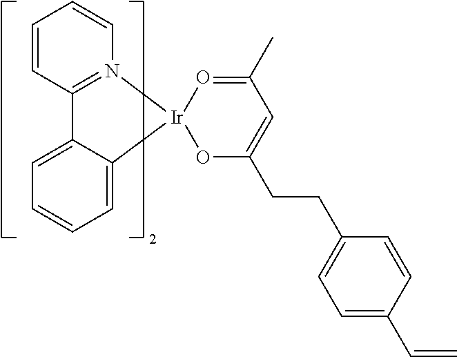
C00157
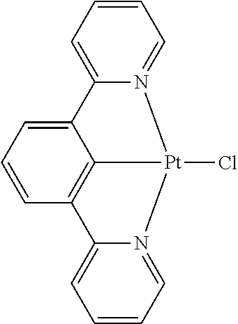
C00158
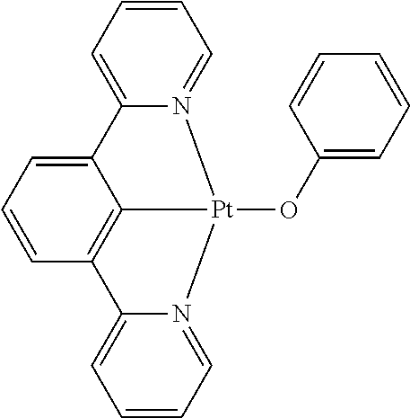
C00159
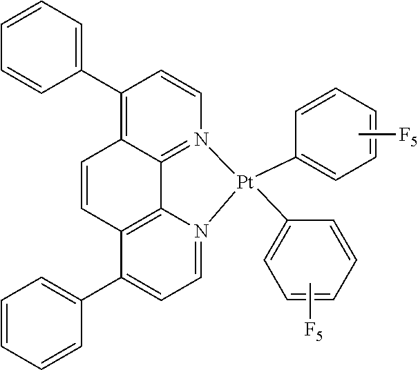
C00160
C00161
C00162
C00163
C00164
C00165
C00166
C00167
C00168
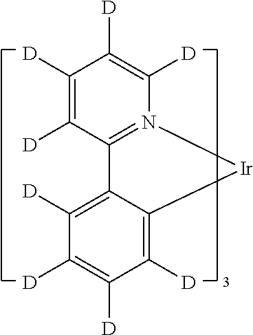
C00169
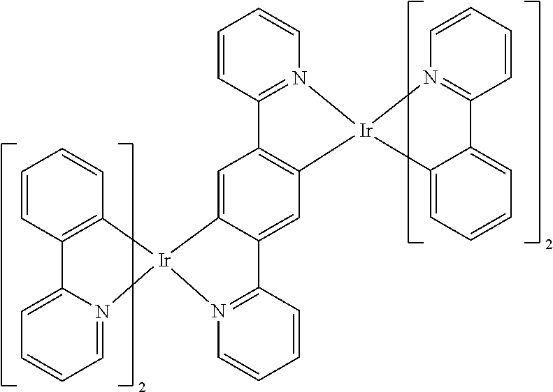
C00170
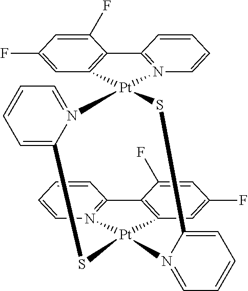
C00171
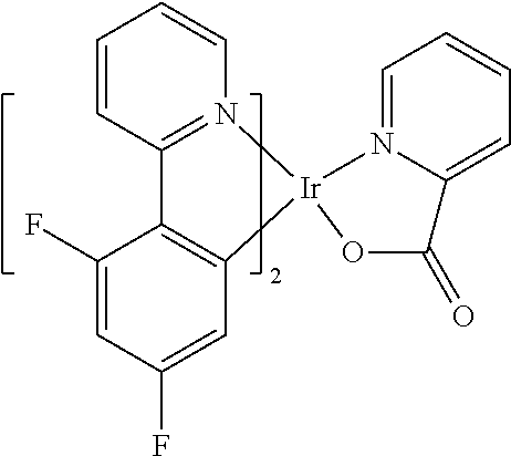
C00172
C00173
C00174
C00175
C00176
C00177
C00178
C00179
C00180
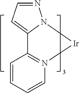
C00181
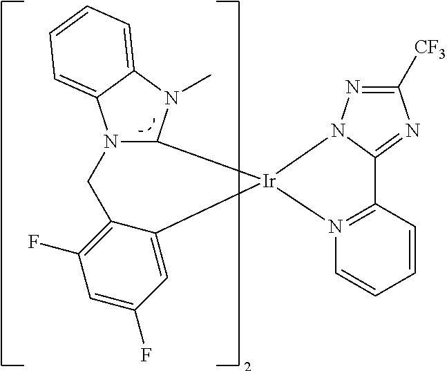
C00182
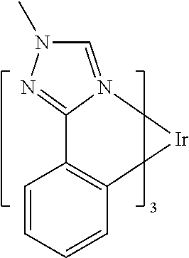
C00183
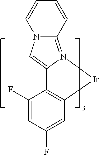
C00184
C00185
C00186
C00187
C00188
C00189
C00190
C00191
C00192
C00193
C00194
C00195
C00196
C00197
C00198
C00199
C00200
C00201
C00202
C00203
C00204
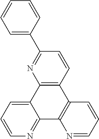
C00205
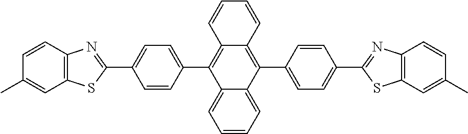
C00206
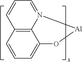
C00207
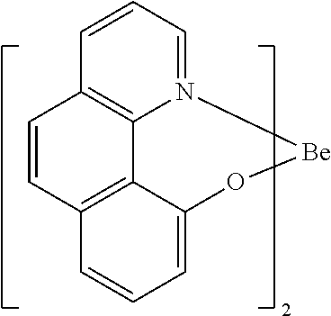
C00208
C00209
C00210

C00211
C00212
C00213
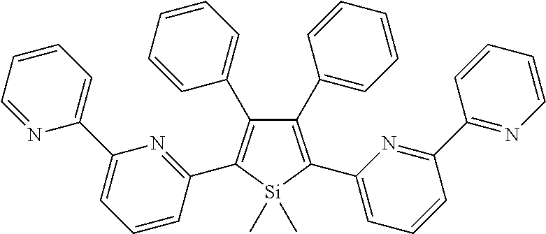
C00214
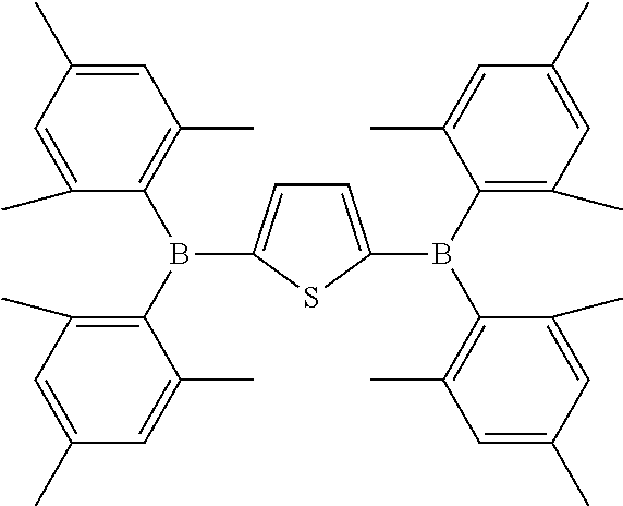
C00215
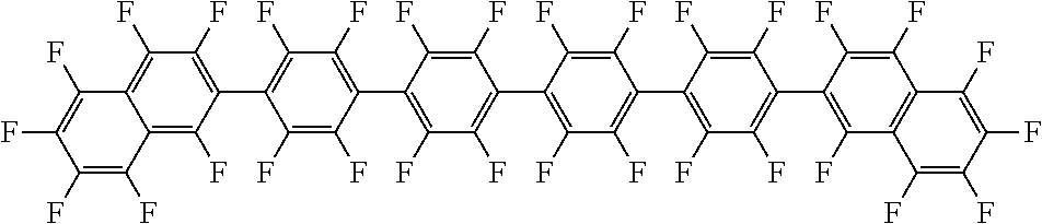
C00216
C00217

C00218
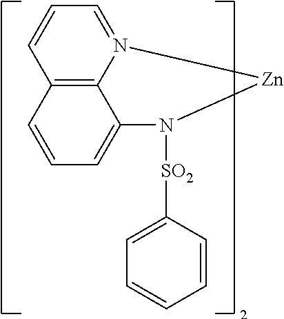
C00219
C00220
C00221
C00222
C00223

C00224
C00225

C00226

C00227
C00228
C00229

C00230

C00231

C00232
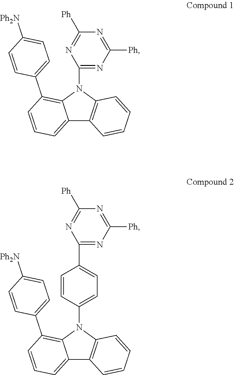
C00233
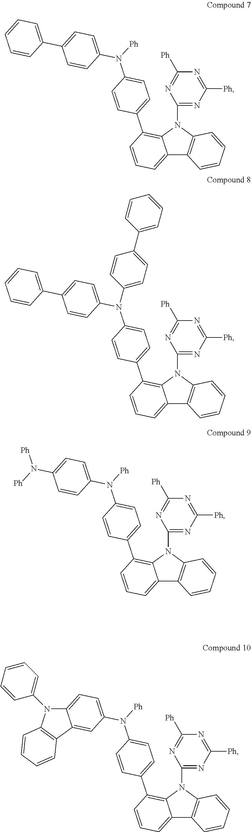
C00234

C00235
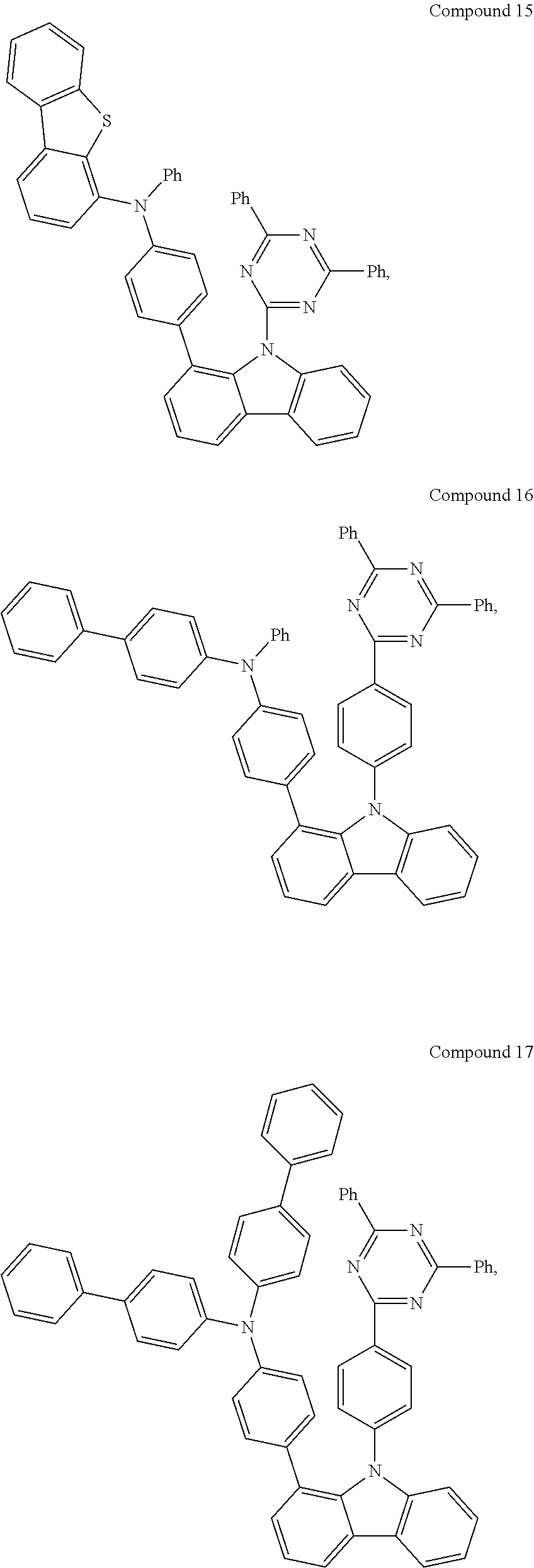
C00236
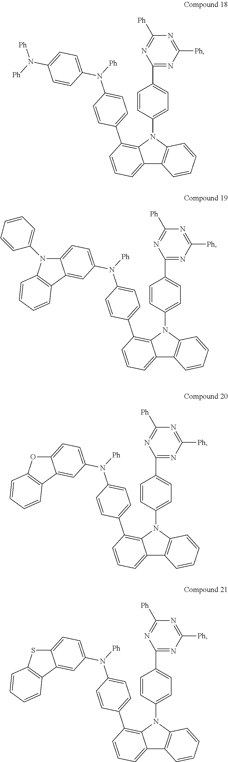
C00237
C00238

C00239

C00240
C00241

C00242

C00243
D00000
D00001
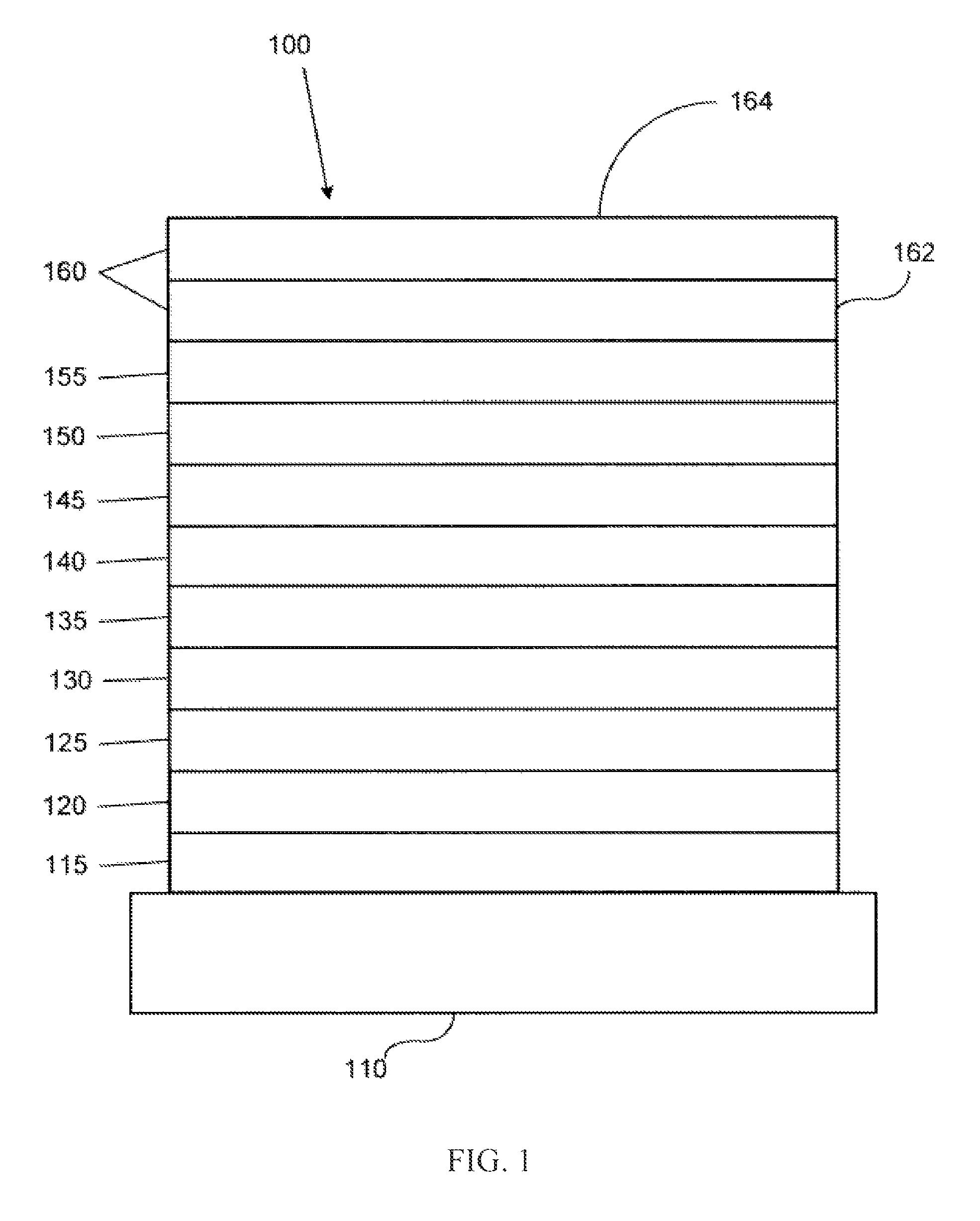
D00002
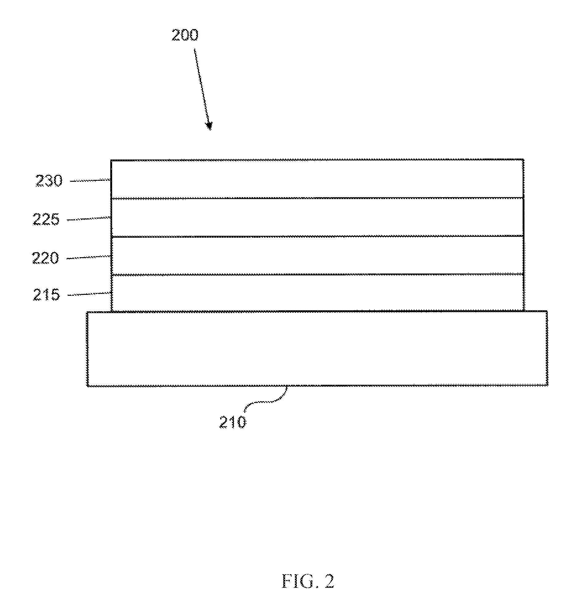
D00003
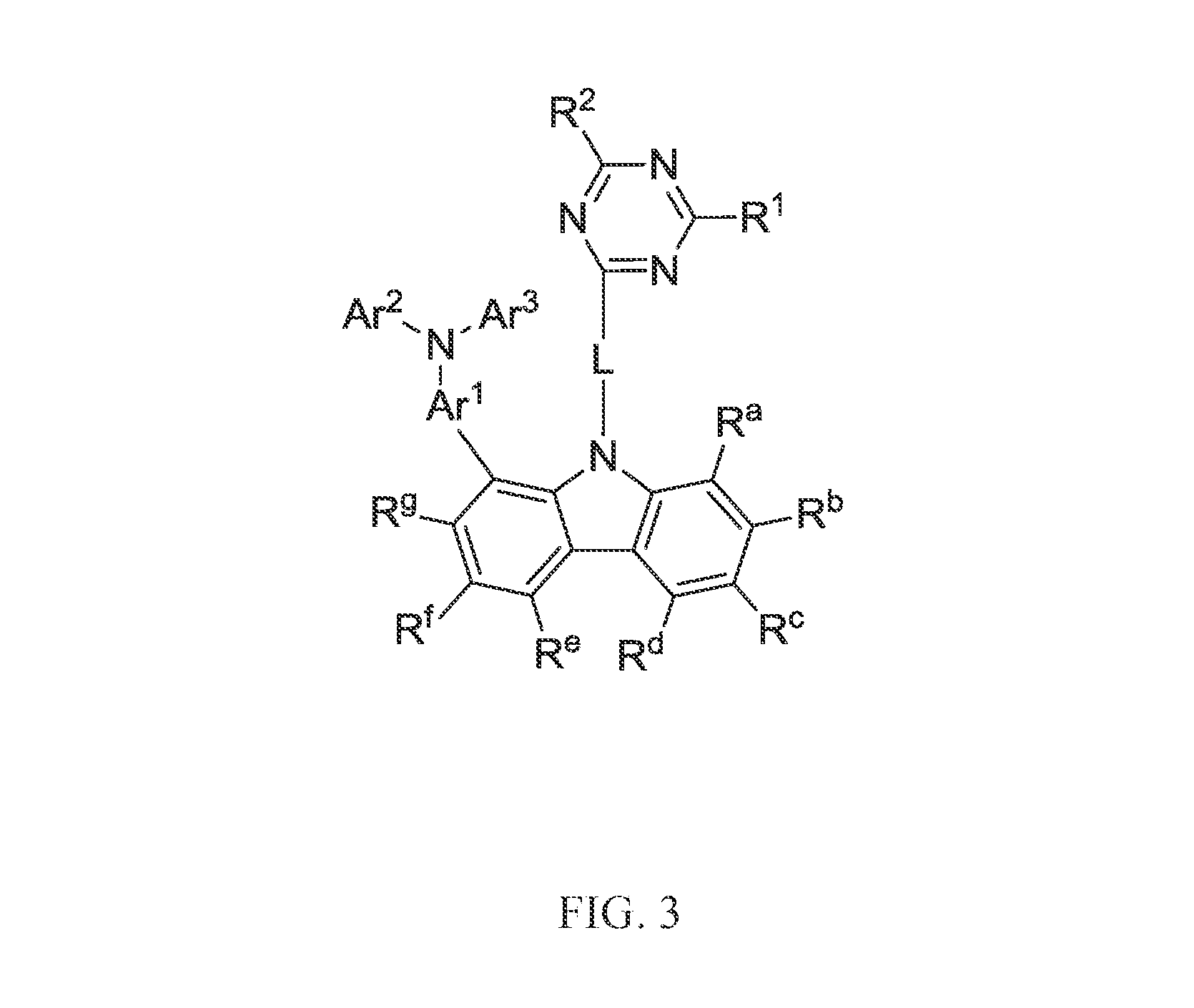
XML
uspto.report is an independent third-party trademark research tool that is not affiliated, endorsed, or sponsored by the United States Patent and Trademark Office (USPTO) or any other governmental organization. The information provided by uspto.report is based on publicly available data at the time of writing and is intended for informational purposes only.
While we strive to provide accurate and up-to-date information, we do not guarantee the accuracy, completeness, reliability, or suitability of the information displayed on this site. The use of this site is at your own risk. Any reliance you place on such information is therefore strictly at your own risk.
All official trademark data, including owner information, should be verified by visiting the official USPTO website at www.uspto.gov. This site is not intended to replace professional legal advice and should not be used as a substitute for consulting with a legal professional who is knowledgeable about trademark law.