Chemical sensor array having multiple sensors per well
Rothberg , et al. Oc
U.S. patent number 10,458,942 [Application Number 14/293,247] was granted by the patent office on 2019-10-29 for chemical sensor array having multiple sensors per well. This patent grant is currently assigned to LIFE TECHNOLOGIES CORPORATION. The grantee listed for this patent is LIFE TECHNOLOGIES CORPORATION. Invention is credited to James Bustillo, Keith G. Fife, Jordan Owens, Jonathan M. Rothberg.


View All Diagrams
| United States Patent | 10,458,942 |
| Rothberg , et al. | October 29, 2019 |
Chemical sensor array having multiple sensors per well
Abstract
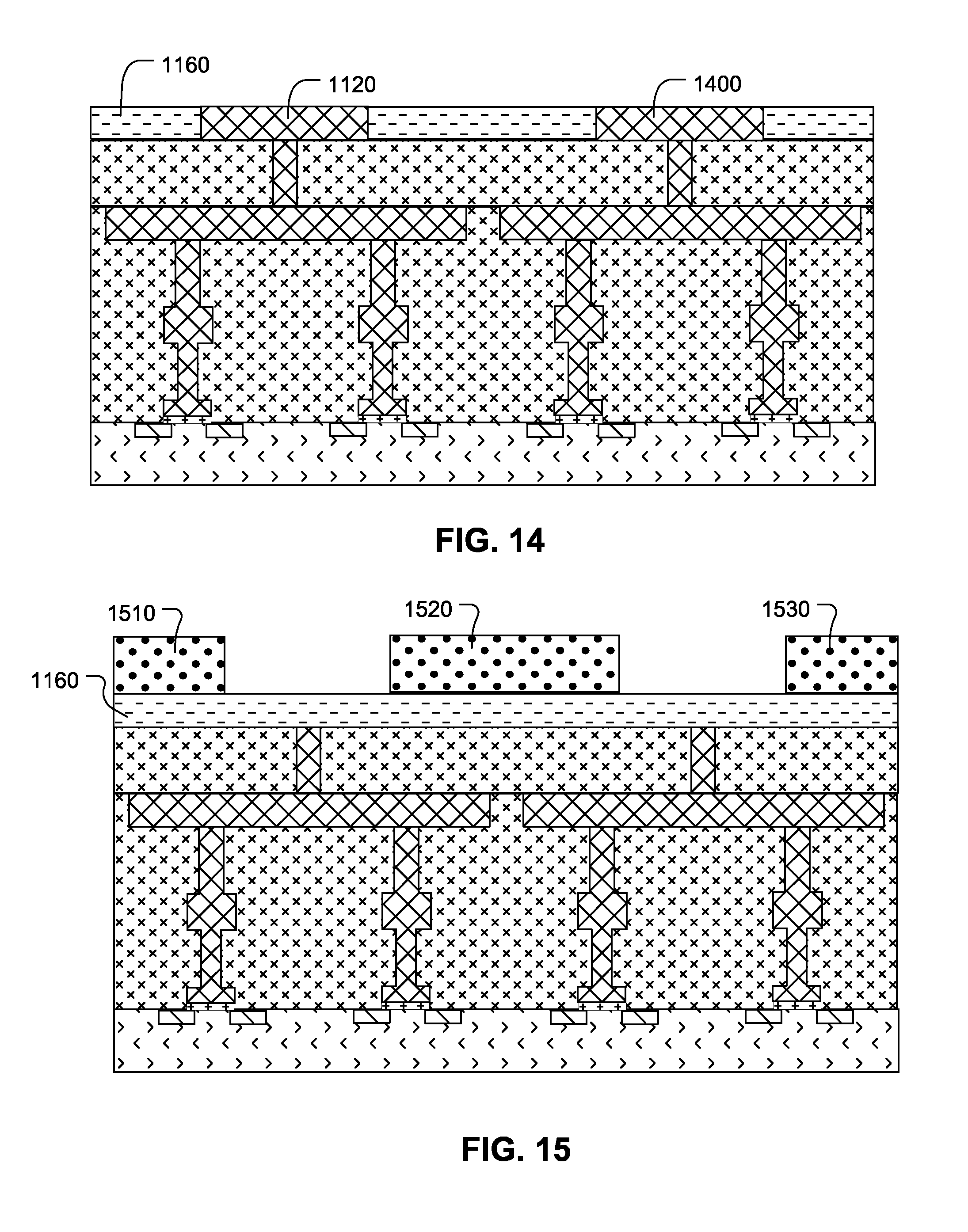
In one embodiment, a device is described. The device includes a material defining a reaction region. The device also includes a plurality of chemically-sensitive field effect transistors have a common floating gate in communication with the reaction region. The device also includes a circuit to obtain respective output signals from the chemically-sensitive field effect transistors indicating an analyte within the reaction region.
| Inventors: | Rothberg; Jonathan M. (Guilford, CT), Fife; Keith G. (Palo Alto, CA), Bustillo; James (Castro Valley, CA), Owens; Jordan (Austin, TX) | ||||||||||
|---|---|---|---|---|---|---|---|---|---|---|---|
| Applicant: |
|
||||||||||
| Assignee: | LIFE TECHNOLOGIES CORPORATION
(Carlsbad, CA) |
||||||||||
| Family ID: | 51023193 | ||||||||||
| Appl. No.: | 14/293,247 | ||||||||||
| Filed: | June 2, 2014 |
Prior Publication Data
| Document Identifier | Publication Date | |
|---|---|---|
| US 20140364320 A1 | Dec 11, 2014 | |
Related U.S. Patent Documents
| Application Number | Filing Date | Patent Number | Issue Date | ||
|---|---|---|---|---|---|
| 61833375 | Jun 10, 2013 | ||||
| Current U.S. Class: | 1/1 |
| Current CPC Class: | H01L 29/66825 (20130101); C12Q 1/6874 (20130101); G01N 27/414 (20130101); G01N 27/4145 (20130101) |
| Current International Class: | G01N 27/403 (20060101); G01N 27/414 (20060101); C12Q 1/6874 (20180101); H01L 29/66 (20060101) |
References Cited [Referenced By]
U.S. Patent Documents
| 4086642 | April 1978 | Yoshida et al. |
| 4411741 | October 1983 | Janata |
| 4437969 | March 1984 | Covington et al. |
| 4438354 | March 1984 | Haque et al. |
| 4444644 | April 1984 | Hiramoto |
| 4490678 | December 1984 | Kuisl et al. |
| 4641084 | February 1987 | Komatsu |
| 4660063 | April 1987 | Anthony |
| 4691167 | September 1987 | Vlekkert et al. |
| 4701253 | October 1987 | Litenberg et al. |
| 4722830 | February 1988 | Urie et al. |
| 4743954 | May 1988 | Brown |
| 4764797 | August 1988 | Shaw et al. |
| 4777019 | October 1988 | Dandekar |
| 4822566 | April 1989 | Newman |
| 4863849 | September 1989 | Melamede |
| 4864229 | September 1989 | Lauks et al. |
| 4874499 | October 1989 | Smith et al. |
| 4893088 | January 1990 | Myers et al. |
| 4927736 | May 1990 | Mueller et al. |
| 4971903 | November 1990 | Hyman |
| 5009766 | April 1991 | Lauks |
| 5038192 | August 1991 | Bonneau et al. |
| 5110441 | May 1992 | Kinlen et al. |
| 5113870 | May 1992 | Rossenfeld |
| 5126759 | June 1992 | Small et al. |
| 5138251 | August 1992 | Koshiishi et al. |
| 5140393 | August 1992 | Hijikihigawa et al. |
| 5142236 | August 1992 | Maloberti et al. |
| 5151587 | September 1992 | Machida et al. |
| 5151759 | September 1992 | Vinal |
| 5164319 | November 1992 | Hafeman et al. |
| 5202576 | April 1993 | Liu et al. |
| 5284566 | February 1994 | Cuomo et al. |
| 5317407 | May 1994 | Michon |
| 5319226 | June 1994 | Sohn et al. |
| 5407854 | April 1995 | Baxter et al. |
| 5436149 | July 1995 | Barnes |
| 5439839 | August 1995 | Jang |
| 5466348 | November 1995 | Holm-Kennedy |
| 5475337 | December 1995 | Tatsumi |
| 5490971 | February 1996 | Gifford et al. |
| 5554339 | September 1996 | Cozzette et al. |
| 5583462 | December 1996 | Grasshoff |
| 5587894 | December 1996 | Naruo |
| 5593838 | January 1997 | Zanzucchi et al. |
| 5600451 | February 1997 | Maki |
| 5627403 | May 1997 | Bacchetta et al. |
| 5631704 | May 1997 | Dickinson et al. |
| 5637469 | June 1997 | Wilding et al. |
| 5646558 | July 1997 | Jamshidi et al. |
| 5702964 | December 1997 | Lee |
| 5793230 | August 1998 | Chu et al. |
| 5846708 | December 1998 | Hollis et al. |
| 5894284 | April 1999 | Garrity et al. |
| 5907765 | May 1999 | Lescouzeres et al. |
| 5911873 | June 1999 | McCarron et al. |
| 5912560 | June 1999 | Pasternak |
| 5922591 | July 1999 | Anderson et al. |
| 5923421 | July 1999 | Rajic et al. |
| 5944970 | August 1999 | Rosenblatt |
| 5958703 | September 1999 | Dower et al. |
| 5965452 | October 1999 | Kovacs |
| 6002299 | December 1999 | Thomsen |
| 6021172 | February 2000 | Fossum et al. |
| 6107032 | August 2000 | Kilger et al. |
| 6191444 | February 2001 | Clampitt et al. |
| 6195585 | February 2001 | Karunasiri et al. |
| 6210891 | April 2001 | Nyren et al. |
| 6255678 | July 2001 | Sawada et al. |
| 6262568 | July 2001 | Komatsu et al. |
| 6274320 | August 2001 | Rothberg et al. |
| 6275061 | August 2001 | Tomita |
| 6280586 | August 2001 | Wolf et al. |
| 6294133 | September 2001 | Sawada et al. |
| 6327410 | December 2001 | Walt et al. |
| 6353324 | March 2002 | Uber, III et al. |
| 6355431 | March 2002 | Chee et al. |
| 6361671 | March 2002 | Mathies et al. |
| 6372291 | April 2002 | Hua et al. |
| 6376256 | April 2002 | Dunnington et al. |
| 6384684 | May 2002 | Redman-White |
| 6403957 | June 2002 | Fodor et al. |
| 6406848 | June 2002 | Bridgham et al. |
| 6413792 | July 2002 | Sauer et al. |
| 6429027 | August 2002 | Chee et al. |
| 6432360 | August 2002 | Church |
| 6433386 | August 2002 | Yun et al. |
| 6459398 | October 2002 | Gureshnik et al. |
| 6465178 | October 2002 | Chappa et al. |
| 6475728 | November 2002 | Martin et al. |
| 6482639 | November 2002 | Snow et al. |
| 6485944 | November 2002 | Church et al. |
| 6490220 | December 2002 | Merritt et al. |
| 6499499 | December 2002 | Dantsker et al. |
| 6511803 | January 2003 | Church et al. |
| 6518024 | February 2003 | Choong et al. |
| 6518146 | February 2003 | Singh et al. |
| 6535824 | March 2003 | Mansky et al. |
| 6537881 | March 2003 | Rangarajan et al. |
| 6538593 | March 2003 | Yang et al. |
| 6545620 | April 2003 | Groeneweg |
| 6571189 | May 2003 | Jensen et al. |
| 6602702 | August 2003 | McDevitt et al. |
| 6605428 | August 2003 | Kilger et al. |
| 6613513 | September 2003 | Parce et al. |
| 6618083 | September 2003 | Chen et al. |
| 6624637 | September 2003 | Pechstein |
| 6627154 | September 2003 | Goodman et al. |
| 6654505 | November 2003 | Bridgham et al. |
| 6657269 | December 2003 | Migliorato et al. |
| 6671341 | December 2003 | Kinget et al. |
| 6682899 | January 2004 | Bryan et al. |
| 6682936 | January 2004 | Kovacs |
| 6686638 | February 2004 | Fischer et al. |
| 6700814 | March 2004 | Nahas et al. |
| 6703660 | March 2004 | Yitzchaik et al. |
| 6716629 | April 2004 | Hess et al. |
| 6762022 | July 2004 | Makarov et al. |
| 6770472 | August 2004 | Manalis et al. |
| 6780591 | August 2004 | Williams et al. |
| 6795006 | September 2004 | Delight et al. |
| 6806052 | October 2004 | Bridgham et al. |
| 6828100 | December 2004 | Ronaghi |
| 6831994 | December 2004 | Bridgham et al. |
| 6841128 | January 2005 | Kambara et al. |
| 6859570 | February 2005 | Walt et al. |
| 6878255 | April 2005 | Wang et al. |
| 6888194 | May 2005 | Yoshino |
| 6898121 | May 2005 | Chien et al. |
| 6906524 | June 2005 | Chung et al. |
| 6919211 | July 2005 | Fodor et al. |
| 6926865 | August 2005 | Howard |
| 6927045 | August 2005 | Hadd et al. |
| 6929944 | August 2005 | Matson |
| 6939451 | September 2005 | Zhao et al. |
| 6953958 | October 2005 | Baxter et al. |
| 6958216 | October 2005 | Kelley et al. |
| 6969488 | November 2005 | Bridgham et al. |
| 6998274 | February 2006 | Chee et al. |
| 7008550 | March 2006 | Li et al. |
| 7019305 | March 2006 | Eversmann et al. |
| 7022288 | April 2006 | Boss |
| 7033754 | April 2006 | Chee et al. |
| 7037687 | May 2006 | Williams et al. |
| 7045097 | May 2006 | Kovacs |
| 7049645 | May 2006 | Sawada et al. |
| 7060431 | June 2006 | Chee et al. |
| 7067886 | June 2006 | Bonges et al. |
| 7084641 | August 2006 | Brederlow et al. |
| 7085502 | August 2006 | Shushakob et al. |
| 7087387 | August 2006 | Gerdes et al. |
| 7090975 | August 2006 | Shultz et al. |
| 7091059 | August 2006 | Rhodes |
| 7092757 | August 2006 | Larson et al. |
| 7097973 | August 2006 | Zenhausern |
| 7105300 | September 2006 | Parce et al. |
| 7106089 | September 2006 | Nakano et al. |
| 7129554 | October 2006 | Lieber et al. |
| 7169560 | January 2007 | Lapidus et al. |
| 7173445 | February 2007 | Fujii et al. |
| 7190026 | March 2007 | Lotfi et al. |
| 7192745 | March 2007 | Jaeger |
| 7193453 | March 2007 | Wei et al. |
| 7211390 | May 2007 | Rothberg et al. |
| 7220550 | May 2007 | Keen |
| 7223540 | May 2007 | Pourmand et al. |
| 7226734 | June 2007 | Chee et al. |
| 7229799 | June 2007 | Williams et al. |
| 7235389 | June 2007 | Lim et al. |
| 7238323 | July 2007 | Knapp et al. |
| 7239188 | July 2007 | Xu et al. |
| 7244559 | July 2007 | Rothberg et al. |
| 7244567 | July 2007 | Chen et al. |
| 7264929 | September 2007 | Rothberg et al. |
| 7264934 | September 2007 | Fuller |
| 7265929 | September 2007 | Umeda et al. |
| 7267751 | September 2007 | Gelbart et al. |
| 7276749 | October 2007 | Martin et al. |
| 7279588 | October 2007 | Hong et al. |
| 7282370 | October 2007 | Bridgham et al. |
| 7285384 | October 2007 | Fan et al. |
| 7291496 | November 2007 | Holm-Kennedy |
| 7297518 | November 2007 | Quake et al. |
| 7298475 | November 2007 | Gandhi et al. |
| 7303875 | December 2007 | Bock et al. |
| 7317216 | January 2008 | Holm-Kennedy |
| 7317484 | January 2008 | Dosluoglu et al. |
| 7323305 | January 2008 | Leamon et al. |
| 7335526 | February 2008 | Peters et al. |
| 7335762 | February 2008 | Rothberg et al. |
| 7359058 | April 2008 | Kranz et al. |
| 7361946 | April 2008 | Johnson et al. |
| 7363717 | April 2008 | Ekseth et al. |
| 7381936 | June 2008 | Tan et al. |
| 7394263 | July 2008 | Pechstein et al. |
| 7419636 | September 2008 | Aker et al. |
| 7425431 | September 2008 | Church et al. |
| 7455971 | November 2008 | Chee et al. |
| 7462452 | December 2008 | Williams et al. |
| 7462512 | December 2008 | Levon et al. |
| 7462709 | December 2008 | Jaeger |
| 7465512 | December 2008 | Wright et al. |
| 7466258 | December 2008 | Akopyan et al. |
| 7470352 | December 2008 | Eversmann et al. |
| 7476504 | January 2009 | Turner |
| 7482153 | January 2009 | Okada et al. |
| 7482677 | January 2009 | Lee et al. |
| 7499513 | March 2009 | Tetzlaff et al. |
| 7515124 | April 2009 | Yaguma et al. |
| 7534097 | May 2009 | Wong et al. |
| 7538827 | May 2009 | Chou |
| 7575865 | August 2009 | Leamon et al. |
| 7576037 | August 2009 | Engelhardt et al. |
| 7590211 | September 2009 | Burney |
| 7595883 | September 2009 | El Gamal et al. |
| 7605650 | October 2009 | Forbes |
| 7608810 | October 2009 | Yamada |
| 7609093 | October 2009 | Sarig et al. |
| 7609303 | October 2009 | Lee et al. |
| 7612369 | November 2009 | Stasiak |
| 7612817 | November 2009 | Tay |
| 7614135 | November 2009 | Santini, Jr. et al. |
| 7622294 | November 2009 | Walt et al. |
| 7645596 | January 2010 | Williams et al. |
| 7649358 | January 2010 | Toumazou et al. |
| 7667501 | February 2010 | Surendranath et al. |
| 7686929 | March 2010 | Toumazou et al. |
| 7695907 | April 2010 | Miyahara et al. |
| 7733401 | June 2010 | Takeda |
| 7772383 | August 2010 | Chakrabarti et al. |
| 7785785 | August 2010 | Pourmand et al. |
| 7785790 | August 2010 | Church et al. |
| 7794584 | September 2010 | Chodavarapu et al. |
| 7821806 | October 2010 | Horiuchi |
| 7824900 | November 2010 | Iwadate et al. |
| 7838226 | November 2010 | Kamahori et al. |
| 7842377 | November 2010 | Lanphere et al. |
| 7842457 | November 2010 | Berka et al. |
| 7859029 | December 2010 | Lee et al. |
| 7859291 | December 2010 | Kim |
| 7875440 | January 2011 | Williams et al. |
| 7884398 | February 2011 | Levon et al. |
| 7885490 | February 2011 | Heideman et al. |
| 7888013 | February 2011 | Miyahara et al. |
| 7888015 | February 2011 | Toumazou et al. |
| 7888708 | February 2011 | Yazawa et al. |
| 7890891 | February 2011 | Stuber et al. |
| 7898277 | March 2011 | Weir |
| 7923240 | April 2011 | Su |
| 7927797 | April 2011 | Nobile et al. |
| 7932034 | April 2011 | Esfandyarpour et al. |
| 7948015 | May 2011 | Rothberg et al. |
| 7955995 | June 2011 | Kakehata et al. |
| 7960776 | June 2011 | Kim et al. |
| 7972828 | July 2011 | Ward et al. |
| 7981362 | July 2011 | Glezer et al. |
| 8012690 | September 2011 | Berka et al. |
| 8017938 | September 2011 | Gomez et al. |
| 8035175 | October 2011 | Shim et al. |
| 8052863 | November 2011 | Suzuki et al. |
| 8067731 | November 2011 | Matyjaszczyk et al. |
| 8072188 | December 2011 | Yorinobu et al. |
| 8114591 | February 2012 | Toumazou et al. |
| 8124936 | February 2012 | Lagna |
| 8133698 | March 2012 | Silver et al. |
| 8138496 | March 2012 | Li et al. |
| 8154480 | April 2012 | Shishido et al. |
| 8199859 | June 2012 | Zerbe et al. |
| 8217433 | July 2012 | Fife |
| 8227877 | July 2012 | Lee et al. |
| 8231831 | July 2012 | Hartzell et al. |
| 8232813 | July 2012 | Burdett et al. |
| 8247849 | August 2012 | Fife et al. |
| 8248356 | August 2012 | Chen |
| 8262900 | September 2012 | Rothberg et al. |
| 8263336 | September 2012 | Rothberg et al. |
| 8264014 | September 2012 | Rothberg et al. |
| 8269261 | September 2012 | Rothberg et al. |
| 8277628 | October 2012 | Ronaghi et al. |
| 8293082 | October 2012 | Rothberg et al. |
| 8306757 | November 2012 | Rothberg et al. |
| 8313625 | November 2012 | Rothberg et al. |
| 8313639 | November 2012 | Rothberg et al. |
| 8317999 | November 2012 | Rothberg et al. |
| 8340914 | December 2012 | Gatewood et al. |
| 8343856 | January 2013 | Therrien et al. |
| 8349167 | January 2013 | Rothberg et al. |
| 8357547 | January 2013 | Lee et al. |
| 8361713 | January 2013 | Bridgham et al. |
| 8383896 | February 2013 | Kamahori et al. |
| 8415716 | April 2013 | Rothberg et al. |
| 8421437 | April 2013 | Levine |
| 8426898 | April 2013 | Rothberg et al. |
| 8426899 | April 2013 | Rothberg et al. |
| 8435395 | May 2013 | Rothberg et al. |
| 8441044 | May 2013 | Rothberg et al. |
| 8445194 | May 2013 | Drmanac et al. |
| 8445945 | May 2013 | Rothberg et al. |
| 8449824 | May 2013 | Sun |
| 8450781 | May 2013 | Rothberg et al. |
| 8470164 | June 2013 | Rothberg et al. |
| 8487790 | July 2013 | Fife et al. |
| 8492800 | July 2013 | Rothberg et al. |
| 8496802 | July 2013 | Rothberg et al. |
| 8502278 | August 2013 | Rothberg et al. |
| 8519448 | August 2013 | Rothberg et al. |
| 8524057 | September 2013 | Rothberg et al. |
| 8530941 | September 2013 | Rothberg et al. |
| 8535513 | September 2013 | Rothberg et al. |
| 8552771 | October 2013 | Jordan et al. |
| 8558288 | October 2013 | Rothberg et al. |
| 8575664 | November 2013 | Rothberg et al. |
| 8592154 | November 2013 | Rearick et al. |
| 8653567 | February 2014 | Fife |
| 8658017 | February 2014 | Rothberg et al. |
| 8673627 | March 2014 | Nobile et al. |
| 8685230 | April 2014 | Rothberg et al. |
| 8685298 | April 2014 | Rothberg et al. |
| 8728844 | May 2014 | Liu et al. |
| 8731847 | May 2014 | Johnson et al. |
| 8742469 | June 2014 | Milgrew |
| 8742472 | June 2014 | Rothberg et al. |
| 8747748 | June 2014 | Li et al. |
| 8748947 | June 2014 | Milgrew |
| 8764969 | July 2014 | Rothberg et al. |
| 8766327 | July 2014 | Milgrew |
| 8766328 | July 2014 | Rothberg et al. |
| 8776573 | July 2014 | Rearick et al. |
| 8786331 | July 2014 | Jordan et al. |
| 8796036 | August 2014 | Fife et al. |
| 8821798 | September 2014 | Bustillo et al. |
| 8823380 | September 2014 | Levin et al. |
| 8841217 | September 2014 | Fife et al. |
| 8847637 | September 2014 | Guyton |
| 8912005 | December 2014 | Fife et al. |
| 8945912 | February 2015 | Bashir et al. |
| 8962366 | February 2015 | Putnam et al. |
| 8963216 | February 2015 | Fife et al. |
| 8983783 | March 2015 | Johnson et al. |
| 9023674 | May 2015 | Shen et al. |
| 9164070 | October 2015 | Fife |
| 9201041 | December 2015 | Dalton et al. |
| 9270264 | February 2016 | Jordan et al. |
| 9389199 | July 2016 | Cheng et al. |
| 9618475 | April 2017 | Rothberg et al. |
| 9671363 | June 2017 | Fife et al. |
| 2001/0024790 | September 2001 | Kambara et al. |
| 2002/0001801 | January 2002 | Fan et al. |
| 2002/0012930 | January 2002 | Rothberg et al. |
| 2002/0012933 | January 2002 | Rothberg et al. |
| 2002/0012937 | January 2002 | Tender et al. |
| 2002/0029971 | March 2002 | Kovacs |
| 2002/0042059 | April 2002 | Makarov et al. |
| 2002/0042388 | April 2002 | Cooper et al. |
| 2002/0050611 | May 2002 | Yitzchaik et al. |
| 2002/0081714 | June 2002 | Jain et al. |
| 2002/0085136 | July 2002 | Moon et al. |
| 2002/0086318 | July 2002 | Manalis et al. |
| 2002/0094533 | July 2002 | Hess et al. |
| 2002/0117694 | August 2002 | Migliorato |
| 2002/0150909 | October 2002 | Stuelpnagel et al. |
| 2002/0168678 | November 2002 | Williams et al. |
| 2002/0172963 | November 2002 | Kelley et al. |
| 2003/0020334 | January 2003 | Nozu |
| 2003/0032052 | February 2003 | Hadd et al. |
| 2003/0044799 | March 2003 | Matson |
| 2003/0044833 | March 2003 | Benchikh et al. |
| 2003/0054396 | March 2003 | Weiner |
| 2003/0064366 | April 2003 | Hardin et al. |
| 2003/0068629 | April 2003 | Rothberg et al. |
| 2003/0100102 | May 2003 | Rothberg et al. |
| 2003/0102510 | June 2003 | Lim et al. |
| 2003/0108867 | June 2003 | Chee et al. |
| 2003/0119020 | June 2003 | Stevens et al. |
| 2003/0124572 | July 2003 | Umek et al. |
| 2003/0124599 | July 2003 | Chen et al. |
| 2003/0141928 | July 2003 | Lee et al. |
| 2003/0141929 | July 2003 | Casper et al. |
| 2003/0148301 | August 2003 | Aono et al. |
| 2003/0148344 | August 2003 | Rothberg et al. |
| 2003/0152929 | August 2003 | Howard |
| 2003/0152994 | August 2003 | Woudenberg et al. |
| 2003/0155942 | August 2003 | Thewes et al. |
| 2003/0175990 | September 2003 | Hayenga et al. |
| 2003/0186262 | October 2003 | Cailloux et al. |
| 2003/0211502 | November 2003 | Sauer et al. |
| 2003/0215791 | November 2003 | Garini et al. |
| 2003/0215857 | November 2003 | Kilger et al. |
| 2003/0224419 | December 2003 | Corcoran et al. |
| 2003/0227296 | December 2003 | Lee |
| 2003/0231531 | December 2003 | Baxter et al. |
| 2004/0002470 | January 2004 | Keith et al. |
| 2004/0012998 | January 2004 | Chien et al. |
| 2004/0023253 | February 2004 | Kunwar et al. |
| 2004/0038420 | February 2004 | Gelbart et al. |
| 2004/0079636 | April 2004 | Hsia et al. |
| 2004/0106211 | June 2004 | Kauer et al. |
| 2004/0121354 | June 2004 | Yazawa et al. |
| 2004/0130377 | July 2004 | Takeda et al. |
| 2004/0134798 | July 2004 | Toumazou et al. |
| 2004/0136866 | July 2004 | Pontis et al. |
| 2004/0146849 | July 2004 | Huang et al. |
| 2004/0185484 | September 2004 | Costa et al. |
| 2004/0185591 | September 2004 | Hsiung et al. |
| 2004/0197803 | October 2004 | Yaku et al. |
| 2004/0235216 | November 2004 | Rhodes |
| 2004/0248161 | December 2004 | Rothberg et al. |
| 2005/0006234 | January 2005 | Hassibi |
| 2005/0009022 | January 2005 | Weiner et al. |
| 2005/0017190 | January 2005 | Eversmann |
| 2005/0031490 | February 2005 | Gumbrecht et al. |
| 2005/0032075 | February 2005 | Yaku et al. |
| 2005/0032076 | February 2005 | Williams et al. |
| 2005/0058990 | March 2005 | Guia et al. |
| 2005/0062093 | March 2005 | Sawada et al. |
| 2005/0079510 | April 2005 | Berka et al. |
| 2005/0093072 | May 2005 | Bonges et al. |
| 2005/0093645 | May 2005 | Watanabe et al. |
| 2005/0106587 | May 2005 | Klapproth |
| 2005/0142033 | June 2005 | Glezer et al. |
| 2005/0151181 | July 2005 | Beintner et al. |
| 2005/0156207 | July 2005 | Yazawa et al. |
| 2005/0156584 | July 2005 | Feng |
| 2005/0181440 | August 2005 | Chee et al. |
| 2005/0189960 | September 2005 | Tajima |
| 2005/0191698 | September 2005 | Chee et al. |
| 2005/0202582 | September 2005 | Eversmann et al. |
| 2005/0206548 | September 2005 | Muramatsu |
| 2005/0212016 | September 2005 | Brunner et al. |
| 2005/0221473 | October 2005 | Dubin et al. |
| 2005/0230245 | October 2005 | Morgenshtein et al. |
| 2005/0230271 | October 2005 | Levon et al. |
| 2005/0233318 | October 2005 | Chee et al. |
| 2005/0239132 | October 2005 | Klapproth |
| 2005/0266456 | December 2005 | Williams et al. |
| 2005/0282224 | December 2005 | Fouillet et al. |
| 2005/0285155 | December 2005 | Johnson et al. |
| 2006/0000772 | January 2006 | Sano et al. |
| 2006/0024711 | February 2006 | Lapidus et al. |
| 2006/0035400 | February 2006 | Wu et al. |
| 2006/0038601 | February 2006 | Giguere |
| 2006/0040297 | February 2006 | Leamon et al. |
| 2006/0057025 | March 2006 | Eversmann et al. |
| 2006/0057604 | March 2006 | Chen et al. |
| 2006/0073513 | April 2006 | Chee et al. |
| 2006/0134633 | June 2006 | Chen et al. |
| 2006/0141474 | June 2006 | Miyahara et al. |
| 2006/0154399 | July 2006 | Sauer et al. |
| 2006/0166203 | July 2006 | Tooke et al. |
| 2006/0182664 | August 2006 | Peck et al. |
| 2006/0197118 | September 2006 | Migliorato et al. |
| 2006/0199193 | September 2006 | Koo et al. |
| 2006/0199493 | September 2006 | Hartmann et al. |
| 2006/0205061 | September 2006 | Roukes |
| 2006/0216812 | September 2006 | Okada et al. |
| 2006/0219558 | October 2006 | Hafeman et al. |
| 2006/0228721 | October 2006 | Leamon et al. |
| 2006/0246497 | November 2006 | Huang et al. |
| 2006/0266946 | November 2006 | Defrise et al. |
| 2006/0269927 | November 2006 | Lieber |
| 2006/0289726 | December 2006 | Paulus et al. |
| 2007/0031291 | February 2007 | Piech et al. |
| 2007/0059741 | March 2007 | Kamahori et al. |
| 2007/0069291 | March 2007 | Stuber et al. |
| 2007/0087401 | April 2007 | Neilson et al. |
| 2007/0092872 | April 2007 | Rothberg et al. |
| 2007/0095663 | May 2007 | Chou et al. |
| 2007/0096164 | May 2007 | Peters et al. |
| 2007/0099173 | May 2007 | Spira et al. |
| 2007/0099208 | May 2007 | Drmanac et al. |
| 2007/0117099 | May 2007 | Engelhardt et al. |
| 2007/0138132 | June 2007 | Barth |
| 2007/0172865 | July 2007 | Hardin et al. |
| 2007/0212681 | September 2007 | Shapiro et al. |
| 2007/0217963 | September 2007 | Elizarov et al. |
| 2007/0231824 | October 2007 | Chee et al. |
| 2007/0233477 | October 2007 | Halowani et al. |
| 2007/0247170 | October 2007 | Barbaro et al. |
| 2007/0250274 | October 2007 | Volkov et al. |
| 2007/0252176 | November 2007 | Shim et al. |
| 2007/0262363 | November 2007 | Tao et al. |
| 2007/0278488 | December 2007 | Hirabayashi et al. |
| 2008/0003142 | January 2008 | Link et al. |
| 2008/0012007 | January 2008 | Li et al. |
| 2008/0014589 | January 2008 | Link et al. |
| 2008/0035494 | February 2008 | Gomez et al. |
| 2008/0047836 | February 2008 | Strand et al. |
| 2008/0063566 | March 2008 | Matsumoto et al. |
| 2008/0085219 | April 2008 | Beebe et al. |
| 2008/0094074 | April 2008 | Kim et al. |
| 2008/0096216 | April 2008 | Quake et al. |
| 2008/0111161 | May 2008 | Sorge et al. |
| 2008/0115361 | May 2008 | Santini et al. |
| 2008/0121946 | May 2008 | Youn et al. |
| 2008/0132693 | June 2008 | Berka et al. |
| 2008/0136933 | June 2008 | Dosluoglu et al. |
| 2008/0164917 | July 2008 | Floyd et al. |
| 2008/0176271 | July 2008 | Silver et al. |
| 2008/0178692 | July 2008 | Jung et al. |
| 2008/0185616 | August 2008 | Johnson et al. |
| 2008/0197022 | August 2008 | Suzuki et al. |
| 2008/0204048 | August 2008 | Stasiak et al. |
| 2008/0205559 | August 2008 | Iida |
| 2008/0210931 | September 2008 | Truong et al. |
| 2008/0230386 | September 2008 | Srinivasan et al. |
| 2008/0286762 | November 2008 | Miyahara et al. |
| 2009/0026082 | January 2009 | Rothberg et al. |
| 2009/0030117 | January 2009 | Lanphere et al. |
| 2009/0033370 | February 2009 | Sarig et al. |
| 2009/0048124 | February 2009 | Leamon et al. |
| 2009/0062132 | March 2009 | Bortner |
| 2009/0075383 | March 2009 | El Gamal et al. |
| 2009/0079414 | March 2009 | Levon et al. |
| 2009/0120905 | May 2009 | Kohl et al. |
| 2009/0121258 | May 2009 | Kumar |
| 2009/0127589 | May 2009 | Rothberg et al. |
| 2009/0127689 | May 2009 | Ye et al. |
| 2009/0140763 | June 2009 | Kim |
| 2009/0149607 | June 2009 | Karim et al. |
| 2009/0156425 | June 2009 | Walt et al. |
| 2009/0170728 | July 2009 | Walt et al. |
| 2009/0194416 | August 2009 | Hsiung et al. |
| 2009/0201032 | August 2009 | Burdett et al. |
| 2009/0273386 | November 2009 | Korobeynikov et al. |
| 2009/0299138 | December 2009 | Mitsuhashi |
| 2010/0007326 | January 2010 | Nakazato |
| 2010/0026814 | February 2010 | Shimoda |
| 2010/0039146 | February 2010 | Park et al. |
| 2010/0052765 | March 2010 | Makino |
| 2010/0105373 | April 2010 | Kanade |
| 2010/0133547 | June 2010 | Kunze et al. |
| 2010/0137143 | June 2010 | Rothberg et al. |
| 2010/0156454 | June 2010 | Weir |
| 2010/0176463 | July 2010 | Koizumi et al. |
| 2010/0188073 | July 2010 | Rothberg et al. |
| 2010/0197507 | August 2010 | Rothberg et al. |
| 2010/0244106 | September 2010 | Parker et al. |
| 2010/0273166 | October 2010 | Garcia |
| 2010/0282617 | November 2010 | Rothberg et al. |
| 2010/0300895 | December 2010 | Nobile et al. |
| 2010/0301398 | December 2010 | Rothberg et al. |
| 2011/0037121 | February 2011 | Lee et al. |
| 2011/0062972 | March 2011 | Je et al. |
| 2011/0114827 | May 2011 | Yamaoka et al. |
| 2011/0165557 | July 2011 | Ah et al. |
| 2011/0169056 | July 2011 | Wey et al. |
| 2011/0181253 | July 2011 | Isham et al. |
| 2011/0217697 | September 2011 | Rothberg et al. |
| 2011/0230375 | September 2011 | Rothberg et al. |
| 2011/0236263 | September 2011 | Sawada et al. |
| 2011/0247933 | October 2011 | Rothberg et al. |
| 2011/0248320 | October 2011 | Rothberg et al. |
| 2011/0262903 | October 2011 | Davidson et al. |
| 2011/0263463 | October 2011 | Rothberg et al. |
| 2011/0275522 | November 2011 | Rothberg et al. |
| 2011/0281737 | November 2011 | Rothberg et al. |
| 2011/0281741 | November 2011 | Rothberg et al. |
| 2011/0287945 | November 2011 | Rothberg et al. |
| 2011/0299337 | December 2011 | Parris et al. |
| 2012/0000274 | January 2012 | Fife |
| 2012/0001056 | January 2012 | Fife et al. |
| 2012/0001235 | January 2012 | Fife |
| 2012/0001236 | January 2012 | Fife et al. |
| 2012/0001237 | January 2012 | Fife et al. |
| 2012/0001615 | January 2012 | Levine et al. |
| 2012/0001646 | January 2012 | Bolander et al. |
| 2012/0001779 | January 2012 | Fife et al. |
| 2012/0012900 | January 2012 | Lee et al. |
| 2012/0013392 | January 2012 | Rothberg et al. |
| 2012/0022795 | January 2012 | Johnson et al. |
| 2012/0034607 | February 2012 | Rothberg et al. |
| 2012/0037961 | February 2012 | Rothberg et al. |
| 2012/0040844 | February 2012 | Rothberg et al. |
| 2012/0045368 | February 2012 | Hinz et al. |
| 2012/0045844 | February 2012 | Rothberg et al. |
| 2012/0055811 | March 2012 | Rothberg et al. |
| 2012/0055813 | March 2012 | Rothberg et al. |
| 2012/0056248 | March 2012 | Fife et al. |
| 2012/0060587 | March 2012 | Babcock et al. |
| 2012/0129703 | May 2012 | Rothberg et al. |
| 2012/0129728 | May 2012 | Rothberg et al. |
| 2012/0129732 | May 2012 | Rothberg et al. |
| 2012/0135870 | May 2012 | Rothberg et al. |
| 2012/0143531 | June 2012 | Davey et al. |
| 2012/0154018 | June 2012 | Sugiura |
| 2012/0161207 | June 2012 | Homyk et al. |
| 2012/0173159 | July 2012 | Davey et al. |
| 2012/0228136 | September 2012 | Levine |
| 2012/0247977 | October 2012 | Rothberg et al. |
| 2012/0249192 | October 2012 | Matsushita et al. |
| 2012/0261274 | October 2012 | Rearick et al. |
| 2012/0279859 | November 2012 | Rothberg et al. |
| 2012/0280285 | November 2012 | Rothberg et al. |
| 2012/0280286 | November 2012 | Rothberg et al. |
| 2012/0283146 | November 2012 | Rothberg et al. |
| 2012/0286332 | November 2012 | Rothberg et al. |
| 2012/0286333 | November 2012 | Rothberg et al. |
| 2012/0286771 | November 2012 | Rothberg et al. |
| 2012/0288853 | November 2012 | Rothberg et al. |
| 2012/0288976 | November 2012 | Rothberg et al. |
| 2012/0289413 | November 2012 | Rothberg et al. |
| 2012/0293158 | November 2012 | Rothberg et al. |
| 2012/0295795 | November 2012 | Rothberg et al. |
| 2012/0322054 | December 2012 | Rothberg et al. |
| 2012/0326213 | December 2012 | Bustillo et al. |
| 2012/0326767 | December 2012 | Milgrew |
| 2012/0329043 | December 2012 | Milgrew |
| 2012/0329044 | December 2012 | Milgrew |
| 2012/0329192 | December 2012 | Bustillo et al. |
| 2013/0001653 | January 2013 | Milgrew |
| 2013/0004949 | January 2013 | Rearick et al. |
| 2013/0009214 | January 2013 | Bustillo et al. |
| 2013/0015505 | January 2013 | Rothberg et al. |
| 2013/0015506 | January 2013 | Rothberg et al. |
| 2013/0017959 | January 2013 | Rothberg et al. |
| 2013/0027594 | January 2013 | Krymski |
| 2013/0056353 | March 2013 | Nemirovsky |
| 2013/0105868 | May 2013 | Kalnitsky et al. |
| 2013/0135018 | May 2013 | Kuo et al. |
| 2013/0189790 | July 2013 | Li et al. |
| 2013/0210128 | August 2013 | Rothberg et al. |
| 2013/0210182 | August 2013 | Rothberg et al. |
| 2013/0210641 | August 2013 | Rothberg et al. |
| 2013/0217004 | August 2013 | Rothberg et al. |
| 2013/0217587 | August 2013 | Rothberg et al. |
| 2013/0281307 | October 2013 | Li et al. |
| 2013/0324421 | December 2013 | Rothberg et al. |
| 2013/0341734 | December 2013 | Merz |
| 2014/0075237 | March 2014 | Ware |
| 2014/0080717 | March 2014 | Li et al. |
| 2014/0148345 | May 2014 | Li et al. |
| 2014/0234981 | August 2014 | Zarkesh-Ha et al. |
| 2014/0235452 | August 2014 | Rothberg et al. |
| 2014/0235463 | August 2014 | Rothberg et al. |
| 2014/0308752 | October 2014 | Chang et al. |
| 2014/0367748 | December 2014 | Dalton et al. |
| 2015/0097214 | April 2015 | Chen et al. |
| 2016/0178568 | June 2016 | Cheng et al. |
| 2017/0038334 | February 2017 | Barbee et al. |
| 2017/0059514 | March 2017 | Hoffman |
| 2017/0102356 | April 2017 | Lin et al. |
| 1582334 | Feb 2005 | CN | |||
| 1585896 | Feb 2005 | CN | |||
| 1703623 | Nov 2005 | CN | |||
| 1826525 | Aug 2006 | CN | |||
| 101669026 | Mar 2010 | CN | |||
| 101676714 | Mar 2010 | CN | |||
| 102203282 | Sep 2011 | CN | |||
| 102301228 | Dec 2011 | CN | |||
| 102484267 | May 2012 | CN | |||
| 4430811 | Sep 1995 | DE | |||
| 19512117 | Oct 1996 | DE | |||
| 102004044299 | Mar 2006 | DE | |||
| 102008012899 | Sep 2009 | DE | |||
| 1975246 | Mar 1984 | EP | |||
| 0223618 | May 1987 | EP | |||
| 1243925 | Sep 2002 | EP | |||
| 1371974 | Dec 2003 | EP | |||
| 1432818 | Jun 2004 | EP | |||
| 1542009 | Jun 2005 | EP | |||
| 1557884 | Jul 2005 | EP | |||
| 1669749 | Jun 2006 | EP | |||
| 1870703 | Dec 2007 | EP | |||
| 2307577 | Apr 2011 | EP | |||
| 2457851 | Sep 2009 | GB | |||
| 2461127 | Jul 2010 | GB | |||
| 58070155 | Apr 1983 | JP | |||
| 62-237349 | Oct 1987 | JP | |||
| 02-250331 | Oct 1990 | JP | |||
| 02-310931 | Dec 1990 | JP | |||
| H03122558 | May 1991 | JP | |||
| H05-080115 | Apr 1993 | JP | |||
| H10-078827 | Mar 1998 | JP | |||
| 2000055874 | Feb 2000 | JP | |||
| 2002-221510 | Aug 2002 | JP | |||
| 2002/272463 | Sep 2002 | JP | |||
| 2002272463 | Sep 2002 | JP | |||
| 2003-279532 | Oct 2003 | JP | |||
| 2003-322633 | Nov 2003 | JP | |||
| 2004-500033 | Jan 2004 | JP | |||
| 2005218310 | Aug 2004 | JP | |||
| 2004-271384 | Sep 2004 | JP | |||
| 2004-343441 | Dec 2004 | JP | |||
| 2005077210 | Mar 2005 | JP | |||
| 2005-515475 | May 2005 | JP | |||
| 2005518541 | Jun 2005 | JP | |||
| 2005-207797 | Aug 2005 | JP | |||
| 2006138846 | Jun 2006 | JP | |||
| 2006-284225 | Oct 2006 | JP | |||
| 2007-512810 | May 2007 | JP | |||
| 2008-215974 | Sep 2008 | JP | |||
| 2010513869 | Apr 2010 | JP | |||
| 2011525810 | Sep 2011 | JP | |||
| 2012-506557 | Mar 2012 | JP | |||
| 2015-506557 | Mar 2012 | JP | |||
| 100442838 | Jul 2004 | KR | |||
| 100455283 | Oct 2004 | KR | |||
| 200946904 | Nov 2009 | TW | |||
| WO1989009283 | Oct 1989 | WO | |||
| 1990/005910 | May 1990 | WO | |||
| WO1998013523 | Apr 1998 | WO | |||
| WO1998046797 | Oct 1998 | WO | |||
| WO2001020039 | Mar 2001 | WO | |||
| 2001/42498 | Jun 2001 | WO | |||
| 2001/047804 | Jul 2001 | WO | |||
| WO2001081896 | Nov 2001 | WO | |||
| WO2002077287 | Oct 2002 | WO | |||
| WO2002086162 | Oct 2002 | WO | |||
| WO2003073088 | Sep 2003 | WO | |||
| 2004/017068 | Feb 2004 | WO | |||
| WO2004040291 | May 2004 | WO | |||
| WO2004048962 | Jun 2004 | WO | |||
| WO-2004081234 | Sep 2004 | WO | |||
| WO2005015156 | Feb 2005 | WO | |||
| 2005/022142 | Mar 2005 | WO | |||
| WO2005043160 | May 2005 | WO | |||
| WO2005047878 | May 2005 | WO | |||
| WO2005054431 | Jun 2005 | WO | |||
| WO2005062049 | Jul 2005 | WO | |||
| WO2005084367 | Sep 2005 | WO | |||
| WO2005090961 | Sep 2005 | WO | |||
| WO2006005967 | Jan 2006 | WO | |||
| WO2006022370 | Mar 2006 | WO | |||
| 2006/056226 | Jun 2006 | WO | |||
| WO2007002204 | Jan 2007 | WO | |||
| WO2007086935 | Aug 2007 | WO | |||
| WO2008007716 | Jan 2008 | WO | |||
| WO2008058282 | May 2008 | WO | |||
| 2008076406 | Jun 2008 | WO | |||
| WO2008076406 | Jun 2008 | WO | |||
| WO2008107014 | Sep 2008 | WO | |||
| 2009/014155 | Jan 2009 | WO | |||
| WO2009012112 | Jan 2009 | WO | |||
| WO2009041917 | Apr 2009 | WO | |||
| WO2009074926 | Jun 2009 | WO | |||
| WO2009081890 | Jul 2009 | WO | |||
| WO2009158006 | Dec 2009 | WO | |||
| WO2010008480 | Jan 2010 | WO | |||
| WO2010047804 | Apr 2010 | WO | |||
| 2010/138186 | Dec 2010 | WO | |||
| 2010/138188 | Dec 2010 | WO | |||
| WO2010138182 | Dec 2010 | WO | |||
| WO2012003359 | Jan 2012 | WO | |||
| WO2012003363 | Jan 2012 | WO | |||
| WO2012003368 | Jan 2012 | WO | |||
| WO2012003380 | Jan 2012 | WO | |||
| WO2012006222 | Jan 2012 | WO | |||
| 2012/046137 | Apr 2012 | WO | |||
| WO2012152308 | Nov 2012 | WO | |||
Other References
|
Ahmadian, A. et al., "Single-nucleotide polymorphism analysis by pyrosequencing", Anal Biochem. vol. 280, 2000, pp. 103-110. cited by applicant . Dorf, Richard C. , "The Electrical Engineering Handbook", University of California, Davis, CRC Press, 2 edition, Chapter 3--Linear Circuit Analysis, Jun. 25, 2004, pp. 3-1 to 3-66. cited by applicant . EP13177590.0, "European Examination Notification", dated Sep. 8, 2014, 9 pages. cited by applicant . Gardner, J.W. et al., "Enhancing electronic nose performance by sensor selection using a new integer-based genetic algorithm approach", Science Direct, Sensors and Actuators B, vol. 106, 2005, pp. 114-121. cited by applicant . Hijikata, M. et al., "Identification of a Single Nucleotide Polymorphism in the MXA Gene Promoter (T/T at nt-88) Correlated with the Response of Hepatitis C Patients to Interferon", Intervirology, vol. 43, 2000, pp. 124-127. cited by applicant . Li, et al., "Sequence-Specific Label-Free DNA Sensors Based on Silico Nanowires", Nano Letters,, vol. 4(2), 2004, pp. 245-247. cited by applicant . Lin, B.J. et al., "Practicing the Novolac deep-UV portable conformable masking technique", Journal of Vacuum Science and Technology, Vo. 19, No. 4, 1981, 1313-1319. cited by applicant . Naidu, M. S., et al., "Introduction to Electrical Engineering", Chapter 1--Fundamental Concepts of Electricity, McGraw Hill Education (India) Private Limited, 1995, pp. 1-10. cited by applicant . Neaman, Donald A. , "Electronic Circuit Analysis and Design", McGraw Hill Higher Education, 2nd Edition, Chapter 6--Basic FET Amplifiers, (reference will be uploaded in 2 parts due to size) part 1 of 2, Dec. 1, 2000, pp. 313-345. cited by applicant . Neaman, Donald A. , "Electronic Circuit Analysis and Design", McGraw Hill Higher Education, 2nd Edition, Chapter 6--Basic FET Amplifiers, (reference will be uploaded in 2 parts due to size) part 2 of 2, Dec. 1, 2000, pp. 346-381. cited by applicant . PCT/JP2005/001987, "International Search Report", dated Apr. 5, 2005. cited by applicant . PCT/JP2005/015522, "International Preliminary Report on Patentability", dated Mar. 19, 2007. cited by applicant . PCT/JP2005/015522, "International Search Report", (includes English translation), dated Sep. 27, 2005. cited by applicant . PCT/US2007/025721, "Declaration of Non-Establishment of International Search Report", dated Jul. 15, 2008. cited by applicant . PCT/US2009/003766, "Written Opinion", dated Apr. 8, 2010. cited by applicant . PCT/US2010/001553, "International Preliminary Report on Patentability", dated Dec. 8, 2011, pp. 1-10. cited by applicant . PCT/US2010/001553, "International Search Report", dated Jul. 28, 2010, pp. 1-2. cited by applicant . PCT/US2010/001553, "Written Opinion", dated Jul. 14, 2010, pp. 1-6. cited by applicant . PCT/US2012/071482, "International Preliminary Amendment", dated Jun. 24, 2014, 7 pages. cited by applicant . Ronaghi, M. et al., "A Sequencing Method Based on Real-Time Pyrophosphate", Science, vol. 281, 1998, 363-365. cited by applicant . Van Der Schoot, Bart et al., "The Use of a Multi-ISFET Sensor Fabricated in a Single Substrate", Letters to the Editors, Sensors and Actuators, vol. 12, 1987, pp. 463-468. cited by applicant . Van Kerkhof, , "The Development of an ISFET-based Heparin Sensor", Thesis, 1994. cited by applicant . Vardalas, John , "Twists and Turns in the Development of the Transistor", IEEE-USA Today's Engineer Online, May 2003, 6 pages. cited by applicant . Wilhelm, D. et al., "pH Sensor Based on Differential Measurements on One pH-FET Chip", Sensors and Actuators B, vol. 4, 1991, pp. 145-149. cited by applicant . European Extended Search Report for European Application No. EP09822323.3 dated May 27, 2015, 8 pages. cited by applicant . European Search Report for European Application No. EP10780930 dated Jun. 15, 2015, 3 pages. cited by applicant . European Search Report for European Application No. EP10857377 dated Jun. 26, 2015, 3 pages. cited by applicant . Temes, G.C. et al., "A Tutorial Discussion of the Oversampling Method for A/D and D/A Conversion", 1990 IEEE International Symposium on Circuits and Systems, vol. 2 of 4, 1990, 5 pages. cited by applicant . Thewes, R. et al., "CMOS-based Biosencor Arrays", Proceedings of the Design, Automation and Test in Europe Conderence and Exhibition, 2005, 2 pages. cited by applicant . Yoshida, Shoji et al., "Development of a Wide Range pH Sensor based on Electrolyte-Insulator-Semiconductor Structure with Corrosion-Resistant Al2O3--Ta2O5 and Al2O3--ZrO2", Journal of the Electrochemical Society vol. 151(3), 2004, pp. H53-H58. cited by applicant . [No Author Listed], "ISFET Wikipedia article", Wikipedia, Last modified Nov. 7, 2006. cited by applicant . Akiyama, T. et al., "Ion-Sensitive Field-Effect Transistors with Inorganic Gate Oxide for pH Sensing", IEE Transactions on Electron Devices, vol. ED-29 (12), 1982, pp. 1936-1941. cited by applicant . AU2011226767 Search Information Statement Mailed Oct. 26, 2011. cited by applicant . Bandiera, L. et al., "A fully electronic sensor for the measurement of cDNA hybridization kinetics", Biosens Bioelectron, vol. 22, 2007, pp. 2108-2114. cited by applicant . Barbaro, M. et al., "A Charge-Modulated FET for Detection of Biomolecular Processes: Conception, Modeling, and Simulation", IEEE Transactions on Electron Devices, vol. 53(1), 2006, pp. 158-166. cited by applicant . Barbaro, M. et al., "A CMOS, Fully Integrated Sensor for Electronic Detection of DNA Hybridization", IEEE Electron Device Letters, vol. 27(7), 2006, pp. 595-597. cited by applicant . Barbaro, M. et al., "Fully electronic DNA hybridization detection by a standard CMOS biochip", Sensors and Actuators B Chemical, vol. 118, 2006, pp. 41-46. cited by applicant . Bashford, G. et al., "Automated bead-trapping apparatus and control system for single-molecule DNA sequencing", Optics Express, vol. 16(5), 2008, pp. 3445-3455. cited by applicant . Baumann, W. et al., "Microelectronic sensor system for microphysiological application on living cells", Sensors and Actuators B, vol. 55(1), 1999, pp. 77-89. cited by applicant . Bausells, J. et al., "Ion-sensitive field-effect transistors fabricated in a commercial CMOS technology", Sensors and Actuators B Chemical, vol. 57(1-3), 1999, pp. 56-62. cited by applicant . Bergveld, P., "ISFET, Theory and Practice", IEEE Sensor Conference, Toronto, Oct. 2003, 2003, pp. 1-26. cited by applicant . Bergveld, P., "Thirty years of ISFETOLOGY What happened in the past 30 years and what may happen in the next 30 years", Sensors and Actuators B, vol. 88(1), 2003, pp. 1-20. cited by applicant . Besselink, G. et al., "ISFET Affinity Sensor", Methods in Biotechnology, vol. 7: Affinity Biosensors: Techniques and Protocols, 1998, pp. 173-185. cited by applicant . Bobrov, P. et al., "Chemical sensitivity of an ISFET with Ta.sub.2O.sub.5 membrane in strong acid and alkaline solutions", Sensors and Actuators B, vol. 3, 1991, pp. 75-81. cited by applicant . Bockelmann, U. et al., "Detecting DNA by field effect transistor arrays", Proceedings of the 2006 IFIP International Conference on Very Large Scale Integration, 2006, 164-168. cited by applicant . Bousse, L. et al., "A process for the combined fabrication of ion sensors and CMOS circuits", IEEE Electron Device Letters, vol. 9(1), 1988, pp. 44-46. cited by applicant . Bousse, L. et al., "Zeta potential measurements of Ta.sub.2O.sub.5 and SiO.sub.2 thin films", J. Colloid Interface Sci., vol. 147(1), 1991, pp. 22-32. cited by applicant . Chan, Wai P. et al., "An Integrated ISFETs Instrumentation System in Standard CMOS Technology", IEEE Journal of Solid-State Circuits, vol. 45, No. 9, 2010, pp. 1923-1934. cited by applicant . Chen, Y. et al., "Nanoscale field effect transistor for biomolecular signal amplification", App Phys Letter, vol. 91(24), 2007, pp. 243511-1-243511-3. cited by applicant . Chen, Y. et al., "Silicon-based nanoelectronic field-effect pH sensor with local gate control", App Phys Letter, vol. 89, 2006, pp. 223512-1-223512-3. cited by applicant . Chou, J. et al., Letter to the Editor on "Simulation of Ta2O5 gate ISFET temperature characteristics", Sensors and Actuators B, vol. 80, 2001, pp. 290-291. cited by applicant . Chou, J. et al., "Simulation of Ta2O5 gate ISFET temperature characteristics", Sensor and Actuators B, vol. 71, Letter to the Editor, 2000, pp. 73-76. cited by applicant . Chung, W-Y. et al., "ISFET interface circuit embedded with noise rejection capability", Electronics Letters, vol. 40(18), e-pub, 2004, 1115-1116. cited by applicant . Chung, W-Y. et al., "ISFET performance enhancement by using the improved circuit techniques", Sensors and Actuators B, vol. 113, 2006, pp. 555-562. cited by applicant . Chung, W-Y. et al., "New ISFET Interface Circuit Design with Temperature Compensation", Microelectronics Journal, vol. 37(10), 2006, pp. 1105-1114. cited by applicant . Chung, W-Y. et al., "Temperature Compensation Electronics for ISFET Readout Applications", Biomedical Circuits and Systems, IEEE International Workshop Singapore, 2004, pp. 305-308. cited by applicant . Dazhong, Z. et al. "Research of CMOS Biosensor IC for Extracellular Electrophysiological Signal Recording and pH value Measuring" Solid-State and Integrated Circuit Technology, 9th International Conference, Oct. 20, 2008, pp. 2557-2560. cited by applicant . Eijkel, J. et al., "Measuring Donnan-related phenomena using a solid-state ion sensor and a concentration-step method", J. Membrane Sci., vol. 127, 1997, pp. 203-221. cited by applicant . Eijkel, J., "Potentiometric detection and characterization of adsorbed protein using stimulus-response measurement techniques", Thesis, Sep. 3, 1955, pp. 1-147; 160-192. cited by applicant . Eltoukhy, H. et al., "A 0.18um CMOS 10-6 lux Bioluminescence Detection System-on-Chip", ISSCC 2004/Session12/Biomicrosystems/12.3, 2004, pp. 1-3. cited by applicant . Eltoukhy, H. et al., "A. 0.18-um CMOS Bioluminescence Detection Lab-on-Chip", IEEE J Solid-State Circuits, vol. 41(3), 2006, pp. 651-662. cited by applicant . EP09798251.6 EP Extended Search Report dated Aug. 27, 2013. cited by applicant . EP11801437.2 EP Extended Search Report dated Jul. 25, 2013. cited by applicant . EP11801437.2 EP Search Report dated Jul. 8, 2014. cited by applicant . EP11801439.8 EP Extended Search Report dated Mar. 7, 2014. cited by applicant . EP11804218.3 EP Extended Search Report dated Jul. 11, 2013. cited by applicant . EP11827128.7 EP Search Report dated Aug. 1, 2013. cited by applicant . EP13161312.7 EP Extended Search Report dated Oct. 15, 2013. cited by applicant . EP13163995.7 EP Extended Search Report dated Aug. 20, 2013. cited by applicant . EP13163995.7 EP Search Report dated Jul. 9, 2014. cited by applicant . EP13164768.7 EP Extended Search Report dated Aug. 20, 2013. cited by applicant . EP13174555.6 EP Extended Search Report dated Dec. 12, 2013. cited by applicant . EP13174555.6 EP Search Report dated Nov. 21, 2013. cited by applicant . EP13177039.8 EP Search Report dated Nov. 21, 2013. cited by applicant . EP13177590.0 EP Search Report dated Nov. 20, 2013. cited by applicant . EP14152861.2 EP Search Report dated Jul. 7, 2014. cited by applicant . EP7867780.4 EP Examination Report dated Jul. 3, 2012. cited by applicant . Eriksson, J. et al. "Pyrosequencing Technology at Elevated Temperature" Electrophoresis, vol. 25, 2004, pp. 20-27. cited by applicant . Esfandyarpour, H. et al., "Gate-controlled microfluidic chamber with magnetic bead for DNA sequencing-by-synthesis technology", Proc 5th Intl Conf Nanochannels, Microchannels and Minichannels, Puebla, Mexico, Jun. 18-20, 2007, pp. 1-5. cited by applicant . Eversmann, B. et al., "A 128.times.128 CMOS Biosensor Array for Extracellular Recording of Neural Activity", IEEE J. Solid-State Circ., vol. 38(12), 2003, pp. 2306-2317. cited by applicant . Faramarzpour, N. et al., "CMOS-Based Active Pixel for Low-Light Level Detection: Analysis and Measurements", IEEE Trans Electron Devices, vol. 54(12), 2007, pp. 3229-3237. cited by applicant . Finn, A. et al., "Towards an Optimization of FET-Based Bio-Sensors", European Cells and Materials, vol. 4, Sup 2, 2002, pp. 21-23. cited by applicant . Fraden, J., "Handbook of Modern Sensors-Physics, Designs, and Applications", 17.3.2 CHEMFET Sensors, 1996, pp. 499-501. cited by applicant . Fritz, J. et al., "Electronic detection of DNA by its intrinsic molecular charge", PNAS, vol. 99(22), 2002, pp. 14142-14146. cited by applicant . GB0811656.8 Search and Examination Report dated Mar. 12, 2010. cited by applicant . GB0811656.8 Search Report dated Sep. 21, 2009. cited by applicant . GB0811657.6 Examination Report dated Jun. 30, 2010. cited by applicant . GB0811657.6 Search Report under Section 17 dated Oct. 26, 2009. cited by applicant . Gracia, I. et al., "Test Structures for ISFET Chemical Sensors", Proc IEEE 1992 Intl Conf Microelec Test Struct, 1992, pp. 156-159. cited by applicant . Hammond, et al., "Performance and System-On-Chip Integration of an Unmodified CMOS ISFET", Science Direct, Sensors and Actuators vol. 111-112, 2005, pp. 254-258. cited by applicant . Hammond, P. et al., "A System-on-Chip Digital pH Meter for Use in a Wireless Diagnostic Capsule", IEEE Trans Biomedical Eng., vol. 52(4), 2005, pp. 687-694. cited by applicant . Hammond, P. et al., "Design of a Single-Chip pH Sensor Using a Conventional 0.6-.mu.m CMOS Process", IEEE Sensors Journal, vol. 4(6), 2004, pp. 706-712. cited by applicant . Hammond, P. et al., "Encapsulation of a liquid-sensing microchip using SU-8 photoresist", MicoElectronic Engineering, vol. 73-74, 2004, pp. 893-897. cited by applicant . Hammond, S. et al., "Genomic sequencing and analysis of a Chinese Hamster ovary cell line using Illumina sequencing technology", BMC Genomics, vol. 12:67, 2011, pp. 1-8. cited by applicant . Han, Y., "Label-free detection of biomolecules by a field-effect transistor microarray biosensor with bio-functionalized gate surfaces", Aachen, Techn. Hochsch., Diss., 2006, pp. 1-63. cited by applicant . Hanshaw, R. et al., "An indicator displacement system for fluorescent detection of phosphate oxyanions under physiological conditions" Science Direct, Tetrahedron Ltrs., vol. 45, 2004, pp. 8721-8724. cited by applicant . Hara, H. et al., "Dynamic response of a Ta.sub.2O.sub.5-gate pH-sensitive field-effect transistor", Sensors Actuators B, vol. 32, 1996, pp. 115-119. cited by applicant . Hermon, Z. et al., "Miniaturized bio-electronic hybrid for chemical sensing applications", Tech Connect News, 2008, p. 1. cited by applicant . Hideshima, S. et al., "Detection of tumor marker in blood serum using antibody-modified field effect transistor with optimized BSA blocking", Sensors and Actuations B: Chemical, vol. 161, 2012, pp. 146-150. cited by applicant . Hizawa, et al. "Sensing Characteristics of Charge Transfer Type pH Sensor by Accumulative Operation" IEEE Sensors, EXCO, Daegu, Korea, 2006, pp. 144-147. cited by applicant . Hizawa, T. et al., "32.times.32 pH Image Sensors for Real Time Observation of Biochemical Phenomena", Solid-State Sensors, Actuators and Microsystems Conference, 2007, Transducers 2007. International, 2007, pp. 1311-1312. cited by applicant . Hizawa, T. et al., "Fabrication of a two-dimensional pH image sensor using a charge transfer technique", Sensors and Actuators B Chemical, vol. 117, 2006, pp. 509-515. cited by applicant . Ingebrandt, Sven et al., "Label-free Detection of DNA using Field-Effect Transistors", Phys. stat. sol. (a) 203, No. 14, 2006, pp. 3399-3411. cited by applicant . Jakobson, C. et al., "Low frequency noise and drift in Ion Sensitive Field Effect Transistors", Sensors Actuators B, vol. 68, 2000, pp. 134-139. cited by applicant . Ji, H. et al., "A CMOS contact imager for locating individual cells", ISCAS, 2006, pp. 3357-3360. cited by applicant . Ji, H. et al., "Contact Imaging: Simulation and Experiment", IEEE Trans Circuits Systems-I: Regular Papers, vol. 54(8), 2007, pp. 1698-1710. cited by applicant . Kim, D. et al., "An FET-type charger sensor for highly sensitive detection of DNA sequence", Biosens Bioelectron, vol. 20(1), 2004, pp. 69-74. cited by applicant . Klein, M., "Time effects of ion-sensitive field-effect transistors", Sensors and Actuators B, vol. 17(1-2), 1989, pp. 203-208. cited by applicant . Koch, S. et al., "Protein detection with a novel ISFET-based zeta potential analyzer", Biosensors & Bioelectronics, vol. 14, 1999, pp. 413-421. cited by applicant . Krause, M. et al., "Extended Gate Electrode Arrays for Extracellular Signal Recordings", Sensors and Actuators B, vol. 70, 2000, pp. 101-107. cited by applicant . Kruise, J. et al., "Detection of protein concentrations using a pH-step titration method", Sensors Actuators B, vol. 44, 1997, pp. 297-303. cited by applicant . Leamon, J. et al., "A Massively Parallel PicoTiterPlate Based Platform for Discrete Picoliter-Scale Polymerase Chain Reactions", Electrophoresis, vol. 24, 2003, pp. 3769-3777. cited by applicant . Leamon, J. et al., "Cramming More Sequencing Reactions onto Microreactor Chips", Chemical Reviews, vol. 107, 2007, pp. 3367-3376. cited by applicant . Lee, C-S. et al., "Ion-sensitive Field-Effect Transistor for Biological Sensing", Sensors, vol. 9, 2009, pp. 7111-7131. cited by applicant . Lee, S. et al. "An Enhanced Glucose Biosensor Using Charge Transfer Techniques" Biosensors and Bioelectronics, vol. 24, 2008, pp. 650-656. cited by applicant . Lohrengel, M. et al., "A new microcell or microreactor for material surface investigations at large current densities", Electrochimica Acta, vol. 49, 2004, pp. 2863-2870. cited by applicant . Lui, A. et al., "A Test Chip for ISFET/CMNOS Technology Development", Proc. of the 1996 IEEE Intl. Conf. on Microelectronic Test Structures, vol. 9, 1996, pp. 123-128. cited by applicant . Maki, W et al., "Nanowire-transistor based ultra-sensitive DNA methylation detection", Biosensors & Bioelectronics, vol. 23, 2008, pp. 780-787. cited by applicant . Margulies, M. et al., "Genome sequencing in microfabricated high-density picolitre reactors", Nature, vol. 437(7057), 2005, pp. 376-380. cited by applicant . Marshall, A. et al., "DNA chips: an array of possibilities", Nature Biotechnology, vol. 16, 1998, pp. 27-31. cited by applicant . Martinoia, S. et al., "A behavioral macromodel of the ISFET in SPICE", Sensors Actuators B, vol. 62, 2000, pp. 182-189. cited by applicant . Martinoia, S. et al., "Development of ISFET Array-Based Microsystems for Bioelectrochemical measurements of cell populations", Biosensors & Bioelectronics, vol. 16, 2001, pp. 1043-1050. cited by applicant . Matsuo, J. et al. "Charge Transfer Type pH Sensor with Super High Sensitivity" 14th International Conference on Solid-State Sensors Actuators and Microsystems, France, Jun. 10-14, 2007, pp. 1881-1884. cited by applicant . Medoro, G. et al., "A Lab-on-a-Chip for Cell Detection and Manipulation", IEEE Sensors J, vol. 3(3), 2003, pp. 317-325. cited by applicant . Meyburg, S. et al., "N-Channel field-effect transistors with floating gates for extracellular recordings", Biosens Bioelectron, vol. 21(7), 2006, pp. 1037-1044. cited by applicant . Milgrew, M. et al. "A Proton Camera Array Technology for Direct Extracellular Ion Imaging" IEEE International Symposium on Industrial Electronics, 2008, pp. 2051-255. cited by applicant . Milgrew, M. et al., "A 16.times.16 CMOS proton camera array for direct extracellular imaging of hydrogen-ion activity", IEEE Intl Solid-State Circuits Conf, Session 32:24, 2008, pp. 590-638. cited by applicant . Milgrew, M. et al., "A large transistor based sensor array chip for direct extracellular imaging", Sensors and Actuators B Chemical, vol. 111-112, 2005, pp. 347-353. cited by applicant . Milgrew, M. et al., "Matching the transconductance characteristics of CMOS ESFET arrays by removing trapped charge", IEEE Trans Electron Devices, vol. 55(4), 2008, pp. 1074-1079. cited by applicant . Milgrew, M. et al., "Microsensor Array Technology for Direct Extracellular Imaging", Dept Electronic and EE, University of Glasgow, 2006, pp. 1-23. cited by applicant . Milgrew, M. et al., "The development of scalable sensor arrays using standard CMOS technology", Sensors and Actuators B, vol. 103, 2004, pp. 37-42. cited by applicant . Milgrew, M. et al., "The fabrication of scalable multi-sensor arrays using standard CMOS technology", 2003 IEEE Custom Integrated Circuits Conference, 2003, pp. 513-516. cited by applicant . Miyahara, Y. et al., "Biochip Using Micromachining Technology", J. Institute of Electrostatics, Japan, vol. 27(6), (Translation Included), 2003, pp. 268-272. cited by applicant . Miyahara, Y. et al., "Direct Transduction of Primer Extension into Electrical Signal Using Genetic Field Effect Transistor", Micro Total Analysis Systems 2004, vol. 1, 2004, pp. 303-305. cited by applicant . Miyahara, Y. et al., "Potentiometric Detection of DNA Molecules Using Field Effect Transistor", The Japan Society of Applied Physics, No. 3 (Translation included), 2003, pp. 1180. cited by applicant . Nishiguchi, K. et al. "Si nanowire ion-sensitive field-effect transistors with a shared floating gate" Applied Physics Letters vol. 94, 2009 pp. 163106-1 to 163106-3. cited by applicant . Nyren, P. et al., "Enzymatic Method for Continuous Monitoring of Inorganic Pyrophosphate Synthesis", Analytical Biochemistry, vol. 151, 1985, pp. 504-509. cited by applicant . Oelbner, W. et al., "Encapsulation of ESFET sensor chips", Sensors Actuators B, vol. 105, 2005, pp. 104-117. cited by applicant . Oelbner, W. et al., "Investigation of the dynamic response behaviour of ISFET pH sensors by means of laser Doppler velocimetry (LDV)", Sensors Actuators B, vol. 26-27, 1995, pp. 345-348. cited by applicant . Offenhausser, A. et al., "Field-Effect transistor array for monitoring electrical activity from mammalian neurons in culture", Biosensors & Bioelectronics, vol. 12(8), 1997, pp. 819-826. cited by applicant . Ohno, Y. et al., "Electrolyte-Gated Graphene Field-Effect Transistors for Detecting pH and Protein Adsorption", Nano Letters, vol. 9(9), Jul. 28, 2009, pp. 3318-3322. cited by applicant . Palan, B. et al., "New ISFET sensor interface circuit for biomedical applications", Sensors and Actuators B: Chemical: International Journal Devoted to Research and Development of Physical and Chemical Transducers, Elsevier S.A. Ch., vol. 57, No. 1-3, 1999, pp. 63-68. cited by applicant . Park, K-Y. et al., "ISFET Glucose Sensor System With Fast Recovery Characteristics by Employing Electrolysis", Sensors and Actuators B: Chemical, vol. 83 (1-3), 2002, pp. 90-97. cited by applicant . Patolsky, F. et al., "Nanowire-Based Biosensors", Analyt Chem 1, vol. 78(13), 2006, pp. 4261-4269. cited by applicant . PCT/US2007/025721 International Preliminary Report and Written Opinion on Patentability dated Jun. 16, 2009. cited by applicant . PCT/US2009/003766 International Preliminary Report on Patentability dated Jan. 5, 2011. cited by applicant . PCT/US2009/003766 International Search Report and Written Opinion dated Apr. 8, 2010. cited by applicant . PCT/US2009/003797 International Search Report and Written Opinion dated Mar. 12, 2010. cited by applicant . PCT/US2009/005745 International Preliminary Report on Patentability dated Apr. 26, 2011. cited by applicant . PCT/US2009/005745 International Search Report and Written Opinion dated Dec. 11, 2009. cited by applicant . PCT/US2010/001543 International Preliminary Report on Patentability dated Nov. 29, 2011. cited by applicant . PCT/US2010/001543 International Search Report and Written Opinion dated Oct. 13, 2010. cited by applicant . PCT/US2010/048835 International Preliminary Report on Patentability dated Mar. 19, 2013. cited by applicant . PCT/US2010/048835 International Search Report and Written Opinion dated Dec. 16, 2010. cited by applicant . PCT/US2011/042655 International Search Report and Written Opinion dated Oct. 21, 2011. cited by applicant . PCT/US2011/042660 International Search Report and Written Opinion dated Nov. 2, 2011. cited by applicant . PCT/US2011/042665 International Search Report and Written Opinion dated Nov. 2, 2011. cited by applicant . PCT/US2011/042668 International Preliminary Report on Patentability dated Mar. 26, 2013. cited by applicant . PCT/US2011/042668 International Search Report and Written Opinion dated Oct. 28, 2011. cited by applicant . PCT/US2011/042669 International Search Report and Written Opinion dated Jan. 9, 2012. cited by applicant . PCT/US2011/042683 International Preliminary Report on Patentability dated Jun. 4, 2013. cited by applicant . PCT/US2011/042683 International Search Report and Written Opinion dated Feb. 16, 2012. cited by applicant . PCT/US2012/058996 International Search Report and Written Opinion dated Jan. 22, 2013. cited by applicant . PCT/US2012/071471 International Preliminary Report on Patentability dated Jun. 24, 2014. cited by applicant . PCT/US2012/071471 International Search Report and Written Opinion dated Apr. 24, 2013. cited by applicant . PCT/US2012/071482 International Search Report and Written Opinion dated May 23, 2013. cited by applicant . PCT/US2013/022129 International Preliminary Report on Patentability dated Jul. 22, 2014. cited by applicant . PCT/US2013/022129 International Search Report and Written Opinion dated Aug. 9, 2013. cited by applicant . PCT/US2013/022140 International Preliminary Report on Patentability dated Jul. 22, 2014. cited by applicant . PCT/US2013/022140 International Search Report and Written Opinion dated May 2, 2013. cited by applicant . PCT/US2014/020887 International Search Report and Written Opinion dated May 30, 2014. cited by applicant . PCT/US2014/020892 International Search Report and Written Opinion dated Jun. 3, 2014. cited by applicant . PCT/US2014/040923 International Search Report and Written Opinion dated Sep. 1, 2014. cited by applicant . Poghossian, A. et al., "Functional testing and characterization of ISFETs on wafer level by means of a micro-droplet cell", Sensors, vol. 6, 2006, pp. 397-404. cited by applicant . Pollack, J. et al., "Genome-Wide Analysis of DNA copy-number changes using cDNA Microarrays", Nature Genetics, vol. 23, 1999, pp. 41-46. cited by applicant . Pourmand, N. et al., "Direct electrical detection of DNA synthesis", PNAS, vol. 103(17), 2006, pp. 6466-6470. cited by applicant . Pouthas, F. et al., "Spatially resolved electronic detection of biopolymers", Phys Rev, vol. 70, 2004, pp. 031906-1-031906-8. cited by applicant . Premanode, B. et al. "Drift Reduction in Ion-Sensitive FETs Using Correlated Double Sampling", Electronics Letters, IEEE Stevenage, GB, vol. 43 (16) Aug. 2, 2007. cited by applicant . Premanode, B. et al., "A composite ISFED readout circuit employing current feedback", Sensors Actuators B, vol. 127, 2007, pp. 486-490. cited by applicant . Premanode, B. et al., "A novel, low power biosensor for real time monitoring of creatine and urea in peritoneal dialysis", Sensors Actuators B, vol. 120, 2007, pp. 732-735. cited by applicant . Premanode, B. et al., "Ultra-low power precision ISFET readout using global current feedback", Electronic Let, vol. 42(22), 2006, pp. 1264-1265. cited by applicant . Purushothaman, S. et al., "Protons and single nucleotide polymorphism detection: A simple use for the Ion Sensitive Field Effect Transistor", Sensors and Actuators B Chemical, vol. 114(2), 2006, pp. 964-968. cited by applicant . Purushothaman, S. et al., "Towards Fast Solid State DNA Sequencing", IEEE ISCAS 2002 Proceedings, Circuits and Systems, vol. 4, 2002, pp. IV-169-IV-172. cited by applicant . Rodriguez-Villegas, E., "Solution to trapped charge in FGMOS transistors", Electronics Letters, vol. 39(19), 2003. cited by applicant . Rothberg, J. et al., "An integrated semiconductor device enabling non-optical genome sequencing" Nature, vol. 475, No. 7356, 2011, pp. 348-352. cited by applicant . Sakata, T. et al., "Cell-based field effect devices for cell adhesion analysis", Intl. Conf. on Microtechnologies in Medicine and Biology, May 9-12, 2006, Okinawa, Japan, pp. 177-179. cited by applicant . Sakata, T. et al., "Detection of DNA recognition events using multi-well field effect transistor", Biosensors and Bioelectronics vol. 21, 2005, pp. 827-832. cited by applicant . Sakata, T. et al., "Detection sensitivity of genetic field effect transistor combined with charged nanoparticle-DNA conjugate", Proc. of 2006 Intl. Conf. on Microtechnologies in Medicine and Biology, May 9-12, 2006, Okinawa, Japan, pp. 97-100. cited by applicant . Sakata, T. et al., "Direct detection of single nucleotide polymorphism using genetic field effect transistor", Digest of Papers Microprocesses and Nanotechnology 2004, Osaka, Japan, 2004 International Microprocesses and Nanotechnology Conference, 2004, pp. 226-227. cited by applicant . Sakata, T. et al., "Direct Detection of Single-Base Extension Reaction Using Genetic Field Effect Transistor", Proc. of 3rd Ann. Intl. IEEE EMBS Special Topic Conf. on Microtechnologies in Medicine and Biology, Kahuku, Oahu, HI, May 12-15, 2005, pp. 219-222. cited by applicant . Sakata, T. et al., "Direct transduction of allele-specific primer extension into electrical signal using genetic field effect transistor", Biosensors and Bioelectronics, vol. 22, 2007, pp. 1311-1316. cited by applicant . Sakata, T. et al., "DNA Analysis Chip Based on Field-Effect Transistors", Japanese Journal of Applied Physics, vol. 44(4B), 2005, pp. 2854-2859. cited by applicant . Sakata, T. et al., "DNA Sequencing Based on Intrinsic Molecular Charges", Angewandte Chemie International Edition 2006, vol. 45, 2006, pp. 2225-2228. cited by applicant . Sakata, T. et al., "DNA Sequencing Using Genetic Field Effect Transistor", Solid-State Sensors, Actuators and Microsystems, vol. 2, 2005, pp. 1676-1679. cited by applicant . Sakata, T. et al., "Immobilization of oligonucleotide probes on Si3N4 surface and its application to genetic field effect transistor", Materials Science and Engineering: C, vol. 24, 2004, pp. 827-832. cited by applicant . Sakata, T. et al., "Potential Behavior of Biochemically Modified Gold Electrode for Extended-Gate Field-Effect Transistor", Japanese Journal of Applied Physics, vol. 44(4B), 2005, pp. 2860-2863. cited by applicant . Sakata, T. et al., "Potential Response of Genetic Field Effect Transistor to Charged Nanoparticle-DNA Conjugate", Digest of Papers Microprocesses and Nanotechnology 2005, Tokyo, Japan, 2005 Intl Microprocesses and Nanotech Conf., Hotel Bellclassic, 2005, pp. 42-43. cited by applicant . Sakata, T. et al., "Potentiometric Detection of Allele Specific Oligonucleotide Hybridization Using Genetic Field Effect Transistor", Micro Total Analysis Systems, 8th Intl. Conf. on Miniaturized Systems for Chemistry and Life Sciences, 2004, pp. 300-302. cited by applicant . Sakata, T. et al., "Potentiometric detection of DNA molecules hybridization using gene field effect transistor and intercalator" Materials Research Society Symposium Proceedings, vol. 782, 2004, pp. 393-400. cited by applicant . Sakata, T. et al., "Potentiometric Detection of DNA Using Genetic Transistor", Denki Gakkai Kenkyukai Shiryo Chemical Sensor Kenkyukai, CHS-03-51-55, 2003, pp. 1-5. cited by applicant . Sakata, T. et al., "Potentiometric Detection of Single Nucleotide Polymorphism by Using a Genetic Field-effect transistor", ChemBioChem, vol. 6, 2005, pp. 703-710. cited by applicant . Sakurai, T. et al., "Real-Time Monitoring of DNA Polymerase Reactions by a Micro ISFET pH Sensor", Anal Chem, vol. 64(17), 1992, pp. 1996-1997. cited by applicant . Salama, K., "CMOS luminescence detection lab-on-chip: modeling, design, and characterization", Thesis, Presented at Stanford University, 2005, pp. ii-78. cited by applicant . Salama, K., "Modeling and simulation of luminescence detection platforms", Biosensors & Bioelectronics, 2004, pp. 1377-1386. cited by applicant . Sawada, K. et al., "A novel fused sensor for photo- and ion-sensing", Sensors Actuators B, vol. 106, 2005, pp. 614-618. cited by applicant . Sawada, K. et al., "Highly sensitive ion sensors using charge transfer technique", Sensors Actuators B, vol. 98, 2004, pp. 69-72. cited by applicant . Schasfoort, R. et al., "A new approach to immunoFET operation", Biosensors & Bioelectronics, vol. 5, 1990, pp. 103-124. cited by applicant . Schasfoort, R. et al., "Field-effect flow control for microfabricated fluidic networks", Science, vol. 286(5441), 1999, pp. 942-945. cited by applicant . Schoning, M. et al., "Bio FEDs (Field-Effect Devices): State-of-the-Art and New Directions", Electroanalysis, vol. 18(19-20), 2006, pp. 1893-1900. cited by applicant . Seong-Jin, K. et al. "Label-Free CMOS DNA Quantification With On-Chip Noise Reduction Schemes" Solid-State Sensors, Actuators and Microsystems Conference, IEEE, Jun. 10, 2013, pp. 947-950. cited by applicant . SG200903992-6 Search and Examination Report dated Jan. 20, 2011. cited by applicant . Shah, N., "Microfabrication of a parallel-array DNA pyrosequencing chip", NNIN REU Research Accomplishments, 2005, pp. 130-131. cited by applicant . Shepherd, L. et al., "A biochemical translinear principle with weak inversion ISFETs", IEEE Trans Circuits Syst-I, vol. 52(12), 2005, pp. 2614-2619. cited by applicant . Shepherd, L. et al., "A novel voltage-clamped CMOS ISFET sensor interface", IEEE, 2007, pp. 3331-3334. cited by applicant . Shepherd, L. et al., "Towards direct biochemical analysis with weak inversion ISFETS", Intl Workshop on Biomedical, 2004, S1.5-5-S1.5-8. cited by applicant . Shepherd, L. et al., "Weak inversion ISFETs for ultra-low power biochemical sensing and real-time analysis", Sensors Actuators B, vol. 107, 2005, pp. 468-473. cited by applicant . Shi, Y. et al., "Radical Capillary Array Electrophoresis Microplace and Scanner for High-Performance Nucleic Acid Analysis", Anal. Chem., vol. 71(23), 1999, pp. 5354-5361. cited by applicant . Simonian, A. L. et al., "FET based biosensors for the direct detection of organophosphate neurotoxins", Electroanalysis, vol. 16(22), 2004, pp. 1896-1906. cited by applicant . Souteyrand, E. et al., "Direct detection of the hybridization of synthetic homo-oligomer DNA sequences by field effect", J Phys Chem B, vol. 101(15), 1997, pp. 2980-2985. cited by applicant . Starodub, N. et al., "Immunosensor for the determination of the herbicide simazine based on an ion-selective field-effect transistor", Analytica Chimica Acta, vol. 424, 2000, pp. 37-43. cited by applicant . Takenaka, S. et al., "DNA Sensing on a DNA Probe-Modified Electrode Using Ferrocenylnaphthalene Dimide as the Electrochemically Active Ligand", Anal. Chem., vol. 72(6), 2000, pp. 1334-1341. cited by applicant . Tokuda, T. et al., "A CMOS image sensor with optical and potential dual imaging function for on-chip bioscientific applications", Sensors and Actuators A, vol. 125, No. 2, 2006, 273-280. cited by applicant . Tomaszewski, D. et al., "Electrical characterization of ISFETs", J Telecomm Info Technol, 2007, pp. 55-60. cited by applicant . Toumazou, C. et al., "Using transistors to linearase biochemistry", Elect Let, vol. 43(2), 2007, p. 3. cited by applicant . Truman, P. et al. "Monitoring liquid transport and chemical composition in lab on a chip systems using ion sensitive FET devices", Lab on a Chip, vol. 6, 2006, pp. 1220-1228. cited by applicant . Uslu, F. et al., "Label free fully electronic nucleic acid detection system based on a field-effect transistor device", Biosens & Bioelectron, vol. 19(12), 2004, pp. 1723-1731. cited by applicant . Van Der Wouden, E. et al., "Directional flow induced by synchronized longitudinal and zeta-potential controlling AC-electrical fields", Lab Chip, vol. 6(10), 2006, pp. 1300-1305. cited by applicant . Van Hal, R.E.G. et al., "A general model to describe the electrostatic potential at electrolyte oxide interfaces", Advances in Colloid and Interface Science, vol. 69, 1996, pp. 31-62. cited by applicant . Van Kerkhof, J. et al., "ISFET Responses on a stepwise change in electrolyte concentration at constant pH", Sensors Actuators B: Chemical, vol. 18-19, 1994, pp. 56-59. cited by applicant . Van Kerkhof, J. et al., "The ISFET based heparin sensor with a monolayer of protamine as affinity ligand", Biosensors & Bioelectronics, vol. 10(3), 1995, pp. 269-282. cited by applicant . Van Kerkhof, J., "The Development of an ISFET based heparin sensor using the ion-step measuring method", Biosensors and Bioelectronics, 8 (9-10). pp. 463-472. cited by applicant . Voigt, H. et al. "Diamond-like carbon-gate pH-ISFET" Sensors and Actuators B., vol. 44, 1997, pp. 441-445. cited by applicant . Wagner, T. et al., "All-in-one solid-state device based on a light-addressable potentiometric sensor platform", Sensors and Actuators B, vol. 117, 2006, pp. 472-479. cited by applicant . Wang, W. et al., "Label-free detection of small-molecule-protein interactions by using nanowire nanosensors", Proc. of the Natl. Acad. of Sciences (PNAS), vol. 102(9), 2005, pp. 3208-3212. cited by applicant . Woias, P. et al., "Slow pH response effects of silicon nitride ISFET sensors", Sensors and Actuators B, vol. 48, 1998, pp. 501-504. cited by applicant . Woias, P., "Modeling the short time response of ISFET sensors", Sensors and Actuators B, vol. 24-25, 1995, pp. 211-217. cited by applicant . Wood, et al. "Base composition-independent hybridization in tetramethylammonium chloride: a method for oligonucleotide screening of highly complex gene libraries" Proc. Nat. Acad. Sci., 1985, pp. 1585-1588. cited by applicant . Wu, P. et al., "DNA and protein microarray printing on silicon nitride waveguide surfaces", Biosensens Bioelectron, vol. 21(7), 2006, pp. 1252-1263. cited by applicant . Xu, J. et al., "Analytical Aspects of FET-Based Biosensors", Frontiers in Bioscience, vol. 10, 2005, pp. 420-430. cited by applicant . Yeow, T.C.W. et al., "A very large integrated pH-ISFET sensor array chip compatible with standard CMOS processes", Sensor and Actuators B, vol. 44, 1997, pp. 434-440. cited by applicant . Yuqing, M. et al., "Ion sensitive field effect transducer-based biosensors", Biotechnology Advances, vol. 21, 2003, pp. 527-534. cited by applicant . Zhang, X. et al., "32-Channel Full Customized CMOS Biosensor Chip for Extracellular neural Signal Recording", Proc. of the 2nd Intl. IEEE EMBs Conf. on Neural Engineering, Arlington, Virginia, 2005, pp. v-viii. cited by applicant . Zhao, B. et al., "Floating-Gate Ion Sensitive Field-Effect Transistor for Chemical and Biological Sensing", MRS Proceedings, vol. 828, 2004, pp. 349-354. cited by applicant . Zhou, G. et al., "Quantitative detection of single nucleotide polymorphisms for a pooled sample by a bioluminometric assay coupled with modified primer extension reactions (BAMPER)", Nuc. Acids Res., vol. 29(19), e93, 2001, pp. 1-11. cited by applicant . Chin, Yuan-Lung et al., "Titanium Nitride Membrane Application to Extended Gate Field Effect Transistor pH Sensor Using VLSI Technology", Jpn. J. Appl. Phys. vol. 40, Part 1, No. 11, Nov. 2001, pp. 6311-6315. cited by applicant . International Preliminary Amendment on Patentability for International Application No. PCT/US2014/020887 dated Sep. 15, 2015, 8 pages. cited by applicant . European Search Report for European Application No. EP10780935 dated Jun. 9, 2015, 5 pages. cited by applicant . Supplementary European Search Report for European Application No. EP10780935 dated Sep. 30, 2015, 6 pages. cited by applicant . Ligler, Frances S. et al., "Array biosensor for detection of toxins", Anal. Bioanal Chem vol. 377, 2003, pp. 469-477. cited by applicant . Rowe, Chris A. et al., "An Array Immunosensor for Simultaneous Detection of Clinical Analytes", Anal. Chem. vol. 71, 1999, pp. 433-439. cited by applicant . 0V5640 Datasheet Product Specification 1/4'' color CMOS QSXGA (5 megapixel) image sensor with OmniBSI technology, May 1, 2011, p. 1, line 9 and pp. 2-7, paragraph 1. cited by applicant . European Search Report for European Application No. EP15170247.9 dated Nov. 10, 2015, 4 pages. cited by applicant . Izuru, Shinmura, "Kojien", published by Owanami, Fourth Edition, 1991, p. 2683. cited by applicant . Liu, Yan et al., "An ISFET based sensing array with sensor offset compensation and pH sensitivity enhancement", Proc. of 2010 IEEE Int. Symp. on Circuits and Systems (ISCAS), ISBN:978-1-4244-5308-5, Jun. 2, 2010, pp. 2283-2286. cited by applicant . Matula, Richard A., "Electrical Resistivity of Copper, Gold, Palladium, and Silver", Journal of Physical and Chemical Reference Data, vol. 8.4, 1979, pp. 1147-1298. cited by applicant . Morgenshtein, Arkadiy et al., "Wheatstone-Bridge readout interface for ISFET/REFET applications", Sensors and Actuators B: Chemical, vol. 98, No. 1, Mar. 2004, pp. 18-27. cited by applicant . Moriizumi, Toyosaka , "Biosensors", Oyo Buturi (monthly publication of the Japan Society of Applied Physics), vol. 54, No. 2, Feb. 10, 1985, pp. 98-114. cited by applicant . Nakazato, Kazuo , "An Integrated ISFET Sensor Array", Sensors, vol. 9, No. 11, 2009, 8831-8851. cited by applicant . Nakazato, Kazuro et al., "28p-Y-7 ISFET sensor array integrated circuits based on CMOS process", The 55th annual meeting of the Japan Society of Applied Physics, book of Abstracts, ISBN:978-4-903968-44-5, Mar. 27, 2008, p. 70. cited by applicant . Nakazato, Kazuro , "An Integrated ISFET Sensor Array", Sensors, Nov. 2009, vol. 9, No. 11, ISSN:1424-8220, [online], Internet, URL, http://www.mdpi.com/1424-8220/9/11/8831/pdf, Nov. 2009, pp. 8831-8851. cited by applicant . International Preliminary Report on Patentability for International Application No. PCT/US2014/040923 dated Dec. 15, 2015, 8 pages. cited by applicant . International Search Report and Written Opinion of the International Searching Authority for International Application No. PCT/US2015/066052 dated Apr. 7, 2016, 19 pages. cited by applicant . Wen-Yaw, Chung A. et al., "New ISFET interface circuit design with temperature Compensation", CiteSeerx--URL: http://citeseerx.ist.psu.edu/viewdoc/download?doi=10.1.1.95.2321&rep=rep1- &type=pdf, 2006, 1. cited by applicant . Schroder, Dieter K., "6. Oxide and Interface Trapped Charges, Oxide Thickness", Semiconductor Material and Device Characterization, John Wiley & Sons, ISBN: 978-0-471-73906-7, Feb. 17, 2006, pp. 319-387. cited by applicant . PCT/US2015/066052, International Preliminary Report on Patentability dated Jun. 29, 2017, 1-16. cited by applicant . Eastman Kodak Company, , "Image Sensor Solutions-Full-Frame CCD Image Sensor Performance Specification", www.physics.csbsju.edu/370/photometry/manuals/kaf-1001e.pdf, Feb. 19, 2001. cited by applicant . EP17167536.6, European Search Report, dated Nov. 7, 2017, 1-13. cited by applicant . JP2017-030653, Office Action, dated Feb. 15, 2018, 1-4. cited by applicant . TW106101966, Taiwan Search Report, dated Jan. 2, 2018, 1 page. cited by applicant . Bandettini et al., "Processing Strategies for Time-Course Data Sets in Functional MRI of the Human Brain," MRM, vol. 30, 1993, 161-172. cited by applicant . Dahl et al., "Circle-to-circle amplification for precise and sensitive DNA analysis," Proceedings of the National Academy of Sciences, vol. 101, No. 13, Mar. 2004, pp. 4548-4553. cited by applicant. |
Primary Examiner: Gordon; Matthew E.
Parent Case Text
RELATED APPLICATION
This application claims priority to U.S. Provisional Application No. 61/833,375, filed Jun. 10, 2013 which is incorporated by reference herein.
Claims
What is claimed is:
1. A device comprising: a material defining a reaction region, the reaction region having a bottom surface and configured to receive a solution having an analyte; a plurality of chemically-sensitive field effect transistors having a common floating gate in communication with the reaction region; and a circuit including a plurality of row lines and a plurality of column lines, a first chemically-sensitive field effect transistor of the plurality of chemically-sensitive field effect transistors and a second chemically-sensitive field effect transistor of the plurality of chemically-sensitive field effect transistors responsive to a bias voltage on a row line of the plurality of row lines, in response to the bias voltage on the row line, the first chemically-sensitive field effect transistor providing a first output signal on a first column line and the second chemically-sensitive field effect transistor providing a second output signal on a second column line, each of the first and second output signals indicating a presence of the analyte within the solution; wherein the plurality of chemically-sensitive field effect transistors communicate with a reference electrode and wherein the reference electrode contacts the solution.
2. The device of claim 1, wherein the respective floating gate structures include a plurality of conductors electrically coupled to one another and separated by a dielectric layer, and wherein the conductive element is an uppermost conductor in the plurality of conductors.
3. The device of claim 1, wherein a width of an uppermost conductive element of the common floating gate is less than a width of the bottom surface of the reaction region.
4. The device of claim 1, wherein the bottom surface of the reaction region includes an upper surface of a conductive element of the common floating gate.
5. The device of claim 4, wherein the conductive element comprises an electrically conductive material, and the upper surface of the conductive element includes an oxide of the electrically conductive material.
6. The device of claim 1, wherein each of the plurality of chemically-sensitive field effect transistors further comprises a respective sensing surface and wherein the sensing surfaces of the chemically-sensitive field effect transistors are defined by one or more conductive elements of the common floating gate.
7. The device of claim 6, wherein the sensing surfaces are sensitive to ions.
8. The device of claim 1, wherein the analyte is due to a chemical reaction occurring within the reaction region.
9. The device of claim 1, wherein the plurality of chemically-sensitive field effect transistors includes a group of at least four chemically-sensitive field effect transistors.
10. The device of claim 1, wherein the individual output signals are based on threshold voltages of the respective chemically-sensitive field effect transistors.
11. The device of claim 1, further comprising a microfluidic structure in fluid flow communication with the reaction region.
12. The device of claim 1, further comprising a plurality of row select transistors, a first row select transistor of the plurality of row select transistors to provide a first voltage signal to the first chemically-sensitive field effect transistor in response to a bias voltage on the row line, a second row select transistor of the plurality of row select transistors to provide a second voltage signal to the second chemically-sensitive field effect transistor in response to a bias voltage on the row line.
13. The device of claim 1, further comprising a third chemically-sensitive field effect transistor of the plurality of chemically-sensitive field effect transistors and a fourth chemically-sensitive field effect transistor of the plurality of chemically-sensitive field effect transistors responsive to a second bias voltage on a second row line of the plurality of row lines, in response to the second bias voltage on the second row line, the third chemically-sensitive field effect transistor providing a third output signal on the first column line and the fourth chemically-sensitive field effect transistor providing a fourth output signal on the second column line, each of the third and fourth output signals indicating a presence of the analyte within the solution.
14. An apparatus, comprising: a group of two or more chemical sensors coupled to a reaction region via a common floating gate, the reaction region configured to receive a solution containing an analyte; a reference electrode coupled to the group of two or more chemical sensors, the reference electrode configured to contact the solution; a select circuitry including a row line to select at least two chemical sensors of the two or more chemical sensors; an output circuit for accessing the group of chemical sensors via a plurality of column lines; and a controller to: in response to a bias voltage on the row line, a first chemical sensor of the at least two chemical sensors providing a first output signal on a first column line of the plurality of column lines and the second chemical sensor of the at least two chemical sensors providing a second output signal on a second column line of the plurality of column lines, the first and second output signals indicating a presence of an analyte in the solution; and calculate a resultant output signal for the group of chemical sensors based on one or more of the first and second output signals.
15. A device comprising: a plurality of reaction chambers configured to receive a solution; a plurality of chemically-sensitive field effect transistors, each of the plurality of chemically-sensitive field effect transistors in communication with one of the plurality of reaction chambers, at least two chemically-sensitive field effect transistors having a common floating gate in communication with one reaction chamber of the plurality of reaction chambers, each of the at least two of the plurality of chemically-sensitive field effect transistors is responsive to a bias voltage on a row line, a first of the at least two of the plurality of chemically-sensitive field effect transistors coupled to a first column output line, a second of the at least of the plurality of chemically-sensitive field effect transistors coupled to a second column output line different from the first column output line, the first and second column output lines providing the separate output signals to a column output circuitry of a circuit; the circuit to obtain the separate output signals via first and second column output lines from at least two of the plurality of chemically-sensitive field effect transistors when a chemical reaction is detected proximal to a corresponding reaction chamber, the chemical reaction to indicate a presence of an analyte within the corresponding reaction chamber; and a reference electrode to communicate with at least two of the plurality of chemically-sensitive field effect transistors, the reference electrode configured to contact the solution.
16. The device of claim 15, further comprising a plurality of row select transistors coupled to the row line, a first row select transistor of the plurality of row select transistors to provide a first source voltage to the first of the least two of the plurality of chemically-sensitive field effect transistors in response to the bias voltage on the row line, a second row select transistor of the plurality of row select transistors to provide a second source voltage to the second of the least two of the plurality of chemically-sensitive field effect transistors in response to the bias voltage on the row line.
Description
BACKGROUND
The present disclosure relates to sensors for chemical analysis, and to methods for manufacturing such sensors.
A variety of types of chemical sensors have been used in the detection of chemical processes. One type is a chemically-sensitive field effect transistor (chemFET). A chemFET includes a source and a drain separated by a channel region, and a chemically sensitive area coupled to the channel region. The operation of the chemFET is based on the modulation of channel conductance, caused by changes in charge at the sensitive area due to a chemical reaction occurring nearby. The modulation of the channel conductance changes the threshold voltage of the chemFET, which can be measured to detect and/or determine characteristics of the chemical reaction. The threshold voltage may for example be measured by applying appropriate bias voltages to the source and drain, and measuring a resulting current flowing through the chemFET. As another example, the threshold voltage may be measured by driving a known current through the chemFET, and measuring a resulting voltage at the source or drain.
An ion-sensitive field effect transistor (ISFET) is a type of chemFET that includes an ion-sensitive layer at the sensitive area. The presence of ions in an analyte solution alters the surface potential at the interface between the ion-sensitive layer and the analyte solution, due to the protonation or deprotonation of surface charge groups caused by the ions present in the analyte solution. The change in surface potential at the sensitive area of the ISFET affects the threshold voltage of the device, which can be measured to indicate the presence and/or concentration of ions within the solution.
Arrays of ISFETs may be used for monitoring chemical reactions, such as DNA sequencing reactions, based on the detection of ions present, generated, or used during the reactions. See, for example, U.S. Pat. No. 7,948,015 to Rothberg et al., which is incorporated by reference herein. More generally, large arrays of chemFETs or other types of chemical sensors may be employed to detect and measure static and/or dynamic amounts or concentrations of a variety of analytes (e.g. hydrogen ions, other ions, compounds, etc.) in a variety of processes. The processes may for example be biological or chemical reactions, cell or tissue cultures or monitoring neural activity, nucleic acid sequencing, etc.
An issue that arises in the operation of large scale chemical sensor arrays is the susceptibility of the sensor output signals to noise. Specifically, the noise affects the accuracy of the downstream signal processing used to determine the characteristics of the chemical and/or biological process being detected by the sensors.
It is therefore desirable to provide devices including low noise chemical sensors, and methods for manufacturing such devices.
SUMMARY
In one embodiment, a device is described. The device includes a material defining a reaction region. The device also includes a plurality of chemically-sensitive field effect transistors have a common floating gate in communication with the reaction region. The device also includes a circuit to obtain individual output signals from the chemically-sensitive field effect transistors indicating an analyte within the reaction region.
In another embodiment, a method for manufacturing a device is described. The method includes forming a material defining a reaction region. The method further includes forming a plurality of chemically-sensitive field effect transistors having a common floating gate in communication with the reaction region. The method further includes forming a circuit to obtain individual output signals from the chemically-sensitive field effect transistors indicating an analyte within the reaction region.
Particular aspects of one more implementations of the subject matter described in this specification are set forth in the drawings and the description below. Other features, aspects, and advantages of the subject matter will become apparent from the description, the drawings, and the claims.
BRIEF DESCRIPTION OF THE DRAWINGS
FIG. 1 illustrates a block diagram of components of a system for nucleic acid sequencing.
FIG. 2 illustrates cross-sectional and expanded views of a portion of an integrated circuit device and flow cell.
FIG. 3 illustrates a schematic diagram of a portion of the integrated circuit device 100 including a sensor array having multiple chemical sensors coupled to the same reaction region.
FIG. 4 is a flow chart of an example process for calculating a resultant output signal for a group of chemical sensors coupled to a single reaction region.
FIG. 5 illustrates a cross-sectional view of portions of two groups of chemical sensors and their corresponding reaction regions according to a first embodiment.
FIGS. 6 to 10 illustrate stages in a manufacturing process for forming a device including multiple chemical sensors coupled to the same reaction region according to a first embodiment.
FIG. 11 illustrates a cross-sectional view of portions of two groups of chemical sensors and their corresponding reaction regions according to a second embodiment.
FIGS. 12 to 14 illustrate stages in a manufacturing process for forming a device including multiple chemical sensors coupled to the same reaction region according to a second embodiment.
FIGS. 15 to 18 illustrate stages in a manufacturing process for forming a device including multiple chemical sensors coupled to the same reaction region according to a third embodiment.
FIGS. 19 to 21 illustrate stages in a manufacturing process for forming a device including multiple chemical sensors coupled to the same reaction region according to a fourth embodiment.
DETAILED DESCRIPTION
A chemical detection device is described that includes multiple chemical sensors for concurrently detecting a chemical reaction within the same, operationally associated reaction region. The multiple sensors can provide redundancy, as well as improved accuracy in detecting characteristics of the chemical reaction.
By utilizing multiple chemical sensors to separately detect the same chemical reaction, the individual output signals can be combined or otherwise processed to produce a resultant, low noise output signal. For example, the individual output signals can be averaged, such that the signal-to-noise ratio (SNR) of the resultant output signal is increased by as much as the square root of the number of individual output signals. In addition, the resultant output signal can compensate for differences among the values of the individual output signals, caused by variations in chemical sensor performance which could otherwise complicate the downstream signal processing. As a result of the techniques described herein, low-noise chemical sensor output signals can be provided, such that the characteristics of reactions can be accurately detected.
FIG. 1 illustrates a block diagram of components of a system for nucleic acid sequencing according to an exemplary embodiment. The components include a flow cell 101 on an integrated circuit device 100, a reference electrode 108, a plurality of reagents 114 for sequencing, a valve block 116, a wash solution 110, a valve 112, a fluidics controller 118, lines 120/122/126, passages 104/109/111, a waste container 106, an array controller 124, and a user interface 128. The integrated circuit device 100 includes a microwell array 107 of reaction regions overlying groups of chemical sensors of a sensor array as described herein. The flow cell 101 includes an inlet 102, an outlet 103, and a flow chamber 105 defining a flow path of reagents over the microwell array 107.
The reference electrode 108 may be of any suitable type or shape, including a concentric cylinder with a fluid passage or a wire inserted into a lumen of passage 111. The reagents 114 may be driven through the fluid pathways, valves, and flow cell 101 by pumps, gas pressure, or other suitable methods, and may be discarded into the waste container 106 after exiting the outlet 103 of the flow cell 101. The fluidics controller 118 may control driving forces for the reagents 114 and the operation of valve 112 and valve block 116 with suitable software.
The microwell array 107 includes reaction regions, also referred to herein as microwells, which are operationally associated with chemical sensors of the sensor array. As described in more detail below, each reaction region is operationally associated with multiple chemical sensors suitable for detecting an analyte or reaction of interest within that reaction region. These multiple chemical sensors can provide redundancy, as well as improved detection accuracy. The microwell array 107 may be integrated in the integrated circuit device 100, so that the microwell array 107 and the sensor array are part of a single device or chip.
In exemplary embodiments described below, groups of four chemical sensors are coupled to each of the reaction regions. Alternatively, the number of chemical sensors operationally associated with a single reaction region may be different than four. More generally, two or more chemical sensors may be operationally associated with a single reaction region.
The flow cell 101 may have a variety of configurations for controlling the path and flow rate of reagents 114 over the microwell array 107. The array controller 124 provides bias voltages and timing and control signals to the integrated circuit device 100 for reading the chemical sensors of the sensor array as described herein. The array controller 124 also provides a reference bias voltage to the reference electrode 108 to bias the reagents 114 flowing over the microwell array 107.
During an experiment, the array controller 124 collects and processes individual output signals from the chemical sensors of the sensor array through output ports on the integrated circuit device 100 via bus 127. As described in more detail below, this processing can include calculating a resultant output signal for a group of sensors as a function of the individual output signals from the chemical sensors in the group. The array controller 124 may be a computer or other computing means. The array controller 124 may include memory for storage of data and software applications, a processor for accessing data and executing applications, and components that facilitate communication with the various components of the system in FIG. 1.
In the illustrated embodiment, the array controller 124 is external to the integrated circuit device 100. In some alternative embodiments, some or all of the functions performed by the array controller 124 are carried out by a controller or other data processor on the integrated circuit device 100. In yet other embodiments, a combination of resources internal and external to the integrated circuit device 100 is used to obtain the individual output signals and calculate the resultant output signal for a group of sensors using the techniques described herein.
The value of a resultant output signal for a group of chemical sensors indicates physical and/or chemical characteristics of one or more reactions taking place in the corresponding reaction region. For example, in an exemplary embodiment, the values of the resultant output signals may be further processed using the techniques disclosed in Rearick et al., U.S. patent application Ser. No. 13/339,846, filed Dec. 29, 2011, based on U.S. Prov. Pat. Appl. Nos. 61/428,743, filed Dec. 30, 2010, and 61/429,328, filed Jan. 3, 2011, and in Hubbell, U.S. patent application Ser. No. 13/339,753, filed Dec. 29, 2011, based on U.S. Prov. Pat. Appl. No. 61/428,097, filed Dec. 29, 2010, each of which are incorporated by reference herein.
The user interface 128 may display information about the flow cell 101 and the output signals received from chemical sensors of the sensor array on the integrated circuit device 100. The user interface 128 may also display instrument settings and controls, and allow a user to enter or set instrument settings and controls.
The fluidics controller 118 may control delivery of the individual reagents 114 to the flow cell 101 and integrated circuit device 100 in a predetermined sequence, for predetermined durations, at predetermined flow rates. The array controller 124 can then collect and analyze the output signals of the chemical sensors indicating chemical reactions occurring in response to the delivery of the reagents 114.
During the experiment, the system may also monitor and control the temperature of the integrated circuit device 100, so that reactions take place and measurements are made at a known predetermined temperature.
The system may be configured to let a single fluid or reagent contact the reference electrode 108 throughout an entire multi-step reaction during operation. The valve 112 may be shut to prevent any wash solution 110 from flowing into passage 109 as the reagents 114 are flowing. Although the flow of wash solution may be stopped, there may still be uninterrupted fluid and electrical communication between the reference electrode 108, passage 109, and the microwell array 107. The distance between the reference electrode 108 and the junction between passages 109 and 111 may be selected so that little or no amount of the reagents flowing in passage 109 and possibly diffusing into passage 111 reach the reference electrode 108. In an exemplary embodiment, the wash solution 110 may be selected as being in continuous contact with the reference electrode 108, which may be especially useful for multi-step reactions using frequent wash steps.
FIG. 2 illustrates cross-sectional and expanded views of a portion of the integrated circuit device 100 and flow cell 101. The integrated circuit device 100 includes the microwell array 107 of reaction regions operationally associated with sensor array 205. During operation, the flow chamber 105 of the flow cell 101 confines a reagent flow 208 of delivered reagents across open ends of the reaction regions in the microwell array 107. The volume, shape, aspect ratio (such as base width-to-well depth ratio), and other dimensional characteristics of the reaction regions may be selected based on the nature of the reaction taking place, as well as the reagents, byproducts, or labeling techniques (if any) that are employed.
The chemical sensors of the sensor array 205 are responsive to (and generate output signals related to) chemical reactions within associated reaction regions in the microwell array 107 to detect an analyte of interest. The chemical sensors of the sensor array 205 may for example be chemically sensitive field-effect transistors (chemFETs), such as ion-sensitive field effect transistors (ISFETs). Examples of chemical sensors and array configurations that may be used in embodiments are described in U.S. Patent Application Publication No. 2010/0300559, No. 2010/0197507, No. 2010/0301398, No. 2010/0300895, No. 2010/0137143, and No. 2009/0026082, and U.S. Pat. No. 7,575,865, each which are incorporated by reference herein.
FIG. 3 illustrates a schematic diagram of a portion of the integrated circuit device 100 including sensor array 205 having multiple chemical sensors coupled to the same reaction region. In the illustrated embodiment, sixteen chemical sensors and four reaction regions are illustrated, representing a small section of the sensor array 205 and microwell array 107 that can include millions of chemical sensors and reaction regions.
The integrated circuit device 100 includes an access circuit for accessing the chemical sensors of the sensor array 205. In the illustrated example, the access circuit includes a row select circuit 310 coupled to the sensor array 205 via row lines 311-314. The access circuit also includes column output circuit 320 coupled to the sensor array 205 via column lines 321-328.
The row select circuit 310 and the column output circuit 320 are responsive to timing and control signals provided by the array controller 124 in FIG. 1 to select the various chemical sensors and operate the sensor array 205 as described below. The array controller 124 also provides a reference bias voltage to the reference electrode (See, FIG. 1, reference numeral 108) to bias the reagents flowing across open ends of the reaction regions 380, 382, 384, 386 of the microwell array 107 during operation.
In the illustrated embodiment, groups of four chemical sensors are operationally associated with each of the reaction regions 380, 382, 384, 386. Alternatively, the number of chemical sensors operationally associated with a single reaction region may be different than four. More generally, two or more chemical sensors may be operationally associated with a single reaction region. In some embodiments, the number of chemical sensors operationally associated with a single reaction region may be greater than four, such as sixteen or more.
The group containing chemical sensors 331.1-331.4 is representative of the groups of sensors of the sensor array 205. In the illustrated embodiment, each chemical sensor 331.1-331.4 includes a chemically-sensitive field effect transistor 341.1-341.5 and a row select switch 351.1-351.4.
The chemically-sensitive field effect transistors 341.1-341.4 have a common floating gate 370 in communication with the reaction region 380. That is, the common floating gate 370 is coupled to channels of each of the chemically-sensitive field effect transistors 341.1-341.5. The chemically-sensitive field effect transistors 341.1-341.5 may each include multiple patterned layers of conductive elements within layers of dielectric material.
The common floating gate 370 may for example include an uppermost conductive element (referred to herein as a sensor plate) that defines a surface (e.g. a bottom surface) of the reaction region 380. That is, there is no intervening deposited material layer between the uppermost electrical conductor and the surface of the reaction region 380. In some alternative embodiments, the uppermost conductive element of the common floating gate 370 is separated from the reaction region 380 by a deposited sensing material (discussed in more detail below).
In operation, reactants, wash solutions, and other reagents may move in and out of the reaction region 380 by a diffusion mechanism. The chemical sensors 331.1-331.4 are each responsive to (and generate individual output signals related to) chemical reactions within the reaction region 380 to detect an analyte or reaction property of interest. Changes in the charge within the reaction region 380 cause changes in the voltage on the common floating gate 370, which in turn changes the individual threshold voltages of each of the chemically-sensitive field effect transistors 341.1-341.4 of the sensors 331.1-331.4.
In a read operation of a selected chemical sensor 331.1, the row select circuit 310 facilitates providing a bias voltage to row line 311 sufficient to turn on row select transistor 351.1. Turning on the row select transistor 351.1 couples the drain terminal of the chemically-sensitive transistor 341.1 to the column line 321. The column output circuit 320 facilitates providing a bias voltage to the column line 321, and providing a bias current on the column line 321 that flows through the chemically-sensitive transistor 341.1. This in turn establishes a voltage at the source terminal of the chemically-sensitive transistor 341.1, which is coupled to the column line 322. In doing so, the voltage on the column line 322 is based on the threshold voltage of the chemically-sensitive transistor 341.1, and thus based on the amount of charge within the reaction region 380. Alternatively, other techniques may be used to read the selected chemical sensor 331.1.
The column output circuit 320 produces an individual output signal for the chemically-sensitive transistor 341.1 based on the voltage on the column line 322. The column output circuit 320 may include switches, sample and hold capacitors, current sources, buffers, and other circuitry used to operate and read the chemical sensors, depending upon the array configuration and read out technique. In some embodiments, the column output circuit 320 may include circuits such as those described in U.S. Patent Application Publication No. 2010/0300559, No. 2010/0197507, No. 2010/0301398, No. 2010/0300895, No. 2010/0137143, and No. 2009/0026082, and U.S. Pat. No. 7,575,865, which were incorporated by reference above.
The individual output signals of the other chemical sensors 331.2-331.4 coupled to the reaction region 380 can be read out in a similar fashion. In doing so, the column output circuit 320 produces individual output signals for each of the chemical sensors 331.1-331.4.
The individual output signals for each of the chemical sensors 331.1-331.4 can then be combined or otherwise processed by the array controller 124 (or other data processor) to calculate a resultant, low noise output signal for the group of chemical sensors 331.1-331.4. For example, the resultant output signal may be an average of the individual output signals. In such a case, the SNR of the resultant output signal can be increased by as much as the square root of the number of individual output signals. In addition, the resultant output signal can compensate for differences among the values of the individual output signals, caused by variations in performance of the chemical sensors 331.1-331.4 which could otherwise complicate the downstream signal processing.
FIG. 4 is a flow chart of an example process for calculating a resultant output signal for a group of chemical sensors coupled to a single reaction region. Other embodiments may perform different or additional steps than the ones illustrated in FIG. 4. For convenience, FIG. 4 will be described with reference to a system that performs a process. The system can be for example, the system of FIG. 1.
At step 400, a chemical reaction is initiated within a reaction region coupled to a group of two or more chemical sensors. The group of chemical sensors may for example include respective chemically-sensitive field effect transistors having a common floating gate in communication with the reaction region, as described above with respect to FIG. 3. The chemical reaction may be a sequencing reaction, as described above.
At step 410, individual output signals are obtained from the chemical sensors in the group. The individual output signals may for example be obtained by selecting and reading out the individual chemical sensors using the techniques described above. In some embodiments, flowing of reagent(s) causes chemical reactions within the reaction region that release hydrogen ions, and the amplitude of the individual output signals from the chemical sensors is related to the amount of hydrogen ions detected.
At step 420, a resultant output signal for the group is calculated based on one or more of the individual output signals. The resultant output signal may for example be an average of the individual output signals. Alternatively, other techniques may be used to calculate the resultant output signal.
At step 430, a characteristic of the chemical reaction is determined based on the resultant output signal. For example, the characteristic of the chemical reaction may be determined based on the value of the resultant output signal using the techniques disclosed in Rearick et al., U.S. patent application Ser. No. 13/339,846, filed Dec. 29, 2011, based on U.S. Prov. Pat. Appl. Nos. 61/428,743, filed Dec. 30, 2010, and 61/429,328, filed Jan. 3, 2011, and in Hubbell, U.S. patent application Ser. No. 13/339,753, filed Dec. 29, 2011, based on U.S. Prov. Pat. Appl. No. 61/428,097, filed Dec. 29, 2010, each of which were incorporated by reference above.
FIG. 5 illustrates a cross-sectional view of portions of two groups of chemical sensors and their corresponding reaction regions according to a first embodiment. In FIG. 5, the chemically-sensitive field effect transistors 341.1, 341.2 of the chemical sensors 331.1, 331.2 in the group of sensors 331.1-331.4 coupled to the reaction region 380 are visible. The chemically-sensitive field effect transistors 341.3, 341.4 of the other chemical sensors 331.3, 331.4 in the group lie behind this cross-section. Similarly, the cross-section of FIG. 5 shows the chemically-sensitive field effect transistors of two chemical sensors in the group of chemical sensors that is coupled to the adjacent reaction region 382. In this illustration, the select switches of the chemical sensors, access lines and other connections are omitted for simplicity.
The chemical sensor 331.1 is representative of the group of chemical sensors 331.1-331.4. In the illustrated example, the chemically-sensitive field effect transistor 341.1 of the chemical sensor 331.1 is a chemically-sensitive field effect transistor (chemFET), more specifically an ion-sensitive field effect transistor (ISFET) in this example.
The chemically-sensitive field effect transistor 341.1 includes common floating gate 370 having a conductive element 520 coupled to the reaction region 380. The conductive element 520 is the uppermost floating gate conductor (also referred to herein as a sensor plate) in the common floating gate 370. In the embodiment illustrated in FIG. 5, the common floating gate 370 includes multiple patterned layers of conductive material within layers of dielectric material 519.
In FIG. 5, the conductive element 520 electrically connects individual multi-layer floating gate structures that extend over the channel regions of each of the chemically-sensitive field effect transistors 341.1-341.4 of the group of chemical sensors 331.1-331.4. In doing so, the common floating gate 370 is shared among the chemical sensors 331.1-331.4.
The chemically-sensitive field effect transistor 341.1 includes a source region 521 and a drain region 522 within a semiconductor substrate 354. The source region 521 and the drain region 522 comprise doped semiconductor material having a conductivity type different from the conductivity type of the substrate 554. For example, the source region 521 and the drain region 522 may comprise doped P-type semiconductor material, and the substrate may comprise doped N-type semiconductor material.
Channel region 523 separates the source region 521 and the drain region 522. The common floating gate 370 includes a conductive element 551 separated from the channel region 523 by a gate dielectric 552. The gate dielectric 552 may be for example silicon dioxide. Alternatively, other dielectrics may be used for the gate dielectric 552.
As shown in FIG. 5, the reaction region 380 is within an opening extending through dielectric material 510 to the upper surface of the conductive element 520. The dielectric material 510 may comprise one or more layers of material, such as silicon dioxide or silicon nitride. The opening in the dielectric material 510 may for example have a circular cross-section. Alternatively, the opening may be non-circular. For example, the cross-section may be square, rectangular, hexagonal, or irregularly shaped. The dimensions of the openings within the dielectric material 510, and their pitch, can vary from embodiment to embodiment.
In the illustrated embodiment, the upper surface 530 of the conductive element 520 is the bottom surface of the reaction region 380. That is, there is no intervening deposited material layer between the upper surface 530 of the conductive element 520 and the reaction region 380. As a result of this structure, the upper surface 530 of the conductive element 520 acts as the sensing surface for the group of chemical sensors 331.1-331.4. The conductive element 520 may comprise one or more of a variety of different materials to facilitate sensitivity to particular ions (e.g. hydrogen ions).
During manufacturing and/or operation of the device, a thin oxide of the electrically conductive material of the conductive element 520 may be grown on the upper surface 530 which acts as a sensing material (e.g. an ion-sensitive sensing material) for the group of chemical sensors 331.1-331.4. For example, in one embodiment the conductive element 520 may be titanium nitride, and titanium oxide or titanium oxynitride may be grown on the upper surface 530 during manufacturing and/or during exposure to solutions during use. Whether an oxide is formed depends on the conductive material, the manufacturing processes performed, and the conditions under which the device is operated.
In the illustrated example, the conductive element 520 is shown as a single layer of material. More generally, the conductive element 520 may comprise one or more layers of a variety of electrically conductive materials, such as metals or ceramics, depending upon the embodiment. The conductive material can be for example a metallic material or alloy thereof, or can be a ceramic material, or a combination thereof. An exemplary metallic material includes one of aluminum, copper, nickel, titanium, silver, gold, platinum, hafnium, lanthanum, tantalum, tungsten, iridium, zirconium, palladium, or a combination thereof. An exemplary ceramic material includes one of titanium nitride, titanium aluminum nitride, titanium oxynitride, tantalum nitride, or a combination thereof.
In some alternative embodiments, an additional conformal sensing material (not shown) is deposited on the sidewall of the opening in the dielectric material 510 and on the upper surface 530 of the sensor plate 520. In such a case, an inner surface of the deposited sensing material defines the reaction region 380. The sensing material may comprise one or more of a variety of different materials to facilitate sensitivity to particular ions. For example, silicon nitride or silicon oxynitride, as well as metal oxides such as silicon oxide, aluminum or tantalum oxides, generally provide sensitivity to hydrogen ions, whereas sensing materials comprising polyvinyl chloride containing valinomycin provide sensitivity to potassium ions. Materials sensitive to other ions such as sodium, silver, iron, bromine, iodine, calcium, and nitrate may also be used, depending upon the embodiment.
In operation, reactants, wash solutions, and other reagents may move in and out of the reaction region 580 by a diffusion mechanism 540. Each of the chemical sensors 331.1-331.4 are responsive to (and generates an output signal related to) the amount of charge 524 proximate to the conductive element 520. The presence of charge 524 in an analyte solution alters the surface potential at the interface between the analyte solution and the conductive element 520, due to the protonation or deprotonation of surface charge groups. Changes in the charge 524 cause changes in the voltage on the floating gate structure 518, which in turn changes in the threshold voltages of the chemically-sensitive transistors 341.1-341.4 of each of the chemical sensors 331.1-331.4. The respective changes in threshold voltages can be measured by measuring the current through the respective channel regions (e.g. channel region 523 of sensor 331.1). As a result, each of the chemical sensors 331.1-331.4 can be operated to provide individual current-based or voltage-based output signals on an array line connected to its corresponding source region or drain region.
In an embodiment, reactions carried out in the reaction region 380 can be analytical reactions to identify or determine characteristics or properties of an analyte of interest. Such reactions can directly or indirectly generate byproducts that affect the amount of charge 524 adjacent to the conductive element 520. If such byproducts are produced in small amounts or rapidly decay or react with other constituents, multiple copies of the same analyte may be analyzed in the reaction region 380 at the same time in order to increase the individual output signals generated by the group of chemical sensors 331.1-331.4. In an embodiment, multiple copies of an analyte may be attached to a solid phase support 512, either before or after deposition into the reaction region 380. The solid phase support 512 may be microparticles, nanoparticles, beads, solid or porous gels, or the like. For simplicity and ease of explanation, solid phase support 512 is also referred herein as a particle. For a nucleic acid analyte, multiple, connected copies may be made by rolling circle amplification (RCA), exponential RCA, Recombinase Polymerase Amplification (RPA), Polymerase Chain Reaction amplification (PCR), emulsion PCR amplification, or like techniques, to produce an amplicon without the need of a solid support.
In various exemplary embodiments, the methods, systems, and computer readable media described herein may advantageously be used to process and/or analyze data and signals obtained from electronic or charged-based nucleic acid sequencing. In electronic or charged-based sequencing (such as, pH-based sequencing), a nucleotide incorporation event may be determined by detecting ions (e.g., hydrogen ions) that are generated as natural by-products of polymerase-catalyzed nucleotide extension reactions. This may be used to sequence a sample or template nucleic acid, which may be a fragment of a nucleic acid sequence of interest, for example, and which may be directly or indirectly attached as a clonal population to a solid support, such as a particle, microparticle, bead, etc. The sample or template nucleic acid may be operably associated to a primer and polymerase and may be subjected to repeated cycles or "flows" of deoxynucleoside triphosphate ("dNTP") addition (which may be referred to herein as "nucleotide flows" from which nucleotide incorporations may result) and washing. The primer may be annealed to the sample or template so that the primer's 3' end can be extended by a polymerase whenever dNTPs complementary to the next base in the template are added. Then, based on the known sequence of nucleotide flows and on measured output signals from the chemical sensors indicative of ion concentration during each nucleotide flow, the identity of the type, sequence and number of nucleotide(s) associated with a sample nucleic acid present in a reaction region coupled to a group of chemical sensors can be determined.
FIGS. 6 to 10 illustrate stages in a manufacturing process for forming a device including multiple chemical sensors coupled to the same reaction region according to a first embodiment.
FIG. 6 illustrates a structure 600 formed in a first stage. The structure 600 includes partially completed floating gate structures for the field effect transistors of the chemical sensors. For example, the structure 600 includes partially completed floating gate structure 618 for the chemically-sensitive field effect transistor 341.1 of the chemical sensor 331.1.
The structure 600 can be formed by depositing a layer of gate dielectric material on the semiconductor substrate 554, and depositing a layer of polysilicon (or other electrically conductive material) on the layer of gate dielectric material. The layer of polysilicon and the layer gate dielectric material can then be etched using an etch mask to form the gate dielectric elements (e.g. gate dielectric 552) and the lowermost conductive material element (e.g. conductive element 551) of the floating gate structures. Following formation of an ion-implantation mask, ion implantation can then be performed to form the source and drain regions (e.g. source region 521 and a drain region 522) of the chemical sensors.
A first layer of the dielectric material 519 can then be deposited over the lowermost conductive material elements. Conductive plugs can then be formed within vias etched in the first layer of dielectric material 519 to contact the lowermost conductive material elements of the floating gate structures. A layer of conductive material can then be deposited on the first layer of the dielectric material 519 and patterned to form second conductive material elements electrically connected to the conductive plugs. This process can then be repeated multiple times to form the partially completed floating gate structures shown in FIG. 6. Alternatively, other and/or additional techniques may be performed to form the structure.
Forming the structure 600 in FIG. 6 can also include forming additional elements such as array lines (e.g. row lines, column lines, etc.) for accessing the chemical sensors, additional doped regions in the substrate 554, and other circuitry (e.g. select switches, access circuitry, bias circuitry etc.) used to operate the chemical sensors, depending upon the device and array configuration in which the chemical sensors are implemented.
Next, conductive material 700 is formed on the structure illustrated in FIG. 6 to contact the partially completed floating gate structures. An etch mask including mask elements 720, 722 is then formed on the conductive material 700, resulting in the structure illustrated in FIG. 7.
The conductive material 700 includes one or more layers of electrically conductive material. For example, the conductive material 700 may include a layer of titanium nitride formed on a layer of aluminum, or a layer of titanium nitride formed on a layer of copper. Alternatively, the number of layers may be different than two, and other and/or additional conductive materials may be used. Examples of conductive materials that can be used in some embodiments include tantalum, aluminum, lanthanum, titanium, zirconium, hafnium, tungsten, palladium, iridium, etc., and combinations thereof.
The locations of the mask elements 720, 722 define the locations of the sensor plates for the chemically-sensitive field effect transistors of the corresponding groups of chemical sensors. In the illustrated embodiment, the mask elements 720, 722 comprise photoresist material which has been patterned using a lithographic process. Alternatively, other techniques and materials may be used.
Next, the conductive material 700 is etched using the mask elements 700, 722 as a mask, resulting in the structure illustrated in FIG. 8. The etching process forms conductive elements 520, 810 in electrical contact with the partially completed floating gate structures of a corresponding group of sensors. The conductive element 520 electrically connects the partially completed floating gate structures for a group of sensors 331.1-331.4, to complete the common floating gate 370 for this group of sensors. Similarly, the conductive material element 810 completes the common floating gate for the adjacent group of sensors.
Next, the mask elements 700, 722 are removed and dielectric material 510 is formed, resulting in the structure illustrated in FIG. 9. The dielectric material 510 may comprise one or more layers of deposited dielectric material, such as silicon dioxide or silicon nitride.
Next, the dielectric material 510 is etched to form openings defining reaction regions 380, 382 extending to upper surfaces of the conductive material elements 520, 810, resulting in the structure illustrated in FIG. 10.
FIG. 11 illustrates a cross-sectional view of portions of two groups of chemical sensors and their corresponding reaction regions according to a second embodiment. In contrast to the embodiment shown in FIG. 5, the common floating gate for each group of chemical sensors includes a sensor plate that is smaller than the bottom surface of the corresponding reaction region.
In FIG. 11, the floating gate structure 1118 for the group of chemical sensors 331.1-331.4 includes conductive element 1120 coupled to the reaction region 380. The conductive element 1120 is coupled to the conductive element 520 by conductive plug 1130. The conductive element 1120 is the uppermost floating gate conductor in the floating gate structure 1118, and thus acts as the sensor plate for the group of chemical sensors 331.1-331.4.
In FIG. 11, an upper surface 1122 of the conductive element 1120 is a portion of the bottom surface of the reaction region 380. That is, there is no intervening deposited material layer between the upper surface 1122 of the conductive element 1120 and the reaction region 380. As a result of this structure, the upper surface 1122 of the conductive element 1120 acts as the sensing surface for the group of chemical sensors 331.1-331.4. In the illustrated embodiment, the conductive element 1120 is within the dielectric material 1160, such that the upper surface 1122 of the conductive element 1120 is co-planar with the upper surface of the dielectric material 1160. Alternatively, the conductive element 1120 may be formed on the upper surface of dielectric material 1160, and thus protrude slightly into the reaction region 380.
As shown in FIG. 11, the upper surface 1122 of the conductive element 1120 has a width 1125 that is the less than the width of the bottom surface of the reaction region 380. As described in more detail below, having a small conductive element 1120 as the sensor plate can enable the signal-to-noise ratio (SNR) of the individual output signals of the chemical sensors 331.1-331.4 to be maximized.
The amplitude of the desired signal detected by the chemical sensors 331.1-331.4 in response to the charge 524 in an analyte solution is a superposition of the charge concentration along the interface between the conductive element 1120 and the analyte solution. Because the charge 524 is more highly concentrated at the bottom and middle of the reaction region 380, the width 1125 of the conductive element 1120 is a tradeoff between the amplitude of the desired signal detected in response to the charge 524, and the fluidic noise due to random fluctuation between the conductive element 1120 and the analyte solution. Increasing the width 1125 of the conductive element 1120 increases the fluidic interface area for the chemical sensors 331.1-331.4, which reduces fluidic noise. However, since the localized surface density of charge 524 decreases with distance from the middle of the reaction region 380, the conductive element 1120 detects a greater proportion of the signal from areas having lower charge concentration, which can reduce the overall amplitude of the detected signal. In contrast, decreasing the width 1122 of the conductive element 1120 reduces the sensing surface area and thus increases the fluidic noise, but also increases the overall amplitude of the detected signal.
For a very small sensing surface area, Applicants have found that the fluidic noise changes as a function of the sensing surface area differently than the amplitude of the desired signal. Because the SNR of an individual output signal is the ratio of these two quantities, there is an optimal width 1125 at which the SNR of the individual output signals from the chemical sensors 331.1-331.2 is maximum.
The optimal width 1125 can vary from embodiment to embodiment depending on the material characteristics of the conductive element 1120 and the dielectric materials 510, 1160, the volume, shape, aspect ratio (such as base width-to-well depth ratio), and other dimensional characteristics of the reaction regions, the nature of the reaction taking place, as well as the reagents, byproducts, or labeling techniques (if any) that are employed. The optimal width may for example be determined empirically.
FIGS. 12 to 14 illustrate stages in a manufacturing process for forming a device including multiple chemical sensors coupled to the same reaction region according to a second embodiment.
FIG. 12 illustrates a first stage of forming conductive plugs 1210, 1220 extending through dielectric material 1200 to contact the conductive elements 520, 810 of the structure illustrated in FIG. 8. The structure in FIG. 12 can be formed by removing the mask elements 720, 722 in FIG. 8 and forming dielectric material 1200 on the resulting structure. Vias can then be etched through the dielectric material 1200, and metal deposited within the vias. A planarization process (e.g. chemical mechanical polishing) can then be performed to remove the deposited metal from the upper surface of the dielectric material 1200 and form the plugs 1210, 1220. Alternatively, other techniques may be used.
Next, conductive material 1300 is formed on the structure illustrated in FIG. 12. An etch mask including mask elements 1320, 1322 is then formed on the conductive material 1300, resulting in the structure illustrated in FIG. 13.
The conductive material 1300 may comprise one or more layers of conductive material, such as those described above with respect the conductive material 700 of FIG. 7. The locations of the mask elements 1320, 1322 define the locations of the sensor plates of the field effect transistors of the corresponding groups of chemical sensors. In the illustrated embodiment, the mask elements 1320, 1322 comprise photoresist material which has been patterned using a lithographic process. Alternatively, other techniques and materials may be used.
Next, the conductive material 1300 is etched using the mask elements 1320, 1322 as a mask to form the conductive elements 1120, 1400. Dielectric material 1160 is then formed between the conductive elements 1120, 1400, resulting in the structure illustrated in FIG. 14.
Next, dielectric material 510 is formed on the structure illustrated in FIG. 14. The dielectric material 510 is then be etched to form openings defining reaction regions 380, 382 extending to upper surfaces of the conductive elements 1120, 1400, resulting in the structure illustrated in FIG. 11. The dielectric material 1160 may comprise material different than that of dielectric material 510. For example, the dielectric material 510 may comprise material (e.g. silicon oxide) which can be selectively etched relative to the material (e.g. silicon nitride) of the dielectric material 1160 when subjected to a chosen etch process. In such a case, the dielectric material 1160 can act as an etch stop during the etching process used to form the reaction regions 380, 382. In doing so, the dielectric material 1160 can prevent etching past the conductive elements 1120, 1400, and thus can define and maintain the desired shape of the reaction regions 380, 382.
FIGS. 15 to 18 illustrate stages in a manufacturing process for forming a device including multiple chemical sensors coupled to the same reaction region according to a third embodiment.
FIG. 15 illustrates a first stage of forming dielectric material 1160 on the structure illustrated in FIG. 12. An etch mask including mask elements 1510, 1520, 1530 is then formed on the dielectric material 1160, resulting in the structure illustrated in FIG. 15. As described in more detail below, openings between the mask elements 1510, 1520, 1530 define the locations of the sensor plates of the field effect transistors of the corresponding groups of chemical sensors.
Next, the dielectric material 1160 is etched using the mask elements 1510, 1520, 1530 as an etch mask to form openings 1610, 1620 within the dielectric material 1160, resulting in the structure illustrated in FIG. 16. As shown in FIG. 16, the openings extend to the upper surfaces of the conductive plugs 1210, 1220.
Next, the mask elements 1510, 1520, 1530 are removed and conductive material 1800 is deposited on the structure illustrated in FIG. 16, resulting in the structure illustrated in FIG. 17. The conductive material 1800 may comprise one or more layers of conductive material, such as those described above with respect the conductive material 700 of FIG. 7.
Next, a planarization process (e.g. CMP) is performed to remove the conductive material 1800 from the upper surface of the dielectric material 1160, resulting in the structure illustrated in FIG. 18. The planarization process leaves remaining conductive material within the openings 1610, 1620 to form the conductive elements 1120, 1400.
Next, dielectric material 510 is formed on the structure illustrated in FIG. 18. The dielectric material 510 can then be etched to form openings defining reaction regions 380, 382 extending to upper surfaces of the conductive elements 1120, 1400, resulting in the structure illustrated in FIG. 11.
FIGS. 19 to 21 illustrate stages in a manufacturing process for forming a device including multiple chemical sensors coupled to the same reaction region according to a fourth embodiment.
FIG. 19 illustrates a first stage of forming conductive plugs 1210, 1220 extending through dielectric material 1900 to contact the conductive elements 520, 810 of the structure illustrated in FIG. 8. As described in more detail below, the dielectric material 1900, comprising one or more layers of dielectric material, acts an etch stop during the subsequent formation of the reaction regions 380, 382. The structure in FIG. 19 can be formed by removing the mask elements 720, 722 illustrated in FIG. 8 and forming the dielectric material 1900 on the resulting structure. The plugs 1210, 1220 can then be formed using the techniques described above with reference to FIG. 12. Alternatively, other techniques may be used.
Next, conductive elements 1120, 1400 are formed on the upper surface of the dielectric material 1900, resulting in the structure illustrated in FIG. 20. The conductive elements 1120, 1400 may be formed by depositing conductive material, forming an etch mask including mask elements defining the locations of the conductive elements 1120, 1400, and etching the conductive material using the mask elements as an etch mask.
Next, dielectric material 510 is formed on the structure illustrated in FIG. 20. The dielectric material 510 is then be etched to form openings defining reaction regions 380, 382 extending to upper surfaces of the conductive elements 1120, 1400, resulting in the structure illustrated in FIG. 21. As shown in FIG. 21, in this embodiment the reaction regions 380, 382 extend below the upper surfaces of the conductive elements 1120, 1400 to expose their side surfaces.
The dielectric material 1900 may comprise material different than that of dielectric material 510. For example, the dielectric material 510 may comprise material (e.g. silicon oxide) which can be selectively etched relative to the material (e.g. silicon nitride) of the dielectric material 1900 when subjected to a chosen etch process. In such a case, the dielectric material 1900 can act as an etch stop during the etching process used to form the reaction regions 380, 382. In doing so, the dielectric material 1900 can prevent etching below the conductive elements 1120, 1400, and thus can define and maintain the shape of the reaction regions 380, 382.
Various embodiments may be implemented using hardware elements, software elements, or a combination of both. Examples of hardware elements may include processors, microprocessors, circuits, circuit elements (e.g., transistors, resistors, capacitors, inductors, and so forth), integrated circuits, application specific integrated circuits (ASIC), programmable logic devices (PLD), digital signal processors (DSP), field programmable gate array (FPGA), logic gates, registers, semiconductor device, chips, microchips, chip sets, and so forth. Examples of software may include software components, programs, applications, computer programs, application programs, system programs, machine programs, operating system software, middleware, firmware, software modules, routines, subroutines, functions, methods, procedures, software interfaces, application program interfaces (API), instruction sets, computing code, computer code, code segments, computer code segments, words, values, symbols, or any combination thereof. Determining whether an embodiment is implemented using hardware elements and/or software elements may vary in accordance with any number of factors, such as desired computational rate, power levels, heat tolerances, processing cycle budget, input data rates, output data rates, memory resources, data bus speeds and other design or performance constraints.
Some embodiments may be implemented, for example, using a computer-readable medium or article which may store an instruction or a set of instructions that, if executed by a machine, may cause the machine to perform a method and/or operations in accordance with the embodiments. Such a machine may include, for example, any suitable processing platform, computing platform, computing device, processing device, computing system, processing system, computer, processor, or the like, and may be implemented using any suitable combination of hardware and/or software. The computer-readable medium or article may include, for example, any suitable type of memory unit, memory device, memory article, memory medium, storage device, storage article, storage medium and/or storage unit, for example, memory, removable or non-removable media, erasable or non-erasable media, writeable or re-writeable media, digital or analog media, hard disk, floppy disk, read-only memory compact disc (CD-ROM), recordable compact disc (CD-R), rewriteable compact disc (CD-RW), optical disk, magnetic media, magneto-optical media, removable memory cards or disks, various types of Digital Versatile Disc (DVD), a tape, a cassette, or the like. The instructions may include any suitable type of code, such as source code, compiled code, interpreted code, executable code, static code, dynamic code, encrypted code, and the like, implemented using any suitable high-level, low-level, object-oriented, visual, compiled and/or interpreted programming language.
While the present invention is disclosed by reference to the preferred embodiments and examples detailed above, it is to be understood that these examples are intended in an illustrative rather than in a limiting sense. It is contemplated that modifications and combinations will readily occur to those skilled in the art, which modifications and combinations will be within the spirit of the invention and the scope of the following claims.
* * * * *
References
D00000
D00001
D00002
D00003
D00004
D00005
D00006
D00007
D00008
D00009
D00010
D00011
D00012

D00013

D00014

D00015

XML
uspto.report is an independent third-party trademark research tool that is not affiliated, endorsed, or sponsored by the United States Patent and Trademark Office (USPTO) or any other governmental organization. The information provided by uspto.report is based on publicly available data at the time of writing and is intended for informational purposes only.
While we strive to provide accurate and up-to-date information, we do not guarantee the accuracy, completeness, reliability, or suitability of the information displayed on this site. The use of this site is at your own risk. Any reliance you place on such information is therefore strictly at your own risk.
All official trademark data, including owner information, should be verified by visiting the official USPTO website at www.uspto.gov. This site is not intended to replace professional legal advice and should not be used as a substitute for consulting with a legal professional who is knowledgeable about trademark law.