Integrated delay modules
Hahn , et al. Oc
U.S. patent number 10,454,444 [Application Number 15/976,287] was granted by the patent office on 2019-10-22 for integrated delay modules. This patent grant is currently assigned to Kumu Networks, Inc.. The grantee listed for this patent is Kumu Networks, Inc.. Invention is credited to Wilhelm Steffen Hahn, Ernie Landi, Alfred Riddle.


View All Diagrams
| United States Patent | 10,454,444 |
| Hahn , et al. | October 22, 2019 |
Integrated delay modules
Abstract
An analog time delay filter circuit including a first delay circuit block arranged in a modular layout, having a first time delay filter, a first input, a first output, and first and second pass-throughs; and a second delay circuit block arranged in the same modular layout, having a second time delay filter, a second input, a second output, and third and fourth pass-throughs.
| Inventors: | Hahn; Wilhelm Steffen (Sunnyvale, CA), Riddle; Alfred (Sunnyvale, CA), Landi; Ernie (Sunnyvale, CA) | ||||||||||
|---|---|---|---|---|---|---|---|---|---|---|---|
| Applicant: |
|
||||||||||
| Assignee: | Kumu Networks, Inc. (Sunnyvale,
CA) |
||||||||||
| Family ID: | 63445731 | ||||||||||
| Appl. No.: | 15/976,287 | ||||||||||
| Filed: | May 10, 2018 |
Prior Publication Data
| Document Identifier | Publication Date | |
|---|---|---|
| US 20180262177 A1 | Sep 13, 2018 | |
Related U.S. Patent Documents
| Application Number | Filing Date | Patent Number | Issue Date | ||
|---|---|---|---|---|---|
| 15496948 | Apr 25, 2017 | 9979374 | |||
| 62327280 | Apr 25, 2016 | ||||
| Current U.S. Class: | 1/1 |
| Current CPC Class: | H01L 25/16 (20130101); H01L 23/66 (20130101); H03H 7/1775 (20130101); H03H 7/32 (20130101); H03H 7/1708 (20130101); H03H 7/0115 (20130101); H01L 23/481 (20130101); H01L 2224/16265 (20130101); H01L 2224/13147 (20130101); H01L 24/13 (20130101); H01L 2924/19102 (20130101); H01L 2924/19042 (20130101); H01L 2224/13028 (20130101); H03H 2001/0085 (20130101); H01L 2924/19011 (20130101); H01L 2924/19041 (20130101); H01L 24/16 (20130101); H01L 2224/13101 (20130101); H01L 2224/13024 (20130101); H01L 2224/13101 (20130101); H01L 2924/014 (20130101); H01L 2924/00014 (20130101); H01L 2224/13147 (20130101); H01L 2924/00014 (20130101) |
| Current International Class: | H03H 7/01 (20060101); H01L 25/16 (20060101); H03H 7/32 (20060101); H03K 5/00 (20060101); H01L 23/66 (20060101); H01P 9/00 (20060101); H01L 23/00 (20060101); H01L 23/48 (20060101); H03H 1/00 (20060101) |
References Cited [Referenced By]
U.S. Patent Documents
| 3922617 | November 1975 | Denniston et al. |
| 4321624 | March 1982 | Gibson et al. |
| 4395688 | July 1983 | Sellers |
| 4952193 | August 1990 | Talwar |
| 5027253 | June 1991 | Lauffer et al. |
| 5212827 | May 1993 | Meszko et al. |
| 5262740 | November 1993 | Willems |
| 5278529 | January 1994 | Willems |
| 5691978 | November 1997 | Kenworthy |
| 5734305 | March 1998 | Ervasti |
| 5734967 | March 1998 | Kotzin et al. |
| 5790658 | August 1998 | Yip et al. |
| 5818385 | October 1998 | Bartholomew |
| 5930301 | July 1999 | Chester et al. |
| 6037848 | March 2000 | Alila et al. |
| 6215812 | April 2001 | Young et al. |
| 6232836 | May 2001 | Zhou |
| 6240150 | May 2001 | Darveau et al. |
| 6300849 | October 2001 | Takeda |
| 6307169 | October 2001 | Sun et al. |
| 6317013 | November 2001 | Hershtig |
| 6411250 | June 2002 | Oswald et al. |
| 6424214 | July 2002 | Sera et al. |
| 6539204 | March 2003 | Marsh et al. |
| 6567649 | May 2003 | Souissi |
| 6580771 | June 2003 | Kenney |
| 6583021 | June 2003 | Song |
| 6612987 | September 2003 | Morsy et al. |
| 6639551 | October 2003 | Li et al. |
| 6657950 | December 2003 | Jones, IV et al. |
| 6686879 | February 2004 | Shattil |
| 6725017 | April 2004 | Blount et al. |
| 6784766 | August 2004 | Allison et al. |
| 6815739 | November 2004 | Huff et al. |
| 6907093 | June 2005 | Blount et al. |
| 6915112 | July 2005 | Sutton et al. |
| 6965284 | November 2005 | Maekawa |
| 6965657 | November 2005 | Rezvani et al. |
| 6975186 | December 2005 | Hirabayashi |
| 6985705 | January 2006 | Shohara |
| 7057472 | June 2006 | Fukamachi et al. |
| 7139543 | November 2006 | Shah |
| 7177341 | February 2007 | McCorkle |
| 7228104 | June 2007 | Collins et al. |
| 7230316 | June 2007 | Yamazaki et al. |
| 7239219 | July 2007 | Brown et al. |
| 7266358 | September 2007 | Hillstrom |
| 7302024 | November 2007 | Arambepola |
| 7336128 | February 2008 | Suzuki et al. |
| 7336940 | February 2008 | Smithson |
| 7348844 | March 2008 | Jaenecke |
| 7349505 | March 2008 | Blount et al. |
| 7362257 | April 2008 | Bruzzone et al. |
| 7372420 | May 2008 | Osterhues et al. |
| 7397843 | July 2008 | Grant et al. |
| 7426242 | September 2008 | Thesling |
| 7468642 | December 2008 | Bavisi et al. |
| 7508898 | March 2009 | Cyr et al. |
| 7509100 | March 2009 | Toncich |
| 7622989 | November 2009 | Tzeng et al. |
| 7667557 | February 2010 | Chen |
| 7706755 | April 2010 | Muhammad et al. |
| 7733813 | June 2010 | Shin et al. |
| 7773759 | August 2010 | Alves et al. |
| 7773950 | August 2010 | Wang et al. |
| 7778611 | August 2010 | Asai et al. |
| 7825751 | November 2010 | Kawaguchi et al. |
| 7869527 | January 2011 | Vetter et al. |
| 7928816 | April 2011 | Vangala |
| 7948878 | May 2011 | Briscoe et al. |
| 7962170 | June 2011 | Axness et al. |
| 7987363 | July 2011 | Chauncey et al. |
| 7990231 | August 2011 | Morikaku et al. |
| 7999715 | August 2011 | Yamaki et al. |
| 8005235 | August 2011 | Rebandt, II et al. |
| 8023438 | September 2011 | Kangasmaa et al. |
| 8027642 | September 2011 | Proctor, Jr. et al. |
| 8031744 | October 2011 | Radunovic et al. |
| 8032183 | October 2011 | Rudrapatna |
| 8055235 | November 2011 | Gupta et al. |
| 8060803 | November 2011 | Kim |
| 8081695 | December 2011 | Chrabieh et al. |
| 8085831 | December 2011 | Teague |
| 8086191 | December 2011 | Fukuda et al. |
| 8090320 | January 2012 | Dent et al. |
| 8093963 | January 2012 | Yamashita et al. |
| 8155046 | April 2012 | Jung et al. |
| 8155595 | April 2012 | Sahin et al. |
| 8160176 | April 2012 | Dent et al. |
| 8175535 | May 2012 | Mu |
| 8179990 | May 2012 | Orlik et al. |
| 8218697 | July 2012 | Guess et al. |
| 8270456 | September 2012 | Leach et al. |
| 8274342 | September 2012 | Tsutsumi et al. |
| 8306480 | November 2012 | Muhammad et al. |
| 8325001 | December 2012 | Huang et al. |
| 8331477 | December 2012 | Huang et al. |
| 8345433 | January 2013 | White et al. |
| 8349933 | January 2013 | Bhandari et al. |
| 8351533 | January 2013 | Shrivastava et al. |
| 8378763 | February 2013 | Wakata |
| 8385855 | February 2013 | Lorg et al. |
| 8385871 | February 2013 | Wyville |
| 8391878 | March 2013 | Tenny |
| 8410871 | April 2013 | Kim et al. |
| 8417750 | April 2013 | Yan et al. |
| 8422540 | April 2013 | Negus et al. |
| 8428542 | April 2013 | Bornazyan |
| 8446892 | May 2013 | Ji et al. |
| 8457549 | June 2013 | Weng et al. |
| 8462697 | June 2013 | Park et al. |
| 8467757 | June 2013 | Ahn |
| 8485097 | July 2013 | Nance et al. |
| 8498585 | July 2013 | Vandenameele |
| 8502623 | August 2013 | Lee et al. |
| 8502924 | August 2013 | Liou et al. |
| 8509129 | August 2013 | Deb et al. |
| 8521090 | August 2013 | Kim et al. |
| 8547188 | October 2013 | Plager et al. |
| 8576752 | November 2013 | Sarca |
| 8611401 | December 2013 | Lakkis |
| 8619916 | December 2013 | Jong |
| 8625686 | January 2014 | Li et al. |
| 8626090 | January 2014 | Dalipi |
| 8649417 | February 2014 | Baldemair et al. |
| 8711943 | April 2014 | Rossato et al. |
| 8744377 | June 2014 | Rimini et al. |
| 8750786 | June 2014 | Larsson et al. |
| 8755756 | June 2014 | Zhang et al. |
| 8767869 | July 2014 | Rimini et al. |
| 8787907 | July 2014 | Jain et al. |
| 8798177 | August 2014 | Park et al. |
| 8804975 | August 2014 | Harris et al. |
| 8837332 | September 2014 | Khojastepour et al. |
| 8842584 | September 2014 | Jana et al. |
| 8879433 | November 2014 | Khojastepour et al. |
| 8879811 | November 2014 | Liu et al. |
| 8913528 | December 2014 | Cheng et al. |
| 8929550 | January 2015 | Shattil et al. |
| 8995410 | March 2015 | Balan et al. |
| 9014069 | April 2015 | Patil et al. |
| 9019849 | April 2015 | Hui et al. |
| 9031567 | May 2015 | Haub |
| 9042838 | May 2015 | Braithwaite |
| 9054795 | June 2015 | Choi et al. |
| 9065519 | June 2015 | Cyzs et al. |
| 9077421 | July 2015 | Mehlman et al. |
| 9112476 | August 2015 | Basaran et al. |
| 9124475 | September 2015 | Li et al. |
| 9130747 | September 2015 | Zinser et al. |
| 9136883 | September 2015 | Moher et al. |
| 9160430 | October 2015 | Maltsev et al. |
| 9184902 | November 2015 | Khojastepour et al. |
| 9185711 | November 2015 | Lin et al. |
| 9231647 | January 2016 | Polydoros et al. |
| 9231712 | January 2016 | Hahn et al. |
| 9236996 | January 2016 | Khandani |
| 9264024 | February 2016 | Shin et al. |
| 9312895 | April 2016 | Gupta et al. |
| 9325432 | April 2016 | Hong et al. |
| 9331737 | May 2016 | Hong et al. |
| 9413500 | August 2016 | Chincholi et al. |
| 9413516 | August 2016 | Khandani |
| 9461698 | October 2016 | Moffatt et al. |
| 9490963 | November 2016 | Choi et al. |
| 9537543 | January 2017 | Choi |
| 9979374 | May 2018 | Hahn |
| 2002/0154717 | October 2002 | Shima et al. |
| 2003/0022395 | January 2003 | Olds |
| 2003/0105399 | June 2003 | Morsy et al. |
| 2003/0148748 | August 2003 | Shah |
| 2003/0222732 | December 2003 | Matthaei |
| 2004/0106381 | June 2004 | Tiller |
| 2004/0140862 | July 2004 | Brown et al. |
| 2004/0266378 | December 2004 | Fukamachi et al. |
| 2005/0017824 | January 2005 | Hirabayashi |
| 2005/0030888 | February 2005 | Thesling |
| 2005/0051870 | March 2005 | Yamazaki et al. |
| 2005/0078743 | April 2005 | Shohara |
| 2005/0101267 | May 2005 | Smithson |
| 2005/0129152 | June 2005 | Hillstrom |
| 2005/0159128 | July 2005 | Collins et al. |
| 2005/0190870 | September 2005 | Blount et al. |
| 2005/0250466 | November 2005 | Varma et al. |
| 2005/0254555 | November 2005 | Teague |
| 2005/0282500 | December 2005 | Wang et al. |
| 2006/0017152 | January 2006 | White et al. |
| 2006/0029124 | February 2006 | Grant et al. |
| 2006/0030277 | February 2006 | Cyr et al. |
| 2006/0058022 | March 2006 | Webster et al. |
| 2006/0083297 | April 2006 | Yan et al. |
| 2006/0209754 | September 2006 | Ji et al. |
| 2006/0240769 | October 2006 | Proctor et al. |
| 2006/0273853 | December 2006 | Suzuki et al. |
| 2007/0018722 | January 2007 | Jaenecke |
| 2007/0105509 | May 2007 | Muhammad et al. |
| 2007/0126529 | June 2007 | Chen |
| 2007/0207747 | September 2007 | Johnson et al. |
| 2007/0207748 | September 2007 | Toncich |
| 2007/0249314 | October 2007 | Sanders et al. |
| 2007/0274372 | November 2007 | Asai et al. |
| 2007/0283220 | December 2007 | Kim |
| 2007/0296625 | December 2007 | Bruzzone et al. |
| 2008/0037801 | February 2008 | Alves et al. |
| 2008/0055181 | March 2008 | Kawaguchi et al. |
| 2008/0089397 | April 2008 | Vetter et al. |
| 2008/0107046 | May 2008 | Kangasmaa et al. |
| 2008/0111754 | May 2008 | Osterhues et al. |
| 2008/0131133 | June 2008 | Blunt et al. |
| 2008/0136560 | June 2008 | Bavisi et al. |
| 2008/0144852 | June 2008 | Rebandt et al. |
| 2008/0192636 | August 2008 | Briscoe et al. |
| 2008/0204165 | August 2008 | Vangala |
| 2008/0219339 | September 2008 | Chrabieh et al. |
| 2008/0219377 | September 2008 | Nisbet |
| 2008/0272875 | November 2008 | Huang et al. |
| 2008/0279122 | November 2008 | Fukuda et al. |
| 2009/0021307 | January 2009 | Tzeng et al. |
| 2009/0022089 | January 2009 | Rudrapatna |
| 2009/0034437 | February 2009 | Shin et al. |
| 2009/0047914 | February 2009 | Axness et al. |
| 2009/0051465 | February 2009 | Morikaku et al. |
| 2009/0115555 | May 2009 | Kim et al. |
| 2009/0115912 | May 2009 | Liou et al. |
| 2009/0180404 | July 2009 | Jung et al. |
| 2009/0186582 | July 2009 | Muhammad et al. |
| 2009/0213770 | August 2009 | Mu |
| 2009/0221231 | September 2009 | Murch et al. |
| 2009/0262852 | October 2009 | Orlik et al. |
| 2009/0303908 | December 2009 | Deb et al. |
| 2010/0007438 | January 2010 | Lee et al. |
| 2010/0014600 | January 2010 | Li et al. |
| 2010/0014614 | January 2010 | Leach et al. |
| 2010/0022201 | January 2010 | Vandenameele |
| 2010/0031036 | February 2010 | Chauncey et al. |
| 2010/0056166 | March 2010 | Tenny |
| 2010/0073108 | March 2010 | Yamasita et al. |
| 2010/0103900 | April 2010 | Yeh et al. |
| 2010/0117693 | May 2010 | Buer et al. |
| 2010/0136900 | June 2010 | Seki |
| 2010/0150033 | June 2010 | Zinser et al. |
| 2010/0150070 | June 2010 | Chae et al. |
| 2010/0159858 | June 2010 | Dent et al. |
| 2010/0164651 | July 2010 | Erb |
| 2010/0208854 | August 2010 | Guess et al. |
| 2010/0214037 | August 2010 | Plager et al. |
| 2010/0215124 | August 2010 | Zeong et al. |
| 2010/0226356 | September 2010 | Sahin et al. |
| 2010/0226416 | September 2010 | Dent et al. |
| 2010/0226448 | September 2010 | Dent |
| 2010/0232324 | September 2010 | Radunovic et al. |
| 2010/0266057 | October 2010 | Shrivastava et al. |
| 2010/0279602 | November 2010 | Larsson et al. |
| 2010/0295716 | November 2010 | Yamaki et al. |
| 2011/0013684 | January 2011 | Semenov et al. |
| 2011/0013735 | January 2011 | Huang et al. |
| 2011/0026509 | February 2011 | Tanaka |
| 2011/0074527 | March 2011 | Wakata |
| 2011/0081880 | April 2011 | Ahn |
| 2011/0149714 | June 2011 | Rimini et al. |
| 2011/0171922 | July 2011 | Kim et al. |
| 2011/0216813 | September 2011 | Baldemair et al. |
| 2011/0222631 | September 2011 | Jong |
| 2011/0227664 | September 2011 | Wyville |
| 2011/0243202 | October 2011 | Lakkis |
| 2011/0250858 | October 2011 | Jain et al. |
| 2011/0254639 | October 2011 | Tsutsumi et al. |
| 2011/0256857 | October 2011 | Chen et al. |
| 2011/0268232 | November 2011 | Park et al. |
| 2011/0311067 | December 2011 | Harris et al. |
| 2011/0319044 | December 2011 | Bornazyan |
| 2012/0021153 | January 2012 | Bhandari et al. |
| 2012/0052892 | March 2012 | Braithwaite |
| 2012/0063369 | March 2012 | Lin et al. |
| 2012/0063373 | March 2012 | Chincholi et al. |
| 2012/0140685 | June 2012 | Lederer et al. |
| 2012/0147790 | June 2012 | Khojastepour et al. |
| 2012/0154249 | June 2012 | Khojastepour et al. |
| 2012/0155335 | June 2012 | Khojastepour et al. |
| 2012/0155336 | June 2012 | Khojastepour et al. |
| 2012/0201153 | August 2012 | Bharadia et al. |
| 2012/0201173 | August 2012 | Jain et al. |
| 2012/0224497 | September 2012 | Lindoff et al. |
| 2013/0005284 | January 2013 | Dalipi |
| 2013/0044791 | February 2013 | Rimini et al. |
| 2013/0089009 | April 2013 | Li et al. |
| 2013/0102254 | April 2013 | Cyzs et al. |
| 2013/0114468 | May 2013 | Hui et al. |
| 2013/0155913 | June 2013 | Sarca |
| 2013/0166259 | June 2013 | Weber et al. |
| 2013/0194984 | August 2013 | Cheng et al. |
| 2013/0207745 | August 2013 | Yun et al. |
| 2013/0215805 | August 2013 | Hong et al. |
| 2013/0225101 | August 2013 | Basaran et al. |
| 2013/0253917 | September 2013 | Schildbach |
| 2013/0259343 | October 2013 | Liu et al. |
| 2013/0286903 | October 2013 | Khojastepour et al. |
| 2013/0294523 | November 2013 | Rossato et al. |
| 2013/0301487 | November 2013 | Khandani |
| 2013/0301488 | November 2013 | Hong et al. |
| 2013/0308717 | November 2013 | Maltsev et al. |
| 2013/0315211 | November 2013 | Balan et al. |
| 2014/0011461 | January 2014 | Bakalski et al. |
| 2014/0016515 | January 2014 | Jana et al. |
| 2014/0126437 | May 2014 | Patil et al. |
| 2014/0169236 | June 2014 | Choi et al. |
| 2014/0185533 | July 2014 | Haub |
| 2014/0206300 | July 2014 | Hahn et al. |
| 2014/0219139 | August 2014 | Choi et al. |
| 2014/0219449 | August 2014 | Shattil et al. |
| 2014/0313946 | October 2014 | Azadet |
| 2014/0348018 | November 2014 | Bharadia et al. |
| 2014/0348032 | November 2014 | Hua et al. |
| 2014/0376416 | December 2014 | Choi |
| 2015/0049834 | February 2015 | Choi et al. |
| 2015/0139122 | May 2015 | Rimini et al. |
| 2015/0146765 | May 2015 | Moffatt et al. |
| 2015/0156003 | June 2015 | Khandani |
| 2015/0156004 | June 2015 | Khandani |
| 2015/0171903 | June 2015 | Mehlman et al. |
| 2015/0188646 | July 2015 | Bharadia et al. |
| 2015/0215937 | July 2015 | Khandani |
| 2015/0249444 | September 2015 | Shin et al. |
| 2015/0270865 | September 2015 | Polydoros et al. |
| 2015/0303984 | October 2015 | Braithwaite |
| 2016/0218769 | July 2016 | Chang et al. |
| 2017/0179916 | June 2017 | Hahn et al. |
| 0755141 | Oct 1998 | EP | |||
| 1959625 | Aug 2008 | EP | |||
| 2237434 | Oct 2010 | EP | |||
| 2267946 | Mar 2014 | EP | |||
| 2256985 | Jul 2005 | RU | |||
| 173250 | Nov 2013 | WO | |||
| 185106 | Dec 2013 | WO | |||
| 093916 | Jun 2014 | WO | |||
Other References
|
Bharadia et al., "Full Duplex Radios" SIGOMM, Aug. 12-16, 2013, Hong Kong, China, Copyright 2013 ACM 978-1-4503-2056-6/6/13/08, 12 pages. cited by applicant . McMichael et al., "Optimal Tuning of Analog Self-Interference Cancellers for Full-Duple Wireless Communication", Oct. 1-5, 2012, Fiftieth Annual Allerton Conference, Illinois, USA, pp. 246-251. cited by applicant. |
Primary Examiner: Le; Dinh T
Attorney, Agent or Firm: Schox; Jeffrey
Parent Case Text
CROSS-REFERENCE TO RELATED APPLICATIONS
This application is a continuation-in-part of U.S. application Ser. No. 15/496,948, filed on 25 Apr. 2017, which claims the benefit of U.S. Provisional Application Ser. No. 62/327,280, filed on 25 Apr. 2016, all of which are incorporated in their entireties by this reference.
Claims
We claim:
1. An analog time delay filter circuit comprising: a first delay circuit block, comprising: a first time delay filter having at least one LC resonator; a first input, electrically coupled to the first time delay filter; a first output, electrically coupled to the first time delay filter; a first circuit pass-through; and a second circuit pass-through; wherein the first output, the first input, the first circuit pass-through, and the second circuit pass-through intersect a first surface of the first delay circuit block according to a first modular layout; wherein the first delay circuit block further comprises a second surface; a second delay circuit block, comprising: a second time delay filter having at least one LC resonator; a second input, electrically coupled to the second time delay filter; a second output, electrically coupled to the second time delay filter; a third circuit pass-through; and a fourth circuit pass-through; wherein the second output, the second input, the third circuit pass-through, and the fourth circuit pass-through intersect a third surface of the second delay circuit block according to a second modular layout; wherein the second delay circuit block further comprises a fourth surface; wherein the first and second modular layouts are identical; and a first substrate containing the first and second circuit delay blocks; wherein the first, second, third, and fourth circuit pass-throughs are coupled to a primary coupled circuit at a first active side of the first substrate and provide electrical connectivity to the primary coupled circuit at a first other side of the first substrate.
2. The analog time delay filter circuit of claim 1, wherein the first, second, third, and fourth surfaces are planar and parallel; wherein the first surface is intersected by the first input, the first output, and the first and second pass-throughs; wherein the second surface is also intersected by the first and second pass-throughs; wherein the third surface is intersected by the second input, the second output, and the third and fourth pass-throughs; wherein the fourth surface is also intersected by the third and fourth pass-throughs.
3. The analog time delay filter circuit of claim 1, wherein the first delay circuit block and second delay circuit block are, with other delay circuit blocks, rectangularly arrayed on the first active side of the first substrate.
4. The analog time delay filter circuit of claim 3, wherein the analog time delay filter circuit is fabricated by an integrated passive device (IPD) process.
5. The analog time delay filter circuit of claim 4, wherein the analog time delay filter circuit is packaged in wire bondable packaging.
6. The analog time delay filter circuit of claim 4, wherein the analog time delay filter circuit is packaged in flip-chip mountable packaging.
7. The analog time delay filter circuit of claim 6, wherein electrical connections of the analog time delay filter circuit are configured by selectively placing solder balls or other electrical connectors during the flip-chip mounting process.
8. The analog time delay filter circuit of claim 7, wherein the first delay circuit block contains a bridgeable contact; wherein the bridgeable contact may be bridged by selectively placing solder balls or other electrical connectors during the flip-chip mounting process; wherein bridging the bridgeable contact during the flip-chip mounting process modifies a time delay produced by the first delay circuit block.
9. The analog time delay filter circuit of claim 8, wherein the first delay circuit block has a first LC resonator and a second LC resonator; wherein the first delay circuit block further comprises a tap connection coupled between the first LC resonator and the second LC resonator; wherein the first delay circuit block is configured by selectively coupling the tap connection to the primary coupled circuit using solder balls or other electrical connectors during the flip-chip mounting process.
10. The analog time delay filter circuit of claim 9, wherein the analog time delay filter circuit is additionally coupled to a secondary coupled circuit at the first other side of the first substrate; wherein the secondary coupled circuit is electrically coupled to the primary coupled circuit via at least one of the first, second, third, and fourth circuit pass-throughs.
11. The analog time delay filter circuit of claim 6, further comprising: a third delay circuit block, comprising: a third time delay filter having at least one LC resonator; a third input, electrically coupled to the third time delay filter; a third output, electrically coupled to the third time delay filter; a fifth circuit pass-through; and a sixth circuit pass-through; wherein the third output, the third input, fifth first circuit pass-through, and the sixth circuit pass-through intersect a fifth surface of the third delay circuit block according to a third modular layout; a fourth delay circuit block, comprising: a fourth time delay filter having at least one LC resonator; a fourth input, electrically coupled to the fourth time delay filter; a fourth output, electrically coupled to the fourth time delay filter; a seventh circuit pass-through; and an eighth circuit pass-through; wherein the fourth output, the fourth input, the seventh circuit pass-through, and the eighth circuit pass-through intersect a seventh surface of the fourth delay circuit block according to a fourth modular layout; wherein the third and fourth modular layouts are identical; and a second substrate containing the third and fourth circuit delay blocks; wherein the fifth, sixth, seventh, and eighth circuit pass-throughs are coupled to the first other side of the first substrate at a second active side of the second substrate and provide electrical connectivity to the first substrate at a second other side of the second substrate.
12. The analog time delay filter circuit of claim 11, wherein the first and second modular layouts are distinct from the third and fourth modular layouts.
13. The analog time delay filter circuit of claim 11, wherein the first, second, third, and fourth modular layouts are identical.
14. The analog time delay filter circuit of claim 13, wherein the first and fifth circuit pass-throughs are electrically coupled and provide electrical connectivity to the primary coupled circuit at the second other side of the second substrate.
15. The analog time delay filter circuit of claim 14, wherein electrical connections of the analog time delay filter circuit are configured by selectively placing solder balls or other electrical connectors during the flip-chip mounting process.
16. The analog time delay filter circuit of claim 15, wherein the second circuit pass-through is selectively couplable to the sixth circuit pass-through by placing solder balls or other electrical connectors during the flip-chip mounting process.
17. The analog time delay filter circuit of claim 16, wherein the analog time delay filter circuit is additionally coupled to a secondary coupled circuit at the second other side of the second substrate; wherein the secondary coupled circuit is electrically coupled to the primary coupled circuit via at least two of the first, second, third, and fourth, fifth, sixth, seventh, and eighth circuit pass-throughs.
18. The analog time delay filter circuit of claim 17, wherein the first delay circuit block contains a bridgeable contact; wherein the bridgeable contact may be bridged by selectively placing solder balls or other electrical connectors during the flip-chip mounting process; wherein bridging the bridgeable contact during the flip-chip mounting process modifies a time delay produced by the first delay circuit block.
Description
TECHNICAL FIELD
This invention relates generally to the analog circuit field, and more specifically to new and useful integrated delay modules.
BACKGROUND
Time delay elements are used in a variety of analog circuits to cause analog signals to experience a time delay. In particular, time delay elements are important for RF transceivers, where they may be used for amplifier pre-distortion or feed-forward linearization, channel skewing and active interference cancellation techniques. Of course, such time delay elements may find use in a wide variety of applications involving analog signal transmission, processing, and/or synthesis.
Unfortunately, traditional delay elements (e.g., ceramic filters, SAW filters, coaxial cables, waveguide cavity resonator-based filters) may limit the performance of analog circuits; in particular, RF transceivers, due to one or more of the following problems: excessive size, excessive cost, excessive complexity, poor manufacturability, high loss, or high amplitude ripple or high phase ripple.
Thus, there is a need in the field of analog circuits to create new and useful integrated delay modules. This invention provides such new and useful modules.
BRIEF DESCRIPTION OF THE FIGURES
FIG. 1 is a schematic representation of an integrated delay module (IDM) of a preferred embodiment;
FIG. 2 is a circuit representation of an LC resonator delay of an IDM of a preferred embodiment;
FIG. 3 is a cross-sectional example representation of a resonator of an LC resonator delay of an IDM of a preferred embodiment;
FIG. 4 is a circuit representation of a signal coupler of an IDM of a preferred embodiment;
FIGS. 5A and 5B are layer representations of a structure of a preferred embodiment;
FIG. 6 is an isometric representation of a delay block of a structure of a preferred embodiment;
FIG. 7 is an isometric representation of components of a delay block of a structure of a preferred embodiment;
FIG. 8 is an isometric representation of a interposer block of a structure of a preferred embodiment;
FIG. 9 is a front view representation of a interposer block of a structure of a preferred embodiment;
FIG. 10A is an isometric representation of a coupling block of a structure of a preferred embodiment;
FIG. 10B is a schematic representation of a coupling block of a structure of a preferred embodiment;
FIG. 11A is an isometric representation of a coupling block of a structure of a preferred embodiment;
FIG. 11B is a schematic representation of a coupling block of a structure of a preferred embodiment;
FIG. 12A is an isometric representation of a coupling block of a structure of a preferred embodiment;
FIG. 12B is a schematic representation of a coupling block of a structure of a preferred embodiment;
FIG. 13A is a schematic representation of a delay block of a structure of a preferred embodiment;
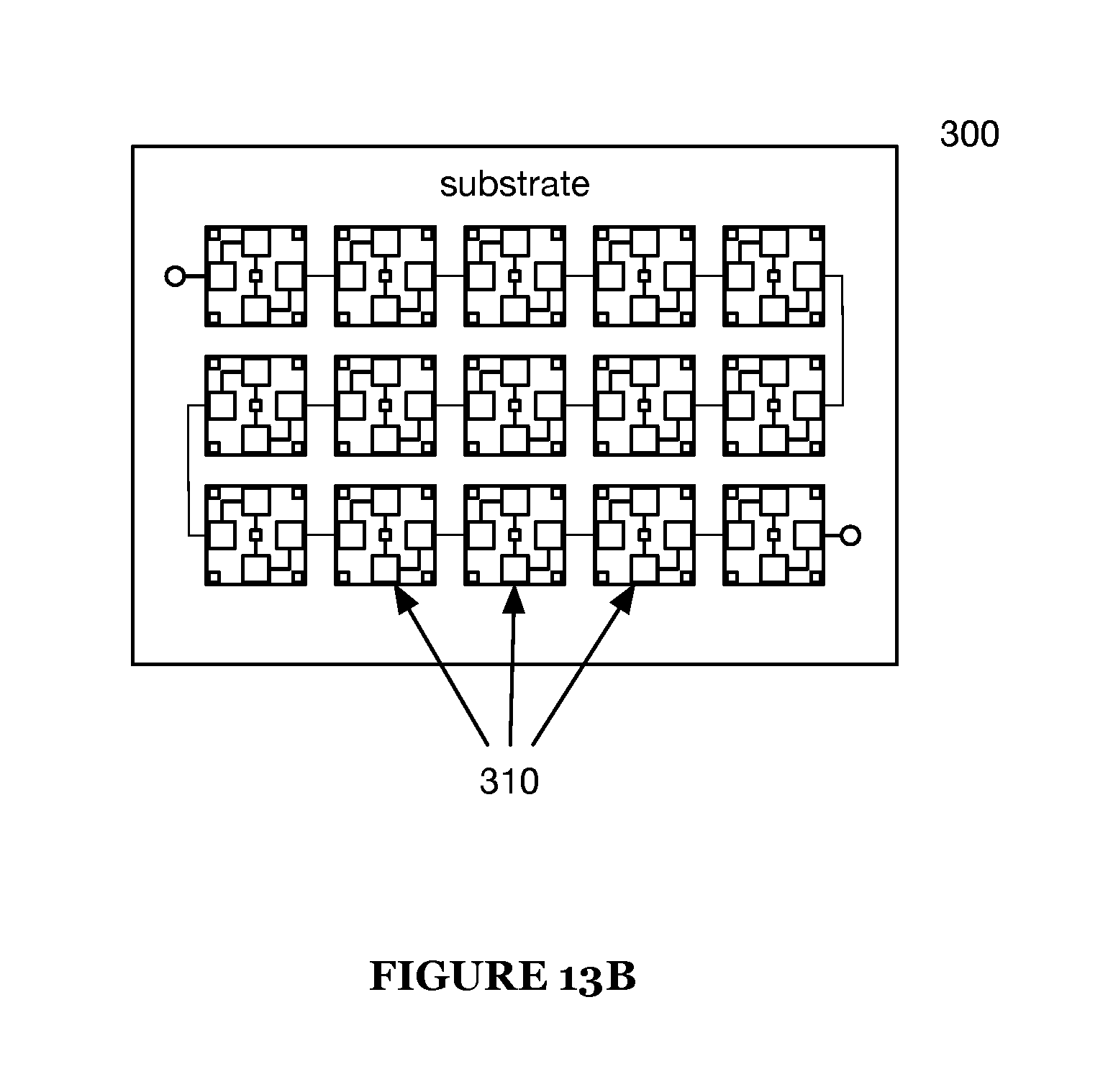
FIG. 13B is a schematic representation of a structure of a preferred embodiment;
FIG. 14A is a layer representation of a structure of a preferred embodiment; and
FIG. 14B is a layer representation of a structure of a preferred embodiment.
DESCRIPTION OF THE INVENTION EMBODIMENTS
The following description of the invention embodiments of the invention is not intended to limit the invention to these invention embodiments, but rather to enable any person skilled in the art to make and use this invention.
As mentioned in the background section, traditional delay elements face a number of issues in integration with RF circuits. One solution to the issues posed by traditional delay elements is found in the LC-resonator-based time delay filters of U.S. patent application Ser. No. 15/382,335, the entirety of which is incorporated by this reference.
The systems described herein may increase performance of full-duplex transceivers (and other applicable systems) by enabling high accuracy time delays without prohibitive increases in circuit complexity and/or cost. Other applicable systems include active sensing systems (e.g., RADAR), wired communications systems, wireless communications systems, channel emulators, filter skirt or stop band enhancements, reflectometers, PIM analyzers and/or any other suitable system, including communication systems where transmit and receive bands are close in frequency, but not overlapping.
The present application is directed to integration of similar resonator-based time delay filters in a modular configuration that enables their use in a space- and cost-effective manner. Such integrated filter modules may be useful in a variety of applications, including self-interference cancellation circuits.
As shown in FIG. 1, an integrated delay module (IDM) 100 includes LC resonator delays 11o and signal couplers 120. The LC resonator 110 delays are preferably static delays that can be selectively coupled into a signal path (using the signal couplers 120) to provide a discrete-step variable delay filter. Such coupling may occur dynamically (e.g., via switches that select between integrated delay module 100 outputs) or statically (e.g., delay modules 110 may be permanently wired to achieve different delays).
The IDM 100 is preferably modular in both intra-module and inter-module senses. In other words, the IDM 100 is preferably capable of achieving discretely variable time delays internally through access of various outputs. Likewise, multiple IDMs 100 may be daisy-chained to achieve even more delay options than a single IDM 100 can provide.
1. IDM Components
Each LC resonator delay 110 preferably includes a plurality of LC resonators 111. LC resonator delays 110 may additionally or alternatively include intra-filter coupling elements 112 and/or input matching elements 113.
The LC resonator delay 110 may additionally or alternatively include any number of LC resonators 111 (e.g., the set of LC resonators 111 may contain only a single LC resonator). The LC resonator delay 110 may additionally or alternatively include any suitable components coupled to the LC resonator(s) 111 that aid or otherwise contribute to the production of a time delay, such as passive or active components (e.g., capacitors, transistors, switches, etc.), integrated components (e.g., conductive layers and/or traces), or any other suitable components.
The LC resonator delay 110 preferably functions to produce a substantially frequency-invariant group delay for analog signals within a particular frequency band of interest; typically a frequency band within the radio frequency (RF) band, but alternatively any suitable frequency band. A group delay of an analog signal will delay the amplitude envelope of each frequency component of the signal; a frequency-invariant group delay will apply an equal time delay to the amplitude envelope of each frequency component of the signal.
The LC resonator delay 110 can additionally or alternatively function to increase the performance of signal transceivers (or other applicable systems; e.g., phased antenna arrays) by enabling high accuracy, adjustable, and/or reconfigurable group delay of signals without prohibitive increases in circuit complexity and/or cost.
The LC resonator delay 110 preferably has a relatively low and frequency-invariant (in a frequency band of interest) insertion loss, but may alternatively have any insertion loss and any frequency variation. The magnitude of the frequency response of the LC resonator delay 110 is substantially flat over the range of frequencies of interest (e.g., over the range of radio frequencies) and has a magnitude ripple that is small relative to the signal magnitude (e.g., 10.times., 100.times., or 1000.times. smaller). Alternatively, the LC resonator delay 110 may have any suitable insertion loss, and the response of the delay 110 may vary with frequency in any manner.
The LC resonator delay 110 is preferably constructed from lumped and/or distributed inductors and capacitors that are integrated into the substrate of a laminate (e.g., a printed circuit board), of a microchip (e.g., a silicon substrate, potentially realized by an integrated passive device (IPD) process), or any other suitable circuit substrate. Integration of the LC resonator delay 110 may substantially reduce cost and size of the LC resonator delay 110 and can further enable modularity of the IDM 100.
Portions of the delay 110 may additionally or alternatively be added to the substrate as discrete components. For example, the LC resonator(s) 111 of the delay 110 may be integrated into the substrate, and input matching element(s) 113 and/or intra-filter coupling element(s) 112 may be coupled to the substrate and/or the LC resonators as discrete components (e.g., via wire bonding, surface mounting, etc.).
The delay 110 is preferably implemented using analog circuitry, but additionally or alternatively may be implemented by digital circuitry or any combination of analog and digital circuitry. Analog circuitry is preferably implemented using a combination of the circuit substrate and metallized/conductive layers as described above, but can additionally or alternatively be implemented using analog integrated circuits (ICs) and/or discrete components (e.g., capacitors, inductors, resistors, transistors), wires, transmission lines, transformers, couplers, hybrids, waveguides, digital components, mixed-signal components, or any other suitable components. Digital circuitry is preferably implemented using a general-purpose processor, a digital signal processor, an application specific integrated circuit (ASIC), a field programmable gate array (FPGA) and/or any suitable processor(s) or circuit(s). The delay 110 is preferably preconfigured structurally to provide a given time delay or set of time delays, but may additionally or alternatively include memory to store configuration data, or be configured using externally stored configuration data or in any suitable manner.
The LC resonator delay 110 may include multiple coupling points (i.e., points at which other circuits may couple to the LC resonator delay 110) to enable either or both of variable impedance of the LC resonator delay 110 and variable delay of the LC resonator delay 110 (as discussed in subsequent sections). Coupling may be resistive (e.g., by a wire, metallized layer, or any other suitable conductive material), capacitive (e.g., by a discrete capacitor, mutual capacitance, etc.), inductive (e.g., by a discrete inductor, mutual inductance, etc.), electromagnetic (e.g., radiative coupling), or any other suitable manner. Additionally or alternatively, LC resonators 111 may be coupled to in any suitable manner.
The LC resonator delay 110 may also alter impedance or delay of the time LC resonator delay 110 through use of tunable elements in the LC resonators 111 or matching elements 113; i.e., as opposed to modifying impedance by coupling at a different coupling point, impedance may be modified using variable capacitors and/or inductors.
Each LC resonator 111 of the delay 110 functions to contribute a time delay to an input signal of the LC resonator delay 11o. As shown in FIG. 2, LC resonators 111 are preferably coupled in parallel; alternatively, LC resonators 111 may be coupled in any manner (e.g., series, combination of parallel and series, etc.). In such an implementation, the total delay experienced by a signal passing through the delay 110 may be adjustable by selecting the number of LC resonators 111 switched into the signal path. Alternatively, the delay 11o may have a number of LC resonators 111 with different frequency responses that may produce different time delays, and in such cases the delay of the time delay filter is preferably approximately equal to the sum of the time delay of each LC resonator 111 in the signal path.
Each LC resonator 111 of the delay 110 preferably has substantially the same frequency response and produces a substantially similar time delay. Accordingly, the delay of the LC resonator delay 11o is preferably approximately equal to the number of LC resonators 111 multiplied by the average time delay of the LC resonators 111. Alternatively, each LC resonator 111 may have any impedance and/or any time delay, and the LC resonator delay 11o may have any input/output impedance and total time delay.
Each LC resonator 111 preferably includes a substantially capacitive element (i.e., an element whose reactance, in a frequency band of interest, is negative) and a substantially inductive element (i.e., an element whose reactance, in a frequency band of interest, is positive) placed in parallel. Alternatively, each LC resonator 111 may include any circuit elements such that the impedance of the resonator 111 is approximately characterized by:
.function..omega..times..omega..omega..omega. ##EQU00001## where k is a constant
.times..times..times..times..times..times..times..times..times..times. ##EQU00002## and .omega..sub.0 is the resonant frequency of the resonator
.times..times..times..times..times..times..times..times..times..times..om- ega. ##EQU00003## Alternatively, the LC resonator may include circuit elements that are networked together to provide any suitable total impedance that varies as a function of frequency in any suitable manner.
The LC resonator 111 is preferably constructed in a laminate or chip substrate of the IDM 100 from a combination of metallization layer strips (e.g., strip inductor, microstrips, etc.), vias (e.g., through-hole vias, partial vias, buried vias, metallized slots, etc.), and the substrate itself. Additionally, the LC resonator 111 may include high-k dielectric layers. Alternatively, the LC resonator 111 may be constructed using any suitable materials.
The LC resonator 111 is preferably constructed from a combination of a parallel plate capacitor and a strip inductor on a laminate substrate. Such a parallel plate capacitor preferably includes a first conductive planar region separated from a second conductive planar region by a dielectric material, and the first and second conductive planar regions are preferably substantially parallel (e.g., as uniformly parallel as manufacturing tolerances may permit); however, a parallel plate capacitor may additionally or alternatively include any suitable subcomponents configured in any suitable manner. Alternatively, the LC resonator 111 may be constructed on a semiconductor/insulator chip substrate or from any other suitable capacitive/inductive elements (e.g., a spiral inductor or interdigitated finger capacitor). For example, an LC resonator 111 may include a braided inductive element (i.e., an inductive element comprising several inductive sub-elements in parallel, separated by an insulator, `braided` or otherwise positioned near each other). Such a braided inductive element is preferably formed from layers of the substrate including regions of alternately isolative and conductive material, which, when stacked together to form the substrate, are configured into a three-dimensional braided structure. Alternatively, a braided inductive element may be formed from any suitable materials, in any suitable manner.
An example implementation of an LC resonator 111 is as shown in FIG. 3 (cross-sectional view). In this implementation, the LC resonator 111 is constructed on a laminate substrate, having a number of isolative layers (1, 3-7, 9) and conductive layers (2, 8). The LC resonator 111 is formed from a parallel plate capacitor 11, of which a first plate is coupled to a ground plane 14 by a conductive via 10, and a strip inductor 12, which is coupled to the second plate of the capacitor 11 by a conductive via 10 and is coupled to the ground plane 14 by another conductive via 10. The ground plane may extend over all or most of the surface of the substrate on one side, and thus extend over a greater area than the strip inductor; alternatively, the ground plane may be a second strip inductor on the opposing side of the substrate that is of substantially the same size and extent, or may alternatively extend over any other suitable area. The resonator 111 may be coupled to at coupling point 13. If constructed on a laminate substrate, the LC resonator 111 may include any number of layers made of any material. For example, in this example implementation, the resonator 111 may include epoxy prepreg layers 4 and 6; FR-4 core layers 3, 7; copper conductive layers 2, 8; and hafnium oxide high-k dielectric layer 5, with copper vias 10. The layers, vias, and elements may be of any shape, size, thickness, etc. Note that in particular the dielectric material separating the plates of the capacitor (in this case layer 5) may be a standard isolative layer (e.g., a core layer), but may alternatively be a different dielectric material (e.g., a dielectric material with higher k or otherwise suitable to serve as an insulator for the capacitor 11).
LC resonators 111 may include multiple tapping (i.e., coupling) points to enable modification of the impedance of the LC resonator 111 (as seen by coupled or matching circuits). Additionally or alternatively, resonator 111 tapping may be used to modify impedance, time delay, resonance frequency, etc.
If a component of an LC resonator 111 includes multiple tapping points, they may be coupled to in any manner. For example, a switch (e.g., a transistor) may be coupled between a resonator 111 input and multiple tapping points, enabling a selection of tapping points. As another example, a switch may be coupled between tapping points, allowing those tapping points to be shorted.
If a component of an LC resonator 111 includes multiple tapping points and a coupling point at which it is coupled to other LC resonators (e.g., resistively coupled, capacitively coupled, inductively coupled, electromagnetically coupled), they may be selectively coupled in any suitable manner. For example, a set of switches (e.g., transistors, a multi-input/single-output multiplexer, etc.) may be coupled between the tapping points (taps) and the coupling point, enabling selection and/or adjustment of the impedance of the resonator as seen by components (e.g., resonators 111, matching elements) coupled to the coupling point.
In addition to having tapping points, LC resonators 111 may integrate or be coupled to tunable circuit elements (e.g., capacitors, inductors, transistors, resistors) to change their tuning properties. Tuning of the LC resonators 111 (and hence the delay filter) may also be done permanently during or at the end of the manufacturing process by adding (e.g. the use of 3D metal printing) or removing (e.g. milling metal away) material from traces, inductor or the plate of any capacitor in the circuit. Alternatively capacitors and/or inductors may be tuned by blowing small fuses implemented as traces in the substrate, adding or removing solder bridges, or adjusting the amount of insulating material on top, underneath, or on the side of the resonators.
As previously described, LC resonators 111 of the LC resonator delay 110 are preferably coupled in parallel to form the LC resonator delay 110 (or part of the LC resonator delay 110). While LC resonators 111 may be coupled in any manner (e.g., resistively), LC resonators 111 are preferably coupled to each other capacitively (using capacitive intra-filter coupling elements 112) and/or inductively (by positioning inductors of LC resonators 111 to enable magnetic coupling between the inductors) or in any combination of the coupling methods (e.g. 50% capacitive and 50% inductive).
Intra-filter elements 112 function to couple LC resonators 111 of the LC resonator delay 110. Similarly to components of the LC resonator 111, intra-filter elements are preferably passive capacitive, resistive, and/or inductive elements, but intra-filter elements may be any combination of active or passive components capable of coupling LC resonators 111. Intra-filter elements 112 are preferably constructed from a combination of metallization layer strips, vias, and the substrate, but may additionally or alternatively be constructed in any manner.
Input matching elements 113 function to couple LC resonators 111 to an input and/or output of the LC resonator delay 110 with a desired impedance. Input matching elements 113 preferably include circuits comprising passive capacitive, resistive, and/or inductive elements, but input matching elements 113 may be any active or passive combination of components capable of coupling the LC resonator delay 110 to an external circuit. Input matching elements 113 are preferably constructed from a combination of metallization layer strips, vias, and the substrate, but may additionally or alternatively be constructed in any manner.
The signal couplers 120, as shown in FIG. 4, function to couple LC resonator delays 110 of the IDM 100 (e.g., to each other, or to external signal paths). In general, the signal couplers 120 function to allow signals to be split and/or combined.
Signal couplers 120 preferably have a single input, but may additionally or alternatively have multiple inputs. Likewise, signal couplers 120 preferably have at least two outputs; a primary output (e.g., to direct a signal to another delay) and a secondary output (e.g., to enable mid-IDM 100 tapping of a signal). Additionally or alternatively, signal couplers may have multiple outputs (e.g., as shown in FIG. 4); this may be useful for MIMO circuits in which the delayed TX signal received from one transmitter is fed into different cancellers; each associated with a separate receive chain.
The signal coupler 120 may route power between inputs and outputs in any manner. For example, a signal coupler 120 may route the majority of power to a single output (of three outputs), or the signal coupler may split signals equally between the three outputs. The signal coupler 130 may have any number of input and output ports, including bidirectional input/output ports.
The signal coupler 120 is preferably a short section directional transmission line coupler, but may additionally or alternatively be any power divider, power combiner, directional coupler, or other type of signal splitter. The signal coupler 120 is preferably a passive coupler, but may additionally or alternatively be an active coupler (for instance, including amplifiers and/or switches). For example, the signal coupler 120 may comprise a coupled transmission line coupler, a branch-line coupler, a Lange coupler, a Wilkinson power divider, a hybrid coupler, a hybrid ring coupler, a multiple output divider, a waveguide directional coupler, a waveguide power coupler, a hybrid transformer coupler, a cross-connected transformer coupler, a resistive tee, and/or a resistive bridge hybrid coupler. The output ports of the signal coupler 120 are preferably not phase-shifted, but may additionally or alternatively be phase shifted by any amount (e.g., 90 degrees, 180 degrees).
In addition to the LC resonator delays 110 and the signal couplers 120, the IDM 100 may include any suitable components to connect or modify signals traveling in the IDM 100. For example, the IDM 100 may include amplifiers in between some LC resonator delays 110.
In an example implementation of a preferred embodiment, a delay 110 includes a substrate and an LC resonator 111. The substrate is a laminated circuit board that is comprised of several layers and has two broad, substantially parallel outer surfaces (e.g., a top and bottom surface, though the substrate may be in any suitable orientation). The resonator includes a capacitive element and an inductive element, coupled together into an LC circuit that is connected in parallel between a conductive contact point (e.g., a coupling point) on the first surface and a ground plane (e.g., a conductive region) on the second surface. The inductive element is a strip inductor that is formed by a conductive region (e.g., a metallized strip) on the first surface, and connected to the capacitive element and the ground plane by a pair of conductive vias. The first via is a through-hole via passing through the substrate (e.g., through several isolative and/or conductive layers of the substrate) to the ground plane, and the second via is a partial via that passes through the substrate to an intermediate position within the substrate where the capacitive element is located. There is also a third via that passes through the substrate between the capacitive element and the ground plane, and is directly electrically connected (e.g., soldered) to both. The capacitive element, which may be a parallel plate capacitor or any other suitable capacitive element, completes the LC circuit while interrupting the continuous conductive region (e.g., by way of a dielectric barrier between two sides, such as parallel plates, of the capacitive element). Together, the strip inductor, the first, second, and third vias, the capacitor, and the ground plane form a loop. This loop encloses an area that defines a normal axis, and the normal axis is substantially parallel to the plane(s) of the surfaces of the substrate; in other words, the conductive loop passes through the substrate in two locations (in this example, the locations of the vias) and lies adjacent to the substrate on two contralateral sides of the substrate.
In variations of a preferred embodiment, the LC resonators 111 may have a certain inductance and capacitance per unit length that repeats in a harmonic fashion over the length of the resonator, and the delay 110 may therefore be well-represented using a distributed inductor and capacitor model (e.g., a transmission line model). In other variations, the LC resonators 111 may be formed from localized discrete components (e.g., ceramic capacitors, on-chip capacitors, wound-wire inductors) such that the delay 110 is well-represented using a lumped-element model. In still further variations including a plurality of LC resonators, a subset of LC resonators may be represented by a distributed model and another subset of LC resonators may be represented by a lumped element model.
Note that in many cases, the positioning of resonators relative to one another and the coupling between resonators 111 (whether it be capacitive, magnetic, or both) may play into the performance of the delay 110. For example, resonators may be coupled in a large horseshoe pattern. Alternatively, resonators may be coupled in a meander pattern or a zigzag pattern. Resonators 111 may be positioned and coupled in any manner.
2. IDM Structure (Laminate)
The IDM 100 is preferably implemented as part of a multi-layer laminate structure 200, as shown in FIG. 5A. The laminate structure 200 preferably comprises a set of delay blocks 210, separated by interposer blocks 220 and coupled by a coupling block 230. Alternatively, there might also be an interposer block 220 between the upper most delay block 210 and the coupling block 230, as shown in FIG. 5B. Additionally or alternatively, the structure 200 may include any number of delay blocks 210, interposer blocks 220, and coupling blocks 230 (including zero).
The structure 200 functions as a particular implementation of the IDM 100, and thus is an analog time delay filter circuit.
Each block of the laminate structure 200 preferably includes multiple layers; additionally or alternatively, the laminate structure 200 may include single-layer blocks. Note that the term `block` as used throughout this application refers to a three-dimensional volume containing at least one circuit element (e.g., an inductive, capacitive, and/or resistive element). A block may represent the entirety of one or more layers or any sub-area or sub-volume of those layers. While blocks are generally shown in the FIGUREs of this specification as rectangular prisms, it is understood that they may be of any shape.
The term `block` is used due to the modular capability of the structure 200; blocks may be repeated (e.g., across a single layer or in different layers) to create such a modular structure. A `repeated` block is a block with an identical modular layout to another block (i.e., external connections are accessible at the same points relative to a coordinate system defined by the boundaries of the block). Using an identical modular layout across layers may mean, for instance, that the same photolithographic mask can be used for more than one layer. As another example, modular chips may be assembled (e.g., by a manufacturing robot) and electrically coupled (e.g., via soldering). As a third example, blocks may include physical connectors (e.g., pins/sockets), allowing modular structures to be assembled manually. Note that while two blocks may have an identical layout, those blocks may or may not have identical electrical characteristics. For example, one block may have identical layout to another block, but use a different material for the dielectric between plates of a parallel plate capacitor (changing response).
Components and connections of the laminate structure 200 are preferably constructed using selective etching of metallization layers of the laminate structure 200 and via filling, where metallization layers of the structure 200 are preferably separated by isolative layers and incident on a laminate substrate. Additionally or alternatively, components and connections of the laminate structure 200 may be fabricated in any manner (e.g., some components of the structure 200 may be contained on an integrated passive device (IPD) chip wire bonded or flip chip mounted to the laminate structure 200).
Preferably, the structure 200 is fabricated such that, with the interposers 220, all connections of the delay blocks 210 are electrically available to the coupling block 230. Alternatively, the structure 200 may be fabricated or configured in any manner.
The delay block 210 includes one or more time delays, as shown in FIG. 6. The delay block 210 is preferably fabricated to include pass-throughs (e.g., connections on the bottom layer of the block that are passed through to the top layer of the block), so that one configuration of the delay block 210 may be reused to generate multi-delay-layer structures 200 (further discussed in the section regarding interposer layers 220). Additionally or alternatively, the delay block 210 may include no such pass-throughs.
A pass-through is a connection that does not include any intentional reactive circuit elements (noting, of course, that any real-world physical connection has non-zero reactance). Such a pass-through preferably has substantially lower reactance (e.g., 10% or less) than an LC resonator used with said pass-through.
The time delays of the delay block 210 are preferably the LC resonator delay module 110, but may additionally or alternatively be any suitable time delay circuits.
In one implementation of a preferred embodiment, each delay block 210 includes two LC delay circuits, as shown in FIG. 7. In this implementation, the delay block 210 preferably includes a bottom ground-plane layer and three vertical ground walls-two on opposing sides of the delay block 210, and one between the two LC delay circuits (referred to as the center wall). Additionally or alternatively, the delay block 210 may include any suitable vertical grounding mechanism, or may include no such vertical grounding mechanism. Note that other blocks (e.g., the interposer circuit block 220, the coupling block 230, etc.) may also share ground walls or vertical grounding mechanisms with each other and/or with delay blocks 210.
The vertical ground walls function to couple the bottom ground-plane layer of the delay block 210 to bottom ground-plane layers of delay blocks 210 that may be stacked above it. The vertical ground walls may additionally or alternatively function to provide more convenient ground paths for delay components than may be available between said components and the bottom ground-plane layer. Further, the center ground wall may further function to isolate LC delay circuits of the delay block 210; for example, the center ground wall may be coupled to a ground shield that not only electrically and/or magnetically isolates a first LC delay circuit from a second LC delay circuit, but may additionally or alternatively electrically and/or magnetically isolate components of an LC delay circuit from other components of that same circuit (e.g., it may not be desired to have inductive coupling between the inductors as shown in FIG. 7).
The ground walls on the sidewalls of the laminate structure 200 are preferably metallized sidewalls of the delay block 210, but may additionally or alternatively be vias through the delay block 210, or any other conductive structure capable of coupling the bottom ground-plane layer of the delay block 210 to a bottom ground-plane layer of another delay block 210 (e.g., via an interposer block 220).
The center ground wall is preferably a set of vias (e.g., arranged in a single or double line, or as slots, separating two delays of the delay block 210) coupling the bottom ground-plane layer of the delay block 210 to a ground shield, but may additionally or alternatively be any other conductive structure capable of coupling the bottom ground-plane layer of the delay block 210 to a bottom ground-plane layer of another delay block 210 (e.g., via an interposer block 220).
In a variation of a preferred embodiment, some components of LC delays may be external to the delay block 210. For example, an LC delay may include one or more variable capacitors; in this example, the variable capacitors may be contained within an IPD die bonded or otherwise coupled to the structure 200.
Additionally or alternatively, IPD dies (or any other attached die, chip, or discrete component) may be used to add or integrate any of the components of the structure 200.
The interposer block 220 preferably functions to route connections of the delay block 210 so that delay blocks 210 having identical pinouts may be stacked on top of each other, resulting in a multiple-delay structure 200, as shown in FIG. 8. Additionally or alternatively, the interposer block 220 may route connections between delay blocks 210 (or any other blocks or layers of the structure 200) in any manner.
In a structure 200 including a lower delay block 210 and an upper delay block 210, the interposer 220 preferably remaps the input and output of the lower delay block 210 to pass-throughs of the upper delay block 210 (or vice versa).
The interposer block 220 preferably comprises hard-wired conductive coupling between delay blocks 210 above and below (or otherwise sandwiching the interposer block 220). The interposer block 220 may additionally or alternatively integrate any other components of the structure 200 (e.g., signal couplers, amplifiers, passive components, etc.).
The interposer block 220 preferably functions to route inputs and outputs from a first delay block 210 to a second delay block 210 in a two-delay-block structure 200, but may additionally or alternatively route inputs and outputs for any number of delay blocks 210; for example, for a three-block structure 200 with each delay block 210 including two sets of pass-throughs, as shown in FIG. 9.
The coupling block 230 includes one or more signal couplers (e.g., the signal couplers 120) and functions to provide access to delayers of the delay blocks 210, as shown in FIGS. 10A and 10B. The coupling block 230 may provide electrical access to delays in any manner (e.g., via metallic contacts arranged on a surface of the coupling block 230). The coupling block 230 may include multiple couplers, allowing the structure 200 to be coupled to at multiple points (in turn allowing the structure 200 to produce a discretely variable delay). For example, if each delay circuit is associated with a ions delay, OUT1 would result in a negligible delay, OUT2 would result in a ions delay, OUT3 in a 20 ns delay, OUT4 in a 30 ns delay, and OUT5 in an 40 ns delay.
The couplers of the coupling block 230 are preferably substantially similar to the couplers 120, but may additionally or alternatively be any suitable signal couplers.
As previously mentioned, the coupling block 230 may allow for delays of the structure 200 to be varied discretely. Such variance of delay may be accomplished in multiple manners. For example, outputs of the coupling block 230 of a first structure 200 (e.g., IN and OUT3) may be coupled (e.g., using wire bonding) to a first circuit, while outputs of the coupling block 230 of a second structure 200 (e.g., IN and OUT4) may be coupled to a second circuit (the two structures 200 having different, but static, delays).
As a second example, switches may be coupled to or integrated with the coupling block 230 (e.g., a transistor may switch between OUT4 and OUT5 as an output).
The IDM 200 may comprise any number of switches, and switches (or a set of switches) may be any suitable components capable of selectively coupling the taps and/or coupling points of delays 210, or other components to circuit common rails, grounds, and/or circuit inputs/outputs. For example, switches may include mechanical switches, mechanical relays, solid-state relays, transistors, silicon controlled rectifiers, triacs, and/or digital switches. Switches of the set of switches may be operable electronically by a tuning circuit or other suitable controller, but may additionally or alternatively be set in any manner. For example, switches may be manually set by a circuit user. As another example, switches may be one-time-use junctions that are configured into a desired configuration when the delay 210 is manufactured (e.g., by soldering, annealing, fusing, cutting or any other suitable manner of irreversible configuration), resulting in a desired overall delay 210 configuration (e.g., group delay value).
Switches are preferably operable between one or more switch states, in which a state of the switch corresponds to coupling between two or more system components. For example, a switch (e.g., transistor) may be operable in a first switch state that couples a first tapping point to a coupling point of a resonator, and in a second switch state that couples a second tapping point to a coupling point of a resonator. In another example, a switch may be operable in a first switch state that couples one of a set of resonators to a common rail (e.g., a ground plane) of the system, in order to place it in the signal path of a signal passing through the time delay filter; this switch may be operable in a second switch state that decouples the resonator from the common rail, thereby removing the resonator from the signal path (and reducing the overall time delay applied by the time delay filter).
As a third example, the coupling block 230 may include bridging links or contacts; that is, links between contacts of the coupling block 230 that may be bridged to modify the circuit architecture of the coupling block 230, as shown in FIGS. 11A and 11B. In this example, the coupling block 230 may include a set of closely spaced contacts that may be bridged (e.g., with a solder ball or other conductive deposition); alternatively or additionally, the coupling block 230 may include a bridge that may be selectively milled, etched, laser cut, etc. (as shown in FIGS. 12A and 12B). The coupling block 230 may additionally or alternatively include any set of electrical coupling points that may be modified by the addition or removal of conductive and/or isolative material.
The coupling block 230 may additionally or alternatively include circuit components desired to be inserted in the structure 200 signal path; for example, an amplifier as shown in FIGS. 12A and 12B. The coupling block 230 may include any suitable circuits or circuit components; e.g., transistors, capacitors, resistors, inductors, phase shift circuits, attenuators, amplifiers, etc.
As previously discussed, the structure 200 is preferably modular both intra-module (e.g., a modular delay may be constructed by selectively using outputs of a given structure 200) and inter-module (e.g., outputs of one structure 200 may be coupled to inputs of another structure 200, and so on, to create daisy-chained delays).
Note that while the structure 200 is described as a laminate structure, the structure 200 may additionally or alternatively be any multi-layer structure having delay blocks 210.
3. IDM Structure (IPD)
The IDM 100 may additionally or alternatively be implemented using an integrated passive device (IPD) process (or using another on-wafer fabrication process). In this embodiment, the IDM 100 is preferably implemented as part of an IPD structure 300 that comprises a set of delay blocks 310. The structure 300 functions as a particular implementation of the IDM 100, and thus is an analog time delay filter circuit.
Each block of the structure 300 preferably includes multiple layers; additionally or alternatively, the structure 300 may include single-layer blocks. Note that the term `block` as used throughout this application refers to a three-dimensional volume containing at least one circuit element (e.g., an inductive, capacitive, and/or resistive element). A block may represent the entirety of one or more layers or any sub-area or sub-volume of those layers. While blocks are generally shown in the FIGUREs of this specification as rectangular prisms, it is understood that they may be of any shape.
The term `block` is used due to the modular capability of the structure 300; blocks may be repeated (e.g., across a single layer or in different layers) to create such a modular structure. A `repeated` block is a block with an identical modular layout to another block (i.e., external connections are accessible at the same points relative to a coordinate system defined by the boundaries of the block). Using an identical modular layout across layers may mean, for instance, that the same photolithographic mask can be used for more than one layer. As another example, modular chips may be assembled (e.g., by a manufacturing robot) and electrically coupled (e.g., via soldering). As a third example, blocks may include physical connectors (e.g., pins/sockets), allowing modular structures to be assembled manually. Note that while two blocks may have an identical layout, those blocks may or may not have identical electrical characteristics. For example, one block may have identical layout to another block, but use a different material for the dielectric between plates of a parallel plate capacitor (changing response).
The delay block 310 includes one or more time delays, as shown in FIG. 13A (delays labeled as LC1, LC2 . . . ). The delay block 310 is preferably fabricated to include pass-throughs (e.g., connections on the bottom layer of the block that are passed through to the top layer of the block). While it is possible to layer delay blocks 310 in a similar manner to the structure 200, these passthroughs may additionally or alternatively used to pass signals/power from an underlying structure (e.g., an RF communications PCB) to a different chip atop the structure 300 (e.g., a CMOS chip or another IPD chip). Alternatively, the delay block 310 may include no such pass-throughs.
A pass-through is a connection that does not include any intentional reactive circuit elements (noting, of course, that any real-world physical connection has non-zero reactance). Such a pass-through preferably has substantially lower reactance (e.g., 10% or less) than an LC resonator used with said pass-through.
The time delays of the delay block 310 are preferably the LC resonator delay module 110, but may additionally or alternatively be any suitable time delay circuits.
The small size of the IPD structure may make it advantageous to array many blocks 310, for example as shown in FIG. 13B.
IPD structures 300 may be fabricated using any fabrication technology; for example, via masked etching and deposition on a silicon, alumina, or silica substrate. Likewise, IPD structures 300 may be packaged in any manner (e.g., wire bondable or flip-chip mountable).
The IPD structure 300 may additionally or alternatively include interposer blocks 320 (substantially similar to interposer blocks 220, but constructed using an IPD or similar process), but the function of the interposer blocks may alternatively be performed by a combination of the delay blocks 310 (which may include pass-throughs or taps; i.e., connection points to a circuit of a delay block 310) and an overlying chip. For example, a CMOS chip may be mounted to the IPD structure 300 using flip-chip assembly. By selectively placing solder balls or copper pillars, the CMOS chip can be selectively connected to the IPD structure 300 (or to underlying circuits via pass-throughs), as shown in FIGS. 14A and 14B.
Note that in general, the circuitry connected to the active side of the IPD structure 300 (the active side is the side with the majority of circuitry; e.g., the side shown contacting the PCB in FIGS. 14A and 14B) may be referred to as a primary coupled circuit (e.g., in the case of FIGS. 14A and 14B, the primary coupled circuit is a PCB), which circuitry connected to the other side of the structure 300 (e.g., the CMOS chip in FIG. 14A, or another IPD structure) may be referred to as a secondary coupled circuit. The terms "primary coupled circuit" and "secondary coupled circuit" are not intended to have additional meaning besides as described here.
The structure 300 may comprise any number of switches, and switches (or a set of switches) may be any suitable components capable of selectively coupling the taps and/or coupling points of delays 310, or other components to circuit common rails, grounds, and/or circuit inputs/outputs. For example, switches may include mechanical switches, mechanical relays, solid-state relays, transistors, silicon controlled rectifiers, triacs, and/or digital switches. Switches of the set of switches may be operable electronically by a tuning circuit or other suitable controller, but may additionally or alternatively be set in any manner. For example, switches may be manually set by a circuit user. As another example, switches may be one-time-use junctions that are configured into a desired configuration when the delay 310 is manufactured (e.g., by soldering, annealing, fusing, cutting or any other suitable manner of irreversible configuration), resulting in a desired overall delay 310 configuration (e.g., group delay value).
Switches are preferably operable between one or more switch states, in which a state of the switch corresponds to coupling between two or more system components. For example, a switch (e.g., transistor) may be operable in a first switch state that couples a first tapping point to a coupling point of a resonator, and in a second switch state that couples a second tapping point to a coupling point of a resonator. In another example, a switch may be operable in a first switch state that couples one of a set of resonators to a common rail (e.g., a ground plane) of the system, in order to place it in the signal path of a signal passing through the time delay filter; this switch may be operable in a second switch state that decouples the resonator from the common rail, thereby removing the resonator from the signal path (and reducing the overall time delay applied by the time delay filter).
Similar to the structure 200, the structure 300 may include bridging links or contacts; e.g., such that may be bridged by solder balls used in the flip chip assembly process.
As previously discussed, the structure 300 is preferably modular both intra-module (e.g., a modular delay may be constructed by selectively using outputs of a given structure 300) and inter-module (e.g., outputs of one structure 300 may be coupled to inputs of another structure 300, and so on, to create daisy-chained delays).
Note that while the structure 300 is described as an IPD structure, the structure 300 may additionally or alternatively be any multi-layer structure having delay blocks 310.
The methods of the preferred embodiment and variations thereof can be embodied and/or implemented at least in part as a machine configured to receive a computer-readable medium storing computer-readable instructions. The instructions are preferably executed by computer-executable components preferably integrated with an analog time delay filter circuit. The computer-readable medium can be stored on any suitable computer-readable media such as RAMs, ROMs, flash memory, EEPROMs, optical devices (CD or DVD), hard drives, floppy drives, or any suitable device. The computer-executable component is preferably a general or application specific processor, but any suitable dedicated hardware or hardware/firmware combination device can alternatively or additionally execute the instructions.
As a person skilled in the art will recognize from the previous detailed description and from the figures and claims, modifications and changes can be made to the preferred embodiments of the invention without departing from the scope of this invention defined in the following claims.
* * * * *
D00000
D00001
D00002
D00003
D00004
D00005
D00006
D00007
D00008
D00009
D00010
D00011
D00012

D00013

D00014

D00015

D00016

D00017
D00018

M00001

M00002

M00003

XML
uspto.report is an independent third-party trademark research tool that is not affiliated, endorsed, or sponsored by the United States Patent and Trademark Office (USPTO) or any other governmental organization. The information provided by uspto.report is based on publicly available data at the time of writing and is intended for informational purposes only.
While we strive to provide accurate and up-to-date information, we do not guarantee the accuracy, completeness, reliability, or suitability of the information displayed on this site. The use of this site is at your own risk. Any reliance you place on such information is therefore strictly at your own risk.
All official trademark data, including owner information, should be verified by visiting the official USPTO website at www.uspto.gov. This site is not intended to replace professional legal advice and should not be used as a substitute for consulting with a legal professional who is knowledgeable about trademark law.