Methods of forming semiconductor devices including tunnel barrier materials
Siddik , et al. O
U.S. patent number 10,439,131 [Application Number 14/597,903] was granted by the patent office on 2019-10-08 for methods of forming semiconductor devices including tunnel barrier materials. This patent grant is currently assigned to Micron Technology, Inc.. The grantee listed for this patent is Micron Technology, Inc.. Invention is credited to Witold Kula, Suresh Ramarajan, Manzar Siddik.


| United States Patent | 10,439,131 |
| Siddik , et al. | October 8, 2019 |
| **Please see images for: ( Certificate of Correction ) ** |
Methods of forming semiconductor devices including tunnel barrier materials
Abstract
A semiconductor device comprises an array of magnetic cell structures each comprising a magnetic tunnel junction over an electrode on a substrate. Each of the magnetic tunnel junctions includes a magnetic material over the substrate, a first tunnel barrier material over the magnetic material, a second tunnel barrier material over the annealed first tunnel barrier material, and another magnetic material over the second tunnel barrier material. Each magnetic tunnel junction is configured to exhibit a tunnel magnetoresistance greater than or equal to about 180% at a resistance area product of less than about 8 ohm .mu.m.sup.2. The semiconductor device also includes another electrode over the another magnetic material. Semiconductor devices including the magnetic tunnel junctions, methods of forming the magnetic tunnel junctions, and methods of forming semiconductor devices including the magnetic tunnel junctions are disclosed.
| Inventors: | Siddik; Manzar (Singapore, SG), Kula; Witold (Gilroy, CA), Ramarajan; Suresh (Singapore, SG) | ||||||||||
|---|---|---|---|---|---|---|---|---|---|---|---|
| Applicant: |
|
||||||||||
| Assignee: | Micron Technology, Inc. (Boise,
ID) |
||||||||||
| Family ID: | 56406222 | ||||||||||
| Appl. No.: | 14/597,903 | ||||||||||
| Filed: | January 15, 2015 |
Prior Publication Data
| Document Identifier | Publication Date | |
|---|---|---|
| US 20160211440 A1 | Jul 21, 2016 | |
| Current U.S. Class: | 1/1 |
| Current CPC Class: | G11C 11/161 (20130101); H01L 43/12 (20130101); H01L 43/08 (20130101) |
| Current International Class: | H01L 43/12 (20060101); H01L 43/08 (20060101); G11C 11/16 (20060101) |
References Cited [Referenced By]
U.S. Patent Documents
| 4882936 | November 1989 | Garshelis |
| 5551586 | September 1996 | Uenoyama et al. |
| 5563000 | October 1996 | Tukaram et al. |
| 5565266 | October 1996 | Hatwar et al. |
| 5583725 | December 1996 | Coffey et al. |
| 5604030 | February 1997 | Yamane |
| 5768069 | June 1998 | Mauri |
| 6166948 | December 2000 | Parkin et al. |
| 6258470 | July 2001 | Sakakima et al. |
| 6275363 | August 2001 | Gill |
| 6347049 | February 2002 | Childress et al. |
| 6363000 | March 2002 | Perner et al. |
| 6387476 | May 2002 | Iwasaki et al. |
| 6483741 | November 2002 | Iwasaki et al. |
| 6560135 | May 2003 | Matsuoka et al. |
| 6569545 | May 2003 | Tetsuya et al. |
| 6611405 | August 2003 | Inomata et al. |
| 6653704 | November 2003 | Gurney et al. |
| 6703249 | March 2004 | Okazawa et al. |
| 6771534 | August 2004 | Stipe |
| 6806096 | October 2004 | Kim et al. |
| 6845038 | January 2005 | Shukh |
| 6955857 | October 2005 | Kubota |
| 6964819 | November 2005 | Girt |
| 6970376 | November 2005 | Fukuzumi |
| 6980468 | December 2005 | Ounadjela |
| 6992359 | January 2006 | Nguyen et al. |
| 6998150 | February 2006 | Li et al. |
| 7026671 | April 2006 | Mizuguchi et al. |
| 7095933 | August 2006 | Barth |
| 7130167 | October 2006 | Gill |
| 7189583 | March 2007 | Drewes |
| 7230265 | June 2007 | Kaiser et al. |
| 7239489 | July 2007 | Lin et al. |
| 7274080 | September 2007 | Parkin |
| 7372674 | May 2008 | Gill |
| 7378698 | May 2008 | Ha et al. |
| 7379280 | May 2008 | Fukumoto et al. |
| 7486552 | February 2009 | Apalkov et al. |
| 7488609 | February 2009 | Lin |
| 7514160 | April 2009 | Nagahama et al. |
| 7563486 | July 2009 | Barth |
| 7564152 | July 2009 | Clark et al. |
| 7602033 | October 2009 | Zhao et al. |
| 7660153 | February 2010 | Yamane et al. |
| 7682841 | March 2010 | Dahmani et al. |
| 7732881 | June 2010 | Wang |
| 7750421 | July 2010 | Horng et al. |
| 7791844 | September 2010 | Carey et al. |
| 7835173 | November 2010 | Ma et al. |
| 7863060 | January 2011 | Belen et al. |
| 7885105 | February 2011 | Li et al. |
| 7919794 | April 2011 | Gu et al. |
| 7929370 | April 2011 | Min |
| 7932572 | April 2011 | Tsujiuchi |
| 7948044 | May 2011 | Horng et al. |
| 8009465 | August 2011 | Nakayama et al. |
| 8043732 | October 2011 | Anderson et al. |
| 8048492 | November 2011 | Fukuzawa et al. |
| 8068317 | November 2011 | Gill |
| 8080432 | December 2011 | Horng et al. |
| 8089137 | January 2012 | Lung et al. |
| 8102700 | January 2012 | Liu et al. |
| 8120949 | February 2012 | Ranjan et al. |
| 8138561 | March 2012 | Horng et al. |
| 8223539 | July 2012 | Smythe et al. |
| 8324697 | December 2012 | Worledge |
| 8334148 | December 2012 | Jeong et al. |
| 8338004 | December 2012 | Shin et al. |
| 8357962 | January 2013 | Marukame et al. |
| 8385107 | February 2013 | Prejbeanu |
| 8411498 | April 2013 | Kim et al. |
| 8422286 | April 2013 | Ranjan et al. |
| 8470462 | June 2013 | Horng et al. |
| 8487390 | July 2013 | Dimitrov et al. |
| 8492169 | July 2013 | Cao |
| 8514527 | August 2013 | Komagaki et al. |
| 8545999 | October 2013 | Leng et al. |
| 8570798 | October 2013 | Meade et al. |
| 8587043 | November 2013 | Natori et al. |
| 8604573 | December 2013 | Yamakawa et al. |
| 8623452 | January 2014 | Zhou |
| 8692342 | April 2014 | Oh et al. |
| 8704320 | April 2014 | Zhu et al. |
| 8749003 | June 2014 | Horng et al. |
| 8766341 | July 2014 | Han et al. |
| 8779538 | July 2014 | Chen et al. |
| 8790798 | July 2014 | Shukh |
| 8803265 | August 2014 | Lim et al. |
| 8823118 | September 2014 | Horng et al. |
| 8854876 | October 2014 | Uchida et al. |
| 8923038 | December 2014 | Kula et al. |
| 9269888 | February 2016 | Meade et al. |
| 9373780 | June 2016 | Jan et al. |
| 9466789 | October 2016 | Wang et al. |
| 9472752 | October 2016 | Wang et al. |
| 9705075 | July 2017 | Lim et al. |
| 9786841 | October 2017 | Siddik et al. |
| 10014466 | July 2018 | Siddik et al. |
| 2001/0024853 | September 2001 | Wallace et al. |
| 2002/0089874 | July 2002 | Nickel et al. |
| 2002/0097534 | July 2002 | Sun et al. |
| 2002/0105827 | August 2002 | Redon et al. |
| 2002/0114112 | August 2002 | Nakashio et al. |
| 2003/0011939 | January 2003 | Gill |
| 2003/0030434 | February 2003 | Hasegawa et al. |
| 2003/0035255 | February 2003 | Hasegawa et al. |
| 2003/0063415 | April 2003 | Hasegawa et al. |
| 2003/0064569 | April 2003 | Takayama et al. |
| 2003/0103371 | June 2003 | Kim et al. |
| 2003/0142562 | July 2003 | Kreupl |
| 2003/0199104 | October 2003 | Leuschner et al. |
| 2004/0008455 | January 2004 | Hasegawa et al. |
| 2004/0075959 | April 2004 | Gill |
| 2004/0091744 | May 2004 | Carey et al. |
| 2004/0144995 | July 2004 | Nagahama et al. |
| 2004/0174740 | September 2004 | Lee et al. |
| 2004/0224243 | November 2004 | Yoshizawa et al. |
| 2004/0233760 | November 2004 | Guo et al. |
| 2004/0246776 | December 2004 | Covington |
| 2005/0019608 | January 2005 | Kim et al. |
| 2005/0024786 | February 2005 | Gill et al. |
| 2005/0036361 | February 2005 | Fukuzumi |
| 2005/0068683 | March 2005 | Gill |
| 2005/0087511 | April 2005 | Sharma et al. |
| 2005/0106810 | May 2005 | Pakala et al. |
| 2005/0164414 | July 2005 | Deak |
| 2005/0173698 | August 2005 | Drewes |
| 2005/0189574 | September 2005 | Nguyen et al. |
| 2005/0211973 | September 2005 | Mori et al. |
| 2005/0230743 | October 2005 | Nakagawa et al. |
| 2005/0231853 | October 2005 | Li et al. |
| 2005/0233174 | October 2005 | Munteanu et al. |
| 2005/0276099 | December 2005 | Horng et al. |
| 2006/0002039 | January 2006 | Hasegawa et al. |
| 2006/0038213 | February 2006 | Mori et al. |
| 2006/0042930 | March 2006 | Mauri |
| 2006/0098354 | May 2006 | Parkin |
| 2006/0114714 | June 2006 | Kanegae |
| 2006/0118842 | June 2006 | Iwata |
| 2006/0261425 | November 2006 | Suemitsu et al. |
| 2007/0008661 | January 2007 | Min et al. |
| 2007/0026260 | February 2007 | Nemoto et al. |
| 2007/0026263 | February 2007 | Kubota |
| 2007/0035890 | February 2007 | Sbiaa |
| 2007/0053112 | March 2007 | Papworth Parkin |
| 2007/0086121 | April 2007 | Nagase et al. |
| 2007/0132003 | June 2007 | Takashima et al. |
| 2007/0201265 | August 2007 | Ranjan et al. |
| 2007/0217071 | September 2007 | Inamura et al. |
| 2007/0247756 | October 2007 | Lai et al. |
| 2007/0253116 | November 2007 | Takahashi |
| 2007/0297220 | December 2007 | Yoshikawa et al. |
| 2008/0164502 | July 2008 | Fukumoto et al. |
| 2008/0164548 | July 2008 | Ranjan et al. |
| 2008/0170329 | July 2008 | Thangaraj et al. |
| 2008/0179699 | July 2008 | Horng et al. |
| 2008/0182131 | July 2008 | Iwasaki |
| 2008/0198512 | August 2008 | Mukai |
| 2008/0205130 | August 2008 | Sun et al. |
| 2008/0225581 | September 2008 | Yamane et al. |
| 2008/0242088 | October 2008 | Suzuki |
| 2008/0253039 | October 2008 | Nagamine et al. |
| 2008/0278867 | November 2008 | Fukumoto et al. |
| 2009/0039450 | February 2009 | Lee et al. |
| 2009/0079018 | March 2009 | Nagase et al. |
| 2009/0096043 | April 2009 | Min et al. |
| 2009/0108383 | April 2009 | Horng et al. |
| 2009/0168238 | July 2009 | Kim et al. |
| 2009/0180215 | July 2009 | Ishikawa et al. |
| 2009/0190262 | July 2009 | Murakami et al. |
| 2009/0195924 | August 2009 | Nemoto |
| 2009/0218645 | September 2009 | Ranjan et al. |
| 2009/0229111 | September 2009 | Zhao et al. |
| 2009/0231909 | September 2009 | Dieny et al. |
| 2009/0250776 | October 2009 | Takenaga et al. |
| 2009/0251829 | October 2009 | Zhang et al. |
| 2009/0257151 | October 2009 | Zhang et al. |
| 2010/0034014 | February 2010 | Ohno et al. |
| 2010/0035085 | February 2010 | Jung et al. |
| 2010/0080036 | April 2010 | Liu et al. |
| 2010/0080048 | April 2010 | Liu et al. |
| 2010/0086809 | April 2010 | Kuboki |
| 2010/0096716 | April 2010 | Ranjan et al. |
| 2010/0102406 | April 2010 | Xi et al. |
| 2010/0109110 | May 2010 | Wang et al. |
| 2010/0110783 | May 2010 | Liu et al. |
| 2010/0140726 | June 2010 | Apalkov et al. |
| 2010/0148167 | June 2010 | Whig et al. |
| 2010/0171086 | July 2010 | Lung et al. |
| 2010/0176472 | July 2010 | Shoji |
| 2010/0177557 | July 2010 | Liu et al. |
| 2010/0177561 | July 2010 | Liu et al. |
| 2010/0200899 | August 2010 | Marukame et al. |
| 2010/0219491 | September 2010 | Lee et al. |
| 2010/0220516 | September 2010 | Lee et al. |
| 2010/0230769 | September 2010 | Ozaki et al. |
| 2010/0240151 | September 2010 | Belen et al. |
| 2010/0276771 | November 2010 | Fukumoto et al. |
| 2010/0327248 | December 2010 | Khoueir et al. |
| 2010/0328822 | December 2010 | Park et al. |
| 2011/0007429 | January 2011 | Dimitrov et al. |
| 2011/0007543 | January 2011 | Khoury |
| 2011/0014500 | January 2011 | Horng et al. |
| 2011/0031569 | February 2011 | Watts et al. |
| 2011/0049657 | March 2011 | Tsukamoto et al. |
| 2011/0049658 | March 2011 | Zheng et al. |
| 2011/0051503 | March 2011 | Hu et al. |
| 2011/0062537 | March 2011 | Oh et al. |
| 2011/0064969 | March 2011 | Chen et al. |
| 2011/0086439 | April 2011 | Choi |
| 2011/0096443 | April 2011 | Zhang et al. |
| 2011/0121366 | May 2011 | Or-Bach et al. |
| 2011/0145514 | June 2011 | Lee et al. |
| 2011/0149646 | June 2011 | Liu et al. |
| 2011/0149647 | June 2011 | Kim et al. |
| 2011/0149670 | June 2011 | Heo et al. |
| 2011/0151280 | June 2011 | Takahashi et al. |
| 2011/0170339 | July 2011 | Wunderlich et al. |
| 2011/0170341 | July 2011 | Butler |
| 2011/0194329 | August 2011 | Ohba et al. |
| 2011/0241138 | October 2011 | Hsieh et al. |
| 2011/0260274 | October 2011 | Zheng et al. |
| 2011/0266642 | November 2011 | Viala et al. |
| 2011/0269251 | November 2011 | Kim et al. |
| 2011/0293967 | December 2011 | Zhang et al. |
| 2011/0298456 | December 2011 | Lu et al. |
| 2011/0303995 | December 2011 | Worledge |
| 2011/0303997 | December 2011 | Wang et al. |
| 2011/0309418 | December 2011 | Nakayama et al. |
| 2012/0012952 | January 2012 | Chen et al. |
| 2012/0012953 | January 2012 | Lottis et al. |
| 2012/0012954 | January 2012 | Yamada et al. |
| 2012/0015099 | January 2012 | Sun et al. |
| 2012/0018823 | January 2012 | Huai et al. |
| 2012/0018825 | January 2012 | Lim et al. |
| 2012/0040207 | February 2012 | Horng et al. |
| 2012/0061781 | March 2012 | Ohmori et al. |
| 2012/0068139 | March 2012 | Daibou et al. |
| 2012/0069647 | March 2012 | Kramer et al. |
| 2012/0074511 | March 2012 | Takahashi et al. |
| 2012/0075922 | March 2012 | Yamada et al. |
| 2012/0075927 | March 2012 | Chen et al. |
| 2012/0106233 | May 2012 | Katti |
| 2012/0112297 | May 2012 | Yamakawa et al. |
| 2012/0134201 | May 2012 | Ogimoto |
| 2012/0135273 | May 2012 | Horng et al. |
| 2012/0146167 | June 2012 | Huai et al. |
| 2012/0155156 | June 2012 | Watts et al. |
| 2012/0164485 | June 2012 | Lin |
| 2012/0181537 | July 2012 | Cao et al. |
| 2012/0205758 | August 2012 | Jan et al. |
| 2012/0217594 | August 2012 | Kajiyama |
| 2012/0217599 | August 2012 | Nam et al. |
| 2012/0218813 | August 2012 | Oh et al. |
| 2012/0225499 | September 2012 | Nozieres et al. |
| 2012/0236631 | September 2012 | Park et al. |
| 2012/0241878 | September 2012 | Hu et al. |
| 2012/0241879 | September 2012 | Ikeno et al. |
| 2012/0261777 | October 2012 | Shukh |
| 2012/0267733 | October 2012 | Hu et al. |
| 2012/0280336 | November 2012 | Jan et al. |
| 2012/0286382 | November 2012 | Jan et al. |
| 2012/0299134 | November 2012 | Jan et al. |
| 2012/0299137 | November 2012 | Worledge |
| 2013/0005052 | January 2013 | Hu et al. |
| 2013/0015539 | January 2013 | Choi |
| 2013/0028013 | January 2013 | Ikeda et al. |
| 2013/0032911 | February 2013 | Jung et al. |
| 2013/0042081 | February 2013 | Park et al. |
| 2013/0043471 | February 2013 | Cao et al. |
| 2013/0059168 | March 2013 | Tahmasebi et al. |
| 2013/0064011 | March 2013 | Liu et al. |
| 2013/0069185 | March 2013 | Saida et al. |
| 2013/0075839 | March 2013 | Chen et al. |
| 2013/0134534 | May 2013 | Sbiaa et al. |
| 2013/0140658 | June 2013 | Yamane et al. |
| 2013/0146996 | June 2013 | Yu et al. |
| 2013/0148418 | June 2013 | Luo et al. |
| 2013/0177781 | July 2013 | Chepulskyy et al. |
| 2013/0209836 | August 2013 | Ataka et al. |
| 2013/0221459 | August 2013 | Jan et al. |
| 2013/0224521 | August 2013 | Wang et al. |
| 2013/0228884 | September 2013 | Zheng et al. |
| 2013/0229866 | September 2013 | Ranjan et al. |
| 2013/0236639 | September 2013 | Carey et al. |
| 2013/0242435 | September 2013 | Fuji et al. |
| 2013/0250661 | September 2013 | Sandhu et al. |
| 2013/0288392 | October 2013 | Nozieres et al. |
| 2013/0313665 | November 2013 | Rhie et al. |
| 2013/0314815 | November 2013 | Yuan et al. |
| 2013/0334630 | December 2013 | Kula et al. |
| 2013/0334631 | December 2013 | Kinney et al. |
| 2014/0008742 | January 2014 | Chen et al. |
| 2014/0015076 | January 2014 | Gan et al. |
| 2014/0021426 | January 2014 | Lee et al. |
| 2014/0027869 | January 2014 | Lee et al. |
| 2014/0038312 | February 2014 | Lee et al. |
| 2014/0063656 | March 2014 | Hashimoto |
| 2014/0064047 | March 2014 | Niwa et al. |
| 2014/0070341 | March 2014 | Beach et al. |
| 2014/0084398 | March 2014 | Oguz et al. |
| 2014/0099735 | April 2014 | Horng et al. |
| 2014/0116984 | May 2014 | Ding et al. |
| 2014/0151843 | June 2014 | Millward et al. |
| 2014/0157065 | June 2014 | Ong |
| 2014/0217526 | August 2014 | Guo |
| 2014/0242419 | August 2014 | Singh et al. |
| 2014/0264663 | September 2014 | Chen et al. |
| 2014/0268301 | September 2014 | Ding et al. |
| 2014/0269064 | September 2014 | Jeon |
| 2014/0272454 | September 2014 | Zhang et al. |
| 2014/0287537 | September 2014 | Shukh |
| 2014/0293436 | October 2014 | Nagahama et al. |
| 2014/0308542 | October 2014 | Zhang et al. |
| 2014/0327095 | November 2014 | Kim et al. |
| 2014/0334032 | November 2014 | Nishioka et al. |
| 2014/0339504 | November 2014 | Kim et al. |
| 2014/0367814 | December 2014 | Ohmori et al. |
| 2015/0028439 | January 2015 | Kula et al. |
| 2015/0041933 | February 2015 | Chepulskyy et al. |
| 2015/0069556 | March 2015 | Yamakawa et al. |
| 2015/0076485 | March 2015 | Sandhu et al. |
| 2015/0076633 | March 2015 | Siddik et al. |
| 2015/0179916 | June 2015 | Pramanik |
| 2015/0249202 | September 2015 | Siddik et al. |
| 2015/0270478 | September 2015 | Annunziata et al. |
| 2015/0287910 | October 2015 | Lu et al. |
| 2015/0295164 | October 2015 | Sandhu et al. |
| 2015/0340601 | November 2015 | Huai et al. |
| 2016/0005954 | January 2016 | Erickson et al. |
| 2016/0086645 | March 2016 | Erickson et al. |
| 2016/0111632 | April 2016 | Sandhu et al. |
| 2016/0155932 | June 2016 | Chen et al. |
| 101162756 | Apr 2008 | CN | |||
| 101395732 | Mar 2009 | CN | |||
| 101461064 | Jun 2009 | CN | |||
| 102246327 | Nov 2011 | CN | |||
| 102610270 | Jul 2012 | CN | |||
| 104241286 | Dec 2014 | CN | |||
| 1353443 | Oct 2003 | EP | |||
| 1885006 | Feb 2008 | EP | |||
| 2385548 | Nov 2011 | EP | |||
| 2541554 | Jan 2013 | EP | |||
| 2015307 | Apr 2013 | EP | |||
| 2343308 | May 2000 | GB | |||
| 2002314049 | Oct 2002 | JP | |||
| 2004104076 | Apr 2004 | JP | |||
| 2004179668 | Jun 2004 | JP | |||
| 2006165059 | Jun 2006 | JP | |||
| 2007173843 | Jul 2007 | JP | |||
| 2008010590 | Jan 2008 | JP | |||
| 2008192926 | Aug 2008 | JP | |||
| 2008198792 | Aug 2008 | JP | |||
| 2008270835 | Nov 2008 | JP | |||
| 2009194366 | Aug 2009 | JP | |||
| 2010087355 | Apr 2010 | JP | |||
| 2010093157 | Apr 2010 | JP | |||
| 2011119755 | Jun 2011 | JP | |||
| 2011521391 | Jul 2011 | JP | |||
| 2012064624 | Mar 2012 | JP | |||
| 2012-099816 | May 2012 | JP | |||
| 2012142480 | Jul 2012 | JP | |||
| 2012519957 | Aug 2012 | JP | |||
| 2012204432 | Oct 2012 | JP | |||
| 2012244031 | Dec 2012 | JP | |||
| 2013145846 | Jul 2013 | JP | |||
| 2013156846 | Aug 2013 | JP | |||
| 2014-003313 | Jan 2014 | JP | |||
| 1020040092342 | Nov 2004 | KR | |||
| 1020070094431 | Sep 2007 | KR | |||
| 1020080029852 | Apr 2008 | KR | |||
| 1020120008295 | Jan 2012 | KR | |||
| 1020120130701 | Dec 2012 | KR | |||
| 2010/026667 | Mar 2010 | WO | |||
| 2010026831 | Mar 2010 | WO | |||
| 2010134378 | Nov 2010 | WO | |||
| 2010137679 | Dec 2010 | WO | |||
| 2011001746 | Jan 2011 | WO | |||
| 2011149274 | Dec 2011 | WO | |||
| 2011159422 | Dec 2011 | WO | |||
| 2012086183 | Jun 2012 | WO | |||
| 2012128891 | Sep 2012 | WO | |||
| 2012160937 | Nov 2012 | WO | |||
| 2013176332 | Nov 2013 | WO | |||
| 2013191920 | Dec 2013 | WO | |||
| 2014097520 | Jun 2014 | WO | |||
Other References
|
Hiroki et al., Tunnel Magnetoresistance above 170% and Resistance-Area Product of 1 ohm (micrometer)^2 Attained by In Situ Annealing of Ultra-Thin MgO Tunnel Barrier, Mar. 10, 2011, Applied Physics Express 4 (2011) 033002 1-3. cited by examiner . Hiroki Maehara, Tunnel Magnetoresistance above 170% and Resistance-Area Product of 1 Ohm(micrometer)^2 Attained by In Situ Annealing of Ultra-Thin MgO Tunnel Barrier, 2011, Applied Physics Express 4, 033002. cited by examiner . Ando et al., "Electrically Tunable Spin Injector Free from the Impedence Mismatch Problem," Nature Materials, vol. 10 (Sep. 2011), pp. 655-659. cited by applicant . Butler et al, "Spin-Dependent Tunneling Conductance of Fe|MgO|Fe Sandwiches," Physical Review B, vol. 63, (Jan. 8, 2001), 054416-1-054416-12. cited by applicant . Chen et al, Magnetic Cell Structures, and Methods of Fabrication, U.S. Appl. No. 14/558,367, filed Dec. 2, 2014. cited by applicant . Kaufman, Myron, "Principles of Thermodynamics," Taylor & Francis Group LLC, (2002), Chap. 7: Chemical Reactions, 9 pages. cited by applicant . "Knovel Sampler," Knovel, (2003), http://app.knovel.com/web/view/html/show.v/rcid:kpKS000009/cid:kt003BCMZ2- /viewerType:html/root_slug:front-matter/url_slug:front-matter?b-q=ioniz . . .; 2 pages. cited by applicant . Meade et al., Memory Cells, Methods of Fabrication, and Semiconductor Devices, U.S. Appl. No. 14/256,655, filed Apr. 18, 2014. cited by applicant . Miao et al., Disturbance of Tunneling Coherence by Oxygen Vacancy in Epitaxial Fe/MgO/Fe Magnetic Tunnel Junctions, Physical Review Letters, vol. 100, (Jun. 19, 2008), pp. 246803-1-246803-4. cited by applicant . Piramanayagam, S. N., Perpendicular Recording Media for Hard Disk Drives, Journal of Applied Physics, vol. 102, (2007), pp. 011301-1-011301-22. cited by applicant . Sandhu et al., Memory Cells, Semiconductor Devices, and Methods of Fabrication, U.S. Appl. No. 14/516,347, filed Oct. 16, 2014. cited by applicant . Miao et al., "Theoretical investigation on the transition-metal borides with Ta3B4-type structure: A class of hard and refractory materials," 2011, Computational Materials Science, Elsevier, pp. 1559-1566. cited by applicant . Greenwood et al, Chemistry of Elements, Second Edition, (1997), pp. 23-25. cited by applicant . Wang et al., "Low-Power Non-volatile Spintronic Memory: STT-MRAM and Beyond," J. Phys. D: Applied Physics, vol. 46, (Jan. 31, 2013), pp. 1-10. cited by applicant . International Search Report for International Application No. PCT/US2015/066828 dated Apr. 11, 2016, 3 pages. cited by applicant . Hindmarch et al, "Zirconium as a Boron Sink in Crystalline CoFeB/MgO/CoFeB Magnetic Tunnel Junctions," Applied Physics Express, vol. 4, (2011), pp. 013002-1-013002-3. cited by applicant . Kurt et al., "Giant Tunneling Magnetoresistance with Electron Beam Evaporated MgO Barrier and CoFeB Electrodes," Journal of Applied Physics, No. 107, (Apr. 30, 2010), pp. 083920-1-083920-6. cited by applicant . Yu et al., 1/f Noise in MgO Double-Barrier Magnetic Tunnel Junctions, Applied Physics Letters, vol. 98, (2011), pp. 112504-1-112504-3. cited by applicant . Zhang, Anisotropic Magnetomechanical Effect in Tb0.3Dy0.7Fe2 Alloy, Journal of Magnetism and Magnetic Materials, vol. 324, (2012), pp. 190-195. cited by applicant . Zhu et al., Magnetic Tunnel Junctions, MaterialsToday, vol. 9, No. 11, (Nov. 2006), pp. 36-45. cited by applicant . Apalkov et al., Comparison of Scaling of In-Plane and Perpendicular Spin Transfer Switching Technologies by Micromagnetic Simulation, IEEE Transactions on Magnetics, vol. 46, Issue 6, (Jun. 2010), pp. 2240-2243 (abstract only). cited by applicant . Auwarter et al., Co on h-Bn/Ni(1 1 1): From Island to Island-Chain Formation and Co Intercalation, Surface Science, vol. 511, (2002), pp. 379-386. cited by applicant . Bai et al., Boron Diffusion Induced Symmetry Reduction and Scattering in CoFeB/MgO/CoFeB Magnetic Tunnel Junctions, Phys. Rev. B, vol. 87, (Jan. 23, 2013), pp. 014114 (abstract only). cited by applicant . Braun et al., Magnetism and Strain-Induced Perpendicular Magnetic Anisotropy in Ultrathin Ni Films on Cu3Au(0 0 1), Journal of Magnetic Materials, vol. 171, (1997), pp. 16-28. cited by applicant . Carrey et al., Influence of Interface Alloying on the Magnetic Properties of Co/Pd Multilayers, Applied Physics Letters, vol. 83, No. 25, (Dec. 22, 2003), pp. 5259-5261. cited by applicant . Cha et al, Atomic-Scale Spectroscopic Imaging of CoFeB/Mg--B--O/CoFeB Magnetic Tunnel Junctions, Applied Physics Letters, vol. 95, (2009), pp. 032506-1-032506-3. cited by applicant . Chen et al., Advances and Future Prospects of Spin-Transfer Torque Random Access Memory, IEEE Transactions on Magnetics, vol. 26, No. 6, (Jun. 2010), pp. 1873-1878. cited by applicant . Diao et al., Spin Transfer Switching in Dual MgO Magnetic Tunnel Junctions, Applied Physics Letters, vol. 90, (2007), pp. 132508-1-132508-3. cited by applicant . Djayaprawira et al., 230% Room-Temperature Magnetoresistance in CoFeB/MgO/CoFeB Magnetic Tunnel Junctions, Applied Physics Letters, vol. 86, Issue 9, (2005), abstract only, 2 pages. cited by applicant . Farle et al., The Temperature Dependence of Magnetic Anisotropy in Ultra-Thin Films, Journal of Magnetism and Magnetic Materials, vol. 165, (1997), pp. 74-77. cited by applicant . Gan et al., Origin of the Collapse of Tunnel Magnetoresistance at High Annealing Temperature in CoFeB/MgO Perpendicular Magnetic Tunnel Junctions, Applied Physics Letters, vol. 99, (2011), pp. 252507-1-252507-3. cited by applicant . Gao et al., Combinatorial Exploration of Rare-Earth-Free Permanent Magnets: Magnetic and Microstructural Properties of Fe--Co--W Thin Films, Applied Physics Letters, vol. 102, (2013), pp. 022419-1-022419-4. cited by applicant . Hayakawa et al., Dependence of Giant Tunnel Magnetoresistance of Sputtered CoFeB/MgO/CoFeB Magnetic Tunnel Junctions on MgO Barrier Thickness and Annealing Temperature, Japanese Journal of Applied Physics, vol. 44, No. 19, (2005), pp. L587-L589. cited by applicant . Heczko et al., Strain and Concurrent Magnetization Changes in Magnetic Shape Memory Ni--Mn--Ga Single Crystals--Experiment and Model, Materials Science and Engineering A, vol. 481-482, (2008), pp. 283-287. cited by applicant . Hendrych et al., Magnetic Behavior and Domain Structure in As-Quenched, Annealed, and Stress-Annealed CoFeCrSiB Ribbons, Journal of Magnetism and Magnetic Materials, vol. 321, (2009), pp. 3771-3777. cited by applicant . Ikeda et al., Tunnel Magnetoresistance of 604% at 300 K by Suppression of Ta Diffusion in CoFeB/MgO/CoFeB Pseudo-Spin-Valves Annealed at High Temperature, Applied Physics Letters, vol. 93, (2008), pp. 082508-1-082508-3. cited by applicant . Ke et al., Oxygen-Vacancy-Induced Diffusive Scatting in Fe/MgO/Fe Magnetic Tunnel Junctions, Physical Review Letters, vol. 105, Dec. 3, 2010, pp. 236801-1-236801-4. cited by applicant . Kim et al., Effect of Annealing on Magnetic Exchange Coupling in CoPt/Co Bilayer Thin Films, Journal of Applied Physics, vol. 87, No. 9, (May 1, 2000), pp. 6140-6142. cited by applicant . Kim et al., Enhancement of Data Retention and Write Current Scaling for Sub-20nm STT-MRAM by Utilizing Dual Interfaces for Perpendicular Magnetic Anisotropy, VLSI Technology (VLSIT), 2012 Symposium, (Jun. 12-14, 2012), abstract, 1 page. cited by applicant . Ko et al, Effects of MgO and MgO/Pd Seed-Layers on Perpendicular Magnetic Anisotropy of CoPd Thin Films, Thin Solid Films, vol. 519, (2011), pp. 8252-8255. cited by applicant . Kohda et al., Width and Temperature Dependence of Lithography-Induced Magnetic Anisotropy in (Ga,Mn)As Wires, Physica E, vol. 42, (2010), pp. 2685-2689. cited by applicant . Kula et al., Memory Cells, Methods of Fabrication, Semiconductor Device Structures, Memory Systems, and Electronic Systems, U.S. Appl. No. 13/948,839, filed Jul. 23, 2014. cited by applicant . Lavrijsen et al, Tuning the Interlayer Exchange Coupling Between Single Perpendicularly Magnetized CoFeB Layers, Appl. Phys. Lett., vol. 100, (2012), pp. 052411-1-052411-5. cited by applicant . Lohndorf et al., Characterization of Magnetostrictive TMR Pressure Sensors by MOKE, Journal of Magnetism and Magnetic Materials, vol. 316, (2007), pp. e223-e225. cited by applicant . Ma et al., NiO-Thickness Dependent Magnetic Anisotropies in Fe/NiO/Au(001) and Fe/NiO/MgO(001) Systems, Journal of Magnetism and Magnetic Materials, vol. 324, (2012), pp. 528-533. cited by applicant . Maehara et al., Tunnel Magnetoresistance Above 170% and Resistance-Area Product of 1 .OMEGA.(.mu.m)2 Attained by in Situ Annealing of Ultra-Thin MgO Tunnel Barrier, Applied Physics Express, vol. 4, (2011), abstract only, 2 pages. cited by applicant . Matsumoto et al., Dependence on Annealing Temperatures of Tunneling Spectra in High-Resistance CoFeB/MgO/CoFeB Magnetic Tunnel Junctions, Solid State Communications, vol. 143, (2007), pp. 574-578. cited by applicant . Matsumoto et al., Tunneling Spectra of Sputter-Deposited CoFeB/MgO/CoFeB Magnetic Tunnel Junctions Showing Giant Tunneling Magnetoresistance Effect, Solid State Communications, vol. 136, (2005), pp. 611-615. cited by applicant . Miracle et al., An Assessment of Binary Metallic Glasses: Correlations Between Structure, Glass Forming Ability and Stability (Preprint), Air Force Research Laboratory, (2011), 97 pages. cited by applicant . Miura et al., CoFeB/MgO Based Perpendicular Magnetic Tunnel Junctions with Stepped Structure for Symmetrizing Different Retention Times of "0" and "1" Information, 2011 Symposium on VLSI Technology (VLSIT), (Jun. 14-16, 2011), 19 pages. cited by applicant . Moroz et al., Modeling the Impact of Stress on Silicon Processes and Devices, Materials Science in Semiconductor Processing, vol. 6, (2003), pp. 27-36. cited by applicant . Moutis et al., Voltage-Induced Modification in Magnetic Coercivity of Patterned Co50Fe50 Thin Film on Piezoelectric Substrate, Journal of Magnetism and Magnetic Materials, vol. 320, (2008), pp. 1050-1055. cited by applicant . Nishitani et al., Magnetic Anisotropy in a Ferromagnetic (Ga,Mn)Sb Thin Film, Physica E, vol. 42, (2010), pp. 2681-2684. cited by applicant . Resnik et al., Mechanical Stress in Thin Film Microstructures on Silicon Substrate, Vacuum, vol. 80, (2005), pp. 236-240. cited by applicant . Sandhu et al., Memory Cells, Methods of Fabrication, Semiconductor Devices, Memory Systems, and Electronic Systems, U.S. Appl. No. 14/026,627, filed Sep. 13, 2013. cited by applicant . Sandhu et al., Memory Cells, Semiconductor Structures, Semiconductor Devices, and Methods of Fabrication, U.S. Appl. No. 14/249,183, filed Apr. 9, 2014. cited by applicant . Sato et al., Perpendicular-Anisotropy CoFeB-MgO Magnetic Tunnel Junctions with a MgO/CoFeB/Ta/CoFeB/MgO Recording Structure, Applied Physics Letters, vol. 101, (2012), pp. 022414-1-022414-4. cited by applicant . Siddik et al., Memory Cells, Methods of Fabrication, and Semiconductor Devices, U.S. Appl. No. 14/193,979, filed Feb. 28, 2014. cited by applicant . Siddik et al., Memory Cells, Methods of Fabrication, and Semiconductor Devices, U.S. Appl. No. 14/030,763, filed Sep. 18, 2013. cited by applicant . Stone et al, Tuning of Ferromagnetism Through Anion Substitution in Ga--Mn-Pnictide Ferromagnetic Semiconductors, Physica B, vol. 401-402, (2007), pp. 454-457. cited by applicant . Tao et al., Uniform Wafer-Scale Chemical Vapor Deposition of Graphene on Evaporated Cu (1 1 1) Film with Quality Comparable to Exfoliated Monolayer, J. Physical Chemistry, vol. 116, (2012), pp. 24068-24074. cited by applicant . Vitos et al., The Surface Energy of Metals, Surface Science, vol. 411, (1998), pp. 186-202. cited by applicant . Wang et al., Exchange Coupling Between Ferromagnetic and Antiferromagnetic Layers Via Ru and Application for a Linear Magnetic Field Sensor, Journal of Applied Physics, vol. 99, (2006), pp. 08H703-1-08H703-3. cited by applicant . Wang et al., C-Spin Kickoff Meeting Presentation, Semiconductor Research Corp., (Mar. 26, 2013), Minneapolis, Minnesota, (available at https://www.src.org/library/publication/p066203/), 195 pages. cited by applicant . Wilson et al., New Materials for Micro-Scale Sensors and Actuators: An Engineering Review, Materials Science and Engineering R, vol. 56, (2007), pp. 1-129. cited by applicant . Worledge et al., Magnetoresistance Measurement of Unpatterned Magnetic Tunnel Junction Wafers by Current-in-Plane Tunneling, Applied Physics Letters, vol. 83, No. 1, (Jul. 7, 2013), pp. 84-86. cited by applicant . Worledge et al., Spin Torque Switching of Perpendicular Ta|CoFeB|MgO-Based Magnetic Tunnel Junctions, Applied Physics Letters, vol. 98, (2011), pp. 022501-1-022501-3. cited by applicant . Wu et al., Tuning Magnetic Anisotropies of Fe Films on Si(111) Substrate Via Direction Variation of Heating Current, Scientific Reports, vol. 3, (Mar. 26, 2013), pp. 1-5. cited by applicant . You et al., Spin Transfer Torque and Tunneling Magnetoresistance Dependences on Finite Bias Voltages and Insulator Barrier Energy, Thin Solid Films, vol. 519, (2011), pp. 8247-8251. cited by applicant . Rodmacq et al., Influence of Thermal Annealing on the Perpendicuular Magnetic Anisotropy of Pt/Co/AlOx Trilayers, Physical Review B, vol. 79, (2009), pp. 024423-1-024423-8. cited by applicant . Tsunekawa et al., Effect of Capping Layer Material on Tunnel Magnetoresistance in CoFeb--MgO--CoFeB Magentic Tunnel Junctions, Digests of the IEEE International Magnetics Conference (Apr. 2005), pp. 1983-1984. cited by applicant . S. Pinitsoontom et al., "Three-dimensional atom probe investigation of boron distribution in CofeB/MgO/CoFeB agnetic tunnel junctions" Applied Physics Letters, vol. 93, American Institute of Physics, 2008, pp. 071901-1 to 071901-3. cited by applicant . Taiwanese Office Action and Search Report for Application No. 105100413 dated Oct. 7, 2016, 7 pages. cited by applicant . International Written Opinion for International Application No. PCT/US2015/066828 dated Apr. 11, 2016. cited by applicant . Lee et al., Improved Magnetic Tunnel Junction With Amorphous Seed Layer, Surface Treatment, and High-Polarization Magnetic Materials, Jul. 2004, IEEE, IEEE Transactions on Magnetics, vol. 40, No. 4, all pages. cited by applicant . Japanese Notice of Rejection Grounds for Japanese Application No. 2017-531503, dated Dec. 18, 2018, 7 pages. cited by applicant . Isogami et al., "In situ heat treatment of ultrathin MgO layer for giant magnetoresistance ratio with low resistance area product in CoFeB/MgO/CoFeB magnetic tunnel junctions", Applied Physics Letters, vol. 93(19), (2008) pp. 192109-1-192109-3. cited by applicant . Chinese Office Action and Search Report for Chinese Application No. 201580073144.2, dated Oct. 31, 2018, 18 pages. cited by applicant . Korean Notice of Reasons for Rejection from Korean Application No. 10-2017-7022674, dated Dec. 20, 2018, 5 pages. cited by applicant . European Partial Search Report from European Application No. 15878288.8, dated Aug. 14, 2018, 11 pages. cited by applicant . Extended European Search Report and Written Opinion for European Application No. 15878288.8, dated Jan. 7, 2019, 11 pages. cited by applicant . Notice of Reasons for Rejection for Korean Application No. 10-2017-7022674, dated Jun. 8, 2018, 13 pages with English translation. cited by applicant. |
Primary Examiner: Parker; Kenneth
Assistant Examiner: Culbert; Christopher A
Attorney, Agent or Firm: TraskBritt
Claims
What is claimed is:
1. A method of forming a semiconductor device, the method comprising: forming a magnetic material over an electrode on a base material; forming, by magnetron sputtering with a magnesium oxide target, a first portion of an oxide tunnel barrier material comprising magnesium oxide over the magnetic material without crystallizing the magnetic material; annealing the magnetic material and the first portion of the oxide tunnel barrier material to crystallize the magnetic material and fill oxygen vacancies in the first portion of the oxide tunnel barrier material; forming, by magnetron sputtering with the magnesium oxide target, a second portion of the oxide tunnel barrier material comprising magnesium oxide over the annealed first portion of the oxide tunnel barrier material and the crystallized magnetic material, wherein forming the second portion comprises forming the second portion at a higher temperature than forming the first portion of the oxide tunnel barrier material; forming another magnetic material over the second portion of the oxide tunnel barrier material; and forming another electrode over the another magnetic material.
2. The method of claim 1, wherein forming, by magnetron sputtering with a magnesium oxide target, a first portion of an oxide tunnel barrier material over the magnetic material comprises forming the first portion of the oxide tunnel barrier material at a temperature between about 20.degree. C. and about 25.degree. C.
3. The method of claim 1, wherein annealing the magnetic material and the first portion of the oxide tunnel barrier material comprises exposing the magnetic material and the first portion of the oxide tunnel barrier material to a temperature between about 300.degree. C. and about 600.degree. C.
4. The method of claim 1, wherein annealing the magnetic material and the first portion of the oxide tunnel barrier material comprises crystallizing the magnetic material and the first portion of the oxide tunnel barrier material to exhibit the same crystal orientation.
5. The method of claim 1, wherein annealing the magnetic material and the first portion of the oxide tunnel barrier material to crystallize the magnetic material and fill oxygen vacancies in the first portion of the oxide tunnel barrier material comprises forming the first portion of the oxide tunnel barrier material comprising a stoichiometric oxide tunnel barrier material.
6. The method of claim 1, wherein forming, by magnetron sputtering with a magnesium oxide target, a first portion of an oxide tunnel barrier material over the magnetic material comprises forming the first portion of the oxide tunnel barrier material comprising a nonstoichiometric oxide tunnel barrier material.
7. The method of claim 1, wherein forming a second portion, by magnetron sputtering with a magnesium oxide target, of the oxide tunnel barrier material comprises forming the second portion of the oxide tunnel barrier material comprising a stoichiometric oxide tunnel barrier material.
8. The method of claim 1, wherein forming, by magnetron sputtering with a magnesium oxide target, a first portion of an oxide tunnel barrier material over the magnetic material comprises forming the first portion of the oxide tunnel barrier material comprising an amorphous oxide tunnel barrier material.
9. A method of forming a magnetic tunnel junction, the method comprising: forming, at a first temperature, a portion of an amorphous barrier material over an amorphous magnetic material; annealing the portion of the amorphous barrier material and the amorphous magnetic material to crystallize the portion of the amorphous barrier material and the amorphous magnetic material; forming, at a second temperature, another portion of the barrier material over the crystallized portion of the barrier material, the second temperature greater than the first temperature; annealing the another portion of the barrier material to crystallize the another portion of the barrier material; and forming another magnetic material over the crystallized another portion of the barrier material.
10. The method of claim 9, wherein forming, at a second temperature, another portion of the barrier material over the crystallized portion of the barrier material comprises forming the another portion of the barrier material at a temperature between about 300.degree. C. and about 600.degree. C.
11. The method of claim 9, wherein: forming, at a first temperature, a portion of an amorphous barrier material over an amorphous magnetic material comprises forming, at the first temperature, amorphous magnesium oxide over the amorphous magnetic material; and forming, at a second temperature, another portion of a barrier material over the crystallized portion of the barrier material comprises forming, at the second temperature, magnesium oxide over the crystallized portion of the barrier material.
12. The method of claim 9, wherein forming, at a first temperature, a portion of an amorphous barrier material comprises forming the portion of the amorphous barrier material to a thickness between about 1.0 and about 1.5 times a thickness of the another portion of the barrier material.
13. The method of claim 9, wherein: forming, at a first temperature, a portion of an amorphous barrier material over an amorphous magnetic material comprises forming the portion of the amorphous barrier material at a temperature between about 0.degree. C. and about 25.degree. C.; and forming, at a second temperature, another portion of a barrier material over the crystallized portion of the barrier material comprises forming the another portion of the barrier material at a temperature between about 300.degree. C. and about 600.degree. C.
14. A method of forming a semiconductor device, the method comprising: forming a seed material over a substrate; forming an amorphous magnetic material over the seed material; forming, at a first temperature, a portion of an amorphous oxide material over the amorphous magnetic material; forming, at a second temperature between about 300.degree. C. and about 600.degree. C. and higher than the first temperature, another portion of an oxide material over the portion of the amorphous oxide material; and forming another magnetic material over the another portion of the oxide material.
15. The method of claim 14, wherein forming another portion of the oxide material comprises forming the another portion of the oxide material to have a thickness less than a thickness of the portion of the oxide material.
16. The method of claim 14, further comprising annealing the amorphous magnetic material and the portion of the amorphous oxide material prior to forming the another portion of the oxide material over the portion of the oxide material.
17. The method of claim 14, further comprising forming a magnetic tunnel junction exhibiting a tunnel magnetoresistance of between about 180% and about 600% at a resistance area product of less than about 8 ohm .mu.m.sup.2, the magnetic tunnel junction comprising the magnetic material, the portion of the oxide material, the another portion of the oxide material, and the another magnetic material.
18. The method of claim 14, further comprising forming a magnetic tunnel junction exhibiting a tunnel magnetoresistance of between about 180% and about 205% at a resistance area product of between about 4 ohm .mu.m.sup.2 and about 8 ohm .mu.m.sup.2, the magnetic tunnel junction comprising the magnetic material, the portion of the oxide material, the another portion of the oxide material, and the another magnetic material.
19. The method of claim 14, wherein forming, at a first temperature, a portion of an amorphous oxide material over the amorphous magnetic material comprises forming the portion of the amorphous oxide material to have a thickness between about 1.0 and about 1.5 times a thickness of the another portion of the oxide material.
Description
TECHNICAL FIELD
Embodiments disclosed herein relate to semiconductor devices including magnetic memory cells having a magnetic tunnel junction and methods of forming such devices and magnetic tunnel junctions. More specifically, embodiments disclosed herein relate to magnetic tunnel junctions exhibiting a low resistance area product at a high tunnel magnetoresistance, semiconductor devices including the magnetic tunnel junctions, and methods of forming the magnetic tunnel junctions and semiconductor devices.
BACKGROUND
Magnetic Random Access Memory (MRAM) is a non-volatile memory technology based on magnetoresistance. One type of MRAM is spin torque transfer MRAM (STT-MRAM), in which a magnetic cell core includes a magnetic tunnel junction ("MTJ") sub-structure with at least two magnetic regions, for example, a "fixed region" and a "free region," with a non-magnetic region (e.g., a tunnel barrier material) between. The free region and the fixed region may exhibit magnetic orientations that are either horizontally oriented ("in-plane") or perpendicularly oriented ("out-of-plane") relative to the thickness of the regions. The fixed region includes a magnetic material that has a substantially fixed (e.g., a non-switchable) magnetic orientation. The free region, on the other hand, includes a magnetic material that has a magnetic orientation that may be switched, during operation of the cell, between a "parallel" configuration and an "anti-parallel" configuration. In the parallel configuration, the magnetic orientations of the fixed region and the free region are directed in the same direction (e.g., north and north, east and east, south and south, or west and west, respectively). In the "anti-parallel" configuration, the magnetic orientations of the fixed region and the free region are directed in opposite directions (e.g., north and south, east and west, south and north, or west and east, respectively). In the parallel configuration, the STT-MRAM cell exhibits a lower electrical resistance across the magnetoresistive elements (e.g., the fixed region and free region), defining a "0" logic state of the MRAM cell. In the anti-parallel configuration, the STT-MRAM cell exhibits a higher electrical resistance across the magnetoresistive elements, defining a "1" logic state of the STT-MRAM cell.
Switching of the magnetic orientation of the free region may be accomplished by passing a programming current through the magnetic cell core, including the fixed and free regions. The fixed region polarizes the electron spin of the programming current, and torque is created as the spin-polarized current passes through the core. The spin-polarized electron current exerts the torque on the free region. When the torque of the spin-polarized electron current is greater than a critical switching current density (J.sub.c) of the free region, the direction of the magnetic orientation of the free region is switched. Thus, the programming current can be used to alter the electrical resistance across the magnetic regions. The resulting high or low electrical resistance states across the magnetoresistive elements enable the write and read operations of the MRAM cell. After switching the magnetic orientation of the free region to achieve the one of the parallel configuration and the anti-parallel configuration associated with a desired logic state, the magnetic orientation of the free region is usually desired to be maintained, during a "storage" stage, until the MRAM cell is to be rewritten to a different configuration (i.e., to a different logic state).
Switching of the magnetic orientation of the free region of a magnetic memory cell including a MTJ may be affected by the tunnel magnetoresistance ("TMR") and the resistance area product ("RA") of the cell. The TMR of a MTJ is a function of the resistance between a top electrode and a bottom electrode, between which the MTJ is disposed, in the high electrical resistance state and the low electrical resistance state. Specifically, the TMR measures the difference between a cell's electrical resistance in the anti-parallel configuration (R.sub.ap) and its electrical resistance in the parallel configuration (R.sub.p) to R.sub.p (i.e., TMR=(R.sub.ap-R.sub.p)/R.sub.p). Thus, the TMR is equivalent to the change in resistance observed by changing the magnetic state of the free layer. Generally, a MTJ with a homogeneous crystal structure (e.g., a bcc (001) crystal structure), having few structural defects in the microstructure of its magnetic material, has a higher TMR than a MTJ with structural defects. A cell with high TMR may have a high read-out signal, which may speed the reading of the MRAM cell during operation. A higher TMR is preferred for reliable read operation as it will generate a larger signal difference between the on and off states of the cell. In other words, the higher the TMR, the more sensitive the device, and the easier to distinguish logic states of an associated memory cell.
Another significant characteristic of a magnetic memory cell core includes the RA. The RA of a magnetic memory cell is an indication of the voltage used to switch the magnetic orientation of the free region during programming (e.g., the threshold switching voltage). An increase in the RA of a magnetic memory cell may degrade the performance of the cell by utilizing a higher threshold switching voltage, reducing the usable life of the cell. The RA may be decreased by decreasing a thickness of the tunnel barrier material. However, decreasing the thickness of the tunnel barrier material may also decrease the TMR. Thus, although a high TMR and a low RA are desired, in general, an increase in the TMR of a MTJ is obtained at the expense of a higher RA. A conventional MTJ exhibits a TMR of less than about 120% at an RA of greater than about 4 ohm .mu.m.sup.2.
Efforts to increase the TMR of a MTJ while maintaining a low RA include attempts to reduce structural defects in the crystal structure of the MTJ. For example, a magnesium oxide tunnel barrier material may be formed at elevated temperatures to produce the tunnel barrier material having stoichiometric proportions and minimal oxygen vacancies or interstitial oxygen. However, the elevated temperatures may undesirably cause an underlying magnetic material to crystallize in an undesired crystal orientation. A mismatch in crystal orientation of the magnetic material and the tunnel barrier material undesirably increases the RA and decreases the TMR of the MTJ. The increase in the RA increases the voltage required to switch the magnetic orientation of the free region during programming, increases the junction resistance, and increases the threshold switching voltage of the device. A decrease in the TMR reduces the effective spin-polarization of the electrons as they pass through the MTJ, reducing tunneling through the MTJ.
Alternatively, the tunnel barrier material may be formed at lower temperatures. However, when the tunnel barrier material is formed at lower temperatures, defects, such as oxygen vacancies and interstitial oxygen atoms, within the tunnel barrier material increase. The atomic defects in the tunnel barrier material may degrade device performance by causing electrons to scatter as they travel through the MTJ and reducing the TMR of the MTJ.
BRIEF DESCRIPTION OF THE DRAWINGS
FIG. 1 is a simplified cross-sectional view of a magnetic cell structure according to an embodiment of the disclosure;
FIG. 2 is a simplified cross-sectional view of a magnetic material including alternating portions of a magnetic material and a conductive material;
FIG. 3 is a simplified cross-sectional view of a magnetic cell structure according to another embodiment of the disclosure;
FIG. 4 is a simplified cross-sectional view of a magnetic cell structure according to an embodiment of the present disclosure, wherein the fixed region and the free region exhibit in-plane magnetic orientations;
FIG. 5A through FIG. 5C are simplified cross-sectional views illustrating different process stages for an embodiment of a method for forming the magnetic cell structure of FIG. 1;
FIG. 6 is a schematic of an STT-MRAM system including a memory cell having a magnetic cell structure according to an embodiment of the disclosure;
FIG. 7 is a simplified block diagram of a semiconductor device including memory cells having a magnetic cell structure according to an embodiment of the present disclosure;
FIG. 8 is a simplified block diagram of a system implemented according to one or more embodiments of the present disclosure;
FIG. 9 is a graphical representation comparing the TMR vs. the RA of magnetic tunnel junctions formed according to embodiments of the present disclosure and magnetic tunnel junctions formed by conventional methods; and
FIG. 10 is a graphical representation of the TMR vs. the RA of magnetic tunnel junctions formed according to embodiments of the present disclosure.
DETAILED DESCRIPTION
The illustrations included herewith are not meant to be actual views of any particular systems or semiconductor structures, but are merely idealized representations that are employed to describe embodiments described herein. Elements and features common between figures may retain the same numerical designation.
The following description provides specific details, such as material types, material thicknesses, and processing conditions in order to provide a thorough description of embodiments described herein. However, a person of ordinary skill in the art will understand that the embodiments disclosed herein may be practiced without employing these specific details. Indeed, the embodiments may be practiced in conjunction with conventional fabrication techniques employed in the semiconductor industry. In addition, the description provided herein does not describe a complete process flow for manufacturing semiconductor devices, magnetic tunnel junctions, or magnetic memory cells, and the semiconductor devices, magnetic tunnel junctions, and magnetic memory cells described below do not form a complete semiconductor device, magnetic tunnel junction, or magnetic memory cell. Only those process acts and structures necessary to understand the embodiments described herein are described in detail below. Additional acts to form a complete semiconductor device and a magnetic memory cell including the semiconductor device may be performed by conventional techniques.
According to some embodiments, a semiconductor device may include a magnetic cell structure comprising a MTJ. The MTJ may include a tunnel barrier material disposed between adjacent magnetic materials. A magnetic material may overlie a substrate and the tunnel barrier material may overlie the magnetic material. Another magnetic material may overlie the tunnel barrier material. The tunnel barrier material may exhibit the same crystal orientation as the adjacent magnetic materials. The semiconductor device including the MTJ may exhibit a high TMR, such as greater than about 180%, at a low RA, such as at less than about 8 ohm .mu.m.sup.2.
The tunnel barrier material according to embodiments of the disclosure may include at least two portions. A first portion of the tunnel barrier material may be formed over the magnetic material at a first temperature. The first portion of the tunnel barrier material and the magnetic material may be annealed to crystallize the magnetic material and orient the crystal structure of the magnetic material in alignment with the crystal structure of the first portion of the tunnel barrier material. The magnetic material and the first portion of the tunnel barrier material may be annealed at a temperature between about 300.degree. C. and about 600.degree. C. for an amount of time sufficient to crystallize the magnetic material. After annealing, a second portion of the tunnel barrier material may be formed over the first portion at a second temperature, which is higher than the first temperature at which the first portion of the tunnel barrier material is formed. The tunnel barrier material including the first portion and the second portion may exhibit a higher TMR, such as greater than about 180%, at a low RA, such as at less than about 8 ohm .mu.m.sup.2, than a conventional tunnel barrier material. The tunnel barrier material may also be thicker and exhibit the higher TMR than a conventional tunnel barrier material, while maintaining the low RA. In some embodiments, the RA of the tunnel barrier material is between about 4 ohm .mu.m.sup.2 and about 8 ohm .mu.m.sup.2 and the TMR of the tunnel barrier material is between about 180% and about 205%.
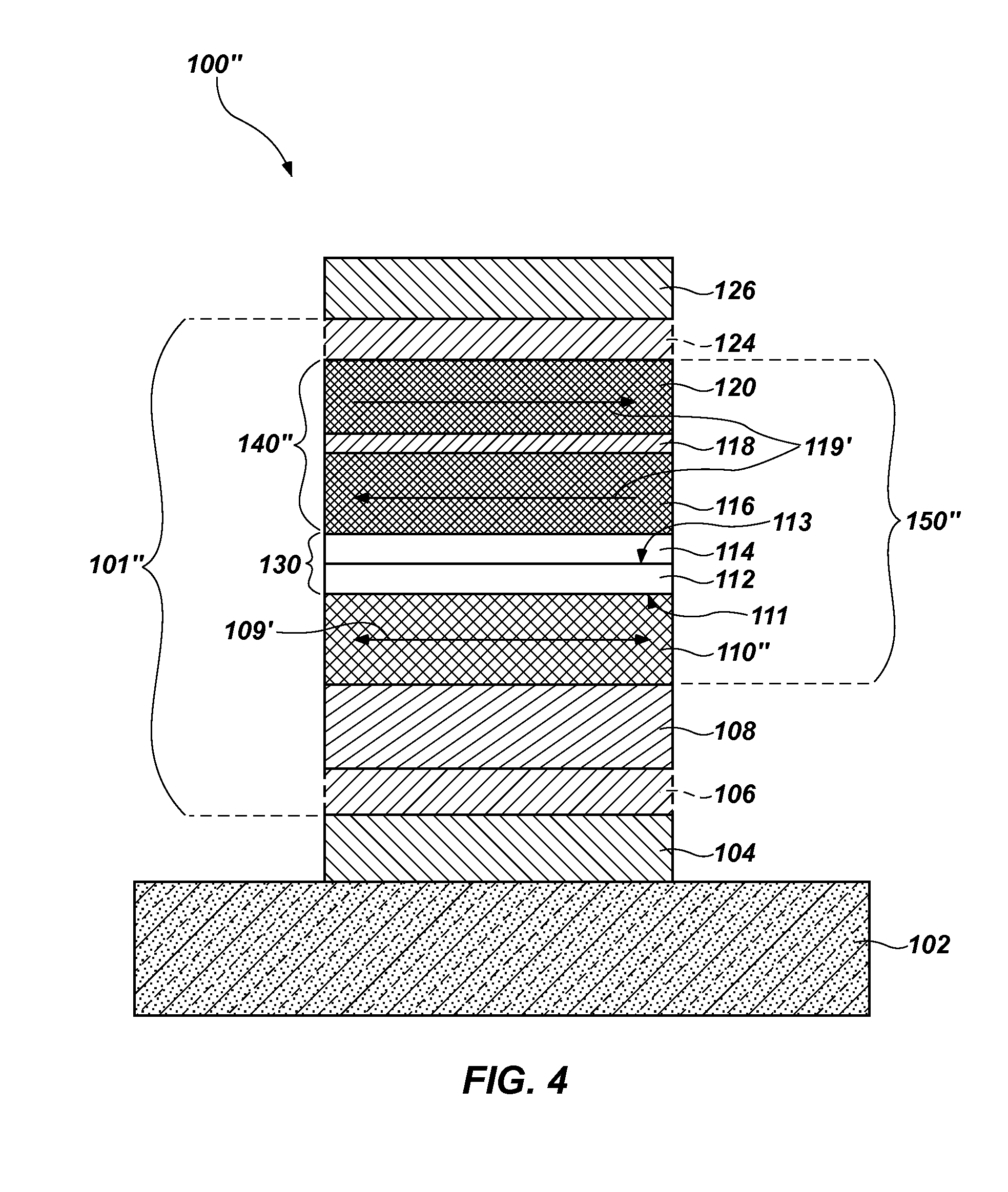
Referring to FIG. 1, a magnetic memory cell 100 including a magnetic cell core 101 according to some embodiments is illustrated. The magnetic cell core 101 may include a magnetic tunnel junction 150 and may be disposed between a lower electrode 104 and an upper electrode 126 over a substrate 102. The MTJ 150 may include a magnetic region and another magnetic region, for example, a "free region 110" and a "fixed region" 140, respectively. A tunnel barrier material 130 may be disposed between the free region 110 and the fixed region 140.
The substrate 102 may include a base material or other construction upon which components, such as those within memory cells, are formed. The substrate 102 may be a semiconductor substrate, a base semiconductor material on a supporting substrate, a metal electrode, or a semiconductor substrate having one or more materials, structures, or regions formed thereon. The substrate 102 may be a conventional silicon substrate or other bulk substrate including semiconductor material. As used herein, the term "bulk substrate" means and includes not only silicon wafers, but also silicon-on-insulator ("SOI") substrates, such as silicon-on-sapphire ("SOS") substrates or silicon-on-glass ("SOG") substrates, epitaxial layers of silicon on a base semiconductor foundation, or other semiconductor or optoelectronic materials, such as silicon-germanium (Si.sub.1-xGe.sub.x, where x is, for example, a mole fraction between 0.2 and 0.8), germanium (Ge), gallium arsenide (GaAs), gallium nitride (GaN), or indium phosphide (InP), among others. Furthermore, when reference is made to a "substrate" in the following description, previous process stages may have been utilized to form materials, regions, or junctions in the base semiconductor structure or foundation.
The lower electrode 104 may overlie the substrate 102. The lower electrode 104 may include a metal such as copper, tungsten, platinum, palladium, titanium, tantalum, nickel, titanium nitride (TiN), tantalum nitride (TaN), tungsten nitride (WN), polysilicon, a metal silicide, a metal alloy, or combinations thereof.
One or more lower intermediary regions 106 may, optionally, be disposed under the magnetic regions (e.g., the free region 110 and the fixed region 140). The lower intermediary region 106, if included, may be configured to inhibit diffusion of species between the lower electrode 104 and materials overlying the lower electrode 104. The lower intermediary region 106 may include a conductive material such as one or more of copper, tantalum, titanium, tungsten, ruthenium, tantalum nitride, and titanium nitride.
A seed material 108 may overlie the lower intermediary region 106, if present, or the lower electrode 104 if the lower intermediary region 106 is not present. The seed material 108 may include tantalum, platinum, ruthenium, iron, nickel, cobalt, chromium, titanium, zirconium, vanadium, copper, zinc, rhodium, silver, hafnium, tungsten, iridium, tantalum nitride, and combinations thereof. By way of non-limiting example, the seed material 108 may include tungsten and at least one of iron, cobalt, nickel, or another suitable material. In other embodiments, the seed material 108 may include iron and cobalt and may further include at least one transition element, such as tantalum, platinum, ruthenium, nickel, chromium, titanium, zirconium, vanadium, copper, zinc, rhodium, silver, hafnium, and tungsten. In yet other embodiments, the seed material 108 may include at least one of hafnium, zirconium, and tantalum and at least one of iron, cobalt, and nickel, such as FeHf. The seed material 108 may be a homogeneous composition of the seed material 108 or may include distinct portions of one or more of tantalum, platinum, ruthenium, iron, nickel, cobalt, chromium, titanium, zirconium, vanadium, copper, zinc, rhodium, silver, hafnium, tungsten, and iridium adjacent to a distinct portion of another of tantalum, platinum, ruthenium, iron, nickel, cobalt, chromium, titanium, zirconium, vanadium, copper, zinc, rhodium, silver, hafnium, tungsten, and iridium.
The free region 110 may overlie the seed material 108. In some embodiments, the free region 110 directly overlies and contacts the seed material 108. The free region 110 may include a magnetic material exhibiting a switchable magnetic orientation, indicated by arrows 109, during use and operation of the magnetic memory cell 100. The switchable magnetic orientation may be switched between a parallel configuration and an anti-parallel configuration by the application of a current or applied field to the magnetic memory cell 100.
In some embodiments, the free region 110 may be a conventional free region. In other embodiments, the free region 110 may include alternating portions of a magnetic material and a conductive material. However, the free region 110 is not so limited and may include other suitable magnetic materials that exhibit a switchable magnetic orientation.
In some embodiments, the free region 110 may include a ferromagnetic material including at least one of cobalt (Co) and iron (Fe) (e.g., Co.sub.xFe.sub.y, wherein x=10 to 80 and y=10 to 80) and, in some embodiments, also boron (B) (e.g., Co.sub.xFe.sub.yB.sub.z, wherein x=10 to 80, y=10 to 80, and z=0 to 50). Thus, the free region 110 may include at least one of Co, Fe, and B (e.g., a CoFeB material, a CoFe material, a FeB material, a CoB material, etc.). As used herein, the term "CoFeB material" means and includes a material comprising cobalt, iron, and boron (e.g., Co.sub.xFe.sub.yB.sub.z, wherein x=10 to 80, y=10 to 80, and z=0 to 50). A CoFeB material may or may not exhibit magnetism, depending on its configuration (e.g., its thickness). In other embodiments, the free region 110 may alternatively or additionally include nickel (Ni) (e.g., an NiB material). In some embodiments, the free region 110 may be substantially free of boron and may include, for example, CoFe. The CoFe may be formed as CoFeB and the boron may be diffused out of the free region 110 after formation thereof, or the CoFe may be formed (e.g., deposited) as CoFe, without any boron.
The free region 110 may be homogeneous, or may include one or more sub-regions (e.g., a CoFeB material, with sub-regions having different relative atomic ratios of Co, Fe, and B).
A tunnel barrier material 130 may overlie the free region 110. In some embodiments, the tunnel barrier material 130 directly overlies and contacts the free region 110. The tunnel barrier material 130 may include a nonmagnetic, crystalline material, such as magnesium oxide (MgO), aluminum oxide (Al.sub.2O.sub.3), titanium dioxide (TiO.sub.2), tantalum oxide (Ta.sub.2O.sub.5), ruthenium oxide (RuO.sub.2), boron oxide (B.sub.2O.sub.3), or combinations thereof. The tunnel barrier material 130 may be configured to induce interfacial magnetic anisotropy in the free region 110 and the fixed region 140 and may also be configured to function as a tunnel region of the MTJ 150 effected by interaction of the free region 110, the tunnel barrier material 130, and the fixed region 140.
The tunnel barrier material 130 may include a first portion 112 and a second portion 114. The first portion 112 may overlie the free region 110. In some embodiments, the first portion 112 directly overlies and contacts the free region 110. The first portion 112 may be formed over the free region 110 to form an interface 111 between the free region 110 and the tunnel barrier material 130. A crystal orientation of the MTJ 150 may not change at the interface 111 between the first portion 112 and the free region 110. By way of example and not limitation, each of the free region 110 and the first portion 112 may exhibit a bcc (001) crystal structure. As described in more detail below, each of the first portion 112 and the free region 110 may be amorphous (e.g., not crystalline) as formed, with the desired crystal structure occurring following an anneal. In some embodiments, the first portion 112 is an oxide material and may include MgO, Al.sub.2O.sub.3, TiO.sub.2, Ta.sub.2O.sub.5, RuO.sub.2, B.sub.2O.sub.3, or combinations thereof.
The second portion 114 may overlie the first portion 112. In some embodiments, the second portion 114 directly overlies and contacts the first portion 112. An interface 113 between the first portion 112 and the second portion 114 may be smooth and exhibit the same crystal orientation as the first portion 112 and the free region 110 (e.g., a bcc (001) crystal structure). The second portion 114 may be an oxide material and may include MgO, Al.sub.2O.sub.3, TiO.sub.2, Ta.sub.2O.sub.5, RuO.sub.2, B.sub.2O.sub.3, or combinations thereof. The first portion 112 and the second portion 114 may include the same material. In some embodiments, the first portion 112 and the second portion 114 include MgO. In some such embodiments, the second portion 114 includes a ratio of oxygen to magnesium closer to stoichiometric (e.g., 1:1) than the first portion 112. Thus, the second portion 114 may have less oxygen vacancies and less interstitial oxygen and also a higher density than the first portion 112. The second portion 114 may exhibit less structural defects than the first portion 112 and, in some embodiments, may exhibit a higher TMR and a lower RA than the first portion 112.
The tunnel barrier material 130 may have a total thickness (i.e., a sum of a thickness of the first portion 112 and a thickness of the second portion 114) of between about 10 .ANG. and about 30 .ANG., such as between about 10 .ANG. and about 15 .ANG., between about 15 .ANG. and about 20 .ANG., between about 20 .ANG. and about 25 .ANG., or between about 25 .ANG. and about 30 .ANG.. The tunnel barrier material 130 may have a thickness of between about 10 .ANG. and about 20 .ANG.. In some embodiments, the thickness of the tunnel barrier material 130 is about 18 .ANG..
The first portion 112 and the second portion 114 may have the same thickness, the first portion 112 may have a greater thickness than the second portion 114, or the second portion 114 may have a greater thickness than the first portion 112. The RA and the TMR of the MTJ 150 may be tailored by altering the thickness of the first portion 112 relative to the thickness of the second portion 114 of the tunnel barrier material 130. A ratio of the thickness of the first portion 112 to the thickness of the second portion 114 may be between about 0.9 and about 2.0, such as between about 0.9 and about 1.0, between about 1.0 and about 1.25, between about 1.25 and about 1.5, between about 1.2 and about 1.8, or between about 1.5 and about 2.0. In some embodiments, the ratio is between about 1.0 and about 1.5 and the total thickness of the tunnel barrier material 130 is about 18 .ANG..
The tunnel barrier material 130 having the first portion 112 and the second portion 114 may exhibit a TMR of between about 180% and about 600%, such as between about 180% and about 200%, between about 180% and about 225%, between about 180% and about 300%, between about 200% and about 220%, between about 220% and about 250%, between about 250% and about 300%, between about 300% and about 400%, or between about 400% and about 600%. In some embodiments, the TMR is between about 180% and about 300%. The tunnel barrier material 130 may exhibit a RA of between about 3 ohm .mu.m.sup.2 and about 8 ohm .mu.m.sup.2, such as between about 3 ohm .mu.m.sup.2 and about 4 ohm .mu.m.sup.2, between about 4 ohm .mu.m.sup.2 and about 5 ohm .mu.m.sup.2, between about 5 ohm .mu.m.sup.2 and about 6 ohm .mu.m.sup.2, between about 6 ohm .mu.m.sup.2 and about 7 ohm .mu.m.sup.2, or between about 7 ohm .mu.m.sup.2 and about 8 ohm .mu.m.sup.2. In some embodiments, the RA is between about 6 ohm .mu.m.sup.2 and about 7 ohm .mu.m.sup.2. In other embodiments, the tunnel barrier material 130 exhibits an RA of between about 4 ohm .mu.m.sup.2 and about 8 ohm .mu.m.sup.2 and a TMR of between about 180% and about 205%. By way of non-limiting example, the tunnel barrier material 130 may exhibit a RA of about 4 ohm .mu.m.sup.2 and a TMR of about 180%, or a RA of about 8 ohm .mu.m.sup.2 and a TMR of about 205% at a thickness of between about 10 .ANG. and about 20 .ANG..
The fixed region 140 may overlie the tunnel barrier material 130. In some embodiments, the fixed region 140 directly overlies and contacts the second portion 114 of the tunnel barrier material 130.
The fixed region 140 may include one or more magnetic materials and, optionally, one or more non-magnetic materials. For example, the fixed region 140 may be configured as a synthetic antiferromagnet including a sub-region of ruthenium or tantalum adjoined by magnetic sub-regions. The magnetic sub-regions may include a material including cobalt, and at least one of palladium and platinum, and combinations thereof, a CoFeB material, and combinations thereof. Alternatively, the fixed region 140 may be configured with structures of alternating sub-regions of magnetic material and coupler material. Each of the magnetic sub-regions may include one or more materials and one or more regions therein. As another example, the fixed region 140 may be configured as a single, homogeneous magnetic material. Accordingly, the fixed region 140 may have uniform magnetization, or sub-regions of differing magnetization that, overall, effect the fixed region 140 having a fixed magnetic orientation during use and operation of the magnetic memory cell 100.
The fixed region 140 may include a first magnetic portion 116 over the second portion 114 of the tunnel barrier material 130, a coupling material 118 over the first magnetic portion 116, and a second magnetic portion 120 over the coupling material 118. In some embodiments, the first magnetic portion 116 includes a first magnetic sub-region 116a that may include a CoFeB material overlying the second portion 114, a spacer 116b that may include a tantalum material overlying the first magnetic portion 116, and a second magnetic sub-region 116c that may include a material including cobalt and at least one of palladium and platinum (e.g., CoPd, CoPt) over the spacer 116b. The coupling material 118 may include a ruthenium material overlying the second magnetic sub-region 116c of the first magnetic portion 116. The second magnetic portion 120 may include a material including cobalt, palladium, platinum, and combinations thereof, such as cobalt and at least one of palladium and platinum. In some embodiments, the second magnetic portion 120 includes the same material as the second magnetic sub-region 116c of the first magnetic portion 116.
In other embodiments, the first magnetic portion 116 includes an artificial superlattice structure and the second magnetic portion 120 includes another artificial superlattice structure overlying the coupling material 118. Referring to FIG. 2, the artificial superlattice structure of the first magnetic portion 116 may include alternating portions of a magnetic material 117 and a conductive material 115. The conductive material 115 may enable the magnetic material 117 to exhibit a perpendicular anisotropy (i.e., a vertical magnetic orientation). The magnetic material 117 may include cobalt, iron, and combinations thereof. The conductive material 115 may include at least one of platinum, palladium, nickel, and iridium. In some embodiments, the magnetic material 117 includes cobalt and the conductive material 115 includes platinum. Although FIG. 2 depicts six regions of magnetic material 117 and six regions of conductive material 115 in the first magnetic portion 116, the artificial superlattice structure of the first magnetic portion 116 is not so limited and may include any number (e.g., one, two, three, four, five, etc.) of alternating regions of magnetic material 117 and conductive material 115.
In some embodiments, a region of the conductive material 115 of the first magnetic portion 116 may directly overlie and contact the second portion 114 of the tunnel barrier material 130. For example, a region of the conductive material 115 may directly overlie and contact the second portion 114 of the tunnel barrier material 130. In other embodiments, a region of the magnetic material 117 may directly overlie and contact the second portion 114 of the tunnel barrier material 130.
Referring back to FIG. 1, the coupling material 118 may overlie the first magnetic portion 116. In some embodiments, the coupling material 118 directly overlies and contacts the first magnetic portion 116 (e.g., the second magnetic sub-region 116c of the first magnetic portion 116). The coupling material 118 may include tantalum, ruthenium, rhodium, and combinations thereof. In some embodiments, the coupling material 118 is ruthenium. The coupling material 118 may have a thickness between about 1 .ANG. and about 10 .ANG.. In some embodiments, the coupling material 118 has a thickness between about 4 .ANG. and about 5 .ANG..
The second magnetic portion 120 may directly overlie the coupling material 118. The second magnetic portion 120 may include the same materials and may be substantially the same as at least a portion of the first magnetic portion 116. In some embodiments, the second magnetic portion 120 includes a material including cobalt and at least one of palladium and platinum and may include the same material as the second magnetic sub-region 116c of the first magnetic portion 116.
The first magnetic portion 116 and the second magnetic portion 120 of the fixed region 140 may include a fixed magnetic orientation, indicated by arrows 119. The fixed magnetic orientation may be north, south, east, west, etc. The fixed magnetic orientation of the first magnetic portion 116 and the second magnetic portion 120 may be the same or may be different.
One or more upper intermediary regions 124 may, optionally, be disposed over the fixed region 140. The upper intermediary region 124, if included, may be configured to inhibit diffusion of species between the upper electrode 126 and underlying materials during operation of the memory cell. The upper intermediary region 124 may include a conductive material (e.g., one or more materials such as copper, tantalum, titanium, tungsten, ruthenium, tantalum nitride, titanium nitride) that may form a conductive capping region.
The upper electrode 126 may overlie the upper intermediary region 124. The upper electrode 126 may include copper, tungsten, platinum, palladium, titanium, tantalum, nickel, titanium nitride, tantalum nitride, tungsten nitride, polysilicon, a metal silicide, a metal alloy, or combinations thereof. In some embodiments, the upper electrode 126 includes the same materials as the lower electrode 104.
The magnetic memory cell 100 of FIG. 1 is configured as a "top pinned" memory cell (i.e., a memory cell in which the fixed region 140 is disposed over the free region 110). However, in other embodiments, such as that of FIG. 3, a free region 110' may overlie a fixed region 140'. Thus, with reference to FIG. 3, a magnetic memory cell 100' including a MTJ 150' may be configured as a "bottom pinned" memory cell. The magnetic memory cell 100' may include a magnetic cell core 101' disposed between the lower electrode 104 and the upper electrode 126.
The magnetic memory cell 100' may include a lower intermediary region 106 overlying the lower electrode 104. The seed material 108 may overlie the lower intermediary region 106, if present. In other embodiments, the seed material 108 may directly overlie and contact the lower electrode 104. The seed material 108 may be the same as described above with reference to FIG. 1.
The fixed region 140' may directly overlie and contact the seed material 108. The fixed region 140' may include a fixed magnetic orientation, indicated by arrows 119. The fixed region 140' may include the same materials described above with reference to fixed region 140. In some embodiments, the fixed region 140' includes a second magnetic portion 120', a coupling material 118', and a first magnetic portion 116'. The first magnetic portion 116' may include a first magnetic sub-region 116a', a spacer 116b', and a second magnetic sub-region 116c'. The first magnetic sub-region 116a', the spacer 116b', and the second magnetic sub-region 116c' may be the same as the first magnetic sub-region 116a, the spacer 116b, and the second magnetic sub-region 116c, respectively, described above with reference to FIG. 1. Each of the first magnetic portion 116', the coupling material 118', and the second magnetic portion 120' may be the same as the first magnetic portion 116, the coupling material 118, and the second magnetic portion 120, respectively, described above with reference to FIG. 1. However, the fixed region 140' may not directly overlie the tunnel barrier material 130 as in the magnetic memory cell 100 of FIG. 1. Rather, the second magnetic portion 120' of the fixed region 140' may directly overlie and contact the underlying seed material 108. The coupling material 118' may overlie the second magnetic portion 120' and the first magnetic portion 116' may overlie the coupling material 118'.
The tunnel barrier material 130 may overlie the fixed region 140'. The first portion 112 of the tunnel barrier material 130 may directly overlie and contact the fixed region 140'. The first portion 112 may be formed over the fixed region 140' to form an interface 111' between the fixed region 140' and the tunnel barrier material 130. The fixed region 140' may exhibit a crystal structure that is aligned with a crystal structure of the first portion 112. By way of example and not limitation, each of the first portion 112 and the fixed region 140' may exhibit a bcc (001) crystal structure without a change in the crystal structure of the MTJ 150' at the interface 111'.
The tunnel barrier material 130 may include the same materials as described above with reference to FIG. 1. Thus, each of the first portion 112 and the second portion 114 of the tunnel barrier material 130 may be the same as described above with reference to FIG. 1. An interface 113' between the first portion 112 and the second portion 114 may be smooth and exhibit the same crystal orientation as the interface 111' on which the first portion 112 is formed. The tunnel barrier material 130 may be disposed directly between the fixed region 140' and the free region 110'.
The free region 110' may directly overlie and contact the tunnel barrier material 130. In some embodiments, the free region 110' directly overlies and contacts the second portion 114 of the tunnel barrier material 130. The free region 110' may include the same materials as described above with reference to FIG. 1. The free region 110' may include a switchable magnetic orientation, indicated by arrows 109.
The optional upper intermediary region 124 may overlie the free region 110'. The upper electrode 126 may overlie the upper intermediary region 124, if present.
The memory cells of embodiments of the disclosure may be configured as "out-of-plane" STT-MRAM cells. "Out-of-plane" STT-MRAM cells may include magnetic regions exhibiting a magnetic orientation that is predominately oriented in a vertical direction (e.g., a direction that is perpendicular to a width and length of the respective region or a direction that is perpendicular to a primary surface of the substrate on which the STT-MRAM cell is located). For example, as illustrated in FIG. 1 and FIG. 3, an STT-MRAM cell (e.g., magnetic memory cell 100, magnetic memory cell 100') may be configured to exhibit a vertical magnetic orientation in at least one of the magnetic regions (e.g., the free region 110, 110' and the fixed region 140, 140'). As indicated in FIG. 1 and FIG. 3, each of the free region 110, 110' and the fixed region 140, 140' may exhibit a vertical magnetic orientation as indicated by the arrows 109 and the arrows 119. The magnetic orientation of the fixed region 140, 140' may remain directed in essentially the same direction throughout use and operation of the STT-MRAM cell, for example, in the direction indicated by arrows 119. The magnetic orientation of the free region 110, 110', on the other hand, may be switched during use and operation of the cell, between a parallel configuration and an anti-parallel configuration, as indicated by the arrows 109. As another example, as illustrated in FIG. 4, an in-plane magnetic memory cell 100'' including a magnetic cell core 101'' may be configured to exhibit a horizontal magnetic orientation in at least one of the magnetic regions (e.g., a free region 110'' and a fixed region 140'') of an MTJ 150'', as indicated by arrow 109' in the free region 110'' and arrow 119' in the fixed region 140''.
A semiconductor device may include at least one magnetic memory cell including the magnetic cell cores 101, 101', 101'' of the disclosure disposed between a pair of electrodes.
Accordingly, a semiconductor device is disclosed. The semiconductor device comprises a magnetic tunnel junction over a seed material on a substrate, the magnetic tunnel junction exhibiting a tunnel magnetoresistance of between about 180% and about 300% and comprising a magnetic material over the seed material, an oxide material over the magnetic material, another oxide material over the oxide material, the oxide material and the another oxide material having a thickness of between about 10 .ANG. and about 20 .ANG., and another magnetic material over the another oxide material.
Referring to FIG. 5A through FIG. 5C, a method of forming the magnetic memory cell 100 of FIG. 1 is shown. The method may include forming a magnetic memory cell 200 over a substrate 202. A lower electrode material 204 may be formed over the substrate 202. The lower electrode material may include any of the materials described above with reference to the lower electrode 104.
An intermediary region material 206 may, optionally, be formed over the lower electrode material 204. The lower intermediary region material 206 may be formed from any of the materials described above with reference to the lower intermediary region 106. In some embodiments, the lower intermediary region material 206 may be integral with the conductive material of the lower electrode material 204. For example, the lower intermediary region material 206 may be an upper-most sub-region of the lower electrode material 204.
A seed material 208 may be formed over the lower intermediary region material 206, if present, or the lower electrode material 204. The seed material 208 may be formed as described above with reference to FIG. 1. Each portion of the seed material 208 may be formed by sputter deposition, such as by magnetron sputtering (e.g., high-power impulse magnetron sputtering (HIPIMS), dc magnetron sputtering, etc.), ion-beam sputtering, or other PVD methods. The seed material 208 may be also formed by at least one of atomic layer deposition (ALD), chemical vapor deposition (CVD), plasma enhanced chemical vapor deposition (PECVD), low pressure chemical vapor deposition (LPCVD), or other film deposition processes.
A free region material 210 may be formed over the seed material 208. The free region material 210 may be formed of any of the materials described above with reference to the free region 110. For example, the free region material 210 may include a CoFeB material. In other embodiments, the free region material 210 may include an artificial superlattice structure material formed of alternating portions of the magnetic material 117 and the conductive material 115, as described above with reference to the first magnetic portion 116 of FIG. 2. The free region material 210 may be amorphous when formed and may be formed at a temperature such that the free region material 210 remains in an amorphous state. The free region material 210 may exhibit a switchable magnetic orientation, indicated by arrows 209.
As shown in FIGS. 5A and 5B, a tunnel barrier material 230 may be formed over the free region material 210. The tunnel barrier material 230 may include a first portion 212 and a second portion 214. The first portion 212 of the tunnel barrier material 230 may be formed over the free region material 210 to form an interface 211. The first portion 212 of the tunnel barrier material 230 may be formed from the same materials as described above with reference to the first portion 112 of the tunnel barrier material 130.
The first portion 212 may be formed by at least one of ALD, CVD, PECVD, LPCVD, PVD, or other film deposition processes. In some embodiments, the first portion 212 is formed by sputter deposition, such as by magnetron sputtering (e.g., high-power impulse magnetron sputtering (HIPIMS), DC sputtering, etc.), RF sputtering, electron beam physical vapor deposition, ion-beam reactive sputtering, or other PVD methods. In some embodiments, the first portion 212 is formed from MgO. The first portion 212 may be formed as MgO, rather than formed as a magnesium portion that is subsequently oxidized to MgO by exposing the magnesium portion to oxidizing conditions. The source of the MgO may be a single crystal MgO or a multi-crystal MgO deposition source or sputtering target.
The first portion 212 may be formed over the free region material 210 at a first temperature such that the underlying free region material 210 is not crystallized. In other words, the free region material 210 may remain amorphous during formation of the first portion 212 of the tunnel barrier material 230. As formed, the first portion 212 may be amorphous or crystalline. In some embodiments, the free region material 210 includes a CoFeB material that remains amorphous during formation of the first portion 212. In some embodiments, the first portion 212 is crystalline when initially formed. The first portion 212 may be formed at a temperature between about -150.degree. C. and about 150.degree. C., such as between about -150.degree. C. and about 0.degree. C., between about 0.degree. C. and about 25.degree. C., between about 20.degree. C. and about 25.degree. C., between about 25.degree. C. and about 50.degree. C., or between about 50.degree. C. and about 150.degree. C. In some embodiments, the first portion 212 is formed at room temperature (e.g., between about 20.degree. C. and about 25.degree. C.). If the first portion 212 is formed at room temperature, the underlying free region material 210 may remain in its amorphous state.
After forming the first portion 212 of the tunnel barrier material 230 over the free region material 210, the free region material 210 and the first portion 212 may be annealed, such as by thermal annealing. Exposing the free region material 210 and the first portion 212 to annealing conditions may crystallize the free region material 210 from the interface 211 through the free region material 210. After annealing the first portion 212 and the free region material 210, the free region material 210 may have a crystal structure that is aligned with (i.e., matched to) a crystal structure of the first portion 212. In some embodiments, a CoFeB free region material 210 is crystallized from the interface 211 and includes the same crystal structure as the first portion 212 including MgO. Annealing the first portion 212 may also cause any oxygen vacancies within the first portion 212 to fill with oxygen, increasing the stoichiometry of the first portion 212 of the tunnel barrier material 230. By way of non-limiting example, where the first portion 212 includes MgO, annealing the first portion 212 may attract oxygen to the first portion 212, filling any oxygen vacancies that may have been formed during the low temperature formation of the first portion 212.
To anneal the free region material 210 and the first portion 212, the free region material 210 and the first portion 212 may be exposed to a temperature sufficient to crystallize the free region material 210 and for a sufficient amount of time. Exposing the first portion 212 to annealing conditions may increase the crystal quality of the first portion 212 upon which the second portion 214 may be subsequently formed, as described in more detail below. The annealing may also form a smooth surface of the first portion 212, upon which the second portion 214 is formed. The free region material 210 and the first portion 212 may be exposed to a temperature of between about 300.degree. C. and about 600.degree. C. for between about 60 seconds and about one hour (1 hr.). The free region material 210 and the first portion 212 may be exposed to a temperature of between about 300.degree. C. and about 350.degree. C., between about 350.degree. C. and about 400.degree. C., between about 400.degree. C. and about 500.degree. C., or between about 500.degree. C. and about 600.degree. C. The exposure time may be between about 60 seconds and about five minutes, between about 5 minutes and 15 minutes, between about 15 minutes and about 30 minutes, or between about 30 minutes and about 60 minutes.
Referring to FIG. 5B, after annealing the free region material 210 and the first portion 212, the second portion 214 of the tunnel barrier material 230 may be formed. The second portion 214 may be formed directly over and in contact with the first portion 212. The second portion may be formed of the same materials described above with reference to the second portion 114. In some embodiments, the second portion 214 is formed of the same material as the first portion 212. The first portion 212 of the tunnel barrier material 230 that has been annealed may act as a seed upon which the second portion 214 is formed, such that the crystal structure of the second portion 214 matches the crystal structure of the first portion 212. An exposed surface of the first portion 212 may be a seed upon which the second portion 214 is formed to the same crystal orientation as the first portion 212 and the free region material 210. The first portion 212 and the second portion 214 may exhibit the same crystal orientation at an interface 213.
The second portion 214 of the tunnel barrier material 230 may be formed at a second temperature that is higher than the first temperature at which the first portion 212 is formed. The second portion 214 may be formed by one of the same methods described above for forming the first portion 212. For example, the second portion 214 may be formed by sputter deposition, such as by at least one of ALD, CVD, PECVD, LPCVD, PVD, or other film deposition processes. In some embodiments, the second portion 214 is formed by sputter deposition, such as by magnetron sputtering (e.g., high-power impulse magnetron sputtering (HIPIMS), DC sputtering, etc.), RF sputtering, electron beam physical vapor deposition, ion-beam reactive sputtering, or other PVD methods. However, the second portion 214 may be formed at a different, higher temperature than the first portion 212 is formed. For example, the second portion 214 may be formed at a temperature between about 300.degree. C. and about 600.degree. C., as described above. The second portion 214 may be formed at the same temperature as the temperature at which the first portion 212 and the free region material 210 are annealed. In other embodiments, the second portion 214 may be formed at a different temperature than the temperature at which the first portion 212 and the free region material 210 are annealed. By way of non-limiting example, the second portion 214 may be formed at a temperature between about 300.degree. C. and about 600.degree. C., such as between about 300.degree. C. and about 350.degree. C., between about 350.degree. C. and about 400.degree. C., between about 400.degree. C. and about 500.degree. C., or between about 500.degree. C. and about 600.degree. C. Forming the second portion 214 at an elevated temperature may form a more stoichiometric material having an increased crystal quality. For example, where the second portion 214 includes MgO, the second portion 214 may include a stoichiometric amount of oxygen with less oxygen vacancies and less interstitial oxygen than the first portion 212. In some embodiments, each of the first portion 212 and the second portion 214 have a ratio of magnesium to oxygen of approximately one to one.
The second portion 214 may be formed to the same thickness, a greater thickness, or a lesser thickness than the first portion 212. In some embodiments, the ratio is about 1.5 and the total thickness of the tunnel barrier material 130 is about 18 .ANG.. The ratio of the thickness of the first portion 212 to the second portion 214 may be tailored to increase the TMR and decrease the RA of the tunnel barrier material 230. The tunnel barrier material 230 may be formed to exhibit a TMR of between about 180% and about 600% and an RA of between about 3 ohm .mu.m.sup.2 and about 8 ohm .mu.m.sup.2, as described above with reference to the tunnel barrier material 130. In some embodiments, the thickness of the second portion 214 is less than a thickness of the first portion 212.
With reference to FIG. 5C, a fixed region material 240 may be formed over the second portion 214 of the tunnel barrier material 230. The fixed region material 240 may include a first magnetic material 216 over the second portion 214 of the tunnel barrier material 230, a coupling material 218 over the first magnetic material 216, and a second magnetic material 220 over the coupling material 218. The first magnetic material 216 may include a first magnetic sub-region 216a, a spacer material 216b, and a second magnetic sub-region 216c. Each of the first magnetic sub-region 216a, the spacer material 216b, and the second magnetic sub-region 216c may be formed of the same materials as the first magnetic sub-region 116a, the spacer 116b, and the second magnetic sub-region 116c, respectively, described above. Each of the first magnetic material 216, the coupling material 218, and the second magnetic material 220 may be formed of the same materials as the first magnetic portion 116, the coupling material 118, and the second magnetic portion 120, respectively, described above. The first magnetic material 216 and the second magnetic material 220 of the fixed region material 240 may include a fixed magnetic orientation, indicated by arrows 219.
The coupling material 218 may be formed over the first magnetic material 216 (e.g., over the second magnetic sub-region 216c of the first magnetic material 216). The coupling material 218 may be formed between the first magnetic material 216 and the second magnetic material 220. The coupling material 218 may be formed by at least one of ALD, CVD, PVD, PECVD, LPCVD, or other film deposition processes.
The second magnetic material 220 may be formed directly over the coupling material 218. The second magnetic material 220 may be formed in the same manner and from the same materials as the first magnetic material 216.
An upper intermediary region material 224 may optionally be formed over the second magnetic material 220 and may include the same materials as the lower intermediary region material 206. An upper electrode material 226 may be formed over the upper intermediary region material 224, if present, or over the second magnetic material 220. The upper electrode material 226 may be formed of the same materials as described above with reference to the upper electrode 126.
The magnetic memory cell 200 may be processed to form the magnetic memory cell 100 as shown in FIG. 1. The magnetic memory cell 200 structure may be processed by conventional photolithography, material removal, etching, or other processes that are not described in detail herein.
Although the magnetic memory cell 200 described with reference to FIG. 5A through FIG. 5C describes forming the magnetic memory cell 100 of FIG. 1, the magnetic memory cell 100' of FIG. 3 may be formed by similar methods. However, the fixed region material 240 would be formed over the seed material 208, the first portion 212 of the tunnel barrier material 230 would be formed over the fixed region material 240, and the free region material 210 would be formed over the second portion 214 of the tunnel barrier material 230, resulting in the magnetic memory cell of FIG. 3. In other embodiments, the magnetic memory cell 100'' of FIG. 4 may be formed by forming the free region material 210 and the fixed region material 240 to exhibit a horizontal magnetic orientation.
Forming the tunnel barrier material 230 from the first portion 212 and the second portion 214 may increase the TMR and decrease the RA of the magnetic tunnel junction. The MTJ 150 may be substantially free of defects such as oxygen vacancies or interstitial oxygen within the crystal structure of the tunnel barrier material 230. The tunnel barrier material 230 may, therefore, exhibit improved tunneling characteristics at a high TMR and a low RA.
Accordingly, a method of forming a semiconductor device is disclosed. The method comprises forming a magnetic material over an electrode on a substrate, forming a first tunnel barrier material over the magnetic material, annealing the magnetic material and the first tunnel barrier material, forming a second tunnel barrier material over the annealed first tunnel barrier material, forming another magnetic material over the second tunnel barrier material, and forming another electrode over the another magnetic material.
Accordingly, a method of forming a magnetic tunnel junction is disclosed. The method comprises forming at a first temperature a barrier material over a magnetic material, annealing the barrier material and the magnetic material, forming at a second temperature another barrier material over the annealed barrier material, and forming another magnetic material over the another barrier material.
Accordingly, a method of forming a semiconductor device is disclosed. The method comprises forming a seed material over a substrate, forming a magnetic material over the seed material, forming at a first temperature an oxide material over the magnetic material, forming at a second temperature higher than the first temperature, another oxide material over the oxide material, and forming another magnetic material over the another oxide material.
With reference to FIG. 6, illustrated is an STT-MRAM system 600 that includes peripheral devices 612 in operable communication with an STT-MRAM cell 614, a grouping of which may be fabricated to form an array of memory cells in a grid pattern including a number of rows and columns, or in various other arrangements, depending on the system requirements and fabrication technology. The STT-MRAM cell 614 may include a magnetic cell core 601, an access transistor 603, a conductive material that may function as a data/sense line 604 (e.g., a bit line), a conductive material that may function as an access line 605 (e.g., a word line) and a conductive material that may function as a source line 606. The peripheral devices 612 of the STT-MRAM system may include read/write circuitry 607, a bit line reference 608, and a sense amplifier 609. The magnetic cell core 601 may be any one of the magnetic cell cores 101, 101', 101'' described above. Due to the structure of the magnetic cell core 601, the method of fabrication, or both, the STT-MRAM cell 614 may have a high TMR and a low resistance (e.g., low RA product).
In use and operation, when an STT-MRAM cell 614 is selected to be programmed, a programming current is applied to the STT-MRAM cell 614, and the current is spin-polarized by the fixed region of the magnetic cell core 601 and exerts a torque on the free region of the magnetic cell core 601, which switches the magnetization of the free region to "write to" or "program" the STT-MRAM cell 614. In a read operation of the STT-MRAM cell 614, a current is used to detect the resistance state of the magnetic cell core 601.
To initiate programming of the STT-MRAM cell 614, the read/write circuitry 607 may generate a write current (i.e., a programming current) to the data/sense line 604 and the source line 606. The polarity of the voltage between the data/sense line 604 and the source line 606 determines the switch in magnetic orientation of the free region in the magnetic cell core 601. By changing the magnetic orientation of the free region with the spin polarity, the free region is magnetized according to the spin polarity of the programming current and the programmed logic state is written to the STT-MRAM cell 614.
To read the STT-MRAM cell 614, the read/write circuitry 607 generates a read voltage to the data/sense line 604 and the source line 606 through the magnetic cell core 601 and the access transistor 603. The programmed state of the STT-MRAM cell 614 relates to the electrical resistance across the magnetic cell core 601, which may be determined by the voltage difference between the data/sense line 604 and the source line 606. In some embodiments, the voltage difference may be compared to the bit line reference 608 and amplified by the sense amplifier 609.
FIG. 6 illustrates one example of a STT-MRAM system 600 including at least one magnetic memory cell. It is contemplated, however, that the magnetic cell cores 101, 101', 101'' may be incorporated and utilized within any STT-MRAM system configured to incorporate a magnetic cell core having magnetic regions. It is also contemplated that the magnetic cell cores 101, 101', 101'' may be used in other magnetic memory cells besides STT-MRAM cells.
With reference to FIG. 7, illustrated is a simplified block diagram of a semiconductor device 700 implemented according to one or more embodiments described herein. The semiconductor device 700 includes a memory array 702 and a control logic component 704. The memory array 702 may include a plurality of STT-MRAM cells 614 (FIG. 6) including any of the magnetic cell cores (e.g., the magnetic cell cores 101, 101', 101'' of FIG. 1, FIG. 3, and FIG. 4, respectively) discussed above, which magnetic cell cores (e.g., the magnetic cell cores 101, 101', 101'') may have been formed according to a method described above and may be operated according to a method described above. The control logic component 704 may be configured to operatively interact with the memory array 702 so as to read from or write to any or all memory cells (e.g., STT-MRAM cell 614 (FIG. 6)) within the memory array 702.
Accordingly, a semiconductor device is disclosed. The semiconductor device comprises an array of magnetic cell structures, each magnetic cell structure comprising a magnetic tunnel junction over an electrode on a substrate, each magnetic tunnel junction comprising a magnetic material over the substrate, a first tunnel barrier material over the magnetic material, a second tunnel barrier material over the first tunnel barrier material, and another magnetic material over the second tunnel barrier material, each magnetic tunnel junction configured to exhibit a tunnel magnetoresistance of between about 180% and about 600% at a resistance area product of less than about 8 ohm .mu.m.sup.2. The semiconductor device further comprises another electrode over the another magnetic material.
With reference to FIG. 8, depicted is a processor-based system 800. The processor-based system 800 may include various electronic devices manufactured in accordance with embodiments of the present disclosure. The processor-based system 800 may be any of a variety of types such as a computer, pager, cellular phone, personal organizer, control circuit, or other electronic device. The processor-based system 800 may include one or more processors 802, such as a microprocessor, to control the processing of system functions and requests in the processor-based system 800. The processor 802 and other subcomponents of the processor-based system 800 may include magnetic memory devices manufactured in accordance with embodiments of the present disclosure.
The processor-based system 800 may include a power supply 804 in operable communication with the processor 802. For example, if the processor-based system 800 is a portable system, the power supply 804 may include one or more of a fuel cell, a power scavenging device, permanent batteries, replaceable batteries, and rechargeable batteries. The power supply 804 may also include an AC adapter; therefore, the processor-based system 800 may be plugged into a wall outlet, for example. The power supply 804 may also include a DC adapter such that the processor-based system 800 may be plugged into a vehicle cigarette lighter or a vehicle power port, for example.
Various other devices may be coupled to the processor 802 depending on the functions that the processor-based system 800 performs. For example, a user interface 806 may be coupled to the processor 802. The user interface 806 may include input devices such as buttons, switches, a keyboard, a light pen, a mouse, a digitizer and stylus, a touch screen, a voice recognition system, a microphone, or a combination thereof. A display 808 may also be coupled to the processor 802. The display 808 may include an LCD display, an SED display, a CRT display, a DLP display, a plasma display, an OLED display, an LED display, a three-dimensional projection, an audio display, or a combination thereof. Furthermore, an RF sub-system/baseband processor 810 may also be coupled to the processor 802. The RF sub-system/baseband processor 810 may include an antenna that is coupled to an RF receiver and to an RF transmitter (not shown). A communication port 812, or more than one communication port 812, may also be coupled to the processor 802. The communication port 812 may be adapted to be coupled to one or more peripheral devices 814, such as a modem, a printer, a computer, a scanner, or a camera, or to a network, such as a local area network, remote area network, intranet, or the Internet, for example.
The processor 802 may control the processor-based system 800 by implementing software programs stored in the memory. The software programs may include an operating system, database software, drafting software, word processing software, media editing software, or media playing software, for example. The memory is operably coupled to the processor 802 to store and facilitate execution of various programs. For example, the processor 802 may be coupled to system memory 816, which may include one or more of spin torque transfer magnetic random access memory (STT-MRAM), magnetic random access memory (MRAM), dynamic random access memory (DRAM), static random access memory (SRAM), racetrack memory, and other known memory types. The system memory 816 may include volatile memory, non-volatile memory, or a combination thereof. The system memory 816 is typically large so that it can store dynamically loaded applications and data. In some embodiments, the system memory 816 may include semiconductor devices, such as the semiconductor device 700 of FIG. 7, memory cells including any of the magnetic cell cores 101, 101', 101'' of FIG. 1, FIG. 3, and FIG. 4, respectively, described above, or a combination thereof.
The processor 802 may also be coupled to non-volatile memory 818, which is not to suggest that system memory 816 is necessarily volatile. The non-volatile memory 818 may include one or more of STT-MRAM, MRAM, read-only memory (ROM) such as an EPROM, resistive read-only memory (RROM), and flash memory to be used in conjunction with the system memory 816. The size of the non-volatile memory 818 is typically selected to be just large enough to store any necessary operating system, application programs, and fixed data. Additionally, the non-volatile memory 818 may include a high capacity memory such as disk drive memory, such as a hybrid-drive including resistive memory or other types of non-volatile solid-state memory, for example. The non-volatile memory 818 may include semiconductor devices, such as the semiconductor device 700 of FIG. 7, memory cells including any of the magnetic cell cores 101, 101', 101'' of FIG. 1, FIG. 3, and FIG. 4, respectively, or a combination thereof.
EXAMPLES
Example
FIG. 9 is a graphical representation comparing the TMR vs. the RA of MTJs formed according to embodiments of the disclosure to MTJs formed by conventional methods. A MgO tunnel barrier material was formed by RF sputtering at about 20.degree. C. over a CoFeB magnetic material. The MgO and the CoFeB were annealed at a temperature of about 500.degree. C. to crystallize the CoFeB magnetic material in the same crystal orientation as the MgO. A second MgO tunnel barrier material was formed by RF sputtering at about 500.degree. C. over the annealed MgO. Another CoFeB magnetic material was formed over the second MgO tunnel barrier material. A tantalum material was formed over the CoFeB magnetic material and a cobalt/palladium magnetic material was formed over the tantalum to complete the MTJ structure. A conventional MTJ was formed by forming an MgO tunnel barrier material over a CoFeB magnetic material at room temperature. The MgO and the CoFeB were annealed at a temperature of about 500.degree. C. Another CoFeB magnetic material was formed over the MgO. The TMR and the RA of the MTJ structures were measured using conventional techniques. The upper left line of FIG. 9 shows the TMR and the RA of MTJs formed according to embodiments of the disclosure and the lower right line shows the TMR and the RA of the MTJs formed by conventional methods. As shown in the graph, the MTJs formed by the methods disclosed herein exhibit a higher TMR at a lower RA than MTJs formed by conventional methods.
FIG. 10 is a graphical representation of the TMR vs. the RA of MTJs formed according to the present disclosure. A first MgO tunnel barrier material was formed to a first thickness ("X") over a CoFeB magnetic material. The MgO was formed by RF sputtering at about 20.degree. C. The MgO and the CoFeB were annealed at a temperature of about 500.degree. C. to crystallize the CoFeB in the same crystal orientation as the MgO. A second MgO tunnel barrier material was formed by RF sputtering at about 500.degree. C. over the annealed MgO. The second MgO tunnel barrier material was formed to a second thickness ("Y"). Another CoFeB magnetic material was formed over the second MgO tunnel barrier material. A tantalum material was formed over the CoFeB magnetic material and a cobalt/palladium magnetic material was formed over the tantalum to complete the MTJ structure. The TMR and RA of the MTJ structure were measured by conventional techniques. FIG. 10 graphs the TMR and the RA of MTJs having different ratios of the thickness of the first MgO tunnel barrier material to the thickness of the second MgO tunnel barrier material (i.e., X/Y). Accordingly, the ratio of X/Y may be tailored to form a MTJ exhibiting a desired TMR at a desired RA.
While certain illustrative embodiments have been described in connection with the figures, those of ordinary skill in the art will recognize and appreciate that embodiments encompassed by the disclosure are not limited to those embodiments explicitly shown and described herein. Rather, many additions, deletions, and modifications to the embodiments described herein may be made without departing from the scope of embodiments encompassed by the disclosure, such as those hereinafter claimed, including legal equivalents. In addition, features from one disclosed embodiment may be combined with features of another disclosed embodiment while still being encompassed within the scope of the disclosure.
* * * * *
References
D00000
D00001
D00002
D00003
D00004
D00005
D00006
D00007
D00008
XML
uspto.report is an independent third-party trademark research tool that is not affiliated, endorsed, or sponsored by the United States Patent and Trademark Office (USPTO) or any other governmental organization. The information provided by uspto.report is based on publicly available data at the time of writing and is intended for informational purposes only.
While we strive to provide accurate and up-to-date information, we do not guarantee the accuracy, completeness, reliability, or suitability of the information displayed on this site. The use of this site is at your own risk. Any reliance you place on such information is therefore strictly at your own risk.
All official trademark data, including owner information, should be verified by visiting the official USPTO website at www.uspto.gov. This site is not intended to replace professional legal advice and should not be used as a substitute for consulting with a legal professional who is knowledgeable about trademark law.