Thin-film transistor structure with three-dimensional fin-shape channel and preparation method thereof
Wang , et al. O
U.S. patent number 10,431,688 [Application Number 15/749,969] was granted by the patent office on 2019-10-01 for thin-film transistor structure with three-dimensional fin-shape channel and preparation method thereof. This patent grant is currently assigned to SUN YAT-SEN UNIVERSITY, SUN YAT-SEN UNIVERSITY CARNEGIE MELLON UNIVERSITY SHUNDE INTERNATIONAL JOINT RESEARCH INSTITUTE. The grantee listed for this patent is Sun Yat-Sen University, SUN YAT-SEN UNIVERSITY CARNEGIE MELLON UNIVERSITY SHUNDE INTERNATIONAL JOINT RESEARCH INSTITUTE. Invention is credited to Jun Chen, Hai Ou, Kai Wang.


| United States Patent | 10,431,688 |
| Wang , et al. | October 1, 2019 |
Thin-film transistor structure with three-dimensional fin-shape channel and preparation method thereof
Abstract
The present invention discloses a thin-film transistor structure with a three-dimensional fin-shape channel and a preparation method thereof. The preparation method includes following steps: (a) depositing and etching a bottom gate electrode on a substrate; (b) depositing a bottom dielectric layer at an upper part of a structure obtained from the step (a), and sequentially depositing a semiconductor film on the bottom dielectric layer; (c) etching the semiconductor film to obtain a fin-type channel; (d) respectively depositing an ohmic contact layer, a source electrode and a drain electrode on the semiconductor film located at both sides of the fin-shape channel, and etching; (e) depositing a top dielectric layer and a top gate electrode at an upper part of a structure obtained from the step (d); and (f) etching the top gate electrode, an completing a preparation of a thin-film transistor with a dual-gate three-dimensional fin-shape channel.
| Inventors: | Wang; Kai (Guangzhou, CN), Ou; Hai (Guangzhou, CN), Chen; Jun (Guangzhou, CN) | ||||||||||
|---|---|---|---|---|---|---|---|---|---|---|---|
| Applicant: |
|
||||||||||
| Assignee: | SUN YAT-SEN UNIVERSITY
(Guangdong, CN) SUN YAT-SEN UNIVERSITY CARNEGIE MELLON UNIVERSITY SHUNDE INTERNATIONAL JOINT RESEARCH INSTITUTE (Guangdong, CN) |
||||||||||
| Family ID: | 55101237 | ||||||||||
| Appl. No.: | 15/749,969 | ||||||||||
| Filed: | July 30, 2016 | ||||||||||
| PCT Filed: | July 30, 2016 | ||||||||||
| PCT No.: | PCT/CN2016/092450 | ||||||||||
| 371(c)(1),(2),(4) Date: | February 02, 2018 | ||||||||||
| PCT Pub. No.: | WO2017/020796 | ||||||||||
| PCT Pub. Date: | February 09, 2017 |
Prior Publication Data
| Document Identifier | Publication Date | |
|---|---|---|
| US 20180233599 A1 | Aug 16, 2018 | |
Foreign Application Priority Data
| Aug 4, 2015 [CN] | 2015 1 0472392 | |||
| Current U.S. Class: | 1/1 |
| Current CPC Class: | H01L 31/022408 (20130101); H01L 29/66 (20130101); H01L 29/7848 (20130101); H01L 29/66477 (20130101); H01L 29/78696 (20130101); H01L 29/78603 (20130101); H01L 29/78648 (20130101); H01L 29/78618 (20130101); H01L 29/42384 (20130101); H01L 29/785 (20130101) |
| Current International Class: | H01L 29/66 (20060101); H01L 29/786 (20060101); H01L 29/78 (20060101); H01L 31/0224 (20060101); H01L 29/423 (20060101) |
References Cited [Referenced By]
U.S. Patent Documents
| 8928080 | January 2015 | Sun |
| 2009/0073334 | March 2009 | Honda |
| 2014/0008647 | January 2014 | Yamazaki |
| 2014/0326992 | November 2014 | Hondo |
| 2016/0035865 | February 2016 | Nagamatsu |
| 2016/0111545 | April 2016 | Tanaka |
| 2016/0172500 | June 2016 | Yamazaki |
| 101789398 | Jul 2010 | CN | |||
| 103730512 | Apr 2014 | CN | |||
| 103762251 | Apr 2014 | CN | |||
| 105261638 | Jan 2016 | CN | |||
Other References
|
International Search report dated Nov. 4, 2016 from PCT/CN2016/092450, 4 pgs. cited by applicant. |
Primary Examiner: Lee; Kyoung
Attorney, Agent or Firm: JCIPRNET
Claims
What is claimed:
1. A preparation method of a thin-film transistor structure with a three-dimensional fin-shape channel, characterized in that, the channel has a fin-type structure which is thick in a middle and thin in both sides, and a preparation process is specifically as follows: (a) depositing and etching a bottom gate electrode on a substrate; (b) depositing a bottom dielectric layer at an upper part of a structure obtained from the step (a), and sequentially depositing a semiconductor film on the bottom dielectric layer; (c) etching the semiconductor film to obtain a fin-shape channel; (d) respectively depositing a source electrode and a drain electrode on the semiconductor film located at both sides of the fin-shape channel, and etching, wherein the source electrode and the drain electrode are not located on a thick portion of the fin-shape channel; (e) depositing a top dielectric layer and a top gate electrode at an upper part of a structure obtained from the step (d); and (f) etching the top gate electrode, and completing a preparation of a dual-gate fin-shape channel thin-film transistor.
2. The preparation method of the thin-film transistor with the three-dimensional fin-shape channel structure according to claim 1, wherein an Ohmic contact layer is deposited among the source electrode, the drain electrode and the fin-shape channel.
3. A thin-film transistor structure with a three-dimensional fin-shape channel structure prepared by the method according to claim 2, characterized in that, the thin-film transistor structure comprises: a substrate, a bottom gate electrode located at an upper part of the substrate, a bottom dielectric layer located at an upper part of the bottom gate electrode, a fin-shape channel located at an upper part of the bottom dielectric layer, a source electrode and a drain electrode which are located at both sides of the fin-shape channel, an Ohmic contact layer among the source electrode, the drain electrode and the fin-shape channel, a top dielectric layer located at upper parts of the fin-type channel, the source electrode and the drain electrode, and a top gate electrode located at an upper part of the top dielectric layer.
Description
CROSS REFERENCE TO RELATED APPLICATIONS
The present application is a national phase entry under 35 U.S.C. .sctn. 371 of International Application No. PCT/CN2016/092450, filed Jul. 30, 2016, which claims priority from Chinese Patent Application No. 201510472392.6 filed Aug. 4, 2015, all of which are hereby incorporated herein by reference.
TECHNICAL FIELD
The present invention relates to the field of transistor, and more specifically, to a thin-film transistor structure with a three-dimensional fin-shape channel and a preparation method thereof.
BACKGROUND
At present, almost all thin-film transistors adopt a planar channel structure, that is, the channel is flat. With a continuous decrease of a length of the channel, a gate control loss caused by a short channel effect and a soft saturation phenomenon of an output current are more and more severe, and have become one of the major challenges for a small-size thin-film transistor. Some researchers have attempted to solve this problem by adopting a vertical channel structure, but the thin-film transistor with the vertical structure faces many new problems in aspects of process and integration. In addition, in the field of photoelectric detection, a thickness of the channel directly determines light absorption efficiency. However, if the channel adopts the same thickness, an increase of the thickness will increase a contact resistance of a source-drain electrode region, which is not conducive to a fast switching of the thin-film transistor.
SUMMARY OF THE INVENTION
In order to overcome above-described deficiencies of the prior arts, the present invention first proposes a preparation method of a thin-film transistor structure with a three-dimensional fin-shape channel. The transistor prepared by this method increases a thickness of a semiconductor film in a channel region and decreases a thickness of a semiconductor film in a source and drain region.
Another objective of the present invention is to propose a thin-film transistor with a three-dimensional fin-shape channel structure.
In order to realize the above-described objective, a technical solution of the present invention is as follows:
a preparation method of a thin-film transistor structure with a three-dimensional fin-type channel, the channel having a fin-type structure which is thick in a middle and thin in both sides, and a preparation process is specifically as follows:
(a) depositing and etching a bottom gate electrode on a substrate;
(b) depositing a bottom dielectric layer at an upper part of a structure obtained from the step (a), and sequentially depositing a semiconductor film on the bottom dielectric layer;
(c) etching the semiconductor film to obtain a fin-type channel;
(d) respectively depositing a source electrode and a drain electrode on the semiconductor film located at both sides of the fin-shape channel, and etching;
(e) depositing a top dielectric layer and a top gate electrode at an upper part of a structure obtained from the step (d); and
(f) etching the top gate electrode, and completing a preparation of a dual-gate fin-shape channel thin-film transistor.
Some thin-film transistors do not require an Ohmic contact layer, but some require an Ohmic contact layer, so further, an Ohmic contact layer is deposited among the source electrode, the drain electrode and the fin-shape channel.
A thin-film transistor structure with a three-dimensional fin-shape channel structure prepared by the above-described method, comprises: a substrate, a bottom gate electrode located at an upper part of the substrate, a bottom dielectric layer located at an upper part of the bottom gate electrode, a fin-shape channel located at an upper part of the bottom dielectric layer, a source electrode and a drain electrode which are located at both sides of the fin-shape channel, an Ohmic contact layer among the source electrode, the drain electrode and the fin-shape channel, a top dielectric layer located at upper parts of the fin-shape channel, the source electrode and the drain electrode, and a top gate electrode located at an upper part of the top dielectric layer.
The present invention proposes a preparation method of a thin-film transistor with a fin-shape channel structure, which is composed of a series of photolithography and etches. The biggest difference between the thin-film transistor with the fin-shape channel structure prepared by this method and the thin-film transistor with a conventional planar channel structure is that a thickness of the semiconductor film in a channel region is increased while a thickness of a semiconductor film in a source-drain region is reduced.
Compared with the prior arts, the above-described thin-film transistor with the fin-shape channel structure has following characteristics: 1) for the thin-film transistor with a top gate electrode structure, an actual channel length is increased, alleviating a short channel effect, especially for a polysilicon thin-film transistor with a smaller device size, and a requirement of high-density integration is met since an overall device size does not increase; and 2) in a photoelectric thin-film transistor, a sufficiently thick channel layer ensures a light absorption, while a sufficiently thin semiconductor film in contact with the source drain electrode ensures a low contact resistance, so that its output characteristic curve does not deteriorate.
The above-described preparation method may also prepare a plurality of thin-film transistors with a fin-shape structure and realize a parallel connection and a series connection among the thin-film transistors by a photolithography technique. Main application fields of the above-described thin-film transistor with the fin-shape channel structure include high-resolution display, photoelectric detection and imaging, as well as biomedical sensors, etc.
BRIEF DESCRIPTION OF THE DRAWINGS
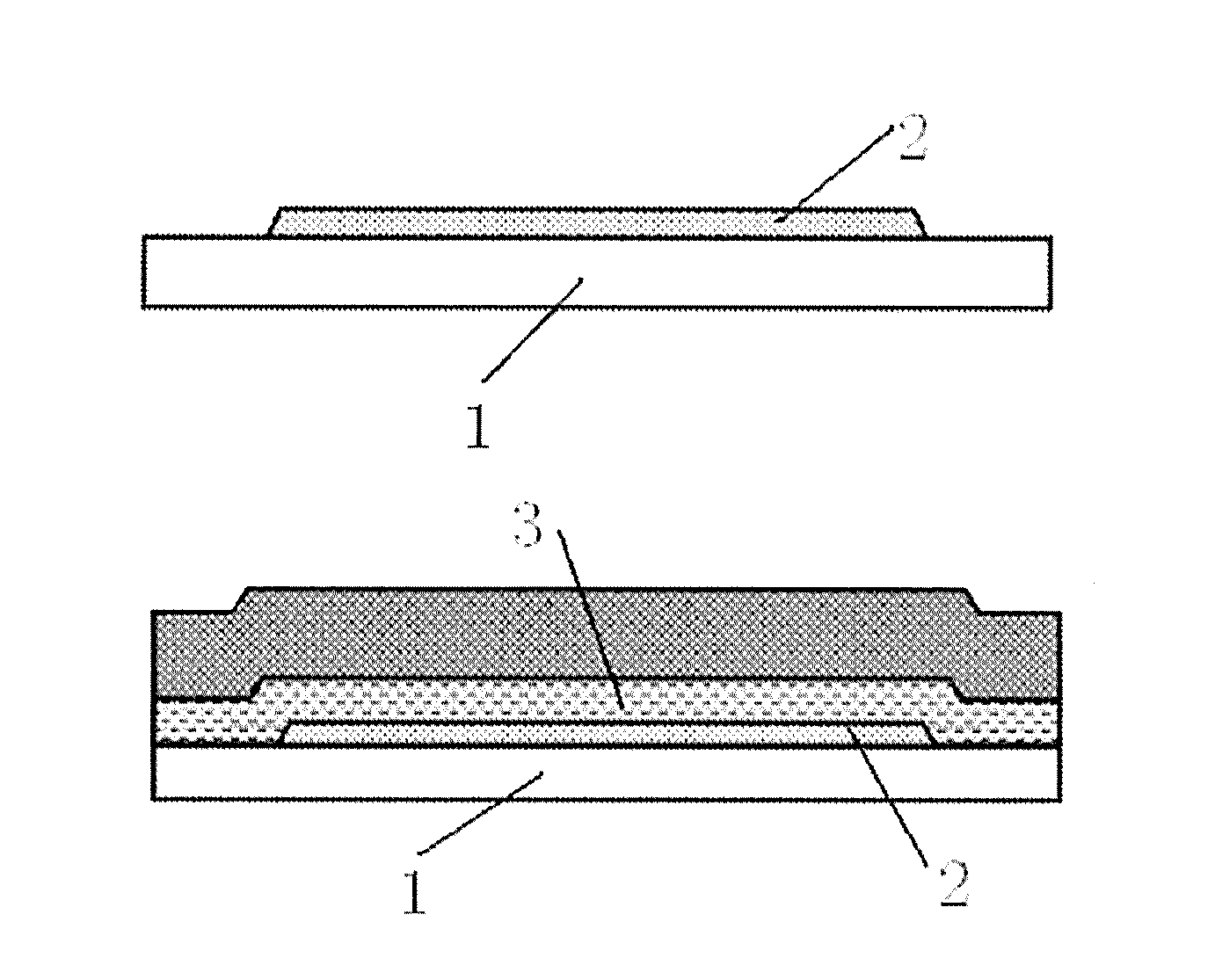
FIG. 1 is a cross-section structure diagram of a thin-film transistor with a fin-shape channel structure.
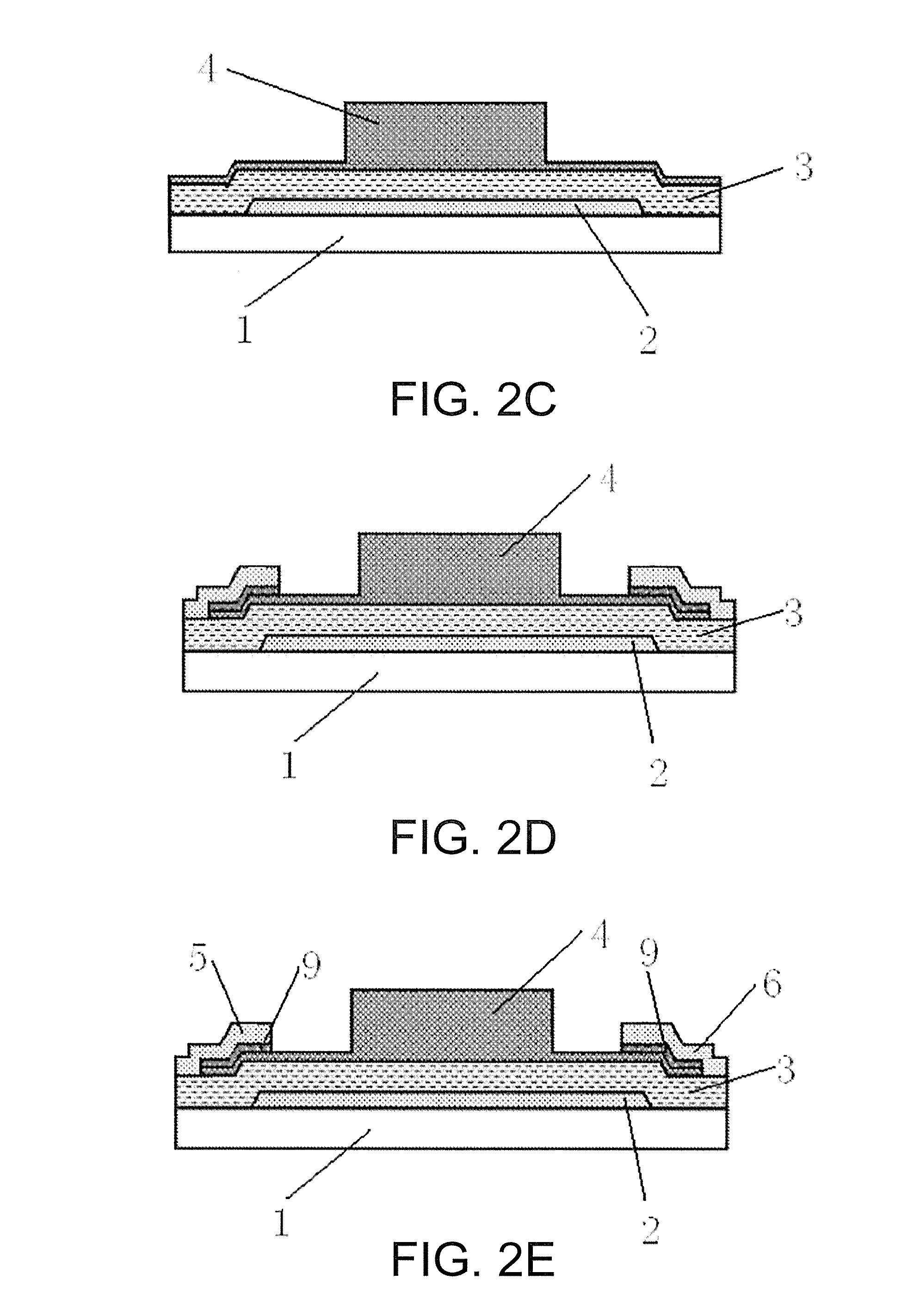
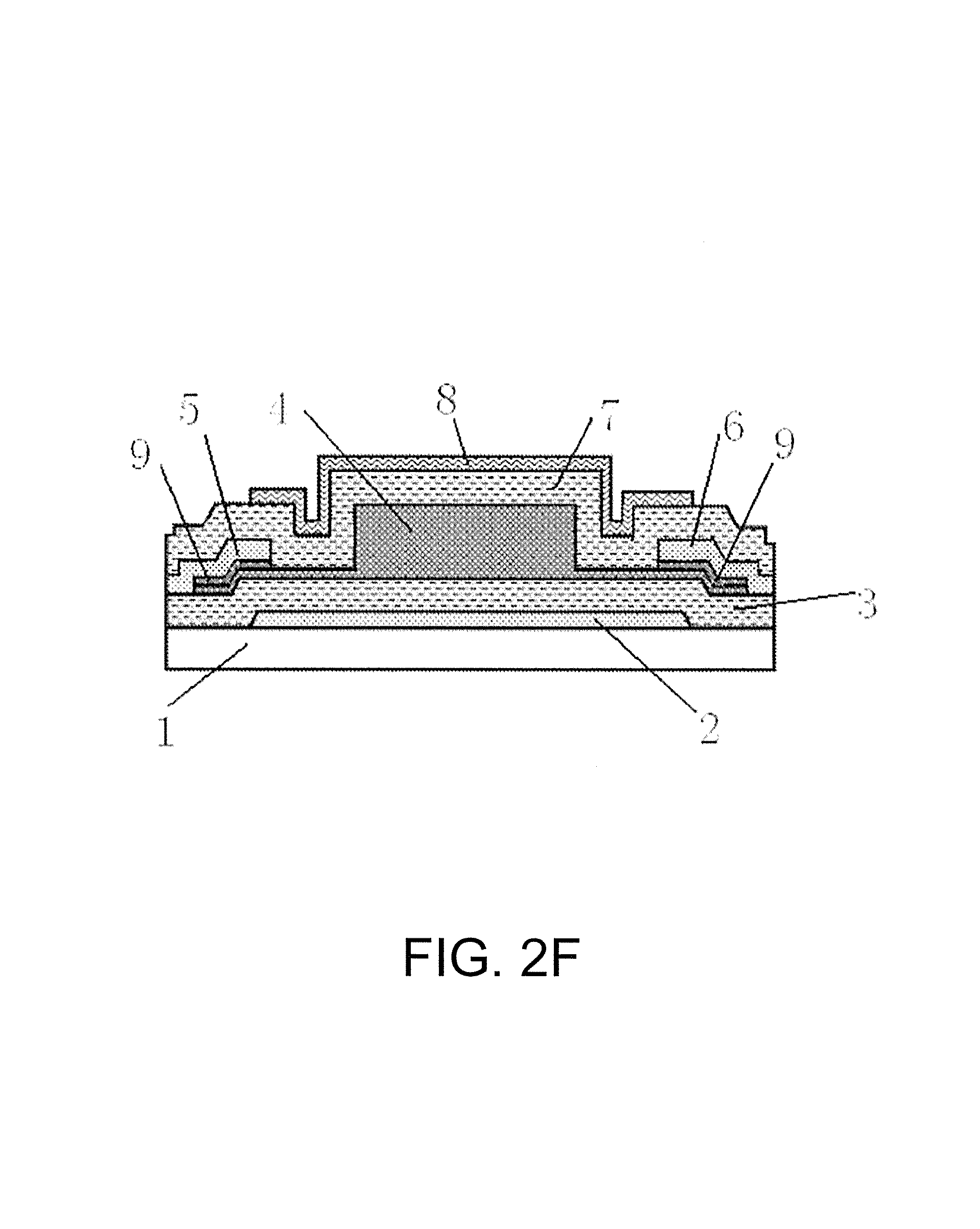
FIG. 2A to FIG. 2F are a preparation flow chart of a thin-film transistor with a fin-shape channel structure.
FIG. 3A and FIG. 3B are respectively an output characteristic curve and a transfer characteristic curve of the prepared device.
DETAILED DESCRIPTION OF THE PREFERED EMBODIMENT
The present invention is further described below in combination with accompanying drawings, but implementations of the present invention are not limited hereto.
As shown in FIG. 2A to FIG. 2F, it is a preparation method of a thin-film transistor structure with a three-dimensional fin-shape channel, the channel having a fin-shape structure which is thick in a middle and thin on both sides, process procedure and the method includes following steps:
(a) depositing and etching a bottom gate electrode 2 on a substrate 1;
(b) depositing a bottom dielectric layer 3 at an upper part of a structure obtained from the step (a), and sequentially depositing a semiconductor film on the bottom dielectric layer 3;
(c) etching the semiconductor film to obtain a fin-shape channel 4;
(d) successively depositing an Ohmic contact layer 9 and a source electrode 5 on the semiconductor film located at one side of the fin-type channel 4 and etching, and successively depositing the Ohmic contact layer 9 and a drain electrode 6 on the semiconductor film located at the other side and etching;
(e) depositing a top dielectric layer 7 and a top gate electrode 8 at an upper part of a structure obtained from the step (d); and
(f) etching the top gate electrode 8, and completing a preparation of a dual-gate fin-shape channel thin-film transistor.
As shown in FIG. 1, a thin-film transistor structure with a three-dimensional fin-shape channel structure prepared by the above-described method comprises: a substrate 1, a bottom gate electrode 2 located at an upper part of the substrate 1, a bottom dielectric layer 3 located at an upper part of the bottom gate electrode 2, a fin-shape channel 4 located at an upper part of the bottom dielectric layer 3, a source electrode 5 and a drain electrode 6 which are located at both sides of the fin-type channel 4, an Ohmic contact layer 9 among the source electrode 5, the drain electrode 6 and the fin-shape channel 4, a top dielectric layer 7 located at upper parts of the fin-shape channel 4, the source electrode 5 and the drain electrode 6, and a top gate electrode 8 located at an upper part of the top dielectric layer.
The present invention proposes a preparation method of a thin-film transistor with a fin-shape channel structure, which is composed of a series of photolithography and etches. The biggest difference between the thin-film transistor with the fin-shape channel structure prepared by this method and the thin-film transistor with a conventional planar channel structure is that a thickness of the semiconductor film in a channel region is increased while a thickness of a semiconductor film in a source-drain region is reduced.
Compared with the prior arts, the above-described thin-film transistor with the fin-shape channel structure has following characteristics: 1) for the thin-film transistor with a top gate electrode structure, an actual channel length is increased, alleviating a short channel effect, especially for a polysilicon thin-film transistor with a smaller device size, and a requirement of high-density integration is met since an overall device size does not increase; and 2) in a dual-gate photoelectric thin-film transistor, a sufficiently thick channel layer ensures a light absorption, while a sufficiently thin semiconductor film in contact with the source drain electrode ensures a low contact resistance, so that its output characteristic curve does not deteriorate.
The above-described preparation method of the thin-film transistor with the fin-shape channel structure may also be suitable for preparing a plurality of thin-film transistors with fin-shape structure and realize a parallel connection and a series connection among the thin-film transistors. Main application fields of the above-described thin-film transistor with the fin-shape channel structure include high resolution display, photoelectric detection and imaging, as well as biomedical sensors, etc.
FIG. 3A is a dark-state transfer characteristic curve of the thin-film transistor with the three-dimensional fin-shape channel, a control of a top gate to the channel is reflected in that the transfer characteristic curve shifts with a size of the top gate, that is, a sensitivity of a threshold voltage to a top gate voltage, wherein r is a sensitivity coefficient; and FIG. 3B is a transfer characteristic curve under light, and it can be seen that the transfer characteristic curve shifts with a light intensity, which illustrates that the device is sensitive to light, wherein r2 is sensitivity coefficient of the threshold voltage to a photovoltage.
The above-described implementations of the present invention do not constitute a limitation of the scope of protection of the present invention. Any amendments, equivalent replacements and improvements made within the spirit and principle of the present invention shall all be included within the scope of protection of the claims of the present invention.
* * * * *
D00000
D00001
D00002
D00003
D00004
XML
uspto.report is an independent third-party trademark research tool that is not affiliated, endorsed, or sponsored by the United States Patent and Trademark Office (USPTO) or any other governmental organization. The information provided by uspto.report is based on publicly available data at the time of writing and is intended for informational purposes only.
While we strive to provide accurate and up-to-date information, we do not guarantee the accuracy, completeness, reliability, or suitability of the information displayed on this site. The use of this site is at your own risk. Any reliance you place on such information is therefore strictly at your own risk.
All official trademark data, including owner information, should be verified by visiting the official USPTO website at www.uspto.gov. This site is not intended to replace professional legal advice and should not be used as a substitute for consulting with a legal professional who is knowledgeable about trademark law.