Electrophotographic photoconductor, manufacturing method thereof, and electrophotographic apparatus using the same
Kitagawa , et al. O
U.S. patent number 10,429,752 [Application Number 16/117,144] was granted by the patent office on 2019-10-01 for electrophotographic photoconductor, manufacturing method thereof, and electrophotographic apparatus using the same. This patent grant is currently assigned to FUJI ELECTRIC CO., LTD.. The grantee listed for this patent is FUJI ELECTRIC CO., LTD.. Invention is credited to Seizo Kitagawa, Kazuya Saito, Toshiki Takeuchi.


View All Diagrams
| United States Patent | 10,429,752 |
| Kitagawa , et al. | October 1, 2019 |
Electrophotographic photoconductor, manufacturing method thereof, and electrophotographic apparatus using the same
Abstract
Provided is a positively charged electrophotographic photoconductor, a manufacturing method thereof, and an electrophotographic apparatus using the same. The positively charged electrophotographic photoconductor includes an electroconductive support and a single layer-type photosensitive layer provided thereon including a charge generation material, a hole transport material, an electron transport material, and a mixed binder resin. Alternately, the positively charged electrophotographic photoconductor includes an electroconductive support; a charge transport layer provided on the electroconductive support and containing at least a hole transport material, and a binder resin; and a charge generation layer provided on the charge transport layer and including at least a charge generation material, a hole transport material, an electron transport material, and a mixed binder resin. In either embodiment, the mixed binder resin contains at least two resins including a polycarbonate-based resin selected to provide the mixed binder resin with a water vapor permeability ranging from 5 to 13 g/m.sup.2day.
| Inventors: | Kitagawa; Seizo (Matsumoto, JP), Takeuchi; Toshiki (Guang Dong, CN), Saito; Kazuya (Matsumoto, JP) | ||||||||||
|---|---|---|---|---|---|---|---|---|---|---|---|
| Applicant: |
|
||||||||||
| Assignee: | FUJI ELECTRIC CO., LTD.
(Kawasaki-Shi, Kanagawa, JP) |
||||||||||
| Family ID: | 63253572 | ||||||||||
| Appl. No.: | 16/117,144 | ||||||||||
| Filed: | August 30, 2018 |
Prior Publication Data
| Document Identifier | Publication Date | |
|---|---|---|
| US 20180373172 A1 | Dec 27, 2018 | |
Related U.S. Patent Documents
| Application Number | Filing Date | Patent Number | Issue Date | ||
|---|---|---|---|---|---|
| PCT/JP2017/007253 | Feb 24, 2017 | ||||
| Current U.S. Class: | 1/1 |
| Current CPC Class: | G03G 5/14756 (20130101); G03G 5/0564 (20130101); G03G 5/0672 (20130101); C08G 64/06 (20130101); G03G 5/0696 (20130101); G03G 5/0525 (20130101); G03G 5/0616 (20130101); G03G 5/0614 (20130101); G03G 5/047 (20130101); G03G 5/051 (20130101); G03G 5/0668 (20130101); G03G 5/0596 (20130101); G03G 5/0592 (20130101) |
| Current International Class: | G03G 5/00 (20060101); C08G 64/06 (20060101); G03G 5/05 (20060101); G03G 5/147 (20060101); G03G 5/047 (20060101); G03G 5/06 (20060101) |
| Field of Search: | ;430/96,66 |
References Cited [Referenced By]
U.S. Patent Documents
| 4882253 | November 1989 | Kato et al. |
| 2011/0091799 | April 2011 | Nakamura et al. |
| 2012/0003574 | January 2012 | Kitagawa et al. |
| 2014/0199619 | July 2014 | Kitagawa et al. |
| 2015/0346619 | December 2015 | Kitagawa et al. |
| H03-256050 | Nov 1991 | JP | |||
| H04-241359 | Aug 1992 | JP | |||
| H04-242259 | Aug 1992 | JP | |||
| H05-12702 | Feb 1993 | JP | |||
| H05-45915 | Feb 1993 | JP | |||
| H05-30262 | May 1993 | JP | |||
| H05-47822 | Jul 1993 | JP | |||
| H07-160017 | Jun 1995 | JP | |||
| 2001-142234 | May 2001 | JP | |||
| 2003-228184 | Aug 2003 | JP | |||
| 2004-240056 | Aug 2004 | JP | |||
| 2007-121733 | May 2007 | JP | |||
| 2007-163523 | Jun 2007 | JP | |||
| 2007-206130 | Aug 2007 | JP | |||
| 2007-256768 | Oct 2007 | JP | |||
| 2009-288569 | Dec 2009 | JP | |||
| 2010-276699 | Dec 2010 | JP | |||
| 2014-092594 | May 2014 | JP | |||
| 2014-109683 | Jun 2014 | JP | |||
| 2015-12233 | Apr 2015 | TW | |||
| WO-2009/104571 | Aug 2009 | WO | |||
| WO-2013/021430 | Feb 2013 | WO | |||
Attorney, Agent or Firm: Rabin & Berdo, P.C.
Parent Case Text
CROSS-REFERENCE TO RELATED APPLICATIONS
This non-provisional application is a continuation of International Application No. PCT/JP2017/007253 filed on Feb. 24, 2017, the entire contents of which are incorporated herein by reference.
Claims
What is claimed is:
1. A positively charged electrophotographic photoconductor, comprising an electroconductive support; and a single layer-type photosensitive layer provided on the electroconductive support and including a charge generation material, a hole transport material, an electron transport material, and a mixed binder resin that comprises at least two resins including a polycarbonate-based resin, wherein the at least two resins are selected to provide the mixed binder resin with a water vapor permeability ranging from 5 to 13 g/m.sup.2day.
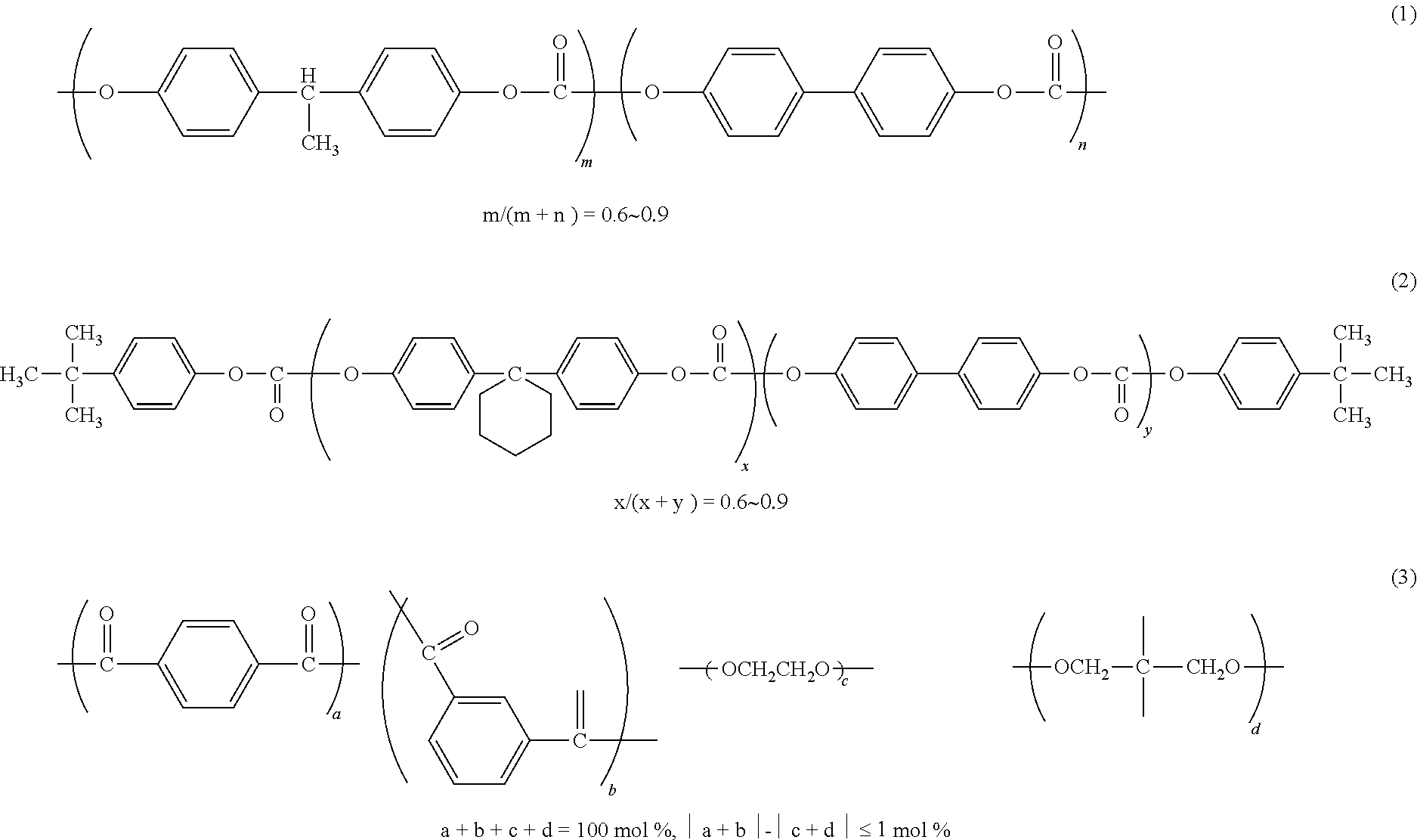
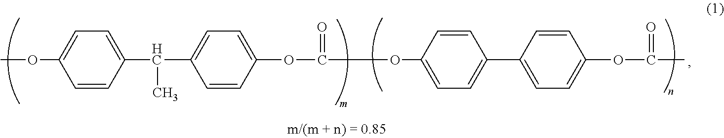
2. The electrophotographic photoconductor according to claim 1, wherein the mixed binder resin contains a resin having a repeating unit represented by formula (1) below: ##STR00013##
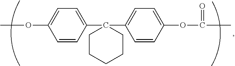
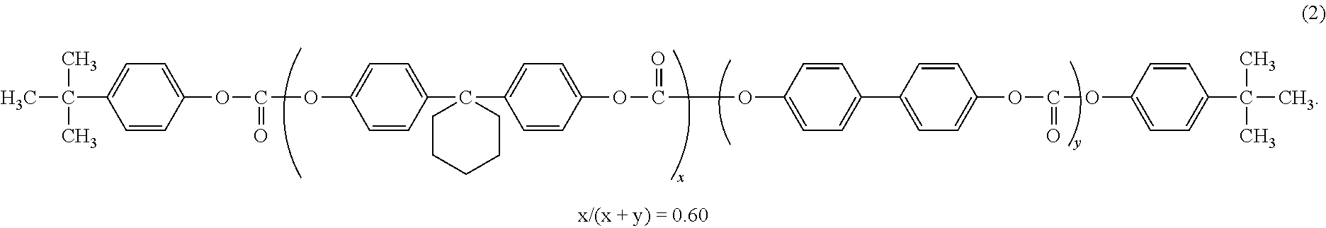
3. The electrophotographic photoconductor according to claim 1, wherein the mixed binder resin contains a resin having a repeating unit represented by formula (1) below and a repeating unit represented by formula (2) below: ##STR00014##
4. The electrophotographic photoconductor according to claim 1, wherein the mixed binder resin contains a resin having a repeating unit represented by formula (2) below and a repeating unit represented by formula (3) below: ##STR00015##
5. The electrophotographic photoconductor according to claim 1, wherein the charge generation material comprises at least titanyl phthalocyanine.
6. A method of producing the electrophotographic photoconductor according to claim 1, wherein the single layer-type photosensitive layer containing a mixed binder resin is formed by a dip coating method.
7. An electrophotographic apparatus equipped with the electrophotographic photoconductor according to claim 1.
8. The electrophotographic apparatus according to claim 7, wherein the electrophotographic apparatus is equipped with a contact developing system that is a nonmagnetic one-component contact developing system using polymerized toner in a cleaner-less process.
9. The positively charged electrophotographic photoconductor according to claim 1, wherein the mixed binder resin contains a resin having a repeating unit represented by formula (1) or formula (2) below and a repeating unit represented by formula (3) below: ##STR00016##
10. A positively charged electrophotographic photoconductor, comprising: an electroconductive support; a charge transport layer provided on the electroconductive support and containing at least a hole transport material and a binder resin; and a charge generation layer provided on the charge transport layer and including at least a charge generation material, a hole transport material, an electron transport material, and a mixed binder resin that comprises at least two resins including a polycarbonate-based resin, wherein the at least two resins are selected to provide the mixed binder resin of the charge generation layer with a water vapor permeability ranging from 5 to 13 g/m.sup.2day.
11. The electrophotographic photoconductor according to claim 10, wherein the mixed binder resin contains a resin having a repeating unit represented by formula (1) below: ##STR00017##
12. The electrophotographic photoconductor according to claim 10, wherein the mixed binder resin contains a resin having a repeating unit represented by formula (1) below and a repeating unit represented by formula (2) below: ##STR00018##
13. The electrophotographic photoconductor according to claim 10, wherein the mixed binder resin contains a resin having a repeating unit represented by formula (2) below and a repeating unit represented by formula (3) below: ##STR00019##
14. The electrophotographic photoconductor according to claim 10, wherein the charge generation material comprises at least titanyl phthalocyanine.
15. A method of producing the electrophotographic photoconductor according to claim 10, wherein the charge generation layer containing a mixed binder resin is formed by a dip coating method.
16. An electrophotographic apparatus equipped with the electrophotographic photoconductor according to claim 10.
17. The electrophotographic apparatus according to claim 16, wherein the electrophotographic apparatus is equipped with a contact developing system that is a nonmagnetic one-component contact developing system using polymerized toner in a cleaner-less process.
18. The positively charged electrophotographic photoconductor, according to claim 10, wherein the mixed binder resin in the charge generation layer contains a resin having a repeating unit represented by formula (1) or formula (2) below and a repeating unit represented by formula (3) below: ##STR00020##
19. The positively charged electrophotographic photoconductor, according to claim 10, wherein the water vapor permeability of the binder resin of the charge transport layer is 4 g/m.sup.2day or less.
Description
BACKGROUND OF THE INVENTION
1. Field of the Invention
The present invention relates to an electrophotographic photoconductor (hereinafter simply referred to as "photoconductor") and an electrophotographic apparatus using the same, and more particularly to an electrophotographic photoconductor for use in an electrophotographic printer, copying machine, fax machine and the like, and to an electrophotographic apparatus using the same.
2. Background of the Related Art
Generally, an image forming apparatus using an electrophotographic system such as a printer, a copying machine, and a facsimile machine comprises a photoconductor as an image carrier; a charging apparatus for uniformly charging the surface of the photoconductor; an exposure apparatus for writing an electrical image (electrostatic latent image) corresponding to the image on the surface of the photoconductor; a development apparatus for developing the electrostatic latent image with a toner to form a toner image; and a transfer apparatus for transferring the toner image onto a transfer sheet. The image forming apparatus further comprises a fixing apparatus for making the toner on this transfer paper to be fused on the transfer paper.
For such an image forming apparatus, a photoconductor to be used may vary depending on the concept of the apparatus. At present, an organic photoconductor (OPC) in which an organic pigment is dispersed in a resin has been widely used because of its excellent stability, cost, and ease of handling, except for an inorganic photoconductor such as Se and a-Si used for a large machine and/or a high-speed machine. An organic photoconductor is generally of negatively charged type, whereas an inorganic photoconductor is of positively charged type. It is because hole transport materials having a good hole transport function have been developed for negatively charged type organic photoconductors, whereas electron transport materials having a good electron transport function have been hardly developed for positively charged type organic photoconductors.
On the other hand, in the negative charging process for such a negatively charged type organic photoconductor, since the negative corona discharge generates overwhelmingly larger amount of ozone compared to the positive corona discharge, the amount of ozone generation is suppressed by adopting a contact charging system such as roller charging or brush charging. However, this contact charging system is disadvantageous in terms of cost and high-quality image because of its tendency of generating contamination of the charging member and difficulty in homogenization of surface potential of the photoconductor, as compared with the non-contact positive charging system.
In order to solve these problems, it is effective to apply a positively charged type organic photoconductor. There is a need for a high performance positively charged type organic photoconductor. In addition to the merit peculiar to the positive charging system as described above, the positively charged type organic photoconductor is advantageous in less lateral diffusion of a carrier and excellent dot reproducibility (resolution and gradation) because the position of the carrier generated is generally near the surface of the photosensitive layer. For this reason, positively charged type organic photoconductors have been put on the market in various fields where resolution improvement has been advanced.
As a low-cost, compact, high-resolution and high-speed monochrome or color machine making full use of this advantage, there is a cleaner-less process apparatus of nonmagnetic one-component contact developing system using positively charged polymerized toner which is expanding the market because high image quality is obtained.
Positively charged type organic photoconductors are roughly divided into four types of layer constitutions as described below, and various kinds have been conventionally proposed. The first one is a function separation type photoconductor having two-layer constitution in which a charge transport layer and a charge generation layer are sequentially laminated on an electroconductive support (see, for example, Patent Document 1). The second one is a function separation type photoconductor having a three-layer constitution in which a surface protective layer is laminated on the two-layer structure mentioned above (see, for example, Patent Document 2). The third one is a function separation type photoconductor having a two-layer constitution, in which a charge generation layer and a charge (electron) transport layer are laminated in the order contrary to the first one (for example, see Patent Document 3). The fourth one is a single layer type photoconductor in which a charge generation material, a hole transport material and an electron transport material are dispersed in the same layer (see, for example, Patent Document 3). In the classifications of the above four types, the presence or absence of an undercoat layer is not considered.
Among them, the fourth one, i.e., a single layer type photoconductor has been studied in detail and has been widely applied. However, in a single layer type photoconductor, there is a limit to achieving both high sensitivity/high speed and high durability. Therefore, a laminated type positively charged photoconductor in which a charge transport layer and a charge generation layer are laminated sequentially has also been proposed (see, for example, Patent Document 4). The layer structure of this laminated type positively charged photoconductor is similar to the layer structure of the first one described above. However, the charge generation material contained in the charge generation layer can be reduced and, at the same time, the electron transport material can be included to provide a thicker film similar to the charge transport layer of the lower layer, and the amount of the hole transport material added in the charge generation layer can be reduced. Accordingly, the resin percentage in the charge generation layer can be set to be higher than that in the conventional single layer type, making it easy to achieve both high sensitivity and high durability.
RELATED ART DOCUMENTS, PATENT DOCUMENTS
PATENT DOCUMENT 1: JPH05-30262B; PATENT DOCUMENT 2: JPH05-47822B; PATENT DOCUMENT 3: JPH05-45915A; and PATENT DOCUMENT 4: JP2009-288569A
However, both single layer type positively charged organic photoconductor and laminate type positively charged organic photoconductor can provide high image quality when used in the cleaner-less process of the nonmagnetic one-component contact developing system using the above-mentioned polymerized toner, but they are suffered from problems, that is, a mixture of toner and paper powder adheres to be deposited onto the surface of the photoconductor and thus cannot be removed from the surface, during printing in a high-temperature and high-humidity environment.
That is, in this case, a material deposited onto the surface of the photoconductor absorbs moisture in the air, resulting in reduced resistance value just below it, locally dropped potential and leakage, as well as tendency to generate minute image defects, i.e., black spots for a monochrome machine and color spots for a color machine, during the initial printing in a high-temperature and high-humidity environment.
The mixture of toner and paper powder has high hygroscopicity. Therefore, the deposited matter on the surface of the photosensitive layer continuously absorbs moisture from the atmosphere, and supplies the moisture into the photosensitive layer. Therefore, the resistance value of the photosensitive layer immediately below the deposited matter is extremely lower than those of other portions, and, at the time of printing, the blank portion (charged portion) is accompanied with charge potential loss due to local reduction and/or leakage of charge potential while the toner is developed, producing black spots or color spots. Here, the diameter of a black spot and a color spot is about 0.5 mm or less.
For this reason, countermeasures have been conventionally taken to increase the pressure resistance by the following methods. The first countermeasure is to make the film thickness of the photosensitive layer thicker than the conventional one, for example, the film thickness of 20 to 30 .mu.m is increased to 31 to 40 .mu.m. Alternatively, it has also been conducted to reduce the roughness of the substrate by changing the processing condition of the substrate (electroconductive support) from the cutting processing to the mirror surface processing; or to add a resin film or an anodic oxidation coating as a barrier layer between the substrate and the photosensitive layer.
However, since they do not fundamentally inhibit the deposition of the mixture of toner and paper powder onto the surface of the photosensitive layer, they fail to eliminate the generation of minute black spots. Actually, as shown in FIG. 4, this is evident from the fact that the correlation between the pressure resistance (leakage start time) of the photosensitive layer and the number of minute black spots generated is not always clear.
Accordingly, an object of the present invention is to solve the above problems and to provide an electrophotographic photoconductor which provides a stable high-quality image in any environment without generating minute black spots or color spots during the initial printing in a high-temperature and high-humidity environment even when mounted on a high-quality/high-speed monochrome machine or a tandem color machine equipped with a cleaner-less process of nonmagnetic one-component contact developing system using polymerized toner; a manufacturing method thereof; and an electrophotographic apparatus using the same.
SUMMARY OF THE INVENTION
The present inventors have conducted intensive studies on measures to prevent generation of minute black spots and color spots due to deposition of a mixture of toner and paper powder on the surface of the photoconductor in a high-temperature and high-humidity environment. As a result, the present inventors have found that using a resin having a water vapor permeability in a predetermined range as a resin used for the outermost layer of the photoconductor can suppress the generation of minute black spots and the like during the initial printing in a high-temperature and high-humidity environment.
That is, the electrophotographic photoconductor according to the first aspect of the present invention, which is a positively charged electrophotographic photoconductor, comprising: an electroconductive support; and a single layer type photosensitive layer provided on the electroconductive support, which includes a charge generation material, a hole transport material, an electron transport material and a binder resin; wherein the binder resin contains a polycarbonate-based resin and the water vapor permeability of the binder resin is in the range from 5 to 13 g/m.sup.2day.
That is, the electrophotographic photoconductor according to the second aspect of the present invention, which is a positively charged electrophotographic photoconductor, comprising: an electroconductive support; a charge transport layer containing at least a hole transport material and a binder resin, and provided on the electroconductive support; and a charge generation layer provided on the charge transport layer, which includes at least a charge generation material, a hole transport material, an electron transport material and a binder resin; wherein the binder resin in the charge generation layer contains a polycarbonate-based resin and the water vapor permeability of the binder resin is in the range from 5 to 13 g/m.sup.2day.
The aforementioned binder resin having the water vapor permeability of 5 to 13 g/m.sup.2day may contain a resin having a repeating unit represented by formula (1) below. Alternatively, it may contain a resin having a repeating unit represented by the formula (1) below and a resin having a repeating unit represented by formula (2) below. Furthermore, the binder resin having the aforementioned water vapor permeability in the range from 5 to 13 g/m.sup.2day may contain a resin having a repeating unit represented by the formula (2) below and a resin having a repeating unit represented by formula (3) below. In the photoconductor of the present invention, it is preferable that the charge generation material contains at least titanyl phthalocyanine.
##STR00001##
A method for producing an electrophotographic photoconductor according to the third aspect of the present invention is a method for manufacturing the electrophotographic photoconductor mentioned above, characterized in that a layer which contains a binder resin having the water vapor permeability in the range from 5 to 13 g/m.sup.2day is formed using a dip coating method.
An electrophotographic apparatus according to the fourth aspect of the present invention is equipped with the electrophotographic photoconductor mentioned above.
The electrophotographic apparatus may be provided with a cleaner-less process of a nonmagnetic one-component contact developing system using polymerized toner.
Effects of the Invention
According to the present invention, it is possible to attain a electrophotographic photoconductor which provides a stable, high-quality image in any environment without generating minute black spots or color spots during the initial printing in high-temperature and high-humidity environment even when mounted on a high-quality/high-speed monochrome machine or a tandem color machine equipped with a cleaner-less process of nonmagnetic one-component contact developing system using polymerized toner; a manufacturing method thereof; and an electrophotographic apparatus using the same.
BRIEF DESCRIPTION OF THE DRAWINGS
FIG. 1 is a schematic cross-sectional view showing a configuration example of a single layer type positively charged electrophotographic photoconductor of the present invention;
FIG. 2 is a schematic cross-sectional view showing a configuration example of the laminate type positively charged electrophotographic photoconductor of the present invention;
FIG. 3 is a schematic configuration diagram showing an example of an electrophotographic apparatus of the present invention;
FIG. 4 is a graph showing the relationship between the leakage start time and the number of the generated minute black spots; and
FIG. 5 is an explanatory view showing an evaluation image used for evaluating ghost/fog in Examples.
DETAILED DESCRIPTION OF THE INVENTION
The embodiments of the present invention will be hereinafter described in detail with reference to the drawings. The present invention is not limited at all by the following explanation.
FIG. 1 and FIG. 2 show schematic cross-sectional views showing a configuration example of the electrophotographic photoconductor of the present invention. FIG. 1 shows a single layer type positively charged electrophotographic photoconductor comprising a single layer type photosensitive layer 3 on an electroconductive support 1 with an undercoat layer 2 interposed therebetween; FIG. 2 shows a laminate type positively charged electrophotographic photoconductor comprising a charge transport layer 4 and a charge generation layer 5 sequentially formed on an electroconductive support 1 with an undercoat layer 2 interposed therebetween.
In the electrophotographic photoconductor of the present invention of both single layer type and laminate type, the water vapor permeability of the binder resin contained in the outermost layer is in the range from 5 to 13 g/m.sup.2day, particularly preferably in the range from 6 to 12 g/m.sup.2day. Using the resin contained in the outermost layer which has the water vapor permeability in a predetermined range, moisture adsorbed on the surface of the photoconductor may become uniform, and even in a high-temperature and high-humidity environment, deposition of a mixture of toner and paper powder as well as generation of minute black spots and color spots during the initial printing can be suppressed. When the water vapor permeability of the binder resin contained in the outermost layer is less than 5 g/m.sup.2day, the adsorbed moisture tends to be unevenly distributed, and the mixture of toner and paper powder tends to deposit more easily, and when it exceeds 13 g/m.sup.2day, the film density decreases, resulting in increased water content and reduced resistance value, or the number of the generated black spots or color spots may be increased due to the influence of the discharge produced gas, and image fogging may be generated due to reduced charge potential. In the present invention, the water vapor permeability of the binder resin contained in the outermost layer means, in the case where two or more binder resins are contained, the water vapor permeability of a mixture of the two or more binder resins.
Specifically, as the binder resin used in the present invention, it is preferable to use, as an essential resin, a polycarbonate-based resin such as a bisphenol A type, a bisphenol Z type, a bisphenol A type-biphenyl copolymer or the like depending on the dispersion stability and mechanical strength of the charge generation material used in a combination thereof, which is preferably mixed with an appropriate amount of an arbitrary resin having the water vapor permeability higher than that of the polycarbonate-based resin such as a polystyrene-based resin, a polyester-based resin, a polyarylate-based resin or the like to obtain a desired water vapor permeability.
As the polycarbonate-based resin, for example, a resin having a repeating unit represented by formula (1) below can be suitably used. In addition, a resin having a repeating unit represented by the formula (1) below and a resin represented by formula (2) below are also preferably used in combination. In addition, a polycarbonate-based resin having a repeating unit represented by the formula (2) below and a polyester resin having a repeating unit represented by formula (3) below are also preferably used in combination. In the case of a resin having repeating units represented by the formulae below, the value of the water vapor permeability changes only by about .+-.5%, so long as the ratio of the repeating units satisfy the following:
##STR00002##
Single Layer Type Photoconductor
Electroconductive Support
The electroconductive support 1 plays a role as an electrode of a photoconductor and at the same time it serves as a support for respective layer constituting the photoconductor. The electroconductive support 1 may be in any shape such as a cylindrical shape, a plate shape, a film shape and the like, and in terms of material, in addition to metals such as aluminum, stainless steel, and nickel, a glass and a resin having electroconductively-treated surface may also be used.
Undercoat Layer
The undercoat layer 2 is basically unnecessary in the present invention, but it can be provided in order to further improve the reliability, as needed. The undercoat layer 2 is composed of a layer containing a resin as a main component, a metal oxide film such as an alumite etc., and is used for the purpose of improving the adhesion between the electroconductive support and the charge transport layer, as well as for the purpose of controlling charge injected into the photosensitive layer. Examples of the resin material used for the undercoat layer include insulating polymers such as casein, polyvinyl alcohol, polyamide, melamine, cellulose; and electroconductive polymers such as polythiophene, polypyrrole, polyaniline. These resins can be used alone or mixed and used in an appropriate combination. Metal oxides such as titanium dioxide and zinc oxide can also be contained in these resins.
Photosensitive Layer
The single layer type photosensitive layer 3 is mainly composed of a charge generation material, a hole transport material, an electron transport material and a binder resin. Here, the single layer type photosensitive layer 3 may be formed on the outer periphery of the electrophotographic photoconductor farthest from the electroconductive support 1. The electrophotographic photoconductor may be mounted on the electrophotographic apparatus in a state where the surface of the photosensitive layer 3 farthest from the electroconductive support 1 may come into contact with the atmosphere.
Charge Generation Material
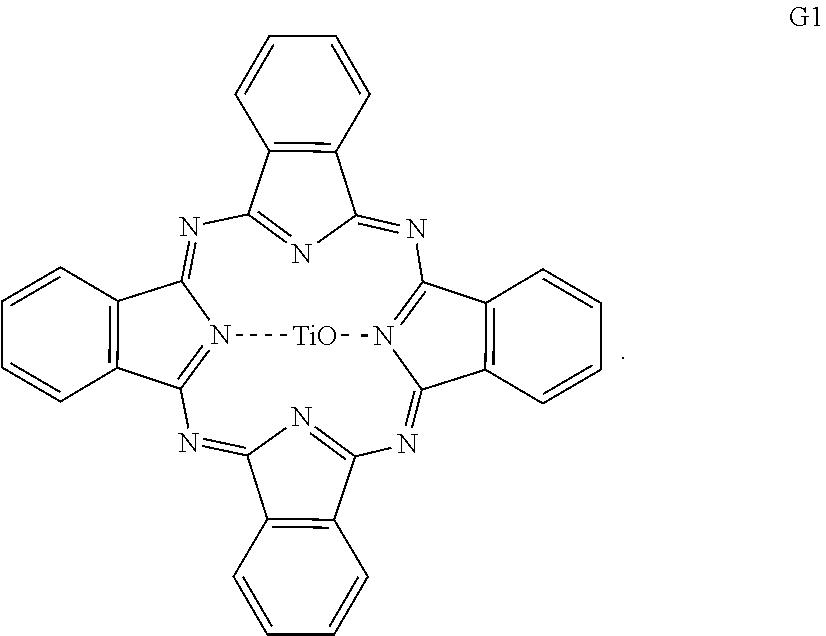
As the charge generation material, X-type metal-free phthalocyanine may be used alone, or .alpha.-type titanyl phthalocyanine, .beta.-type titanyl phthalocyanine, Y-type titanyl phthalocyanine, .gamma.-type titanyl phthalocyanine, amorphous-type titanyl phthalocyanine, gallium phthalocyanine may be used alone or in an appropriate combination thereof. It is possible to select a suitable material according to the light wavelength region of the exposure light source used for image formation. Titanyl phthalocyanine with high quantum efficiency is optimal from the viewpoint of improved sensitivity.
Hole Transport Material
As a hole transport material, various hydrazone compounds, styryl compounds, stilbene compounds, enamine compounds, diamine compounds, butadiene compounds, indole compounds, triphenylamine compounds, triphenyldiamine compounds and the like can be used alone or in an appropriate combination. Among them, a styryl compound containing a triphenylamine skeleton is preferable from the viewpoint of cost and performance.
Electron Transport Material
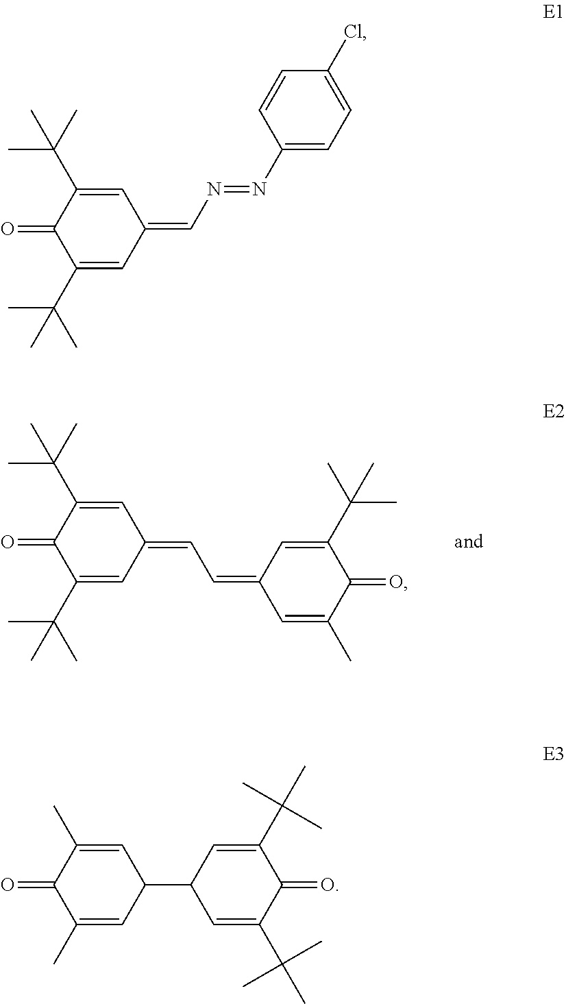
As electron transport materials, those having higher mobility is more preferred. A quinone type material such as benzoquinone, stilbenequinone, naphthoquinone, dinaphthoquinone, diphenoquinone, phenanthrenequinone, azoquinone, or a tetranaphthalenecarboxylic acid diimide type material are preferred. From the viewpoint of injectability into the charge transport layer and compatibility with the binder resin, it is also preferable to use a material alone or two or more materials to increase the content of the electron transport material while suppressing the precipitation.
Binder Resin
As described above, as the binder resin, various kinds of polycarbonate-based resins as an essential component, and arbitrary resins selected from polystyrene-based resins, polyester-based resins, polyarylate-based resins and the like are appropriately used in a combination in order to control the water vapor permeability.
Other Additives
In the photosensitive layer 3, a deterioration inhibitor such as an antioxidant or a light stabilizer may be incorporated for the purpose of improving environmental resistance and stability against harmful light, if desired. Examples of the compounds used for such purposes include chromanol derivatives such as tocopherol and esterified compounds, polyarylalkane compounds, hydroquinone derivatives, etherified compounds, dietherified compounds, benzophenone derivatives, benzotriazole derivatives, thioether compounds, phenylenediamine derivatives, phosphonic acid esters, phosphorous acid esters, phenol compounds, hindered phenol compounds, amine compounds and the like.
A leveling agent such as a silicone oil or a fluorine-based oil may be contained for the purpose of improving the leveling property of the formed film and imparting lubricity. Further, for the purpose of adjusting the film hardness, reducing the friction coefficient, imparting lubricity, etc., a metal oxide such as silicon oxide (silica), titanium oxide, zinc oxide, calcium oxide, aluminum oxide (alumina), zirconium oxide; metal sulfates such as barium sulfate and calcium sulfate; and metal nitrides such as silicon nitride and aluminum nitride, in the form of fine particles, may be contained. Further, other known additives may be contained, if necessary, so long as electrophotographic characteristics may not be significantly impaired.
Composition
The mass ratio of the total functional materials (charge generation material, electron transport material and hole transport material) to the binder resin in the photosensitive layer 3 is preferably set in the range from 45:55 to 55:45 in order to obtain desired characteristics. When the mass ratio of the functional material is more than 55% by mass in the photosensitive layer, in other words, when the amount of the binder resin is less than 45% by mass, the amount of film reduction will be increased and the durability will be decreased, and the glass transition point will be decreased, resulting in insufficient creep strength. Accordingly, toner filming as well as filming of external additives and paper powder are liable to occur, and the amount of the generated minute black spots and the like due to deposited mixture of toner and paper powder in a high-temperature and high-humidity environment like the present example may be increased. In addition, contact member contamination (creep deformation) tends to occur easily, and contamination due to oil and fat such as grease and sebum contamination may also be worsened. When the mass ratio of the functional material is less than 45% by mass in the photosensitive layer 3, that is, when the content of the binder resin exceeds 55% by mass, it is difficult to obtain desired sensitivity characteristics, which may be unsuitable for practical use. Generally, from the viewpoint of suppressing member contamination, oil and fat contamination and sebum contamination while ensuring durability, it is desirable to increase the percentage of the binder resin.
The content ratio of the charge generation material is preferably from 0.5 to 3% by mass, more preferably from 0.8 to 1.8% by mass, of the entire film. When the amount of the charge generation material is too small, the sensitivity characteristics become insufficient, and the occurrence of interference fringes increases. On the other hand, when the amount of the charge generation material is too much, the charging characteristics and fatigue characteristics (stability in repeated use) tend to be insufficient.
The mass ratio of the electron transport material to the hole transport material may vary within the range of 1:1 to 1:4, but it is generally more preferable to use the materials in the range of 2:3 to 1:3 from the viewpoint of sensitivity characteristics, charging characteristics and fatigue characteristics, based on transporting balance of holes and electrons.
Solvent
Examples of the solvent used for forming the photosensitive layer 3 include halogenated hydrocarbons such as dichloromethane, dichloroethane, chloroform, carbon tetrachloride, chlorobenzene and the like; ethers such as dimethyl ether, diethyl ether, tetrahydrofuran, dioxane, dioxolane, ethylene glycol dimethyl ether, diethylene glycol dimethyl ether; ketones such as acetone, methyl ethyl ketone, cyclohexanone, which may be appropriately selected from the viewpoints of solubility, liquid stability and coatability of the respective materials.
Film Thickness
The film thickness of the photosensitive layer 3 is preferably in the range from 15 to 40 .mu.m, more preferably 20 to 35 .mu.m, still more preferably 25 to 30 .mu.m from the viewpoint of ensuring practically effective performance.
Laminate Type Photoconductor
Electroconductive Support
The electroconductive support 1 is similar to the one for the single-layer type photoconductor.
Undercoat Layer
Also, an undercoat layer 2 is similar to the one for the single-layer type photoconductor and is basically unnecessary in the present invention, but, in order to improve the reliability, it may be appropriately provided as necessary.
Charge Transport Layer
The charge transport layer 4 is mainly composed of a hole transport material and a binder resin.
Hole Transport Material
The hole transport material used for the charge transport layer 4 is similar to the one for the single layer type photoconductor, but from the viewpoint of smooth charge transfer from the charge generation layer 5 to the charge transport layer 4, it is desirable to use the same material as that contained in the charge generation layer 5.
Binder Resin
As the binder resin of the charge transport layer 4, the same one as in the single layer type can be used. Since it is an inner layer, mechanical strength is not required so much, rather it is required to be hardly eluted when the charge generation layer 5 is applied. From such viewpoints, a resin which is hardly eluted in the solvent of the coating liquid for forming the charge generation layer 5 is preferable, and such a resin having a high molecular weight is preferably used. In relation to the binder resin of the charge generation layer 5, the water vapor permeability of the binder resin of the charge transport layer 4 is preferably lower than the water vapor transmission rate of the binder resin of the charge generation layer 5. Since deterioration easily occurs when the discharge produced gas enters the charge transport layer 4, suppressing the water vapor permeability of the charge transport layer 4 to a lower level is effective in preventing deterioration. Specifically, the water vapor permeability of the binder resin of the charge transport layer 4 is preferably 4 g/m.sup.2day or less, more preferably 3 g/m.sup.2day or less.
Other Additives
In the charge transport layer 4, a deterioration inhibitor such as an antioxidant or a light stabilizer may be incorporated for the purpose of improving environmental resistance and stability against harmful light, if desired. As compounds used for such a purpose, the same compounds as those mentioned for the single layer type photosensitive layer can be used.
Furthermore, in the charge transport layer 4, similar to the single layer type photosensitive layer, a leveling agent such as a silicone oil or a fluorine-based oil may be contained for the purpose of improving the leveling property of the formed film and imparting lubricity. Further, for the purpose of adjusting the film hardness, reducing the friction coefficient, imparting lubricity, and the like, fine particles of various metal oxides, metal sulfates, metal nitrides similar to those mentioned for the single layer type photosensitive layer may be contained. Further, other known additives may be contained so long as electrophotographic characteristics may not be significantly impaired, if necessary.
Composition
The mass ratio of the hole transport material and the binder resin in the charge transport layer 4 is in the range from 1:3 to 3:1 (25:75 to 75:25), suitably 7:13 to 13:7 (35:65 to 65:35). When the content of the hole transport material is less than 25% by mass in the charge transport layer 4, the transport function generally becomes insufficient, the residual potential becomes high, the environment dependency of the potential of the exposed portion in the device becomes large. Thus, the environmental stability of the image quality deteriorates so that it might become unsuitable for use. On the other hand, when the content of the hole transport material exceeds 75% by mass in the charge transport layer 4, that is, when the binder resin is less than 25% by mass in the charge transport layer 4, harmful effects of elution might occur when the charge generation layer 5 is applied.
Solvent
Examples of a solvent used for forming the charge transport layer 4 include halogenated hydrocarbons such as dichloromethane, dichloroethane, chloroform, carbon tetrachloride, chlorobenzene and the like; ethers such as dimethyl ether, diethyl ether, tetrahydrofuran, dioxane, dioxolane, ethylene glycol dimethyl ether, diethylene glycol dimethyl ether; ketones such as acetone, methyl ethyl ketone, cyclohexanone, which may be appropriately selected from the viewpoints of solubility, liquid stability and coatability of the respective materials.
Film Thickness
The film thickness of the charge transport layer 4 is determined considering the charge generation layer 5 described below and is preferably in the range from 3 to 40 .mu.m, more preferably 5 to 30 .mu.m, and still more preferably 7 to 20 .mu.m, from the viewpoint of ensuring practically effective performance.
Charge Generation Layer
The charge generation layer 5 is formed by a method such as applying a coating liquid in which particles of a charge generation material are dispersed in a binder resin in which a hole transport material and an electron transport material are dissolved. The charge generation layer 5 has a function of accepting light to generate carriers and of carrying the generated electrons to the surface of the photoconductor as well as a function of transporting holes to the charge transport layer 4. The charge generation layer 5 should have high carrier generation efficiency and at the same time injectability of the generated holes into the charge transport layer 4 is important, and it is desirable that the electric field dependence is small and the injection is good even in a low electric field. Here, the charge generation layer 5 may be formed on the outer periphery of the electrophotographic photoconductor farthest from the electroconductive support 1. The charge transport layer 4 may be formed between the charge generation layer 5 and the electroconductive support 1. The electrophotographic photoconductor may be mounted on the electrophotographic apparatus in a state where the surface of the charge generation layer 5 farthest from the electroconductive support 1 may come into contact with the atmosphere.
Charge Generation Material
As the charge generation material, the same material as that for the single layer type photoconductor can be used, and a suitable material can be selected according to the light wavelength region of the exposure light source used for image formation. Titanyl phthalocyanine with high quantum efficiency is optimal from the viewpoint of improved sensitivity.
Hole Transport Material
It is preferable that a hole transport material has a small difference in ionization potential from that of the hole transport material of the charge transport layer 4 in view of the necessity of injecting holes into the charge transport layer 4. Specifically, the difference is preferably 0.5 eV or less. In particular, in the present invention, the charge generation layer 5 is applied and formed on the charge transport layer 4. Therefore, it is preferable that the hole transport material contained in the charge transport layer 4 is also contained in the charge generation layer 5, and it is more preferable that the same hole transport material is used for the charge transport layer 4 and the charge generation layer 5, in order to stabilize the liquid state of the charge generation layer 5 by suppressing the influence of elution of the charge transport layer 4 into the coating liquid at the time of applying the charge generation layer 5.
Electron Transport Material
The same electron transport material as that for the single layer type photoconductor can be used, and the material having higher mobility shall be more preferable. From the viewpoint of injectability into the charge transport layer 4 and compatibility with the binder resin, however, it is also preferable to use a material alone or two or more materials to increase the content of the electron transport material while suppressing the precipitation.
Binder Resin
Similar to the case of the single layer type photoconductor, as the binder resin of the charge generation layer 5, various kinds of polycarbonate-based resins as an essential component, and arbitrary resins selected from polystyrene-based resins, polyester-based resins, polyarylate-based resins and the like are appropriately used in a combination in order to control the water vapor permeability. In particular, similar to the aforementioned hole transport material, it is preferable that the binder resin contained in the charge transport layer 4 is also contained in the charge generation layer 5, and it is more preferable that the same binder resin is used for the charge transport layer 4 and the charge generation layer 5, in order to stabilize the liquid state of the charge generation layer 5 by suppressing the influence of elution of the charge transport layer 4 into the coating liquid at the time of applying the charge generation layer 5.
Other Additives
In the charge generation layer 5, a deterioration inhibitor such as an antioxidant or a light stabilizer may be incorporated for the purpose of improving environmental resistance and stability against harmful light, if desired. As the compound used for such a purpose, the same compounds as those mentioned for the single layer type photosensitive layer can be used.
Furthermore, in the charge generation layer 5, similar to the single layer type photosensitive layer, a leveling agent such as a silicone oil or a fluorine-based oil may be contained for the purpose of improving the leveling property of the formed film and imparting lubricity. Further, for the purpose of adjusting the film hardness, reducing the friction coefficient, imparting lubricity, and the like, fine particles of various metal oxides, metal sulfates, metal nitrides similar to those mentioned for the single layer type photosensitive layer may be contained. Furthermore, other known additives may be contained so long as electrophotographic characteristics may not be significantly impaired, if necessary.
Composition
The compounding amount of the respective functional materials (charge generation material, electron transport material and hole transport material) in the charge generation layer 5 is set as follows. First, in the present invention, it is preferable that the content of the charge generation material in the charge generation layer 5 is 1 to 3.0% by mass, particularly 1.5 to 2.5% by mass. Furthermore, the mass ratio of the total functional materials (the charge generation material, the electron transport material and the hole transport material) in the charge generation layer 5 to the binder resin is, similar to the case of the single layer type photoconductor, set in the range from 35:65 to 65:35 in order to obtain the desired properties. However, when the mass ratio of the functional material is more than 65% by mass in the charge generation layer 5, in other words, when the amount of the binder resin is less than 35% by mass, the amount of film reduction will be increased and the durability will be decreased, and the glass transition point will be decreased, resulting in insufficient creep strength. Accordingly, toner filming as well as filming of external additives and paper powder are liable to occur, and the amount of the generated minute black spots and the like due to deposited mixture of toner and paper powder in a high-temperature and high-humidity environment like in the present example may be increased. In addition, contact member contamination (creep deformation) tends to occur easily, and potential contamination due to oil and fat such as grease and sebum contamination may also be worsened. When the mass ratio of the functional material is less than 35% by mass in the charge generation layer 5, that is, when the content of the binder resin exceeds 65% by mass, it is difficult to obtain desired sensitivity characteristics, becoming unsuitable for practical use. Generally, from the viewpoint of suppressing member contamination, oil contamination and sebum contamination while ensuring durability, it is desirable to increase the percentage of the binder resin.
The mass ratio of the electron transport material to the hole transport material may vary within the range from 1:5 to 5:1. In the present invention, however, since there exists a charge transport layer 4 having a hole transporting function as an underlayer of the charge generation layer 5, the range is suitably from 5:1 to 4:2, particularly preferably 4:1 to 3:2 considering overall properties, contrary to the range from 1:5 to 2:4 for the hole transport material-rich composition, which is the general mass ratio range in the single layer type organic photoconductor. As described above, in the laminate type photoconductor of the present invention, a large amount of hole transport material can be compounded in the charge transport layer 4 as an underlayer. Accordingly, unlike the single layer type photoconductor, in the charge generation layer 5 as an upper layer, the content of the hole transport material which is one factor of the occurrence of cracks due to adhesion of sebum can be kept low.
Solvent
Examples of the solvent used for forming the charge generation layer 5 include halogenated hydrocarbons such as dichloromethane, dichloroethane, chloroform, carbon tetrachloride, chlorobenzene and the like; ethers such as dimethyl ether, diethyl ether, tetrahydrofuran, dioxane, dioxolane, ethylene glycol dimethyl ether, diethylene glycol dimethyl ether; ketones such as acetone, methyl ethyl ketone, cyclohexanone. Among them, those having a high boiling point are generally preferred. Specifically, those having a boiling point of 60.degree. C. or higher, particularly those having a boiling point of 80.degree. C. or higher are preferably used. Particularly, when titanyl phthalocyanine having high quantum efficiency is used for a charge generation material to improve sensitivity, it is preferable to use 1,2-dichloroethane having a specific gravity of 1 or more and a boiling point of 70.degree. C. or more as a solvent to be used for forming a charge generation layer, in terms of dispersion stability and elution resistance of the charge transport layer.
Film Thickness
The film thickness of the charge generation layer 5 is determined considering the charge transport layer 4 and is preferably in the range from 3 to 40 .mu.m, more preferably 5 to 30 .mu.m, and still more preferably 10 to 18 .mu.m from the viewpoint of ensuring practically effective performance.
Method of Manufacturing Photoconductor
In producing the photoconductor of the present invention, a layer containing a binder resin having the water vapor permeability of 5 to 13 g/m.sup.2day is formed by dip coating method. By using the dip coating method, it is possible to produce a photoconductor having good appearance quality and stable electric characteristics, while ensuring low cost and high productivity. The layer containing the binder resin having the water vapor permeability in the range from 5 to 13 g/m.sup.2day is a single layer type photosensitive layer 3 in the case of a single layer type photoconductor, and is the charge generation layer 5 in the case of a laminate type photoconductor. In producing the photoconductor of the present invention, there is no particular limitation except for using the dip coating method, and it can be carried out according to a conventional method.
Electrophotographic Apparatus
The electrophotographic apparatus of the present invention comprises the above-mentioned photoconductor mounted thereon. In particular, it is suitably applied to a high-quality/high-speed monochrome machine or a tandem color machine equipped with a cleaner-less process of a nonmagnetic one-component contact developing system using polymerized toner.
Specifically, it is based on a noncontact charging type charging process using a scorotron, a nonmagnetic one-component contact developing system using a suspension polymerized toner and has a high transfer efficiency. Therefore, it is suitable as an electrophotographic apparatus using a process in which only paper powder is collected in a paper powder collecting section and the untransferred toner is collected in a developing section. In this case, since there is no rubbing member for updating the surface of the photosensitive layer, the amount of wear of the photosensitive layer is small. Particularly, in this process, materials having no charge are difficult to remove once they attached, and when the mixture of toner and paper powder adheres to the surface of the photosensitive layer in a high-temperature and high-humidity environment, the mixture tends to firmly deposited.
As an example, FIG. 3 shows a schematic configuration diagram of an example of the electrophotographic apparatus of the present invention. The illustrated electrophotographic apparatus 60 is equipped with an electrophotographic photoconductor 7 including an electroconductive support 1 and a photosensitive layer 300 coated on the outer periphery thereof. More specifically, the illustrated electrophotographic apparatus 60 includes a charger 21 such as a roller charging member; a high voltage power supply 22 for supplying an applied voltage to the charger 21; an image exposure member 23; an image developing device 24 including a developing roller 241; a paper feeding member 25 including a paper feeding roller 251 and a paper feeding guide 252; a transfer charger (direct charging type) 26; and a paper dust collection unit 27, disposed at the outer peripheral edge of the photoconductor 7. It may also be a color printer.
EXAMPLES
Hereinafter, the specific aspects of the present invention will be described in more detail using Examples. The present invention is not limited to the following examples so long as it is not deviated from the spirit of the present invention.
Preparation Example of Electrophotographic Photoconductor
As the electroconductive support, a tube made of aluminum having thickness of 0.75 mm, cut into two shapes was used: .phi.30 mm.times.length 244.5 mm and .phi.30 mm.times.length 254.4 mm having surface roughness (Rmax) of 0.2 .mu.m.
Materials Used
Charge Generation Material
As the charge generation material, titanyl phthalocyanine G1 represented by the following structural formula was used:
##STR00003##
Hole Transport Material
As the hole transport material, the following compounds H1, H2 and H3 were used:
##STR00004##
Electron Transport Material
As the electron transport material, the following compounds E1, E2 and E3 were used:
##STR00005##
Binder Resin
As the binder resin, polycarbonate-based resins B1 to B6 each having a repeating unit represented by the following formulae were used:
B1: Polycarbonate-based resin (water vapor permeability: 9.12 g/m.sup.2day)
##STR00006## B2: Polycarbonate-based resin (water vapor permeability: 6.08 g/m.sup.2day)
##STR00007## B3: Polycarbonate-based resin (water vapor permeability: 6.02 g/m.sup.2day)
##STR00008## B4: Polycarbonate-based resin (water vapor permeability: 2.08 g/m.sup.2day)
##STR00009## B5: Polycarbonate-based resin (water vapor permeability: 2.02 g/m.sup.2day)
##STR00010## and B6: Polycarbonate-based resin (water vapor permeability: 1.96 g/m.sup.2day)
##STR00011##
Further, as the binder resin, the following resins B7 to B10 were also used as arbitrary resins to be used in combination with any of the polycarbonate-based resins B1 to B6:
B7: General purpose polystyrene resin GPPS manufactured by Toyo Engineering Corporation (water vapor permeability: 30.0 g/m.sup.2day),
B8: General purpose polymeric polystyrene resin VYLON 290 manufactured by TOYOBO CO., LTD. (water vapor permeability: 7.5 g/m.sup.2day),
B9: Polymeric polyester resin having the following repeating unit (water vapor permeability: 7.5 g/m.sup.2day)
##STR00012## and B10: General purpose polyarylate resin U Polymer manufactured by Unitika Ltd. (water vapor permeability: 12.1 g/m.sup.2day).
Additives
As the antioxidant, a hindered phenol-based antioxidant, dibutylhydroxytoluene (BHT) was used.
As a lubricant, dimethyl silicone oil KF-54 manufactured by Shin-Etsu Chemical Co., Ltd. was used.
Solvent
As the solvent, tetrahydrofuran was used.
Preparation of Coating Liquid
Coating Liquid for Single Layer Type Photoconductor
The hole transport material, the electron transport material, the binder resin and the additive material were added at a predetermined mixing ratio to the container together with a solvent to dissolve. Next, the charge generation material weighed so as to have a predetermined mass ratio was added and dispersed with a Dyno-Mill (MULTILAB, manufactured by Shinmaru Enterprises Corporation) to prepare a coating liquid for a single layer type photoconductor.
The compositional ratio of the materials other than the binder resin are shown in the following Table 1. The content in the table is in % by mass.
TABLE-US-00001 TABLE 1 Charge Charge Generation Transport Hole Transport Material Material Material Material Total Additive Composition Material Content Material Content Material Content Resin BHT K- F54 Single G1 1.8 E3 10.8 H3 32.3 55 0.1 0.1 layer GT1 Single G1 0.8 E1 21.6 Hl 32.4 45 0.1 0.1 layer GT2 Single G1 1.3 E2 15.8 H2 32.7 50 0.1 0.1 layer GT3
Coating Liquid for Laminate Type Photoconductor
Coating Liquid for Charge Transport Layer
The hole transport material, the binder resin and the additive material were added at a predetermined mixing ratio to the container together with a solvent to dissolve. Thus, a coating liquid for a charge transport layer for a laminate type photoconductor was prepared.
The compositional ratio of the materials other than the binder resin are shown in the following Table 2. The content in the table is in % by mass. As the binder resin, the resin B5 was used.
TABLE-US-00002 TABLE 2 Hole Material Transport Material Additive Composition Material Content Total Resin BHT KF54 Laminate H1 64.8 35 0.1 0.1 CT1 Laminate H2 49.8 50 0.1 0.1 CT2 Laminate H3 34.8 65 0.1 0.1 CT3
Coating Liquid for Charge Generation Layer
The hole transport material, the electron transport material, the binder resin and the additive material were added at a predetermined mixing ratio to the container together with a solvent to dissolve. Next, the charge generation material weighed so as to have a predetermined weight ratio was added and dispersed with a Dyno-Mill (MULTILAB, manufactured by Shinmaru Enterprises Corporation) to prepare a coating liquid for a charge generation layer for a laminate type photoconductor.
The compositional ratio of the materials other than the binder resin are shown in the following Table 3. The content in the table is in % by mass.
TABLE-US-00003 TABLE 3 Charge Charge Generation Transport Hole Transport Material Material Material Material Total Additive Composition Material Content Material Content Material Content Resin BHT K- F54 Laminate G1 2.5 E3 19.4 H3 12.9 65 0.1 0.1 G1 Laminate G1 1.5 El 42.6 H1 10.7 45 0.1 0.1 G2 Laminate G1 2.0 E2 35.0 H2 12.8 50 0.1 0.1 G3
Preparation of Photoconductor
Single Layer Type Photoconductor
A coating liquid for single layer type photoconductor having material composition GT1 shown in Table 1 was dip coated on the above electroconductive support by changing the binder resin as shown in Tables 4 and 5 below and dried with hot air at 110.degree. C. for 60 minutes to form single layer type photosensitive layers having a film thickness of 20 to 35 .mu.m, respectively, thereby single layer type photoconductors were prepared. The thickness was 20 .mu.m in Examples 1 to 10 and Comparative Examples 1 to 9; 27 .mu.m in Examples 11 to 15 and Comparative Examples 10 and 11; and 35 .mu.m in Examples 16 to 23 and Comparative Examples 12 to 15.
A coating liquid for single layer type photoconductor having material compositions GT2 and GT3 shown in the above Table 1 was dip coated on the above electroconductive substrate by changing the binder resin as shown in Examples 24 and 25 of Table 5 below and dried with hot air at 110.degree. C. for 60 minutes to form single layer type photosensitive layers having a film thickness of 20 .mu.m and 35 .mu.m, respectively, thereby single layer type photoconductors were prepared.
Laminate Type Photoconductor
A coating liquid for charge transport layer having material composition CT1 shown in the above Table 2 was dip coated on the above electroconductive support and dried with hot air at 110.degree. C. for 60 minutes to form three types of charge transport layers having a film thickness of 7 .mu.m, 10 .mu.m, and 20 .mu.m, respectively. Next, a coating liquid for the charge generation layer having material composition G1 shown in the above Table 3 was dip coated by changing the binder resin as shown in Tables 6 and 7 below and dried with hot air at 110.degree. C. for 60 minutes to form three types of charge generation layers having a film thickness of 13 .mu.m, 17 .mu.m, and 1 .mu.m, respectively, thereby laminate type photoconductors having a total film thickness of 2 .mu.m, 27 .mu.m, and 35 .mu.m, respectively, were prepared.
The thickness was 20 .mu.m in Examples 26 to 35 and Comparative Examples 16 to 24; 27 .mu.m in Examples 36 to 40 and Comparative Examples 25, 26; and 35 .mu.m in Examples 41 to 48 and Comparative Examples 27 to 30.
A coating liquid for the charge transport layer of material composition CT1 shown in the above Table 2 was dip coated on the above electroconductive support and dried with hot air at 110.degree. C. for 60 minutes to form charge transport layers having a film thickness of 7 .mu.m and 20 .mu.m, respectively. Subsequently, dip coating was conducted by using coating liquids for the charge generation layer having material compositions G2 and G3 in place of G1 shown in the above Table 3 and by changing the binder resin as shown in Example 49, Comparative Example 31 and Example 50, and Comparative Example 32 of Table 7 below, followed by hot air drying at 110.degree. C. for 60 minutes to form charge generation layers having a film thickness of 1 .mu.m and 15 .mu.m, respectively, thereby laminate type photoconductors having a total film thickness of 20 .mu.m and 35 .mu.m, respectively, were prepared.
Further, the coating liquid for the charge transport layer of material compositions CT2, CT3 in place of CT1 shown in the above Table 2 was dip coated on the above electroconductive support and dried with hot air at 110.degree. C. for 60 minutes to form charge transport layers having a film thickness of 7 .mu.m and 20 .mu.m, respectively. Subsequently, a coating liquid for the charge generation layer having material composition G1 shown in the above Table 3 was dip coated by changing the binder resin as shown in Examples 51 and 52 of the Table 7 below and dried with a hot air at 110.degree. C. for 60 minutes to form charge generation layers having a film thickness of 13 .mu.m and 15 .mu.m, respectively, thereby laminate type photoconductors having a total film thickness of 20 .mu.m and 35 .mu.m, respectively, were prepared.
In addition, as a coating liquid for the charge transport layer, the binder resin in the material composition CT1 shown in the above Table 2, which was changed as shown in Example 53 of Table 8 below, was used and dip coated on the above electroconductive support and dried with hot air at 110.degree. C. for 60 minutes to form a charge transport layer having a film thickness of 7 .mu.m. Next, a coating liquid for the charge generation layer having material composition G1 shown in the above Table 3 was dip coated by changing the binder resin as shown in Example 53 of Table 8 below and dried with hot air at 110.degree. C. for 60 minutes to form a charge generation layer having a film thickness of 13 .mu.m, thereby a laminate type photoconductor having a total film thickness of 20 .mu.m was prepared.
In addition, as a coating liquid for the charge transport layer, the binder resin in the material composition CT1 shown in the above Table 2, which was changed as shown in Example 54 of the Table 8 below, was used and dip coated on the above electroconductive support and dried with hot air at 110.degree. C. for 60 minutes to form a charge transport layer having a film thickness of 20 .mu.m. Next, a coating liquid for the charge generation layer having material composition G3 shown in the above Table 3 was coated by dip coating by changing the binder resin as shown in Example 54 of the Table 8 below and dried with hot air at 110.degree. C. for 60 minutes to form a charge generation layer having a film thickness of 15 .mu.m, thereby a laminate type photoconductor having a total film thickness of 35 .mu.m was prepared.
In addition, as a coating liquid for the charge transport layer, the binder resin in the material composition CT2 shown in the above Table 2 which was changed as shown in Example 55 of the Table 8 below, was used and dip coated on the above electroconductive support and dried with hot air at 110.degree. C. for 60 minutes to form a charge transport layer having a film thickness of 10 .mu.m. Next, a coating liquid for the charge generation layer having material composition G1 shown in the above Table 3 was dip coated by changing the binder resin as shown in Example 55 of the Table 8 below and dried with hot air at 110.degree. C. for 60 minutes to form a charge generation layer having a film thickness of 17 .mu.m, thereby a laminate type photoconductor having a total film thickness of 27 .mu.m was prepared.
In addition, as a coating liquid for the charge transport layer, the binder resin in the material composition CT3 shown in the above Table 2, which was changed as shown in Examples 56 and 57 in the Table 8 below, was used and dip coated on the above electroconductive support and dried with hot air at 110.degree. C. for 60 minutes to form a charge transport layer having a film thickness of 10 .mu.m. Next, a coating liquid for the charge generation layer having material composition G1 shown in the above Table 3 was dip coated by changing the binder resin as shown in Examples 56 and 57 in the Table 8 below and dried with hot air at 110.degree. C. for 60 minutes to form a charge generation layer having a film thickness of 17 .mu.m, thereby a laminate type photoconductor having a total film thickness of 27 .mu.m was prepared.
Evaluation Method of Photoconductor
For the photoconductor having a shape of .phi.30 mm.times.length 244.5 mm, intermittent printing was conducted with a commercially available a 50-sheet monochrome high-speed laser printer (HL-6400DW) manufactured by Brother Industries, Ltd. in an environment of 32.degree. C. and 80% RH at 10-second interval to provide an image with a print area ratio of 4% at 5000 sheets/day up to 60,000 sheets. Early in the next morning, the generation of minute black spots on the white paper (the state of toner/paper powder deposited on paper powder) was checked.
For the photoconductor having a shape of .phi.30 mm.times.length 254.4 mm, intermittent printing was conducted with a commercially available a 22-sheet tandem color LED printer (HL-3170CDW) manufactured by Brother Industries, Ltd. under environment of 32.degree. C. and 80% RH at 10-second interval to provide an image with a print area ratio of 4% at 3,000 sheets/day up to 15,000 sheets. Early in the next morning, the generation of color spots on the white paper (the state of toner/paper powder fixed on paper powder) was checked.
Evaluation Items for Photoconductor
Evaluation of Water Vapor Permeability of Resin
According to JIS 7129: 2008, the low humidity chamber and the high humidity chamber were sectioned with a test piece and the absolute amount of water vapor permeated after standing for 1 day was detected by gas chromatography.
Evaluation of Generation of Black Spots or Color Spots
Minute black spots or color spots (having a diameter of about 0.5 mm or less) in the blank portion were measured for the number generated in the photoconductor cycle. The results were evaluated in three-grade as follows: .smallcircle.: 5 or less; .DELTA.: 6 to 20; x: 21 or more.
Evaluation of Generation of Deposited Matter
The number of the deposited matters of the mixture of toner and paper powder on the surface of the photoconductor was measured and evaluated in 3-grade: .smallcircle.: 5 or less; .DELTA.: 6 to 20; x: 21 or more.
These results are also shown in Tables 4 to 7 below.
Evaluation of Ghost/Fog
With respect to the photoconductors of Examples 1 and 53 to 57, at the start of printing on the first day, three sheets of white solid and three sheets of images shown in FIG. 5 were printed, and the following ghost/fogging evaluation was performed. The image in FIG. 5 is image for ghost evaluation, a 600 dpi image, in which a solid image of .tangle-solidup. (filled triangle) is arranged in the lateral direction in the upper solid white image and a dotted image of one dot and two spaces: halftone (H/T) are arranged. The ghost image in this case means that a portion having a density darker than the peripheral portion occurs in the form of .DELTA. on the H/T image.
Regarding ghosts, the difference in density was visually evaluated in 3-grade based on the following criteria: .smallcircle.: indistinguishable; .DELTA.: slightly distinguishable; x: clearly distinguishable.
Regarding fogs, the difference in fog of white solid was visually evaluated in 3-grade based on the following criteria: .smallcircle.: unobservable; .DELTA.: slightly observable; x: clearly observable.
These results are also shown in the Table 8 below.
TABLE-US-00004 TABLE 4 First Binder Second Binder Monochrome Resin Resin Machine Color Machine Content Content Water Vapor Paper Paper (% by (% by Permeability Powder/Toner Black Powder/Toner Color Material mass) Material mass) (g/m.sup.2 day) Deposition Spot Deposition Spot Example 1 B1 100.0 -- -- 9.12 .largecircle. .largecircle. .largecircle. .l- argecircle. Example 2 B2 100.0 -- -- 6.08 .largecircle. .largecircle. .largecircle. .l- argecircle. Example 3 B3 100.0 -- -- 6.02 .largecircle. .largecircle. .largecircle. .l- argecircle. Comparative B4 100.0 -- -- 2.08 X X X X Example 1 Comparative B5 100.0 -- -- 2.02 X X X X Example 2 Comparative B6 100.0 -- -- 1.96 X X X X Example 3 Comparative B7 100.0 -- -- 30 X X X X Example 4 Comparative B8 100.0 -- -- 7.5 X X X X Example 5 Comparative B9 100.0 -- -- 7.5 X X X X Example 6 Comparative B10 100.0 -- -- 12.1 X X X X Example 7 Example 4 B1 69.4 B10 30.6 10 .largecircle. .largecircle. .largecircle. .l- argecircle. Example 5 B1 34.7 B10 65.3 11 .largecircle. .largecircle. .largecircle. .l- argecircle. Comparative B1 76.6 B7 23.4 14 .DELTA. X .DELTA. X Example 8 Example 6 B1 63.2 B2 36.8 8 .largecircle. .largecircle. .largecircle. .lar- gecircle. Example 7 B1 30.9 B8 69.1 8 .largecircle. .largecircle. .largecircle. .lar- gecircle. Example 8 B1 55.7 B4 44.3 6 .largecircle. .largecircle. .largecircle. .lar- gecircle. Example 9 B1 56.1 B5 43.9 6 .largecircle. .largecircle. .largecircle. .lar- gecircle. Example 10 B1 42.5 B6 57.5 5 .DELTA. .DELTA. .DELTA. .DELTA. Comparative B1 34.4 B4 65.6 4.5 X X X X Example 9 Comparative B4 91.3 B7 8.7 4.5 X X X X Example 10 Example 11 B4 89.5 B7 10.5 5 .DELTA. .DELTA. .DELTA. .DELTA.
TABLE-US-00005 TABLE 5 First Binder Second Binder Monochrome Resin Resin Machine Color Machine Content Content Water Vapor Paper Paper (% by (% by Permeability Powder/Toner Black Powder/Toner Color Material mass) Material mass) (g/m.sup.2 day) Deposition Spot Deposition Spot Example 12 B4 60.9 B7 39.1 13 .DELTA. .DELTA. .DELTA. .DELTA. Comparative B4 57.3 B7 42.7 14 X X X X Example 11 Example 13 B4 46.1 B8 53.9 5 .DELTA. .DELTA. .DELTA. .DELTA. Example 14 B4 27.7 B9 72.3 6 .largecircle. .largecircle. .largecircle. .la- rgecircle. Example 15 B4 70.6 B10 29.4 5 .DELTA. .DELTA. .DELTA. .DELTA. Comparative B5 91.1 B7 8.9 4.5 X X X X Example 12 Example 16 B5 89.3 B7 10.7 5 .DELTA. .DELTA. .DELTA. .DELTA. Comparative B5 57.2 B7 42.8 14 .DELTA. X .DELTA. X Example 13 Example 17 B5 45.6 B8 54.4 5 .DELTA. .DELTA. .DELTA. .DELTA. Example 18 B5 27.4 B9 72.6 6 .largecircle. .largecircle. .largecircle. .la- rgecircle. Example 19 B5 70.1 B10 29.9 5 .DELTA. .DELTA. .DELTA. .DELTA. Comparative B6 90.9 B7 9.1 4.5 X X X X Example 14 Example 20 B6 89.2 B7 10.8 5 .DELTA. .DELTA. .DELTA. .DELTA. Comparative B6 55.3 B7 44.7 14.5 X X X X Example 15 Example 21 B6 45.1 B9 54.9 5 .DELTA. .DELTA. .DELTA. .DELTA. Example 22 B6 27.1 B9 72.9 6 .largecircle. .largecircle. .largecircle. .la- rgecircle. Example 23 B6 69.7 B10 30.3 5 .DELTA. .DELTA. .DELTA. .DELTA. Example 24 B1 100.0 -- -- 9.12 .largecircle. .largecircle. .largecircle. .- largecircle. Example 25 B1 100.0 -- -- 9.12 .largecircle. .largecircle. .largecircle. .- largecircle.
TABLE-US-00006 TABLE 6 First Binder Second Binder Monochrome Resin Resin Machine Color Machine Content Content Water Vapor Paper Paper (% by (% by Permeability Powder/Toner Black Powder/Toner Color Material mass) Material mass) (g/m.sup.2 day) Deposition Spot Deposition Spot Example 26 B1 100.0 -- -- 9.12 .largecircle. .largecircle. .largecircle. .- largecircle. Example 27 B2 100.0 -- -- 6.08 .largecircle. .largecircle. .largecircle. .- largecircle. Example 28 B3 100.0 -- -- 6.02 .largecircle. .largecircle. .largecircle. .- largecircle. Comparative B4 100.0 -- -- 2.08 X X X X Example 16 Comparative B5 100.0 -- -- 2.02 X X X X Example 17 Comparative B6 100.0 -- -- 1.96 X X X X Example 18 Comparative B7 100.0 -- -- 30 X X X X Example 19 Comparative B8 100.0 -- -- 7.5 X X X X Example 20 Comparative B9 100.0 -- -- 7.5 X X X X Example 21 Comparative B10 100.0 -- -- 12.1 X X X X Example 22 Example 29 B1 69.4 B10 30.6 10 .largecircle. .largecircle. .largecircle. .- largecircle. Example 30 B1 34.7 B10 65.3 11 .largecircle. .largecircle. .largecircle. .- largecircle. Comparative B1 76.6 B7 23.4 14 .DELTA. X .DELTA. X Example 23 Example 31 B1 63.2 B2 36.8 8 .largecircle. .largecircle. .largecircle. .la- rgecircle. Example 32 B1 30.9 B8 69.1 8 .largecircle. .largecircle. .largecircle. .la- rgecircle. Example 33 B1 55.7 B4 44.3 6 .largecircle. .largecircle. .largecircle. .la- rgecircle. Example 34 B1 56.1 B5 43.9 6 .largecircle. .largecircle. .largecircle. .la- rgecircle. Example 35 B1 42.5 B6 57.5 5 .DELTA. .DELTA. .DELTA. .DELTA. Comparative B1 34.4 B4 65.6 4.5 X X X X Example 24 Comparative B4 91.3 B7 8.7 4.5 X X X X Example 25 Example 36 B4 89.5 B7 10.5 5 .DELTA. .DELTA. .DELTA. .DELTA.
TABLE-US-00007 TABLE 7 First Binder Second Binder Monochrome Resin Resin Machine Color Machine Content Content Water Vapor Paper Paper (% by (% by Permeability Powder/Toner Black Powder/Toner Color Material mass) Material mass) (g/m.sup.2 day) Deposition Spot Deposition Spot Example 37 B4 60.9 B7 39.1 13 .DELTA. .DELTA. .DELTA. .DELTA. Comparative B4 57.3 B7 42.7 14 X X X X Example 26 Example 38 B4 46.1 B8 53.9 5 .DELTA. .DELTA. .DELTA. .DELTA. Example 39 B4 27.7 B9 72.3 6 .largecircle. .largecircle. .largecircle. .la- rgecircle. Example 40 B4 70.6 B10 29.4 5 .DELTA. .DELTA. .DELTA. .DELTA. Comparative B5 91.1 B7 8.9 4.5 X X X X Example 27 Example 41 B5 89.3 B7 10.7 5 .DELTA. .DELTA. .DELTA. .DELTA. Comparative B5 57.2 B7 42.8 14 .DELTA. X .DELTA. X Example 28 Example 42 B5 45.6 B8 54.4 5 .DELTA. .DELTA. .DELTA. .DELTA. Example 43 B5 27.4 B9 72.6 6 .largecircle. .largecircle. .largecircle. .la- rgecircle. Example 44 B5 70.1 B10 29.9 5 .DELTA. .DELTA. .DELTA. .DELTA. Comparative B6 90.9 B7 9.1 4.5 X X X X Example 29 Example 45 B6 89.2 B7 10.8 5 .DELTA. .DELTA. .DELTA. .DELTA. Comparative B6 55.3 B7 44.7 14.5 X X X X Example 30 Example 46 B6 45.1 B9 54.9 5 .DELTA. .DELTA. .DELTA. .DELTA. Example 47 B6 27.1 B9 72.9 6 .largecircle. .largecircle. .largecircle. .la- rgecircle. Example 48 B6 69.7 B10 30.3 5 .DELTA. .DELTA. .DELTA. .DELTA. Example 49 B1 100 -- -- 9.12 .largecircle. .largecircle. .largecircle. .la- rgecircle. Example 50 B1 100 -- -- 9.12 .largecircle. .largecircle. .largecircle. .la- rgecircle. Example 51 B1 100 -- -- 9.12 .largecircle. .largecircle. .largecircle. .la- rgecircle. Example 52 B1 100 9.12 .largecircle. .largecircle. .largecircle. .largec- ircle. Comparative B6 100 1.96 X X X X Example 31 Comparative B6 100 1.96 X X X X Example 32
TABLE-US-00008 TABLE 8 Binder Resin of Charge Transport Layer Binder Resin of Charge Generation Layer First Binder Second Binder First Binder Second Binder Water Resin Resin Water Vapor Resin Resin Vapor Content Content Permeability Content Content Permeability (% by (% by (g/m.sup.2 (% by (% by (g/m.sup.2 Material mass) Material mass) day) Material mass) Material mass) day) Example 1 B5 100 2.02 B1 100 9.12 Example B6 100 1.96 B2 100 6.08 53 Example B5 76 B2 24 3 B3 100 6.02 54 Example B4 51 B3 49 4 B1 70 B10 30 10 55 Example B4 26 B3 74 5 B6 27.1 B9 72.9 6 56 Example B6 27.1 B9 72.9 6 B1 34.7 B10 65.3 11 57 Monochrome Mono- Machine Color Machine chrome Color Paper Powder/ Paper Powder/ Machine Machine Toner Deposition Black Spot Toner Deposition Color Spot Ghost Fog Ghost Fog Example 1 .smallcircle. .smallcircle. .smallcircle. .smallcircle. .smallc- ircle. .smallcircle. .smallcircle. .smallcircle. Example .smallcircle. .smallcircle. .smallcircle. .smallcircle. .smallcir- cle. .smallcircle. .smallcircle. .smallcircle. 53 Example .smallcircle. .smallcircle. .smallcircle. .smallcircle. .smallcir- cle. .smallcircle. .smallcircle. .smallcircle. 54 Example .smallcircle. .smallcircle. .smallcircle. .smallcircle. .DELTA. .- smallcircle. .DELTA. .smallcircle. 55 Example .smallcircle. .smallcircle. .smallcircle. .smallcircle. X .DELTA.- X .DELTA. 56 Example .smallcircle. .smallcircle. .smallcircle. .smallcircle. X X X X 57
As shown in the above tables, both a monochrome machine and a color machine provided similar results for both a single layer type photoconductor and a laminate type photoconductor. That is, it was confirmed that, in any of Comparative Examples, the occurrence level of minute black spots and color spots as well as the toner/paper powder adhesion level are rated as x, whereas, in the Examples, both produced good results rated as from .DELTA. to .smallcircle.. In addition, the results of Table 8 show that Examples 1, 53, 54, and 55, wherein the water vapor permeability of the binder resin of the charge transport layer was set to about 4 g/m.sup.2day or less which is lower than the water vapor permeability of the binder resin in the charge generation layer, provided good results with respect to both ghost and fog.
As mentioned above, according to the present invention, an electrophotographic photoconductor which provides a stable high-quality image in any environment without generating minute black spots or color spots during the initial printing in high-temperature and high-humidity environment even when mounted on a high-quality/high-speed monochrome machine or a tandem color machine equipped with a cleaner-less process of nonmagnetic one-component contact developing system using polymerized toner; a manufacturing method thereof; and an electrophotographic apparatus using the same are confirmed to be attained.
* * * * *
C00001
C00002
C00003
C00004
C00005
C00006
C00007
C00008
C00009
C00010
C00011
C00012
C00013

C00014

C00015
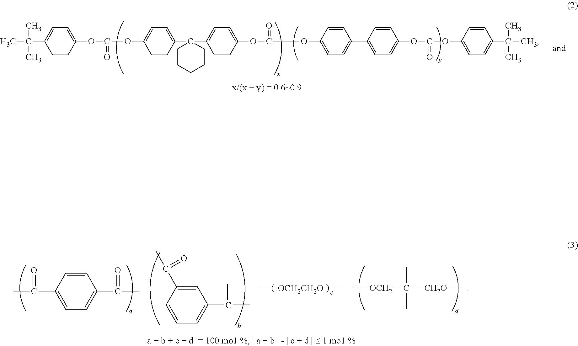
C00016
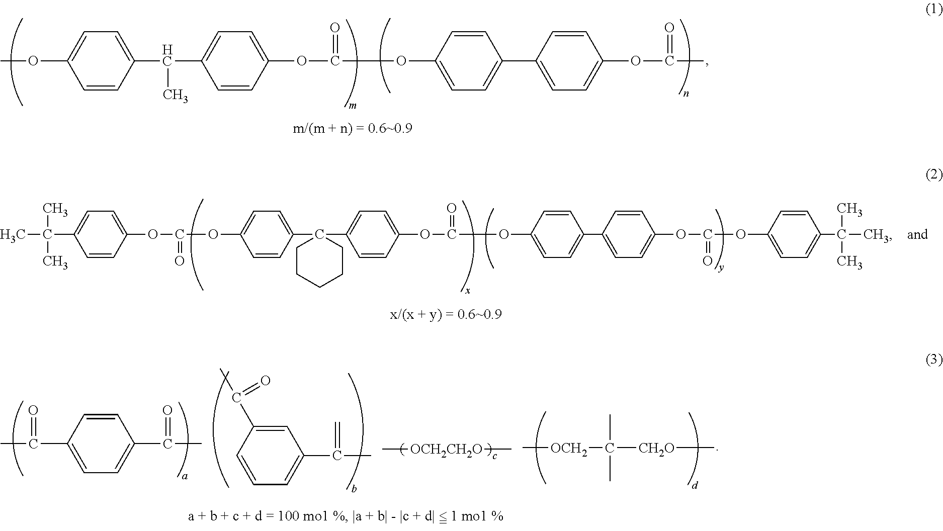
C00017
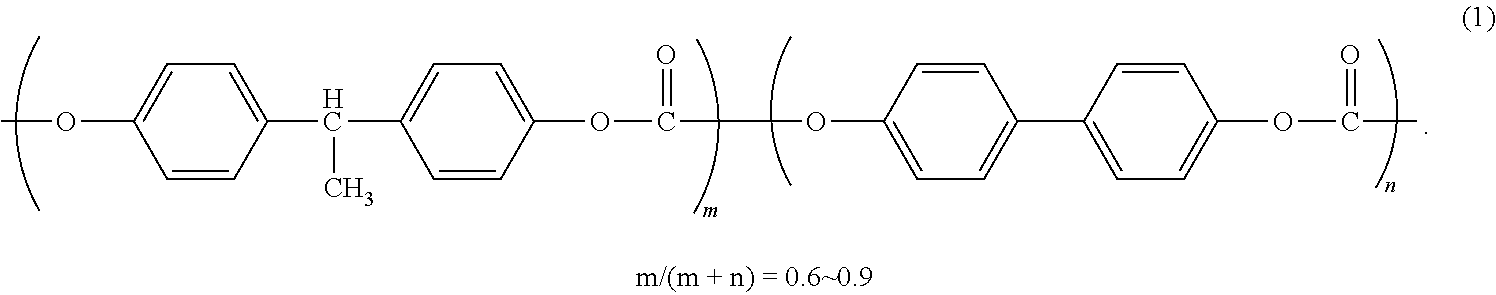
C00018

C00019
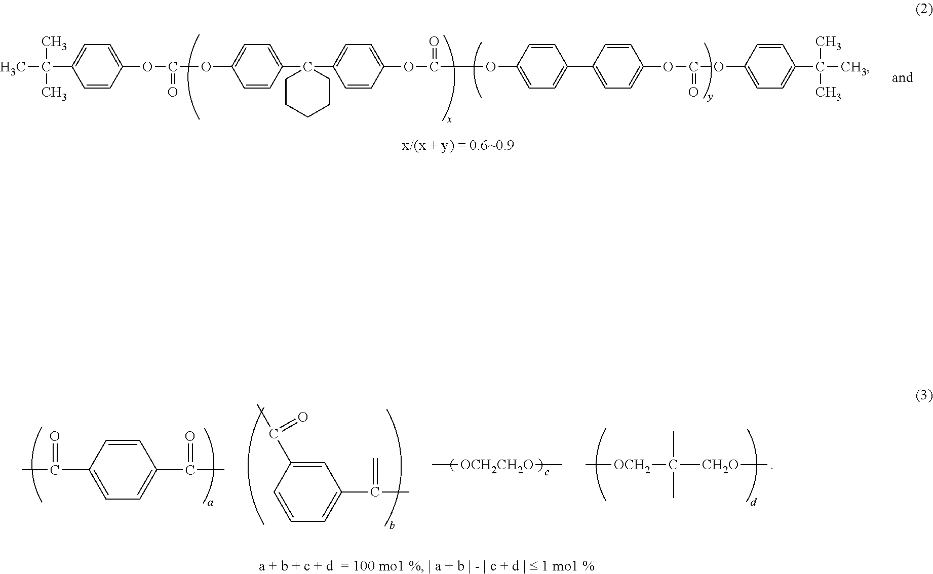
C00020

D00000

D00001

D00002

D00003
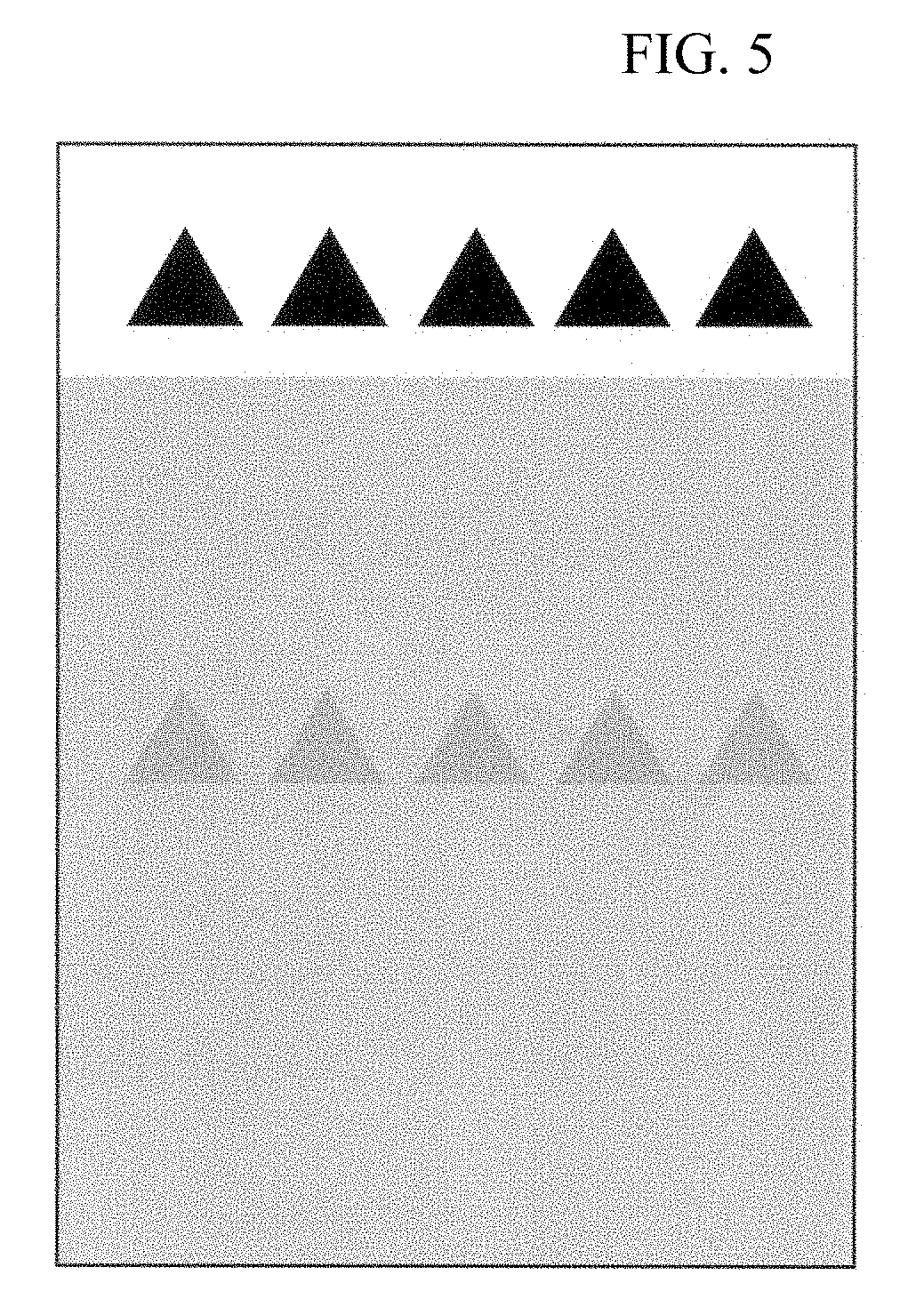
XML
uspto.report is an independent third-party trademark research tool that is not affiliated, endorsed, or sponsored by the United States Patent and Trademark Office (USPTO) or any other governmental organization. The information provided by uspto.report is based on publicly available data at the time of writing and is intended for informational purposes only.
While we strive to provide accurate and up-to-date information, we do not guarantee the accuracy, completeness, reliability, or suitability of the information displayed on this site. The use of this site is at your own risk. Any reliance you place on such information is therefore strictly at your own risk.
All official trademark data, including owner information, should be verified by visiting the official USPTO website at www.uspto.gov. This site is not intended to replace professional legal advice and should not be used as a substitute for consulting with a legal professional who is knowledgeable about trademark law.