Luminaire with controllable light emission
Girotto , et al. Sept
U.S. patent number 10,416,377 [Application Number 15/450,578] was granted by the patent office on 2019-09-17 for luminaire with controllable light emission. This patent grant is currently assigned to Cree, Inc.. The grantee listed for this patent is Cree, Inc.. Invention is credited to Randall Levy Bernard, Ethan Creasman, William L. Dungan, Claudio Girotto, James Ibbetson, Bernd Keller, Theodore D. Lowes, Nathan Ray Snell, Eric Tarsa, Mark Youmans.


View All Diagrams
| United States Patent | 10,416,377 |
| Girotto , et al. | September 17, 2019 |
Luminaire with controllable light emission
Abstract
A luminaire includes a first waveguide having a first primary light emitting surface directed in a first direction and a first secondary light emitting surface directed in a second direction. A second waveguide having a second primary light emitting surface directed in the second direction and a second secondary light emitting surface directed in the first direction. A first plurality of LEDs are optically coupled to the first waveguide and a second plurality of LEDs are optically coupled to the second waveguide. The first and second waveguides are independently operable. The first and second plurality of LEDs may comprise LED groups where each of the LED groups are independently controllable. The light emission pattern and light properties of the emitted light are controllable.
| Inventors: | Girotto; Claudio (Santa Barbara, CA), Tarsa; Eric (Goleta, CA), Snell; Nathan Ray (Raleigh, NC), Ibbetson; James (Santa Barbara, CA), Youmans; Mark (Goleta, CA), Lowes; Theodore D. (Lompoc, CA), Keller; Bernd (Santa Barbara, CA), Creasman; Ethan (Raleigh, NC), Bernard; Randall Levy (Cary, NC), Dungan; William L. (Cary, NC) | ||||||||||
|---|---|---|---|---|---|---|---|---|---|---|---|
| Applicant: |
|
||||||||||
| Assignee: | Cree, Inc. (Durham,
NC) |
||||||||||
| Family ID: | 60243428 | ||||||||||
| Appl. No.: | 15/450,578 | ||||||||||
| Filed: | March 6, 2017 |
Prior Publication Data
| Document Identifier | Publication Date | |
|---|---|---|
| US 20170322364 A1 | Nov 9, 2017 | |
Related U.S. Patent Documents
| Application Number | Filing Date | Patent Number | Issue Date | ||
|---|---|---|---|---|---|
| 62333000 | May 6, 2016 | ||||
| Current U.S. Class: | 1/1 |
| Current CPC Class: | G02B 6/122 (20130101); F21V 23/0435 (20130101); G02B 6/0076 (20130101); G02B 6/12004 (20130101); F21S 6/005 (20130101); G02B 6/0045 (20130101); F21V 23/0464 (20130101); G02B 6/0088 (20130101); F21V 23/0485 (20130101); G02B 6/0063 (20130101); F21V 23/0471 (20130101); F21Y 2115/10 (20160801); G02B 6/0068 (20130101); G02B 2006/12083 (20130101); G02B 6/0078 (20130101); G02B 6/0073 (20130101) |
| Current International Class: | F21V 8/00 (20060101); F21V 23/04 (20060101); G02B 6/12 (20060101); G02B 6/122 (20060101); F21S 6/00 (20060101) |
References Cited [Referenced By]
U.S. Patent Documents
| 615108 | November 1898 | De Segundo |
| 766515 | August 1904 | Northrup et al. |
| D67806 | July 1925 | Hoyt et al. |
| 2043951 | June 1936 | Eksergian et al. |
| 2992587 | July 1961 | Hicks, Jr. et al. |
| 3372740 | March 1968 | Kastovich et al. |
| 3532871 | October 1970 | Shipman |
| D219546 | December 1970 | Kaiser et al. |
| 4146297 | March 1979 | Alferness et al. |
| 4441787 | April 1984 | Lichtenberger |
| 4714983 | December 1987 | Lang et al. |
| D298861 | December 1988 | Ewing et al. |
| 4914553 | April 1990 | Hamada et al. |
| 4954930 | September 1990 | Maegawa et al. |
| 4977486 | December 1990 | Gotoh et al. |
| 5005108 | April 1991 | Pristash et al. |
| 5009483 | April 1991 | Rockwell, III et al. |
| 5026161 | June 1991 | Werner |
| 5040098 | August 1991 | Tanaka et al. |
| 5047761 | September 1991 | Sell et al. |
| 5061404 | October 1991 | Wu et al. |
| 5097258 | March 1992 | Iwaki |
| 5113177 | May 1992 | Cohen et al. |
| 5113472 | May 1992 | Gualtieri et al. |
| 5171080 | December 1992 | Bathurst |
| 5175787 | December 1992 | Gualtieri et al. |
| 5186865 | February 1993 | Wu et al. |
| 5245689 | September 1993 | Gualtieri |
| 5253317 | October 1993 | Allen et al. |
| 5295019 | March 1994 | Rapoport et al. |
| 5309544 | May 1994 | Saxe et al. |
| 5359687 | October 1994 | McFarland et al. |
| 5359691 | October 1994 | Tai et al. |
| 5396350 | March 1995 | Beeson et al. |
| 5398179 | March 1995 | Pacheco et al. |
| 5400224 | March 1995 | Dunah et al. |
| 5428468 | June 1995 | Zimmerman et al. |
| 5461547 | October 1995 | Ciupke et al. |
| 5462700 | October 1995 | Beeson et al. |
| 5481385 | January 1996 | Zimmerman et al. |
| 5506924 | April 1996 | Inoue et al. |
| 5521725 | May 1996 | Beeson et al. |
| 5521726 | May 1996 | Zimmerman et al. |
| 5528720 | June 1996 | Winston et al. |
| 5537304 | July 1996 | Klaus et al. |
| 5541039 | July 1996 | McFarland et al. |
| 5548670 | August 1996 | Koike et al. |
| 5553092 | September 1996 | Bruce et al. |
| 5555109 | September 1996 | Zimmerman et al. |
| 5555160 | September 1996 | Tawara et al. |
| 5555329 | September 1996 | Kuper et al. |
| 5572411 | November 1996 | Watai et al. |
| 5577492 | November 1996 | Parkyn, Jr. et al. |
| 5584556 | December 1996 | Yokoyama et al. |
| 5598280 | January 1997 | Nishio et al. |
| 5598281 | January 1997 | Zimmerman et al. |
| 5613751 | March 1997 | Parker et al. |
| 5613770 | March 1997 | Chin, Jr. et al. |
| 5624202 | April 1997 | Grierson |
| 5657408 | August 1997 | Ferm et al. |
| 5658066 | August 1997 | Hirsch et al. |
| 5659410 | August 1997 | Koike et al. |
| 5676453 | October 1997 | Parkyn, Jr. et al. |
| 5676457 | October 1997 | Simon |
| 5677702 | October 1997 | Inoue et al. |
| 5685634 | November 1997 | Mulligan et al. |
| 5696865 | December 1997 | Beeson et al. |
| 5702176 | December 1997 | Engle et al. |
| 5718497 | February 1998 | Yokoyama et al. |
| 5727107 | March 1998 | Umemoto et al. |
| 5735590 | April 1998 | Kashima et al. |
| 5739931 | April 1998 | Zimmerman et al. |
| 5748828 | May 1998 | Steiner et al. |
| 5761355 | June 1998 | Kuper et al. |
| 5769522 | June 1998 | Kaneko et al. |
| 5771039 | June 1998 | Ditzik et al. |
| 5777857 | July 1998 | Degelmann et al. |
| 5806955 | September 1998 | Parkyn, Jr. et al. |
| 5812714 | September 1998 | Hulse et al. |
| 5818555 | October 1998 | Yokoyama et al. |
| 5839823 | November 1998 | Hou et al. |
| 5850498 | December 1998 | Shacklette et al. |
| 5854872 | December 1998 | Tai et al. |
| 5863113 | January 1999 | Oe et al. |
| 5872883 | February 1999 | Ohba et al. |
| 5897201 | April 1999 | Simon et al. |
| 5914759 | June 1999 | Higuchi et al. |
| 5914760 | June 1999 | Daiku |
| 5949933 | September 1999 | Steiner et al. |
| 5961198 | October 1999 | Hira et al. |
| 5967637 | October 1999 | Ishikawa et al. |
| 5974214 | October 1999 | Shacklette et al. |
| 5997148 | December 1999 | Ohkawa et al. |
| 5999281 | December 1999 | Abbott et al. |
| 5999685 | December 1999 | Goto et al. |
| 6002079 | December 1999 | Shin et al. |
| 6002829 | December 1999 | Winston et al. |
| 6007209 | December 1999 | Pelka et al. |
| 6043951 | March 2000 | Lee |
| 6044196 | March 2000 | Winston et al. |
| 6079838 | June 2000 | Parker et al. |
| 6097549 | August 2000 | Jenkins et al. |
| 6134092 | October 2000 | Pelka et al. |
| 6139163 | October 2000 | Satoh et al. |
| 6139176 | October 2000 | Hulse et al. |
| 6151089 | November 2000 | Yang et al. |
| 6155692 | December 2000 | Ohkawa et al. |
| 6155693 | December 2000 | Spiegel et al. |
| 6161939 | December 2000 | Bansbach et al. |
| 6164790 | December 2000 | Lee |
| 6164791 | December 2000 | Gwo-Juh et al. |
| 6167182 | December 2000 | Shinohara et al. |
| 6185357 | February 2001 | Zou et al. |
| 6206535 | March 2001 | Hattori et al. |
| 6231200 | May 2001 | Shinohara et al. |
| 6232592 | May 2001 | Sugiyama |
| 6241363 | June 2001 | Lee |
| 6257737 | July 2001 | Marshall et al. |
| 6259854 | July 2001 | Shinji et al. |
| 6304693 | October 2001 | Buelow, II et al. |
| 6310704 | October 2001 | Dogan et al. |
| 6318880 | November 2001 | Siminovitch |
| 6379016 | April 2002 | Boyd et al. |
| 6379017 | April 2002 | Nakabayashi et al. |
| 6400086 | June 2002 | Huter |
| 6421103 | July 2002 | Yamaguchi |
| 6443594 | September 2002 | Marshall et al. |
| 6461007 | October 2002 | Akaoka |
| 6473554 | October 2002 | Pelka et al. |
| 6480307 | November 2002 | Yang |
| 6485157 | November 2002 | Ohkawa |
| 6508563 | January 2003 | Parker et al. |
| 6523986 | February 2003 | Hoffmann |
| 6536921 | March 2003 | Simon |
| 6541720 | April 2003 | Gerald et al. |
| 6554451 | April 2003 | Keuper |
| 6568819 | May 2003 | Yamazaki et al. |
| 6582103 | June 2003 | Popovich et al. |
| 6585356 | July 2003 | Ohkawa |
| 6598998 | July 2003 | West et al. |
| 6612723 | September 2003 | Futhey et al. |
| 6616290 | September 2003 | Ohkawa |
| 6629764 | October 2003 | Uehara |
| 6633722 | October 2003 | Kohara et al. |
| 6634772 | October 2003 | Yaphe et al. |
| 6637924 | October 2003 | Pelka et al. |
| 6647199 | November 2003 | Pelka et al. |
| 6652109 | November 2003 | Nakamura |
| 6659628 | December 2003 | Gomez Del Campo |
| 6671452 | December 2003 | Winston et al. |
| 6676284 | January 2004 | Wynne Willson |
| 6678021 | January 2004 | Ohkawa |
| 6679621 | January 2004 | West et al. |
| 6712481 | March 2004 | Parker et al. |
| 6724529 | April 2004 | Sinkoff |
| 6724543 | April 2004 | Chinniah et al. |
| 6727965 | April 2004 | Kubota |
| 6752505 | June 2004 | Parker et al. |
| 6755546 | June 2004 | Ohkawa |
| 6755556 | June 2004 | Gasquet et al. |
| 6758582 | July 2004 | Hsiao et al. |
| 6775460 | August 2004 | Steiner et al. |
| 6796676 | September 2004 | Severtson et al. |
| 6802626 | October 2004 | Belfer et al. |
| 6802628 | October 2004 | Kuo |
| 6840656 | January 2005 | Kuo |
| 6845212 | January 2005 | Gardiner et al. |
| 6876408 | April 2005 | Yamaguchi |
| 6894740 | May 2005 | Ohkawa |
| 6896381 | May 2005 | Benitez et al. |
| 6924943 | August 2005 | Minano et al. |
| 6971758 | December 2005 | Inui et al. |
| 6974241 | December 2005 | Hara et al. |
| 6992335 | January 2006 | Ohkawa |
| 7008097 | March 2006 | Hulse |
| 7010212 | March 2006 | Emmons et al. |
| 7021805 | April 2006 | Amano et al. |
| 7025482 | April 2006 | Yamashita et al. |
| 7046318 | May 2006 | Yu et al. |
| 7046905 | May 2006 | Gardiner et al. |
| 7052157 | May 2006 | Lau |
| 7063430 | June 2006 | Greiner |
| 7072096 | July 2006 | Holman et al. |
| 7083313 | August 2006 | Smith |
| 7085460 | August 2006 | Leu et al. |
| 7090370 | August 2006 | Clark et al. |
| 7090389 | August 2006 | Parker et al. |
| 7097341 | August 2006 | Tsai |
| 7106528 | September 2006 | Ohmori et al. |
| 7111969 | September 2006 | Bottesch et al. |
| 7118253 | October 2006 | Simon |
| 7131764 | November 2006 | Hsu et al. |
| 7152985 | December 2006 | Benitez et al. |
| 7160010 | January 2007 | Chinniah et al. |
| 7160015 | January 2007 | Parker |
| 7168841 | January 2007 | Hsieh et al. |
| 7175330 | February 2007 | Chen |
| 7178941 | February 2007 | Roberge et al. |
| 7179946 | February 2007 | Scholz et al. |
| 7182480 | February 2007 | Kan |
| 7192174 | March 2007 | Myoung |
| 7195374 | March 2007 | Saccomanno et al. |
| 7204634 | April 2007 | Chen et al. |
| 7209628 | April 2007 | Winston et al. |
| 7213940 | May 2007 | Van De Ven et al. |
| 7218830 | May 2007 | Iimura |
| 7222995 | May 2007 | Bayat et al. |
| 7223004 | May 2007 | Chen et al. |
| 7246931 | July 2007 | Hsieh et al. |
| 7258467 | August 2007 | Saccomanno et al. |
| 7265800 | September 2007 | Jagt et al. |
| 7273299 | September 2007 | Parkyn et al. |
| 7290906 | November 2007 | Suzuki et al. |
| 7292767 | November 2007 | Cheng |
| 7322733 | January 2008 | Chang et al. |
| 7364342 | April 2008 | Parker et al. |
| 7369918 | May 2008 | Cosgrove |
| 7393124 | July 2008 | Williams |
| 7399108 | July 2008 | Ayabe et al. |
| 7400809 | July 2008 | Erben et al. |
| 7404660 | July 2008 | Parker |
| 7407303 | August 2008 | Wanninger |
| 7422357 | September 2008 | Chang |
| 7455416 | November 2008 | Chen |
| 7458714 | December 2008 | Chang |
| 7465074 | December 2008 | Blumel |
| 7486854 | February 2009 | Van Ostrand et al. |
| 7488093 | February 2009 | Huang et al. |
| 7513672 | April 2009 | Parker |
| 7520650 | April 2009 | Smith |
| 7534013 | May 2009 | Simon |
| 7559672 | July 2009 | Parkyn et al. |
| 7566148 | July 2009 | Noh et al. |
| 7566159 | July 2009 | Oon et al. |
| 7581854 | September 2009 | Ford |
| 7614759 | November 2009 | Negley |
| 7614764 | November 2009 | Williams et al. |
| 7626655 | December 2009 | Yamazaki et al. |
| 7628508 | December 2009 | Kita et al. |
| 7635193 | December 2009 | Chang |
| 7635205 | December 2009 | Yu et al. |
| 7639918 | December 2009 | Sayers et al. |
| 7641363 | January 2010 | Chang et al. |
| 7648256 | January 2010 | Shiratsuchi et al. |
| 7654687 | February 2010 | Tsai et al. |
| 7654719 | February 2010 | Chang |
| 7663804 | February 2010 | Chang |
| 7674018 | March 2010 | Holder et al. |
| 7695165 | April 2010 | Chang |
| 7696531 | April 2010 | Miyao |
| 7703945 | April 2010 | Leung et al. |
| 7703950 | April 2010 | Ewert et al. |
| 7703967 | April 2010 | Parker |
| 7710663 | May 2010 | Barnes et al. |
| 7722224 | May 2010 | Coleman et al. |
| 7722241 | May 2010 | Chang |
| 7724321 | May 2010 | Hsieh et al. |
| 7730967 | June 2010 | Ballantyne et al. |
| 7736019 | June 2010 | Shimada et al. |
| 7736045 | June 2010 | Yamashita et al. |
| 7750982 | July 2010 | Nelson et al. |
| 7753551 | July 2010 | Yaphe et al. |
| 7758227 | July 2010 | Coleman |
| 7760290 | July 2010 | Kang et al. |
| 7762705 | July 2010 | Sakai et al. |
| 7766515 | August 2010 | Condon et al. |
| 7771087 | August 2010 | Wilcox et al. |
| 7775697 | August 2010 | Hirano et al. |
| 7776236 | August 2010 | Shih et al. |
| 7780306 | August 2010 | Hoshi |
| 7784954 | August 2010 | Coleman |
| 7798695 | September 2010 | Parker |
| 7806581 | October 2010 | Lee |
| 7810949 | October 2010 | Chang |
| 7810960 | October 2010 | Soderman et al. |
| 7810968 | October 2010 | Walker et al. |
| 7813131 | October 2010 | Liang |
| 7821982 | October 2010 | Chen et al. |
| 7826698 | November 2010 | Meir et al. |
| 7845826 | December 2010 | Aylward et al. |
| 7850357 | December 2010 | Kim et al. |
| 7857487 | December 2010 | Wu et al. |
| 7857619 | December 2010 | Liu |
| 7866871 | January 2011 | Couzin et al. |
| 7905646 | March 2011 | Adachi et al. |
| 7907804 | March 2011 | Meir et al. |
| 7909496 | March 2011 | Matheson et al. |
| 7914192 | March 2011 | Coleman |
| 7914193 | March 2011 | Peifer et al. |
| 7914196 | March 2011 | Parker et al. |
| 7929816 | April 2011 | Meir et al. |
| 7934851 | May 2011 | Boissevain et al. |
| 7967477 | June 2011 | Bloemen et al. |
| 7969531 | June 2011 | Li et al. |
| 7970246 | June 2011 | Travis et al. |
| 7976204 | July 2011 | Li et al. |
| 7991257 | August 2011 | Coleman |
| 7997784 | August 2011 | Tsai |
| 8002450 | August 2011 | Van Ostrand et al. |
| 8033674 | October 2011 | Coleman et al. |
| 8033706 | October 2011 | Kelly et al. |
| 8038308 | October 2011 | Greiner |
| 8047673 | November 2011 | Santoro |
| 8047696 | November 2011 | Ijzerman et al. |
| 8052316 | November 2011 | Lee |
| 8054409 | November 2011 | Hsieh et al. |
| 8057056 | November 2011 | Zhu et al. |
| 8061877 | November 2011 | Chang |
| 8064743 | November 2011 | Meir et al. |
| 8067884 | November 2011 | Li |
| 8070345 | December 2011 | Zhang et al. |
| 8075157 | December 2011 | Zhang et al. |
| 8087807 | January 2012 | Liu et al. |
| 8092068 | January 2012 | Parker et al. |
| 8096671 | January 2012 | Cronk et al. |
| 8096681 | January 2012 | Fang et al. |
| 8113704 | February 2012 | Bae et al. |
| 8128272 | March 2012 | Fine et al. |
| 8129731 | March 2012 | Vissenberg et al. |
| 8152339 | April 2012 | Morgan |
| 8152352 | April 2012 | Richardson |
| 8162524 | April 2012 | Van Ostrand et al. |
| 8172447 | May 2012 | Meir et al. |
| 8177408 | May 2012 | Coleman |
| 8182128 | May 2012 | Meir et al. |
| 8186847 | May 2012 | Hu et al. |
| 8189973 | May 2012 | Travis et al. |
| 8192051 | June 2012 | Dau et al. |
| 8198109 | June 2012 | Lerman et al. |
| 8210716 | July 2012 | Lerman et al. |
| 8212263 | July 2012 | Bierhuizen et al. |
| 8218920 | July 2012 | Van Ostrand et al. |
| 8220955 | July 2012 | Kwak et al. |
| 8220980 | July 2012 | Gingrich, III |
| 8226287 | July 2012 | Teng et al. |
| 8231256 | July 2012 | Coleman et al. |
| 8231258 | July 2012 | Kim et al. |
| 8231259 | July 2012 | Keller et al. |
| 8242518 | August 2012 | Lerman et al. |
| 8246187 | August 2012 | Cheong et al. |
| 8246197 | August 2012 | Huang |
| 8249408 | August 2012 | Coleman |
| 8258524 | September 2012 | Tan et al. |
| 8272756 | September 2012 | Patrick |
| 8272770 | September 2012 | Richardson |
| 8277106 | October 2012 | Van Gorkom et al. |
| 8282261 | October 2012 | Pance et al. |
| 8282853 | October 2012 | Mori et al. |
| 8283354 | October 2012 | Wilson et al. |
| 8283853 | October 2012 | Yan et al. |
| 8287152 | October 2012 | Gill |
| 8292467 | October 2012 | Vissenberg et al. |
| 8297786 | October 2012 | Shani et al. |
| 8297801 | October 2012 | Coushaine et al. |
| 8297818 | October 2012 | Richardson |
| 8301002 | October 2012 | Shani |
| 8310158 | November 2012 | Coplin et al. |
| 8314566 | November 2012 | Steele et al. |
| 8317363 | November 2012 | Zheng |
| 8317366 | November 2012 | Dalton et al. |
| 8319130 | November 2012 | Lee et al. |
| 8328403 | December 2012 | Morgan et al. |
| 8328406 | December 2012 | Zimmermann |
| 8331746 | December 2012 | Bogner et al. |
| 8338199 | December 2012 | Lerman et al. |
| 8338839 | December 2012 | Lerman et al. |
| 8338840 | December 2012 | Lerman et al. |
| 8338841 | December 2012 | Lerman et al. |
| 8338842 | December 2012 | Lerman et al. |
| 8344397 | January 2013 | Lerman et al. |
| 8348446 | January 2013 | Nakamura |
| 8348489 | January 2013 | Holman et al. |
| 8351744 | January 2013 | Travis et al. |
| 8353606 | January 2013 | Jeong |
| 8369678 | February 2013 | Chakmakjian et al. |
| 8371735 | February 2013 | Chen et al. |
| 8376582 | February 2013 | Catone et al. |
| 8382354 | February 2013 | Kim et al. |
| 8382387 | February 2013 | Sandoval |
| 8388173 | March 2013 | Sloan et al. |
| 8388190 | March 2013 | Li et al. |
| 8398259 | March 2013 | Kwak et al. |
| 8398262 | March 2013 | Sloan et al. |
| 8408737 | April 2013 | Wright et al. |
| 8410726 | April 2013 | Dau et al. |
| 8412010 | April 2013 | Ghosh et al. |
| 8414154 | April 2013 | Dau et al. |
| 8419224 | April 2013 | Wan-Chih et al. |
| 8430536 | April 2013 | Zhao |
| 8430548 | April 2013 | Kelly et al. |
| 8432628 | April 2013 | Shiau et al. |
| 8434892 | May 2013 | Zwak et al. |
| 8434893 | May 2013 | Boyer et al. |
| 8434913 | May 2013 | Vissenberg |
| 8434914 | May 2013 | Li et al. |
| 8449128 | May 2013 | Ko et al. |
| 8449142 | May 2013 | Martin et al. |
| 8454218 | June 2013 | Wang et al. |
| 8461602 | June 2013 | Lerman et al. |
| 8469559 | June 2013 | Williams |
| 8475010 | July 2013 | Vissenberg et al. |
| 8482186 | July 2013 | Wang et al. |
| 8485684 | July 2013 | Lou et al. |
| 8506112 | August 2013 | Dau et al. |
| 8511868 | August 2013 | Haugaard et al. |
| 8534896 | September 2013 | Boonekamp |
| 8534901 | September 2013 | Panagotacos et al. |
| 8541795 | September 2013 | Keller et al. |
| 8547022 | October 2013 | Summerford et al. |
| 8564004 | October 2013 | Tarsa et al. |
| 8567983 | October 2013 | Boyer et al. |
| 8567986 | October 2013 | Szprengiel et al. |
| 8573823 | November 2013 | Dau et al. |
| 8585253 | November 2013 | Duong et al. |
| 8591072 | November 2013 | Shani et al. |
| 8591090 | November 2013 | Lin |
| 8593070 | November 2013 | Wang et al. |
| D695431 | December 2013 | Lay |
| 8598778 | December 2013 | Allen et al. |
| 8602586 | December 2013 | Dau et al. |
| 8608351 | December 2013 | Peifer |
| 8616746 | December 2013 | Shinohara |
| 8618735 | December 2013 | Coplin et al. |
| 8632214 | January 2014 | Tickner et al. |
| 8641219 | February 2014 | Johnson et al. |
| 8657479 | February 2014 | Morgan et al. |
| D702377 | April 2014 | Lay |
| 8696173 | April 2014 | Urtiga et al. |
| 8702281 | April 2014 | Okada et al. |
| 8724052 | May 2014 | Hsieh et al. |
| 8736186 | May 2014 | Chobot |
| 8740440 | June 2014 | Mizuno et al. |
| 8755005 | June 2014 | Bierhuizen et al. |
| 8770821 | July 2014 | Ijzerman et al. |
| 8780299 | July 2014 | Ryu et al. |
| 8829821 | September 2014 | Chobot et al. |
| 8833996 | September 2014 | Dau et al. |
| 8833999 | September 2014 | Wang et al. |
| 8840276 | September 2014 | Shani et al. |
| 8851712 | October 2014 | Shani et al. |
| 8864360 | October 2014 | Parker |
| 8870430 | October 2014 | Kamikatano et al. |
| 8870431 | October 2014 | Lin et al. |
| 8882323 | November 2014 | Solomon et al. |
| 8905569 | December 2014 | Thomas et al. |
| 8912735 | December 2014 | Chobot et al. |
| 8915611 | December 2014 | Zhang |
| 8917962 | December 2014 | Nichol et al. |
| 8950919 | February 2015 | Chen |
| 8960969 | February 2015 | Freund |
| 8975827 | March 2015 | Chobot et al. |
| 9046225 | June 2015 | Meyers et al. |
| 9081125 | July 2015 | Dau et al. |
| 9097824 | August 2015 | Vissenberg |
| 9155165 | October 2015 | Chobot |
| 9155166 | October 2015 | Chobot |
| 9303823 | April 2016 | Hu et al. |
| 9433061 | August 2016 | Chobot |
| 9572226 | February 2017 | Motley et al. |
| 2001/0019479 | September 2001 | Nakabayashi et al. |
| 2002/0061178 | May 2002 | Winston et al. |
| 2002/0172039 | November 2002 | Inditsky |
| 2003/0034985 | February 2003 | Needham Riddle et al. |
| 2003/0146688 | August 2003 | Kitazawa et al. |
| 2004/0008952 | January 2004 | Kragl |
| 2004/0080938 | April 2004 | Holman et al. |
| 2004/0135933 | July 2004 | Leu et al. |
| 2004/0146241 | July 2004 | Deladurantaye et al. |
| 2004/0213003 | October 2004 | Lauderdale et al. |
| 2004/0240217 | December 2004 | Rice |
| 2005/0024744 | February 2005 | Falicoff et al. |
| 2005/0111235 | May 2005 | Suzuki et al. |
| 2005/0140848 | June 2005 | Yoo et al. |
| 2005/0201103 | September 2005 | Saccomanno et al. |
| 2005/0210643 | September 2005 | Mezei et al. |
| 2005/0286251 | December 2005 | Smith |
| 2006/0002146 | January 2006 | Baba |
| 2006/0072203 | April 2006 | Lee |
| 2006/0076568 | April 2006 | Keller et al. |
| 2006/0147151 | July 2006 | Wanninger et al. |
| 2006/0187651 | August 2006 | Kim et al. |
| 2006/0262521 | November 2006 | Piepgras et al. |
| 2007/0081780 | April 2007 | Scholl |
| 2007/0086179 | April 2007 | Chen et al. |
| 2007/0121340 | May 2007 | Hoshi |
| 2007/0139905 | June 2007 | Birman et al. |
| 2007/0139965 | June 2007 | Liao |
| 2007/0189033 | August 2007 | Watanabe et al. |
| 2007/0223247 | September 2007 | Lee et al. |
| 2007/0245607 | October 2007 | Awai et al. |
| 2007/0253058 | November 2007 | Wood |
| 2007/0274654 | November 2007 | Choudhury et al. |
| 2007/0279933 | December 2007 | Shiau et al. |
| 2008/0002399 | January 2008 | Villard et al. |
| 2008/0030650 | February 2008 | Kitagawa et al. |
| 2008/0037284 | February 2008 | Rudisill |
| 2008/0094853 | April 2008 | Kim et al. |
| 2008/0137695 | June 2008 | Takahashi et al. |
| 2008/0186273 | August 2008 | Krijn et al. |
| 2008/0192458 | August 2008 | Li |
| 2008/0199143 | August 2008 | Turner |
| 2008/0211990 | September 2008 | Sakai |
| 2008/0232135 | September 2008 | Kinder et al. |
| 2008/0266879 | October 2008 | Chang |
| 2008/0266901 | October 2008 | Chang |
| 2008/0285310 | October 2008 | Aylward et al. |
| 2008/0285304 | November 2008 | Rankin, Jr. et al. |
| 2009/0027893 | January 2009 | Chang |
| 2009/0091948 | April 2009 | Wang et al. |
| 2009/0103293 | April 2009 | Harbers et al. |
| 2009/0175050 | July 2009 | Marttila et al. |
| 2009/0196071 | August 2009 | Matheson et al. |
| 2009/0257242 | October 2009 | Wendman |
| 2009/0297090 | December 2009 | Bogner et al. |
| 2009/0309494 | December 2009 | Patterson et al. |
| 2009/0310367 | December 2009 | Kuo |
| 2009/0316414 | December 2009 | Yang et al. |
| 2010/0008088 | January 2010 | Koizumi et al. |
| 2010/0008628 | January 2010 | Shani |
| 2010/0027257 | February 2010 | Boonekamp et al. |
| 2010/0046219 | February 2010 | Pijlman et al. |
| 2010/0053959 | March 2010 | Ijzerman et al. |
| 2010/0073597 | March 2010 | Bierhuizen et al. |
| 2010/0073911 | March 2010 | Ohkawa |
| 2010/0079843 | April 2010 | Derichs et al. |
| 2010/0079980 | April 2010 | Sakai |
| 2010/0110673 | May 2010 | Bergman et al. |
| 2010/0110679 | May 2010 | Teng et al. |
| 2010/0118531 | May 2010 | Montagne |
| 2010/0128483 | May 2010 | Reo et al. |
| 2010/0133422 | June 2010 | Lin et al. |
| 2010/0157577 | June 2010 | Montgomery et al. |
| 2010/0208460 | August 2010 | Ladewig et al. |
| 2010/0220484 | September 2010 | Shani et al. |
| 2010/0220497 | September 2010 | Ngai |
| 2010/0231143 | September 2010 | May et al. |
| 2010/0238645 | September 2010 | Bailey |
| 2010/0238671 | September 2010 | Catone et al. |
| 2010/0246158 | September 2010 | Van Gorkom et al. |
| 2010/0253881 | October 2010 | Han et al. |
| 2010/0254129 | October 2010 | Le Toquin et al. |
| 2010/0301360 | December 2010 | van de Ven et al. |
| 2010/0302135 | December 2010 | Larson et al. |
| 2010/0302218 | December 2010 | Bita et al. |
| 2010/0302616 | December 2010 | Bita et al. |
| 2010/0302783 | December 2010 | Shastry et al. |
| 2010/0302803 | December 2010 | Bita et al. |
| 2010/0315833 | December 2010 | Holman et al. |
| 2010/0320904 | December 2010 | Meir |
| 2010/0328936 | December 2010 | Pance et al. |
| 2011/0007505 | January 2011 | Wang |
| 2011/0013397 | January 2011 | Catone et al. |
| 2011/0013420 | January 2011 | Coleman et al. |
| 2011/0013421 | January 2011 | Um |
| 2011/0037388 | February 2011 | Lou et al. |
| 2011/0044022 | February 2011 | Ko et al. |
| 2011/0044582 | February 2011 | Travis et al. |
| 2011/0051457 | March 2011 | Chen |
| 2011/0058372 | March 2011 | Lerman et al. |
| 2011/0063830 | March 2011 | Narendran et al. |
| 2011/0063838 | March 2011 | Dau et al. |
| 2011/0063855 | March 2011 | Vissenberg |
| 2011/0069843 | March 2011 | Cohen et al. |
| 2011/0122616 | May 2011 | Hochstein |
| 2011/0163681 | July 2011 | Dau et al. |
| 2011/0163683 | July 2011 | Steele et al. |
| 2011/0170289 | July 2011 | Allen et al. |
| 2011/0180818 | July 2011 | Lerman et al. |
| 2011/0187273 | August 2011 | Summerford et al. |
| 2011/0193105 | August 2011 | Lerman et al. |
| 2011/0193106 | August 2011 | Lerman et al. |
| 2011/0193114 | August 2011 | Lerman et al. |
| 2011/0195532 | August 2011 | Lerman et al. |
| 2011/0198631 | August 2011 | Lerman et al. |
| 2011/0198632 | August 2011 | Lerman et al. |
| 2011/0199769 | August 2011 | Bretschneider et al. |
| 2011/0204390 | August 2011 | Lerman et al. |
| 2011/0204391 | August 2011 | Lerman et al. |
| 2011/0210861 | September 2011 | Winton et al. |
| 2011/0228527 | September 2011 | Van Gorkom et al. |
| 2011/0233568 | September 2011 | An et al. |
| 2011/0248287 | October 2011 | Yuan et al. |
| 2011/0249467 | October 2011 | Boonekamp |
| 2011/0261570 | October 2011 | Okada et al. |
| 2011/0273079 | November 2011 | Pickard et al. |
| 2011/0273882 | November 2011 | Pickard |
| 2011/0280043 | November 2011 | Van Ostrand et al. |
| 2011/0299807 | December 2011 | Kim et al. |
| 2011/0305018 | December 2011 | Angelini et al. |
| 2011/0305027 | December 2011 | Ham |
| 2011/0317436 | December 2011 | Kuan |
| 2012/0008338 | January 2012 | Ono et al. |
| 2012/0014128 | January 2012 | Lin |
| 2012/0020108 | January 2012 | Chang |
| 2012/0026728 | February 2012 | Lou et al. |
| 2012/0026828 | February 2012 | Fjellstad et al. |
| 2012/0033445 | February 2012 | Desmet et al. |
| 2012/0039073 | February 2012 | Tong |
| 2012/0051041 | March 2012 | Edmond et al. |
| 2012/0057325 | March 2012 | Hikmet |
| 2012/0068615 | March 2012 | Duong et al. |
| 2012/0069575 | March 2012 | Koh et al. |
| 2012/0069579 | March 2012 | Koh et al. |
| 2012/0069595 | March 2012 | Catalano |
| 2012/0075873 | March 2012 | Cooper |
| 2012/0113676 | May 2012 | Van Dijk et al. |
| 2012/0114284 | May 2012 | Ender |
| 2012/0120651 | May 2012 | Peck |
| 2012/0140461 | June 2012 | Pickard |
| 2012/0147624 | June 2012 | Li et al. |
| 2012/0152490 | June 2012 | Wen et al. |
| 2012/0161009 | June 2012 | Kothari et al. |
| 2012/0170266 | July 2012 | Germain et al. |
| 2012/0170316 | July 2012 | Lee et al. |
| 2012/0170318 | July 2012 | Tsai et al. |
| 2012/0182767 | July 2012 | Petcavich et al. |
| 2012/0188774 | July 2012 | Okada |
| 2012/0212957 | August 2012 | Hyun et al. |
| 2012/0230019 | September 2012 | Peifer |
| 2012/0242930 | September 2012 | Ryu et al. |
| 2012/0243259 | September 2012 | Zhou et al. |
| 2012/0250296 | October 2012 | Lu et al. |
| 2012/0250319 | October 2012 | Dau et al. |
| 2012/0257383 | October 2012 | Zhang |
| 2012/0268931 | October 2012 | Lerman et al. |
| 2012/0268932 | October 2012 | Lerman et al. |
| 2012/0287619 | November 2012 | Pickard et al. |
| 2012/0287654 | November 2012 | He et al. |
| 2012/0287668 | November 2012 | Richardson |
| 2012/0287677 | November 2012 | Wheatley et al. |
| 2012/0298181 | November 2012 | Cashion et al. |
| 2012/0307496 | December 2012 | Phillips, III et al. |
| 2012/0320626 | December 2012 | Quilici et al. |
| 2012/0326614 | December 2012 | Tsuji et al. |
| 2013/0003348 | January 2013 | Meir et al. |
| 2013/0003363 | January 2013 | Lu et al. |
| 2013/0003409 | January 2013 | Vissenberg et al. |
| 2013/0010464 | January 2013 | Shuja et al. |
| 2013/0028557 | January 2013 | Lee et al. |
| 2013/0033867 | February 2013 | Coplin et al. |
| 2013/0037838 | February 2013 | Speier et al. |
| 2013/0038219 | February 2013 | Dau et al. |
| 2013/0039050 | February 2013 | Dau et al. |
| 2013/0039090 | February 2013 | Dau et al. |
| 2013/0044480 | February 2013 | Sato et al. |
| 2013/0077298 | March 2013 | Steele et al. |
| 2013/0107518 | May 2013 | Boyer et al. |
| 2013/0107527 | May 2013 | Boyer et al. |
| 2013/0107528 | May 2013 | Boyer et al. |
| 2013/0128593 | May 2013 | Luo |
| 2013/0141937 | June 2013 | Katsuta et al. |
| 2013/0170210 | July 2013 | Athalye |
| 2013/0201715 | August 2013 | Dau et al. |
| 2013/0208461 | August 2013 | Warton et al. |
| 2013/0208495 | August 2013 | Dau et al. |
| 2013/0214300 | August 2013 | Lerman et al. |
| 2013/0215612 | August 2013 | Garcia |
| 2013/0223057 | August 2013 | Gassner et al. |
| 2013/0229804 | September 2013 | Holder et al. |
| 2013/0229810 | September 2013 | Pelka et al. |
| 2013/0250584 | September 2013 | Wang et al. |
| 2013/0279198 | October 2013 | Lin et al. |
| 2013/0294059 | November 2013 | Galluccio et al. |
| 2013/0294063 | November 2013 | Lou et al. |
| 2013/0300310 | November 2013 | Hu |
| 2013/0317784 | November 2013 | Huang et al. |
| 2013/0322116 | December 2013 | Pijlman et al. |
| 2013/0328073 | December 2013 | Lowes et al. |
| 2013/0336001 | December 2013 | Boonekamp |
| 2013/0343045 | December 2013 | Lodhie et al. |
| 2013/0343055 | December 2013 | Eckert et al. |
| 2013/0343079 | December 2013 | Unger et al. |
| 2014/0003041 | January 2014 | Dau et al. |
| 2014/0029257 | January 2014 | Boyer et al. |
| 2014/0036510 | February 2014 | Preston et al. |
| 2014/0043850 | February 2014 | Thompson et al. |
| 2014/0071687 | March 2014 | Tickner et al. |
| 2014/0168955 | June 2014 | Gershaw |
| 2014/0211457 | July 2014 | Tarsa et al. |
| 2014/0211462 | July 2014 | Keller et al. |
| 2014/0211476 | July 2014 | Yuan et al. |
| 2014/0211495 | July 2014 | Yuan et al. |
| 2014/0211496 | July 2014 | Durkee |
| 2014/0211497 | July 2014 | Yuan et al. |
| 2014/0211502 | July 2014 | Keller et al. |
| 2014/0211503 | July 2014 | Tarsa |
| 2014/0211504 | July 2014 | Yuan et al. |
| 2014/0211508 | July 2014 | Yuan et al. |
| 2014/0212090 | July 2014 | Wilcox et al. |
| 2014/0268762 | September 2014 | Raleigh et al. |
| 2014/0268790 | September 2014 | Chobot et al. |
| 2014/0268875 | September 2014 | Durkee |
| 2014/0268879 | September 2014 | Mizuyama et al. |
| 2014/0270672 | September 2014 | Durkee |
| 2014/0286052 | September 2014 | McCollum et al. |
| 2014/0334126 | November 2014 | Speier et al. |
| 2014/0347885 | November 2014 | Wilcox et al. |
| 2014/0355297 | December 2014 | Castillo et al. |
| 2014/0355302 | December 2014 | Wilcox et al. |
| 2015/0003059 | January 2015 | Haitz et al. |
| 2015/0008827 | January 2015 | Carrigan et al. |
| 2015/0008828 | January 2015 | Carrigan et al. |
| 2015/0008831 | January 2015 | Carrigan et al. |
| 2015/0015145 | January 2015 | Carrigan et al. |
| 2015/0048758 | February 2015 | Carrigan et al. |
| 2015/0049511 | February 2015 | Tarsa et al. |
| 2015/0055369 | February 2015 | Tarsa et al. |
| 2015/0055371 | February 2015 | van de Ven et al. |
| 2015/0102729 | April 2015 | Creasman et al. |
| 2015/0109820 | April 2015 | Wilcox et al. |
| 2015/0160396 | June 2015 | Wilcox et al. |
| 2015/0177439 | June 2015 | Durkee et al. |
| 2015/0192742 | July 2015 | Tarsa et al. |
| 2015/0195883 | July 2015 | Harris et al. |
| 2015/0198760 | July 2015 | Wilcox et al. |
| 2015/0204491 | July 2015 | Yuan et al. |
| 2015/0260905 | September 2015 | Yuan et al. |
| 2015/0264780 | September 2015 | Harris et al. |
| 2015/0049507 | October 2015 | Shani et al. |
| 2015/0312983 | October 2015 | Hu et al. |
| 2015/0351187 | December 2015 | McBryde et al. |
| 2017/0205552 | July 2017 | Gierens |
| 10047101 | May 2002 | DE | |||
| 10203106 | Jul 2003 | DE | |||
| 10302563 | Jul 2004 | DE | |||
| 10302564 | Jul 2004 | DE | |||
| 102006009325 | Sep 2007 | DE | |||
| 102006011296 | Sep 2007 | DE | |||
| 102006013343 | Sep 2007 | DE | |||
| 10173870 | Jun 1998 | JP | |||
| 2000147264 | May 2000 | JP | |||
| 3093080 | Apr 2003 | JP | |||
| 2004227934 | Aug 2004 | JP | |||
| 2006131444 | May 2006 | JP | |||
| 2006221922 | Aug 2006 | JP | |||
| 2007123130 | May 2007 | JP | |||
| 9621122 | Jul 1996 | WO | |||
| 9621884 | Jul 1996 | WO | |||
| 9904531 | Jan 1999 | WO | |||
| 0102772 | Jan 2001 | WO | |||
| 03031869 | Apr 2003 | WO | |||
| WO 2004005983 | Jan 2004 | WO | |||
| 2008152561 | Dec 2008 | WO | |||
| 2009012484 | Jan 2009 | WO | |||
| 2011130648 | Oct 2011 | WO | |||
| 2013078463 | May 2013 | WO | |||
| 2013082537 | Jun 2013 | WO | |||
| 2014120672 | Aug 2014 | WO | |||
| 2014120672 | Aug 2014 | WO | |||
| 2014120968 | Aug 2014 | WO | |||
| 2014145283 | Sep 2014 | WO | |||
| WO 2015028328 | Mar 2015 | WO | |||
Other References
|
Ebner/Block et al, Apr. 2018. cited by examiner . U.S. Appl. No. 14/472,064, Office Action, dated Mar. 9, 2018. cited by applicant . U.S. Appl. No. 62/292,528, filed Feb. 8, 2016. cited by applicant . IPRP for International Application No. PCT/US2014/028938, dated Sep. 24, 2015, Applicant, Cree, Inc., (12 pages). cited by applicant . Non-final Office action dated Jul. 31, 2015, for U.S. Appl. No. 14/015,801, Applicant, Cree, Inc. (48 pages). cited by applicant . Non-final Office action dated Jun. 10, 2015, for U.S. Appl. No. 13/842,521, Applicant, Cree, Inc. (53 pages). cited by applicant . Non-final Office action dated Apr. 1, 2015, for U.S. Appl. No. 13/841,074, Applicant, Cree, Inc. (57 pages). cited by applicant . Final Office action dated Jun. 2, 2015, for U.S. Appl. No. 13/841,622, Applicant, Cree, Inc. (58 pages). cited by applicant . Non-final Office action dated Mar. 24, 2015, for U.S. Appl. No. 13/840,563, Applicant, Cree, Inc. (36 pages). cited by applicant . Final Office action dated Jun. 11, 2015, for U.S. Appl. No. 13/938,877, Applicant, Cree, Inc. (40 pages). cited by applicant . Non-final Office action dated Apr. 30, 2015, for U.S. Appl. No. 14/101,132, Applicant, Cree, Inc. (21 pages). cited by applicant . Non-final Office action dated Aug. 12, 2015, for U.S. Appl. No. 14/577,730, Applicant, Cree, Inc. (52 pages). cited by applicant . Non-final Office action dated May 20, 2015, for U.S. Appl. No. 14/101,051, Applicant, Cree, Inc. (17 pages). cited by applicant . Non-final Office action dated Feb. 27, 2015, for U.S. Appl. No. 14/292,778, Applicant, Cree, Inc. (10 pages). cited by applicant . Non-final Office action dated Sep. 4, 2015, for U.S. Appl. No. 14/101,132, Applicant, Cree, Inc. (48 pages). cited by applicant . Non-final Office action dated Aug. 31, 2015, for U.S. Appl. No. 14/292,778, Applicant, Cree, Inc. (49 pages). cited by applicant . Invitation to Pay Additional Fees for International Application No. PCT/US2015/032011 dated Aug. 6, 2015, Applicant, Cree, Inc. (2 pages). cited by applicant . Invitation to Pay Additional Fees for International Application No. PCT/US2015/020601 dated Jun. 5, 2015, Applicant, Cree, Inc. (2 pages). cited by applicant . Non-final Office action dated Jun. 30, 2015, for U.S. Appl. No. 14/583,415, Applicant, Cree, Inc. (216 pages). cited by applicant . U.S. Appl. No. 62/292,528, filed Feb. 8, 2016, (198 pages). cited by applicant . U.S. Appl. No. 15/587,442, filed May 5, 2017, (89 pages). cited by applicant . Iijima et al., "Document Scanner Using Polymer Waveguides With a Microlens Array," Optical Engineering, vol. 41, Issue 11, pp. 2743-2748, Oct. 28, 2002 (4 pages). cited by applicant . Ji et al., "Electrically Controllable Microlens Array Fabricated by Anisotropic Phase Separation From Liquid-Crystal and Polymer Composite Materials," vol. 28, No. 13, Optics Letters, pp. 1147-1149, Jul. 1, 2003 (4 pages). cited by applicant . Drain, Kieran, "Transformations in Lighting: 2011 DOE Solid-State Lighting R&D Workshop, Panel 3: Novel Lighting Concepts for Large Interior Spaces," PowerPoint presentation printed Nov. 2013 (23 pages). cited by applicant . Web page at http://www.oluce.com/en/lamps/table/colombo-281-detail, printed Nov. 19, 2013 (2 pages). cited by applicant . International Search Report and Written Opinion for International Application No. PCT/US2014/013840, dated Jul. 28, 2014, Applicant, Cree, Inc. (17 pages). cited by applicant . International Search Report and Written Opinion for International Application No. PCT/US14/30017, dated Aug. 1, 2014, Applicant, Cree, Inc., (21 pages). cited by applicant . International Search Report and Written Opinion for International Application No. PCT/US2014/072848, dated Mar. 25, 2015, Applicant, Cree, Inc., (17 pages). cited by applicant . International Search Report and Written Opinion for International Application No. PCT/US2014/013408, dated Jul. 17, 2014, Applicant, Cree, Inc. (21 pages). cited by applicant . IPRP for International Application No. PCT/US2014/013400, dated Sep. 24, 2015, Applicant, Cree, Inc., (14 pages). cited by applicant . International Search Report and Written Opinion dated Jul. 28, 2014, for International Application No. PCT/US2014/28938, Applicant, Cree, Inc. (19 pages). cited by applicant . International Search Report and Written Opinion dated Jul. 24, 2014, for International Application No. PCT/US2014/28887, Applicant, Cree, Inc. (15 pages). cited by applicant . International Search Report and Written Opinion for International Application No. PCT/US2015/020601, dated Jul. 31, 2015, Applicant, Cree, Inc. (23 pages). cited by applicant . European Extended Search Report dated May 19, 2015 for EP Application No. 14192325.0, Applicant, Cree, Inc. (5 pages). cited by applicant . International Search Report and Written Opinion dated Mar. 25, 2015, for International Application No. PCT/US2014/072860, Applicant, Cree, Inc. (14 pages). cited by applicant . International Search Report and Written Opinion for International Application No. PCT/US15/32050, Applicant, Cree, Inc., dated Oct. 19, 2015 (19 pages). cited by applicant . International Search Report and Written Opinion dated Jan. 11, 2016, for International Application No. PCT/US2015/032040, Applicant, Cree, Inc., (16 pages). cited by applicant . USPTO Office Action dated Nov. 13, 2015, for U.S. Appl. No. 13/841,622, Applicant, Cree, Inc. (7 pages). cited by applicant . Web page at http://www.fusionoptix.com/lighting/components/array-optics.htm, printed May 9, 2013 (2 pages). cited by applicant . Invitation to Pay Additional Fees for International Application No. PCT/US2014/013840, dated May 8, 2014, Applicant, Cree, Inc. (2 pages). cited by applicant . Invitation to Pay Additional Fees for International Application No. PCT/US2014/013408, dated May 8, 2014, Applicant, Cree, Inc. (2 pages). cited by applicant . U.S. Appl. No. 13/657,421, filed Oct. 22, 2012 (38 pages). cited by applicant . Invitation to Pay Additional Fees for International Application No. PCT/US2015/032040 dated Aug. 6, 2015, Applicant, Cree, Inc. (2 pages). cited by applicant . U.S. Appl. No. 14/291,829, filed May 30, 2014, Inventors, Yuan et al. (65 pages). cited by applicant . U.S. Appl. No. 14/292,001, filed May 30, 2014, Inventors, Hu et al. (38 pages). cited by applicant . U.S. Appl. No. 14/292,286, filed May 30, 2014, Inventors, McBryde et al. (103 pages). cited by applicant . U.S. Appl. No. 61/932,058, filed Jan. 27, 2014, Inventors, Carrigan et al., (203 pages). cited by applicant . U.S. Appl. No. 14/618,884, filed Feb. 10, 2015, Inventors, Castillo et al. (56 pages). cited by applicant . U.S. Appl. No. 14/462,322, filed Aug. 18, 2014, Inventors, Castillo et al. (31 pages). cited by applicant . U.S. Appl. No. 62/088,375, filed Dec. 5, 2014, Inventors, Hussell et al. (51 pages). cited by applicant . U.S. Appl. No. 14/618,819, filed Feb. 10, 2015, Inventors, Bendtsen et al. (37 pages). cited by applicant . U.S. Appl. No. 14/801,476, filed Jul. 16, 2015, Inventors, de Sugny et al. (38 pages). cited by applicant . U.S. Appl. No. 14/472,078, filed Aug. 28, 2014, Inventors, Tarsa et al. (60 pages). cited by applicant . IPRP for International Application No. PCT/US2014/013840, dated Aug. 13, 2015, Applicant, Cree, Inc. (10 pages). cited by applicant . IPRP for International Application No. PCT/US2014/013891, dated Aug. 13, 2015, Applicant, Cree, Inc., (8 pages). cited by applicant . IPRP for International Application No. PCT/US2014/013934, dated Aug. 13, 2015, Applicant, Cree, Inc., (11 pages). cited by applicant . IPRP for International Application No. PCT/US2014/013854, dated Jun. 5, 2014, Applicant, Cree, Inc., (9 pages). cited by applicant . IPRP for International Application No. PCT/US2014/013931, dated Aug. 13, 2015, Applicant, Cree, Inc., (15 pages). cited by applicant . IPRP for International Application No. PCT/US2014/013408, dated Aug. 13, 2015, Applicant, Cree, Inc., (15 pages). cited by applicant . U.S. Appl. No. 14/839,557, filed Aug. 28, 2015, Inventors, Wilcenski et al. (63 pages). cited by applicant . IPRP for International Application No. PCT/US2014/028887, dated Sep. 24, 2015, Applicant, Cree, Inc., (9 pages). cited by applicant . U.S. Appl. No. 14/472,064, Restriction Requirement, dated Jan. 30, 2017, 6 pages. cited by applicant . U.S. Appl. No. 14/472,064, Office Action, dated Jun. 22, 2017, 18 pages. cited by applicant . U.S. Appl. No. 14/472,064, Final Office Action, dated Oct. 16, 2017. cited by applicant. |
Primary Examiner: Cariaso; Alan B
Attorney, Agent or Firm: Myers Bigel, P.A.
Government Interests
REFERENCE REGARDING FEDERALLY SPONSORED RESEARCH OR DEVELOPMENT
This invention was made with government support under Contract No. DE-EE0007620 awarded by The Department of Energy. The government has certain rights in the invention.
Parent Case Text
This application claims benefit of priority under 35 U.S.C. .sctn. 119(e) to the filing date of U.S. Provisional Application No. 62/333,000, as filed on May 6, 2016, which is incorporated herein by reference in its entirety.
Claims
The invention claimed is:
1. A luminaire comprising: a first waveguide having a first primary light emitting surface directed in a first direction and a first secondary light emitting surface directed in a second direction, and a second waveguide having a second primary light emitting surface directed in the second direction and a second secondary light emitting surface directed in the first direction, the first secondary light emitting surface and the second secondary light emitting surface being disposed adjacent one another such that the first primary light emitting surface and the second primary light emitting surface face generally away from one another, and the first primary light emitting surface comprising a first plurality of light extraction features that emit light in a first light emission pattern and the second primary light emitting surface comprising a second plurality of light extraction features that emit light in a second light emission pattern, the first light emission pattern being different than the second light emission pattern; a first plurality of LEDs being optically coupled to the first waveguide such that activation of the first plurality of LEDs causes light to be emitted from the first primary light emitting surface and a second plurality of LEDs being optically coupled to the second waveguide such that activation of the second plurality of LEDs causes light to be emitted from the second primary light emitting surface, and a controller controlling operation of the first plurality of LEDs and the second plurality of LEDs such that the first plurality of LEDs and the second plurality of LEDs are independently operable.
2. The luminaire of claim 1 wherein the first plurality of LEDs comprises a first plurality of LED groups, wherein the controller controls operation of the first plurality of LED groups such that each one of the first plurality of LED groups is independently controllable.
3. The luminaire of claim 2 wherein the second plurality of LEDs comprises a second plurality of LED groups, wherein the controller controls operation of the second plurality of LED groups such that each one of the second plurality of LED groups is independently controllable.
4. The luminaire of claim 1 wherein the first waveguide comprises a first plurality of waveguide sections and the first plurality of LEDs comprises a first plurality of LED groups, one of the first plurality of LED groups being associated with one of the first plurality of waveguide sections, wherein the controller controls operation of the first plurality of LED groups such that each one of the first plurality of LED groups is independently controllable.
5. The luminaire of claim 4 wherein the second waveguide comprises a second plurality of waveguide sections and the second plurality of LEDs comprises a second plurality of LED groups, one of the second plurality of groups of LEDs being associated with one of the second plurality of waveguide sections, wherein the controller controls operation of the second plurality of LED groups such that each one of the second plurality of LED groups is independently controllable.
6. The luminaire of claim 5 wherein the first plurality of waveguide sections are coextensive with the second plurality of waveguide sections.
7. The luminaire of claim 1 wherein the controller controls the output of the first plurality of LEDs and the second plurality of LEDs based on an input from a detector.
8. The luminaire of claim 7 wherein the detector comprises an ambient light detector for detecting ambient light.
9. The luminaire of claim 8 wherein the controller alters the lux output level of at least one of the first plurality of LEDS and the second plurality of LEDs in response to input from the ambient light detector.
10. The luminaire of claim 7 wherein the detector comprises an occupancy detector for detecting a stimulus adjacent the luminaire.
11. The luminaire of claim 10 wherein the controller alters the lux output level of at least one of the first plurality of LEDs and the second plurality of LEDs in response to input from the occupancy detector.
12. The luminaire of claim 1 wherein the controller controls the output of the first plurality of LEDs and the second plurality of LEDs based on an input from a user control.
13. The luminaire of claim 12 wherein the user control comprises a capacitive sensor.
14. The luminaire of claim 13 wherein the capacitive sensor independently controls the on/off state and dimming levels of at least one of the first plurality of LEDs and the second plurality of LEDs.
15. The luminaire of claim 12 wherein the user control comprises a remote control that communicates with the controller over a wireless connection.
16. The luminaire of claim 5 wherein the first plurality of waveguide sections are coplanar and the second plurality of waveguide sections are coplanar.
17. The luminaire of claim 3 wherein independent energization of the first plurality of LED groups and the second plurality of LED groups generates a directional light pattern, the directional light pattern being variable along an axis of orientation of the first waveguide and the second waveguide and in a plane perpendicular to the axis of orientation.
18. The luminaire of claim 1 wherein the first waveguide and the second waveguide are supported on a support structure such that the primary light emitting surfaces are disposed horizontally.
19. A luminaire comprising: a plurality of first waveguide sections, each of the plurality of first waveguide sections having a first primary light emitting surface directed in a first direction and a first secondary light emitting surface directed in a second direction and a plurality of second waveguide sections, each of the plurality of second waveguide sections having a second primary light emitting surface directed in the second direction and a second secondary light emitting surface directed in the first direction, the first secondary light emitting surfaces and the second secondary light emitting surfaces being disposed adjacent one another such that light is primarily emitted from the luminaire through at least one of the first primary light emitting surface and second primary light emitting surface; at least one first LED being optically coupled to each of the first waveguide sections and at least one second LED being optically coupled to each of the second waveguide sections, and a controller controlling operation of the at least one first LED and the at least one second LED such that each of the at least one first LED and the at least one second LED are independently operable.
20. The luminaire of claim 19 wherein the first waveguide sections are in a one-to-one relationship with the second waveguide sections.
21. The luminaire of claim 19 comprising: a support structure being supportable on a surface, the support structure supporting the plurality of first waveguide sections and the plurality of second waveguide sections; each of the at least one first LED and the at least one second LED being operable to emit light from the waveguide having a light emission pattern and at least one light property, the controller controlling operation of the at least one first LED and the at least one second LED such that the light emission pattern and the at least one light property of the emitted light are controllable.
22. The luminaire of claim 21 wherein the at least one light property comprises at least one of color, color temperature, brightness, CRI, and color gamut.
23. The luminaire of claim 21 wherein the light emission pattern comprises light emitted at least in one of an axial direction and a lateral direction.
Description
FIELD OF DISCLOSURE
The present subject matter relates to lighting devices, and more particularly, to a luminaire incorporating waveguides for general illumination.
BACKGROUND
An optical waveguide mixes and directs light emitted by one or more light sources, such as one or more light emitting diodes (LEDs). A typical optical waveguide includes three main components: one or more coupling elements, one or more distribution elements, and one or more extraction elements. The coupling elements(s) direct light into the distribution element(s) and condition the light to interact with the subsequent components. The one or more distribution elements control how light flows through the waveguide and is dependent on the waveguide geometry and material. The extraction element(s) determine how light is emitted by controlling where and in what direction the light exits the waveguide.
After light has been coupled into the waveguide, it is guided and conditioned to the locations of extraction. In accordance with well-known principles of total internal reflectance the light rays continue to travel through the waveguide until such rays strike a light extraction surface and the light rays escape the waveguide. By appropriately shaping the waveguide surfaces, the position from which light is emitted and the angular distribution of the emitted light may be controlled. The design of the coupling elements, the distribution elements and the extraction devices provide control over the appearance of the waveguide, its resulting distribution of emitted light, and system optical efficiency.
SUMMARY
In one embodiment a luminaire comprises a first waveguide having a first primary light emitting surface directed in a first direction and a first secondary light emitting surface directed in a second direction, and a second waveguide having a second primary light emitting surface directed in the second direction and a second secondary light emitting surface directed in the first direction. The first secondary light emitting surface and the second secondary light emitting surface are disposed adjacent one another. At least one first LED is optically coupled to the first waveguide such that activation of the first LED(s) causes light to be emitted from the first primary light emitting surface and at least one second LED is optically coupled to the second waveguide such that activation of the second LED(s) causes light to be emitted from the second primary light emitting surface. The first LED(s) and the second LED(s) are independently operable.
The first LED(s) may comprise a first plurality of LED groups where each of the first plurality of LED groups may be independently controllable. The second LED(s) may comprise a second plurality of LED groups where each of the second plurality of LED groups may be independently controllable. The first waveguide may comprise a first plurality of waveguide sections where one of the first plurality of LED groups is associated with one of the first plurality of waveguide sections and each of the first plurality of LEDs groups may be independently controllable. The second waveguide may comprise a second plurality of waveguide sections where one of the second plurality of LED groups is associated with one of the second plurality of waveguide sections and each of the second plurality of LED groups may be independently controllable. The first plurality of waveguide sections may be coextensive with the second plurality of waveguide sections. A controller may control the output of the first LED(s) and the second LED(s) based on an input from a detector. The detector may comprise an ambient light detector for detecting ambient light. The controller may alter the lux output level of the first LED(s) and the second LED(s) in response to input from the ambient light detector. The detector may comprise an occupancy detector for detecting a stimulus adjacent the luminaire. The controller may alter the lux output level of at least one of the first LED(s) and the second LED(s) in response to input from the occupancy detector. A controller may control the output of the first LED(s) and the second LED(s) based on an input from a user control. The user control may comprise a capacitive sensor. The capacitive sensor may independently control the on/off state and dimming levels of at least one of the first LED(s) and the second LED(s). The user control may comprise a remote control that communicates with the controller over a wireless connection. The first plurality of waveguide sections may be coplanar and the second plurality of waveguide sections may be coplanar such that independent energization of the first plurality of groups of LEDs and the second plurality of groups of LEDs generates a directional light pattern. The directional light pattern may be variable along an axis of orientation of the first waveguide and the second waveguide and in a plane perpendicular to the axis of orientation. The first waveguide and the second waveguide may be supported on a support structure such that the primary light emitting surfaces are disposed horizontally.
In some embodiments, a luminaire comprises a plurality of first waveguide sections, each of the plurality of first waveguide sections having a first primary light emitting surface directed in a first direction and a first secondary light emitting surface directed in a second direction and a plurality of second waveguide sections, each of the plurality of second waveguide sections having a second primary light emitting surface directed in the second direction and a second secondary light emitting surface directed in the first direction. The first secondary light emitting surfaces and the second secondary light emitting surfaces are disposed adjacent one another. At least one first LED is optically coupled to each of the first waveguide sections and at least one second LED is optically coupled to each of the second waveguide sections where the at least one first LED and the at least one second LED are independently operable. The first waveguide sections may be in a one-to-one relationship with the second waveguide sections.
In some embodiments a free standing luminaire comprises a support structure being supportable on a surface. The support structure supports a waveguide. A plurality of LEDs are optically coupled to the waveguide such that activation of the plurality of LEDs causes light to be emitted from the waveguide, where the light emission pattern and light properties of the emitted light are controllable.
The light properties may comprise at least one of color, color temperature, brightness, CRI, and color gamut. The emission pattern may comprise light emitted at least in one of an axial direction and a lateral direction.
BRIEF DESCRIPTION OF THE DRAWINGS
FIG. 1 is a front view of an embodiment of an embodiment of a luminaire;
FIG. 2 is a side view of the luminaire of FIG. 1;
FIG. 3 is a top view of the luminaire of FIG. 1;
FIG. 4 is a bottom view of the luminaire of FIG. 1;
FIG. 5 is an isometric view of the luminaire of FIG. 1 including a first user control;
FIG. 6 is a bottom isometric view of the luminaire of FIG. 1;
FIG. 7 is an exploded isometric view of the luminaire of FIG. 1;
FIG. 8 is another exploded isometric view of the luminaire of FIG. 1;
FIG. 9 is an exploded isometric view of the LED assemblies in the luminaire of FIG. 1;
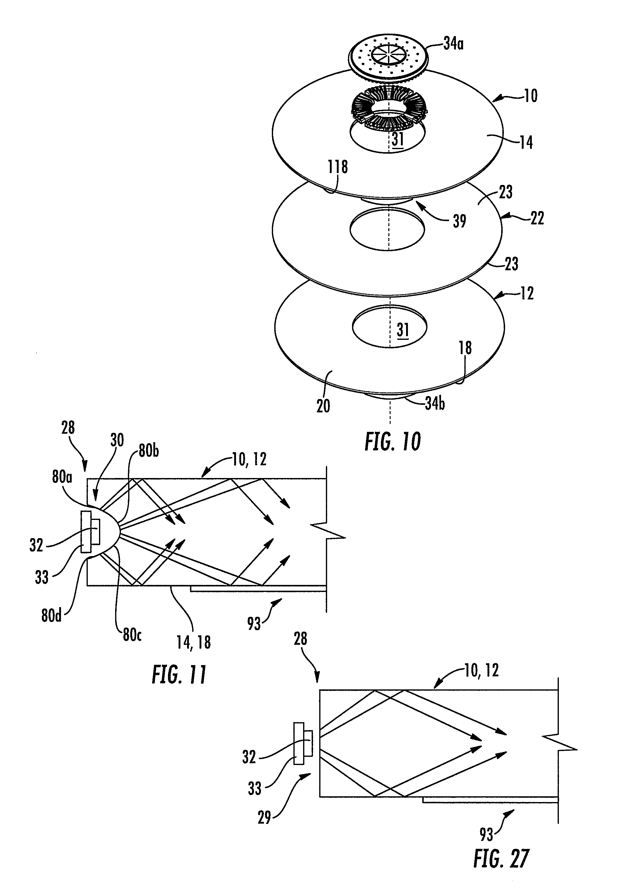
FIG. 10 is an exploded isometric view of an alternate embodiment of the waveguide assembly in the luminaire of FIG. 1;
FIG. 11 is a partial schematic side view of a waveguide;
FIGS. 12-14 are isometric views of alternate embodiments of the waveguide;
FIG. 15 is an isometric view of an embodiment of a the light extraction feature usable in the waveguides;
FIG. 16 is a side view of the light extraction feature of FIG. 15;
FIGS. 17A, 17B and 17C are isometric, side and end views of an alternate light extraction feature usable in the waveguides;
FIGS. 18A and 18B side and end views of another alternate light extraction feature usable in the waveguides; and
FIG. 19 is a top view of another embodiment of a luminaire;
FIG. 20 is a bottom view of the luminaire of FIG. 19;
FIG. 21 is an isometric view of the luminaire of FIG. 19 including a second user control;
FIG. 22 is an exploded isometric view of the luminaire of FIG. 19
FIG. 23 is a partial schematic side view of a waveguide;
FIGS. 24A, 242B, 24C and 25 are example illumination patterns developed by the luminaire of the invention;
FIG. 26 is a block diagram of an embodiment of the control system of the luminaire of the invention;
FIG. 27 is a partial schematic side view of a waveguide.
DETAILED DESCRIPTION
Embodiments of the present invention now will be described more fully hereinafter with reference to the accompanying drawings, in which embodiments of the invention are shown. This invention may, however, be embodied in many different forms and should not be construed as limited to the embodiments set forth herein. Rather, these embodiments are provided so that this disclosure will be thorough and complete, and will fully convey the scope of the invention to those skilled in the art. Like numbers refer to like elements throughout.
It will be understood that, although the terms first, second, etc. may be used herein to describe various elements, these elements should not be limited by these terms. These terms are only used to distinguish one element from another. For example, a first element could be termed a second element, and, similarly, a second element could be termed a first element, without departing from the scope of the present invention. As used herein, the term "and/or" includes any and all combinations of one or more of the associated listed items.
It will be understood that when an element such as a layer, region or substrate is referred to as being "on" or extending "onto" another element, it can be directly on or extend directly onto the other element or intervening elements may also be present. In contrast, when an element is referred to as being "directly on" or extending "directly onto" another element, there are no intervening elements present. It will also be understood that when an element is referred to as being "connected" or "coupled" to another element, it can be directly connected or coupled to the other element or intervening elements may be present. In contrast, when an element is referred to as being "directly connected" or "directly coupled" to another element, there are no intervening elements present.
Relative terms such as "below" or "above" or "upper" or "lower" or "horizontal" or "vertical" or "top" or "bottom" may be used herein to describe a relationship of one element, layer or region to another element, layer or region as illustrated in the figures. It will be understood that these terms are intended to encompass different orientations of the device in addition to the orientation depicted in the figures.
The terminology used herein is for the purpose of describing particular embodiments only and is not intended to be limiting of the invention. As used herein, the singular forms "a", "an" and "the" are intended to include the plural forms as well, unless the context clearly indicates otherwise. It will be further understood that the terms "comprises" "comprising," "includes" and/or "including" when used herein, specify the presence of stated features, integers, steps, operations, elements, and/or components, but do not preclude the presence or addition of one or more other features, integers, steps, operations, elements, components, and/or groups thereof.
Unless otherwise defined, all terms (including technical and scientific terms) used herein have the same meaning as commonly understood by one of ordinary skill in the art to which this invention belongs. It will be further understood that terms used herein should be interpreted as having a meaning that is consistent with their meaning in the context of this specification and the relevant art and will not be interpreted in an idealized or overly formal sense unless expressly so defined herein.
Unless otherwise expressly stated, comparative, quantitative terms such as "less" and "greater", are intended to encompass the concept of equality. As an example, "less" can mean not only "less" in the strictest mathematical sense, but also, "less than or equal to."
The terms "LED" and "LED device" as used herein may refer to any solid-state light emitter. The terms "solid state light emitter" or "solid state emitter" may include a light emitting diode, laser diode, organic light emitting diode, and/or other semiconductor device which includes one or more semiconductor layers, which may include silicon, silicon carbide, gallium nitride and/or other semiconductor materials, a substrate which may include sapphire, silicon, silicon carbide and/or other microelectronic substrates, and one or more contact layers which may include metal and/or other conductive materials. A solid-state lighting device produces light (ultraviolet, visible, or infrared) by exciting electrons across the band gap between a conduction band and a valence band of a semiconductor active (light-emitting) layer, with the electron transition generating light at a wavelength that depends on the band gap. Thus, the color (wavelength) of the light emitted by a solid-state emitter depends on the materials of the active layers thereof. In various embodiments, solid-state light emitters may have peak wavelengths in the visible range and/or be used in combination with lumiphoric materials having peak wavelengths in the visible range. Multiple solid state light emitters and/or multiple lumiphoric materials (i.e., in combination with at least one solid state light emitter) may be used in a single device, such as to produce light perceived as white or near white in character. In certain embodiments, the aggregated output of multiple solid-state light emitters and/or lumiphoric materials may generate warm white light output having a color temperature range of from about 2200K to about 6000K.
Solid state light emitters may be used individually or in combination with one or more lumiphoric materials (e.g., phosphors, scintillators, lumiphoric inks) and/or optical elements to generate light at a peak wavelength, or of at least one desired perceived color (including combinations of colors that may be perceived as white). Inclusion of lumiphoric (also called `luminescent`) materials in lighting devices as described herein may be accomplished by direct coating on solid state light emitter, adding such materials to encapsulants, adding such materials to lenses, by embedding or dispersing such materials within lumiphor support elements, and/or coating such materials on lumiphor support elements. Other materials, such as light scattering elements (e.g., particles) and/or index matching materials, may be associated with a lumiphor, a lumiphor binding medium, or a lumiphor support element that may be spatially segregated from a solid state emitter.
The luminaire as described herein provides a controllable light source that in some embodiments may provide general illumination and may function as a desk lamp, floor lamp or other lamp. The luminaire comprises a light emitting portion comprised of at least two light guides or waveguides (hereinafter "waveguides") emitting light in two different axial directions where the directions may be generally opposite directions (e.g., `upwards` and `downwards`, `left` and `right`, etc.), controllable independently in intensity, emission pattern and/or light properties. As used herein "light properties" of the emitted light refers to properties of the light including, color, color temperature, brightness, CRI (color rendering index), and color gamut (the entire range of colors available on a particular device). The light emitting portion may be predominantly transparent or, in some embodiments, a reflective element may be inserted between the two waveguides to separate the oppositely directed light emissions. The combination of two waveguides allows, for example, for downwards illumination towards a reading or working surface and for upwards illumination towards a ceiling to provide omni-directional illumination.
In some embodiments, radial or lateral control over the light distribution may be provided in addition to the axial control such that the light distribution is controllable in two generally orthogonal planes. In one configuration, for example, a light source provides light into each of the waveguides at an internal edge of the waveguides. The light sources may be divided into groups such as quadrants such that when the luminaire is placed near a wall or in a corner, the light source groups pointing towards the wall or corner may be dimmed (to reduce less useful indirect lighting) in favor of light directed away from the wall to provide more direct illumination (e.g. in `reading` mode). Alternately, light towards the wall or corner may be increased relative to light directed away from the wall to provide more indirect illumination (e.g., TV viewing mode).
The overall illumination pattern can be adjusted to obtain different light distributions to increase overall lighting control and allow for changes in the lighting ambiance. Moreover, the control provided by the two oppositely disposed, independently controlled waveguides provides energy savings.
The emission pattern of the oppositely directed waveguides can be designed to accommodate different situations. The user can set the preferred illumination levels via local controls (e.g. independent capacitive sliders or a single capacitive slider with multitouch capabilities) or remote controls (e.g. Bluetooth via mobile phone). In the case of local control, a 360.degree. multitouch scroll wheel at the base of the luminaire allows access to controls from any direction. The luminaire may also detect stimuli, such as occupancy, in the surrounding environment and automatically dim or turn off the light sources to reduce energy consumption when no stimuli are detected. Furthermore, the luminaire may be equipped with a real time ambient light sensor that allows the luminaire to maintain a constant light level. Further connectivity can be obtained with Wi-fi and integration using Cree SmartCast technology. All components are miniaturized and fit within the housing holding the waveguides.
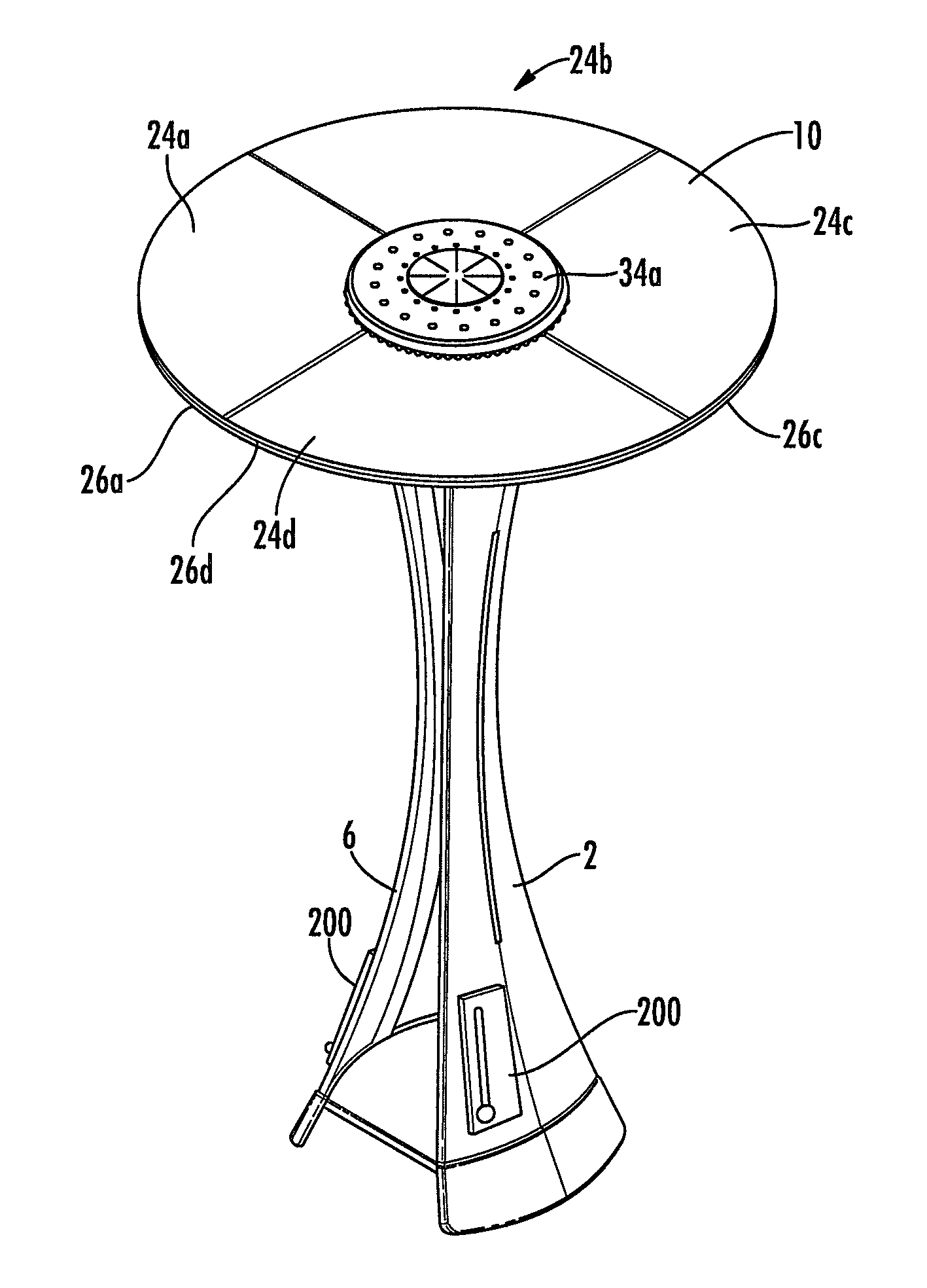
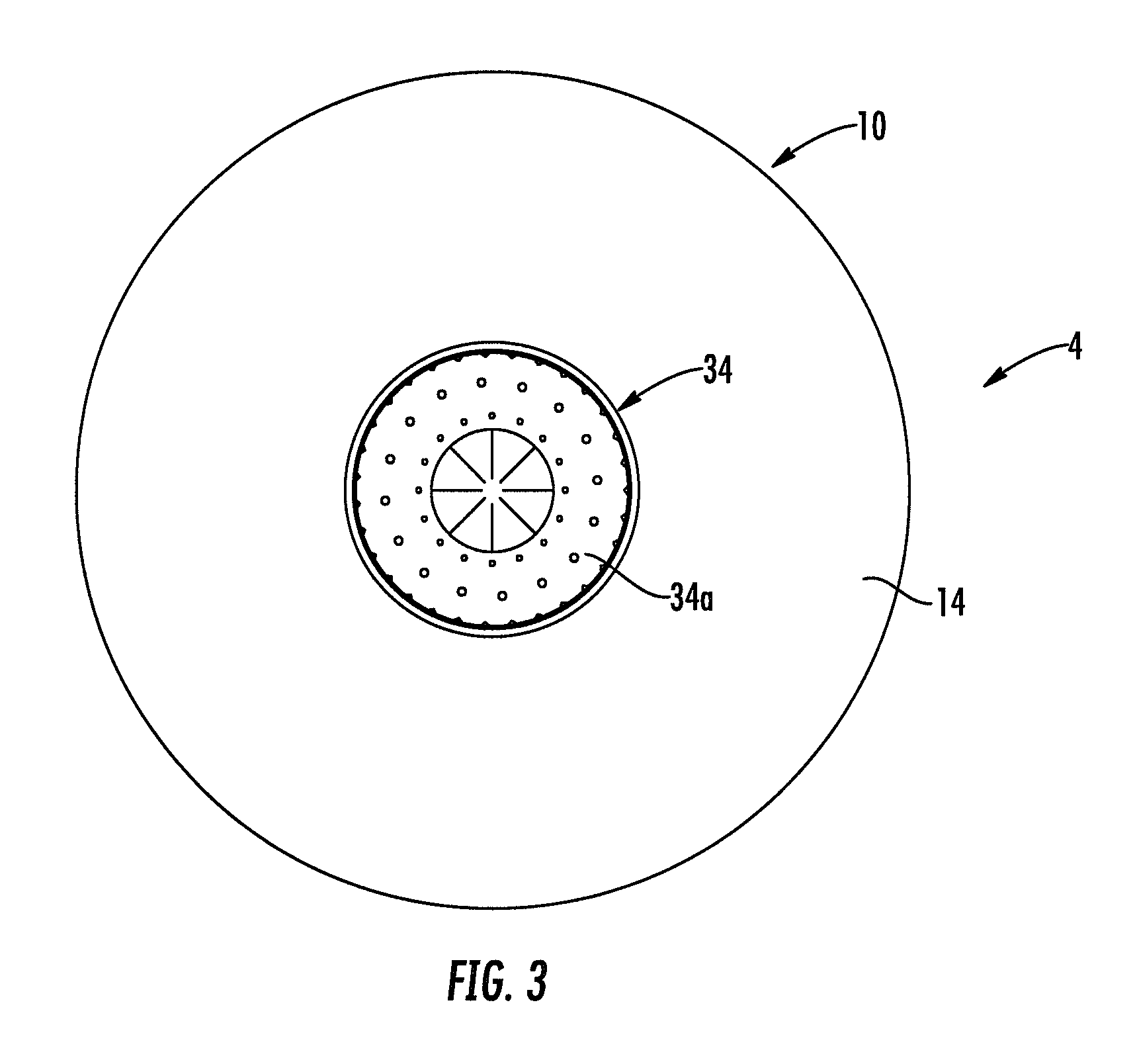
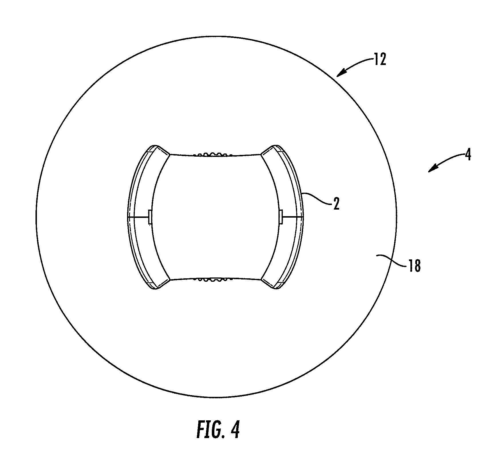
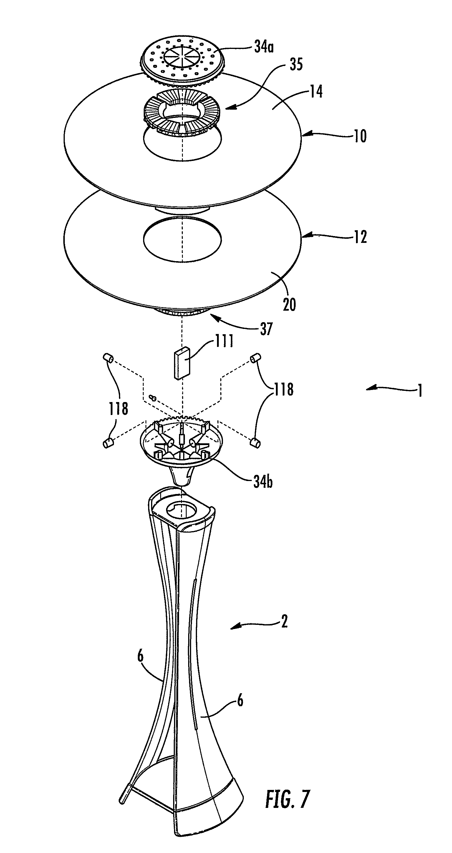
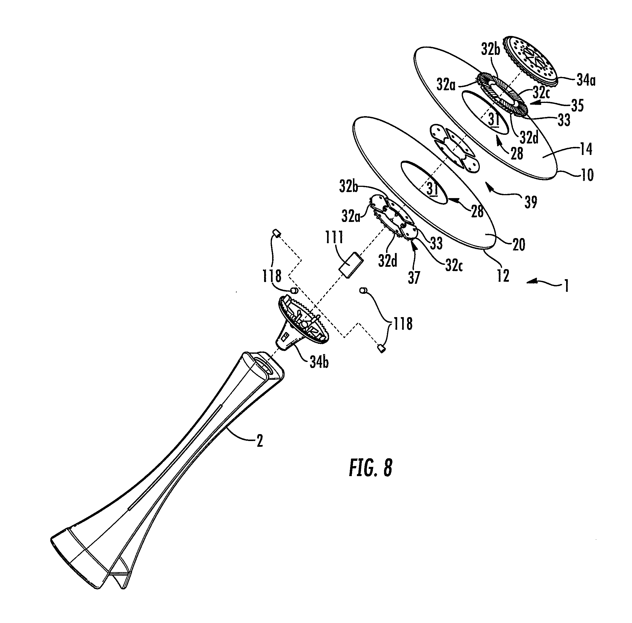
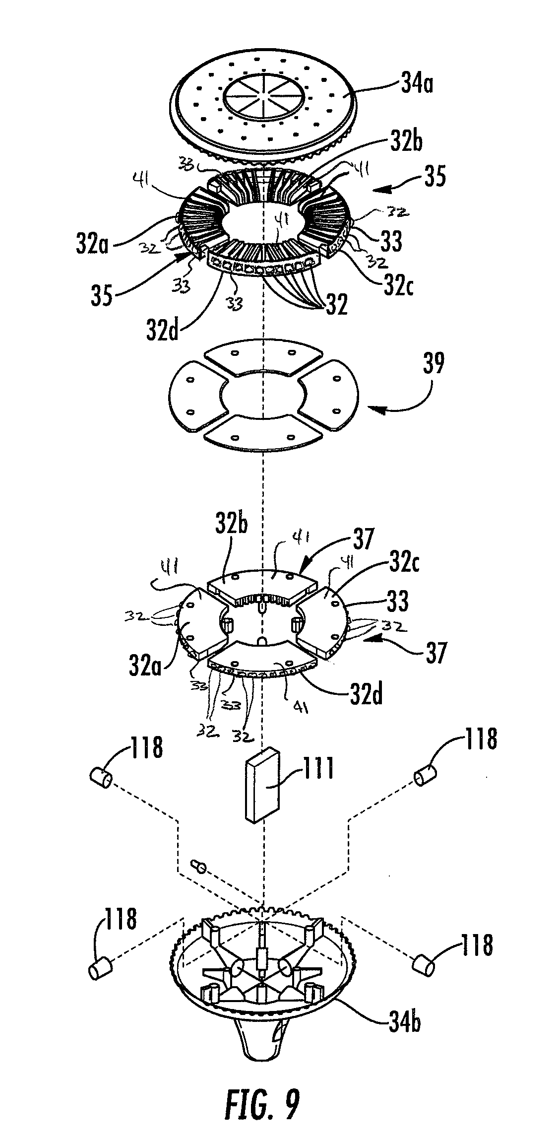
In one embodiment, the luminaire 1, as shown in FIGS. 1 and 2, is configured to provide controllable axial illumination in two directions A and B (e.g. uplight and downlight) along the longitudinal axis A-B of the luminaire. Uplight may be considered to be light directed generally vertically upwards and downlight may be considered to be light directed generally vertically downwards. While the luminaire of FIGS. 1 and 2 is configured to provide controllable axial uplight and downlight, the luminaire may be configured to direct axial light substantially horizontally or at any angle between vertical and horizontal. The luminaire comprises a support structure 2 for supporting the light emitting portion 4 of the luminaire in the desired position and orientation. In the illustrated embodiment the support structure 2 is vertically oriented and comprises a pair of towers 6 that define a horizontal base 6a that may support the luminaire on a floor, desk, table or other horizontal structure such that the light emitting portion 4 is spaced a suitable distance from the supporting horizontal structure. In one embodiment the support structure 2 and light emitting portion 4 are configured as a table lamp such that the luminaire has the general dimensions of a table lamp and may be supported on a table to provide general illumination. The support structure 2 may have virtually any configuration and dimensions and may comprise an ornamental design suitable for interior design and decor considerations other than that shown in the drawings.
While in the illustrated embodiment, the luminaire 1 is configured as a table or floor lamp, the support structure 2 may comprise any suitable supporting elements and may be used as other than a floor, desk or table lamp. For example, the support structure 2 may include a mounting structure such as brackets that may be configured to be secured to a wall or other structure, the support structure 2 may include a clamp to allow the luminaire to be releasably secured to a surface, the support structure 2 may include a cables or rods that allow the luminaire to be suspended from a ceiling, or the support structure 2 may have other suitable configurations.
The light emitting portion 4 of the luminaire comprises at least two waveguides arranged to emit light in two different primary axial directions. In the illustrated embodiment, waveguide 10 emits light in a first axial direction A that is primarily upwards and waveguide 12 emits light in a second axial direction B that is primarily downwards. The first waveguide 10 may comprise a primary light emitting surface 14 directed toward the first axial direction A and a secondary light emitting surface 16 facing the second axial direction B and disposed adjacent to the second waveguide 12. The second waveguide 12 may comprise a primary light emitting surface 18 directed toward the second direction B and a secondary light emitting surface 20 facing the first axial direction A and disposed adjacent to the secondary light emitting surface 16 of the first waveguide. In this manner the first waveguide 10 emits light primarily in the first axial direction A (upwardly) and the second waveguide 12 emits light primarily in the second axial direction B (downwardly). The waveguides 10, 12 may be constructed of a substantially transparent or translucent material such that the light emitting portion 4 is substantially transparent or translucent. In this configuration some light may exit the secondary light emitting surfaces 16, 20 of the waveguides 10, 12 such that the first waveguide 10 emits a small portion of light as downlight and the second waveguide 12 emits a small portion of light as uplight. Further, the illumination distribution may be visible through the waveguides along a line of sight extending along axis A-B. The optical waveguides 10, 12 exhibit a luminance from the secondary light emitting surfaces 16, 20 along the line of sight that is less than about 20%, preferably less than about 10%, and most preferably less than about 5% of the total luminance of the luminaire such that in some embodiments the primary light emitting surfaces emit at least 80% to at least 95% of the total luminance of the luminaire and in a preferred embodiment emit greater than about 95% of the total luminance of the luminaire.
In other embodiments a backplane 22 may be disposed between the waveguides 10, 12 such that the first waveguide 10 generates only light in direction A and the second waveguide 12 generates only light in direction B as shown in FIG. 10. The backplane 22 may comprise a part of the support structure 2 or may be separate therefrom. The backplane 22 may include surfaces 23 adjacent the secondary light emitting surfaces 16, 20 that has a white or specular reflective coating or other member secured or otherwise applied thereto. Light exiting the surfaces 16, 20 of the waveguides 10, 12 is reflected off the surfaces 23 and re-directed through the same waveguide so that the light contributes to the luminous intensity distribution of the light emitted from the primary light emitting surface of that waveguide. Each waveguide 10, 12 may comprise a separate backplane member or a single backplane member may be disposed between the waveguides. In some embodiments, a reflective or diffusive edge baffle may encircle the exterior edges of waveguides 10, 12 to prevent the appearance of a bright line pattern on an adjacent wall and to maximize waveguide extractor uniformity.
As shown in FIGS. 8, 11 and 27 each waveguide 10, 12 includes an input portion 28 having a light coupling feature for delivering the light emitted from the LEDs to the waveguide. The light coupling feature may comprise additional lenses, optics or the like. One or more LED elements or modules (hereinafter "LEDs") 32 are disposed in or adjacent the input portion 28 of each of the waveguides 10, 12 and direct the emitted light into the coupling feature 30. In one embodiment the light coupling feature is in the form of a cavity 30 for receiving light from the LEDs 32 and delivering the light to the waveguides 10, 12. The annular cavity 30 may be disposed at the inner edge of each of the waveguides 10, 12 such that the waveguides are edge-lit from the inner edge thereof. Where the light coupling feature 30 is a cavity, the cavity may be defined by a plurality of surfaces 80a, 80b, 80c, 80d. The surfaces 80 are designed to cause light developed by the one or more LEDs 32 disposed in or adjacent the light coupling feature 30 to be redirected into at least two groups or sets of light rays each of which travels within a range of ray angles through each waveguide or waveguide section. According to well-known TIR principles, the light rays of the groups continue to travel through the waveguides, respectively, until such rays strike an index interface surface at a particular angle less than an angle measured with respect to a line normal to the surface point at which the light ray is incident or, equivalently, until the light rays exceed an angle measured with respect to a line tangent to the surface point at which the light ray is incident, and the light rays escape. Other types of couplings and/or orientation of the LEDs 32 relative to the waveguides 10, 12 may be used. For example as shown in FIG. 27 the coupling feature at the input portion 28 of the waveguide may be a planar surface 29 that is disposed substantially perpendicularly to the LEDs 32. The coupling feature 29, 30 at the inner edges of the waveguides 10, 12 may be formed by apertures 31 formed substantially in the center of the waveguides although the aperture may be positioned off-center in the waveguides if desired. The type of coupling may influence the angular and spatial distribution of light within the waveguide, which in turn can influence the efficiency of extraction, the illuminance, and the luminance
Each LED 32 may be a single white or other color LED chip or other bare component, or each may comprise multiple LEDs either mounted separately or together on a single substrate or package to form a module including, for example, at least one phosphor-coated LED either alone or in combination with at least one color LED, such as a green LED, a yellow LED, a red LED, etc. In those cases where a soft white illumination with improved color rendering is to be produced, each LED 32 may include one or more blue shifted yellow LEDs and one or more red LEDs. The LEDs may be disposed in different configurations and/or layouts as desired. Different color temperatures and appearances could be produced using other LED combinations, as is known in the art. In one embodiment, the LED 32 comprises, for example, an MT-G LED incorporating TrueWhite.RTM. LED technology developed and manufactured by Cree, Inc., the assignee of the present application, or as disclosed in U.S. patent application Ser. No. 13/649,067, filed Oct. 10, 2012, entitled "LED Package with Multiple Element Light Source and Encapsulant Having Planar Surfaces" by Lowes et al., the disclosure of which is hereby incorporated by reference herein in its entirety. If desirable, a side emitting LED may be utilized inside the waveguide body such as disclosed in U.S. Pat. No. 8,541,795, the disclosure of which is incorporated by reference herein in its entirety. Various types of LEDs may be used, including LED packages having primary optics as well as bare LED chips. The luminaire may include LEDs 32 of the same type of phosphor-converted white LED, or any combination of the same or different types of LEDs discussed herein. In some embodiments, a luminaire may include a plurality of groups of LEDs 32, where each group may include LEDs 32 having different colors and/or color temperatures. The groups of LEDs 32 may be separated by dividers, as described in U.S. patent application Ser. No. 14/472,035, filed Aug. 28, 2014, entitled "Luminaire Utilizing Multiple Edge Coupling" by Tarsa et al., which is incorporated by reference herein in its entirety, wherein the LEDs 32 are disposed within the coupling cavity. Such dividers facilitate the mixing of light between adjacent LEDs 32, limit the angle of incidence of light incident on the coupling surfaces of the waveguide, and reduce interaction and light absorption between LED components. In embodiments having LEDs of the same or similar color, dividers may not be necessary or desired. In any of the embodiments disclosed herein the LED element(s) or module(s) 32 may have a Lambertian or near-Lambertian light distribution, although each may have a directional emission distribution (e.g., a side emitting distribution), as necessary or desirable. More generally, any Lambertian, near-Lambertian, symmetric, wide angle, preferential-sided, or asymmetric beam pattern LED(s) may be used as the light source. The color, color temperature, brightness, CRI, and color gamut of the emitted light are referred to herein as the light properties of the emitted light and may be controlled by the user in addition to controlling the light emission pattern.
The LEDs may form part of LED assemblies 35 and 37 disposed adjacent the input portion 28 of the waveguides 10, 12, respectively. The LED assemblies 35, 37 may comprise an LED board 33 such as a PCB or a flexible PCB, such as a flex circuit, that supports a plurality of LEDs 32 arranged in a circular or cylindrical configuration such that light from the LEDs is directed into the light coupling feature 29, 30 of the waveguides 10, 12. The LED board 33 may physically support the LEDs and form part of the electrical path from the lamp electronics to the LEDs. The LED boards 33 may be mounted on heat sink structures 41 that may comprise heat dissipating elements such as fins for dissipating heat from the LEDs 32. The LEDs are arranged such that the LEDs of the first LED assembly 35 direct light into waveguide 10 and the LEDs of the second LED assembly 37 direct light into waveguide 12. The LEDs of the two LED assemblies 35, 37 are independently controllable such that the waveguides 10 and 12 may be independently illuminated. The LEDs of the two LED assemblies 35, 37 may be mounted on separate LED boards, as shown, or the two sets of LEDs may be mounted on a single LED board provided that the two sets of LEDs are independently controllable to illuminate the waveguides 10 and 12 independently of one another. As shown, the LED assemblies 35, 37 are disposed at the inner peripheral edges of the waveguides 10 and 12 such that light from the LEDs 32 is optically coupled to the waveguides at the inner edges thereof. Spacers 39 may be provided to isolate the LED assemblies 35, 37 from one another.
While the LED assemblies 35, 37 with LEDs 32 may be disposed at an input portion 28 of the waveguides 10, 12 that is positioned at an inner edge of the waveguides such that the LEDs direct light primarily outwardly as described above, the LED assemblies 35, 37 may be disposed at an input portion 28 of the waveguides that is positioned at an outside peripheral edge of the waveguide such that the LEDs direct light primarily inwardly as shown in FIG. 12. In such an embodiment apertures 31 may be eliminated. In the embodiments of FIGS. 1-12, the waveguides 10, 12 are generally circular in shape. However, in other embodiments the waveguides may have other shapes including, but not limited to, oval, rectangular (see FIGS. 13 and 14), polygonal or the like. Moreover, in some embodiments the shape of waveguide 10 may different that the shape of waveguide 12. In some embodiments the LED assemblies 35, 37 may be disposed along less than the entire peripheral edge of the waveguide. For example, as shown in FIG. 14 the LED assembly 35 associated with the waveguide 210 is disposed at two outer edges of the rectangular waveguide 210.
Referring to FIG. 1, the waveguides 10, 12 extend from a housing or enclosure 34 having a first part 34a and a second part 34b. The first and second parts 34a, 34b may be held together by fasteners (not shown), although any suitable fastening means may be used to trap the waveguides 10, 12 therebetween to support the waveguides relative to the support structure 2. The housing 34 also supports the LED assemblies 35, 37 and at least some of the control electronics for the luminaire. The support structure 2 may be physically connected to the enclosure 34 to support the waveguides in the desired position and orientation.
Referring to FIGS. 11, 27 and 15-18B, extraction features are disposed on the light emitting sides 14, 18 of the waveguides 10, 12. In some embodiments, the extraction features 93 are not visible to the viewers in the room. In other embodiments, the extraction features are arranged in a regular array such as a hexagonal close-packed array. In still other embodiments, the extraction features are arranged in a specific pattern (density pattern) in order to improve optical efficiency, luminance uniformity, or provide a desired visual effect. One or more extraction features 93 disposed on the primary light emitting surfaces 14, 18 cause the light to exit the waveguides 10, 12 in a controlled fashion such that light is directed out of the first and second primary light emitting surfaces. Because the light rays are at least substantially collimated they experience minimal spreading as they propagate through the waveguides. This results in highly controlled beams that can be either extracted in a collimated fashion, or spread into a wide distribution.
As shown in FIG. 15 the plurality of light extraction features 93 comprises an array 110 of regularly-spaced features 112, although it should be noted that the light extraction features may be irregularly spaced or some may be regularly spaced and others irregularly spaced, etc. In the illustrated embodiment, the light extraction features 93 are disposed in a hexagonal array and are disposed on a substrate 114, which may be a planar member, such as a film, a plate, a block or material, or the like. Further in the illustrated embodiment, the light extraction features 93 comprise protrusions carried by a film where the protrusions are disposed between the film and the primary light emitting surfaces 14, 18.
The substrate 114 having features 93 disposed thereon may be fabricated using one of a variety of techniques typically applied to the formation of micro-optical films, including gray-scale lithography, micro-replication, injection/compression molding, reactive ion etching, chemical embossing, or drum roll transfer. Other methods of fabrication include dispensing an acrylic-based UV resin or silicone material on a carrier film that is subsequently cured to form extraction features.
In some embodiments, the extraction features 93 may be disposed on the waveguides 10, 12 without a substrate 114. For example, the extraction features 93 may be fabricated directly on the surfaces 14, 18 of the waveguides 10, 12 by means of an intermediate patterning layer as described in U.S. Pat. No. 8,564,004, issued Oct. 22, 2013, entitled "Complex Primary Optics with Intermediate Elements" by Tarsa et al., incorporated by reference herein in its entirety. Using this method of manufacture, the extraction features 93 are optically joined to the waveguides 10, 12 without the need for the substrate 114. The patterning layer may be used with any method such as molding, injection molding, compression molding, dispensing, stencil printing, three-dimensional printing, photolithography, deposition, or the like. Specifically, the patterning layer is formed on the primary light emitting surfaces 14, 18 of the waveguides 10, 12 and includes holes or openings where the surface of the waveguide is exposed. The openings of the patterning layer correspond to locations where the extraction features are to be formed on the waveguide. In some embodiments, a mold is then placed over the patterning layer and the surfaces 14, 18 of the waveguides 10, 12. The mold includes voids that are aligned with the openings of the patterning layer to define cavities. The cavities are filled with the material of the extraction features to form the extraction features on the waveguides. In other embodiments, the material of the extraction features is applied to the openings of the patterning layer prior to placement of the mold on the patterning layer. In either case, the material of the extraction feature is then at least partially cured and the mold is removed. The material of the patterning layer may comprise polyvinyl alcohol, a poly(methyl methacrylate) (PMMA) one or more photoresist materials, or other suitable materials. The patterning layer may be removed by a water rinse, heat, vaporization, machining, developers and solvents, chemical etching/solvent, plasma etching, or any method that does not interfere with the material of the waveguides and/or extraction features. Alternatively, the waveguides 10, 12, the extraction features 93, and/or the substrate 114 may be bonded to one another through one or more supplemental layers such as an adhesive layer or pressure-sensitive adhesive film.
The light extraction features 93 may be of the same material as the substrate 114 and/or the waveguides 10, 12, or the materials of the features 93, the substrate 114, and/or the waveguides 10, 12 may be different. In any event, the material(s) of the features 93 and the substrate 114, as well as the waveguides 42, preferably comprise optical grade materials that exhibit TIR characteristics including, but not limited to, one or more of acrylic, air, polycarbonate, molded silicone, glass, and/or cyclic olefin copolymers, and combinations thereof, possibly in a layered arrangement, to achieve a desired effect and/or appearance. Preferably, although not necessarily, the features 93 are all solid or some or all have one or more voids or discrete bodies of differing materials therein. In some embodiments, the features 93 are preferably (although not necessarily) of substantially the same size (except, perhaps height extending from the substrate 114) and preferably (but not necessarily) have substantially the same shape, with minor variations in the shape utilized to produced specific luminous intensity patterns. In other embodiments, the size and shape of extractors vary significantly between waveguides or regions of waveguides to produce differing luminous intensity patterns. In still other embodiments, the symmetry or material of the extractors may vary in order to produce differing luminous intensity patterns.
The illuminance distributions of the waveguides 10, 12 are dependent upon the particular geometry and arrangement of extraction features 93. The features 93 may preferably have a truncated hemispherical shape as shown in FIGS. 15 and 16, although other shapes are possible. Another geometry which is particularly useful for a range of lighting applications, includes a roughly "bullet shaped" profile as illustrated in FIGS. 17A-17C, consisting of a truncated curved surface 94 such as a truncated hemisphere with an adjacent cylindrical or conical base 96. This particular geometry provides a high degree of directionality as well as a range of possible illuminance distributions that may be realized by changing the height at which the curved surface is truncated. The high directionality (i.e., ratio of `downward` emitted light to `upward` emitted light) can help minimize efficiency loss by minimizing reflections off of a backplane reflective member 22 or eliminate the need for the reflective backplane member altogether, thereby reducing system cost. The height A of the hemispherical portion 94 affects the distribution of the light illumination of each waveguide 10, 12 while the height C of the base 96 affects predominantly the percentage of light emitted downwardly relative to upward emitted light. If desired, a bonding feature 98 having a central planar portion 99 may be formed atop the truncated hemispherical portion 94. In some embodiments, the bonding feature 98 facilitates fabrication by enabling the bond between the feature 93 and the waveguide surfaces to be free of air pocket(s) that may otherwise form. In general, the bonding feature 98 of each extraction feature is bonded, laminated, or otherwise optically coupled to the primary light emitting surfaces such that the bonding feature 98 is embedded in the interposing adhering layer and results in a planar bond between the extraction feature 93 and the waveguide surfaces.
Further example extraction features 116 are illustrated in FIGS. 18A and 18B. Each extraction feature 116 includes a body 119 having a curved shape that extends between an aperture 120 adjacent the surfaces of the waveguides 10, 12 and a base 122 opposite the bonding feature 134. The body 118 may include planar surfaces, curved surfaces, planar surfaces approximating a curve, or a combination thereof. The cross sectional outer profile of the body 118 may be symmetric in nature (e.g., as in the case of a hemisphere) or asymmetric (e.g., as in the case of an ellipse or other combination of shapes). The extraction features 116 and/or waveguides 10, 12 may be acrylic, including an acrylic UV-curable resin, silicone, polycarbonate, glass, or other suitable material(s) and combinations thereof, possibly in a layered arrangement, to achieve a desired effect. The body 118 may include a first portion 124 adjacent the bonding feature 134 and a second conical portion 126 adjacent the base 122. In some embodiments, the first portion 124 may be designed to redirect incident light downward through total internal reflection (TIR). In still further embodiments, the extraction features 116 may have an asymmetric shape. For example, the first portion 124 of the extraction feature 116 may be hemispherical and the base 122 may be elliptical such that the feature 116 appears as a truncated hemisphere when viewed from any cross-section, but appears as an ellipse or elongated circle when viewed from the top or bottom. Such asymmetric geometry would result in an asymmetric illuminance pattern such that may be desired for certain applications. Further, the extraction features 93, 116 having an asymmetric cross-section along the height H may direct light into particular directions or quadrants below the luminaire. Extraction features 93, 116 with segmented cross-sections and top or bottom profiles consisting of a combination of curved surfaces and linear surfaces (such as an extractor that appears as a truncated hemisphere from the side, but appears as a star-shape or faceted shape from above) may be used for specific lighting applications requiring a very unique and defined illuminance distribution (e.g., stage lighting, architectural or cove lighting). Still further, extraction features having a generally conic shape (symmetric or asymmetric, truncated or not) may produce more collimated light beams in specific directions (e.g., for direct/indirect pendant lighting, downlighting, etc.). The shape of the extraction features may be determined as set forth in U.S. patent application Ser. No. 14/472,064, filed Aug. 28, 2014, entitled "Luminaire with Selectable Luminous Intensity Pattern" by van de Ven et al., which is incorporated by reference herein in its entirety.
Referring to FIG. 9, for example, the LEDs 32 may be arranged to divide the light emitting portion 4 into sections such that the light emission pattern of the lamp may be controlled laterally as well as axially. The LEDs 32 in each of LED assemblies 35 and 37 are arranged in a plurality of LED groups 32a, 32b, 32c, 32d where the light emitted by the LEDs in each of the LED groups may be controlled independently of the LEDs in the other LED groups. In the illustrated embodiments the LED board 33 and heat sinks 41 are divided into separate elements, one associated with each of the LED groups; however, a single LED board and a single heat sink structure may be used provided the LED groups are independently controllable. By selectively controlling the light emitted by the LEDs in each LED group 32a, 32b, 32c, 32d of LED assemblies 35 and 37 the lateral distribution of the light may be controlled. For example if all of the LED groups 32a, 32b, 32c, 32d are illuminated the luminaire emits light omni-directionally such that the light is emitted in 360 degrees about the axis of the lamp. If two adjacent LED groups 32a, 32b of the luminaire are illuminated the luminaire emits light directionally where light is emitted primarily to the side of the luminaire on which the LED groups are illuminated and substantially less light is emitted to the side of the luminaire where the non-illuminated LED groups are directed. The LED groups may also be illuminated in other patterns such as illuminating fewer than half of the LED groups, illuminating more than half of the LED groups, alternating illuminated LED groups with non-illuminated LED groups or the like to create different light emission patterns and effects. Moreover, while four LED groups 32a, 32b, 32c, 32d are shown a greater or fewer number of LED groups may be provided. The more LED groups that are provided, the more fine the control over the light pattern. Also, the LED groups may be illuminated at different power levels and/or with different light properties to further vary the light emission pattern.
The multiple LED groups 32a, 32b, 32c, 32d may be used with monolithic waveguides 10, 12, shown in FIGS. 1-14 where the pattern of the light emitted by each waveguide is controlled by selective activation of the LED groups 32a, 32b, 32c, 32d associated with that waveguide. It will be appreciated that in such an embodiment as the light fans out from the LEDs 32 some of the light may be transmitted across and be emitted from the waveguide at locations laterally spaced from the activated LEDs. The emitted light will be brightest in the portions of the waveguide into which the activated LEDs are directed and the emitted light will diminish in intensity in areas of the waveguide that are optically spaced from the activated LED groups. Thus, referring to FIG. 8, if the two LED groups 32a, 32b are illuminated and two LED groups 32c, 32d are not illuminated the majority of the light will be emitted from the waveguides in the area of the waveguides 10, 12 that directly receive the light emitted from the illuminated LED groups 32a, 32b (the area to the left of the broken line in FIG. 8) while less of the light will be emitted from areas of the waveguides optically spaced from the illuminated LED groups (the area to the right of the broken line in FIG. 8). The intensity of the emitted light will gradually diminish across the waveguides from the directly illuminated areas of the waveguides to the non-directly illuminated areas of the waveguides. Thus, while a laterally directional light emission pattern is developed where half of the waveguides are directly illuminated, at least some light may be transmitted through the remainder of the waveguides and be emitted from the non-directly illuminated areas such that the transition between the directly illuminated part of the waveguides and the non-directly illuminated part of the waveguides will be gradual.
In some embodiments, in addition to arranging the LEDs as independently controllable LED groups, each of the waveguides 10, 12 may be divided into sections that provide further additional control over the light emission pattern. As shown in FIGS. 19-22 the first waveguide 10 may comprise multiple waveguide sections 24a, 24b, 24c and 24d that are arranged in a side-by-side substantially coplanar array where each waveguide section is disposed adjacent at least one other waveguide section. Likewise, the second waveguide 12 may comprise multiple waveguide sections 26a, 26b, 26c and 26d that are arranged in a side-by-side substantially coplanar array wherein each waveguide section is disposed adjacent at least one other waveguide section. If desired, optional optical isolation members in the form of reflective barriers 28 may be disposed between some or all of the adjacent waveguide sections. Each reflective barrier 28 may comprise a specular or white reflective member or film that extends partially or completely between adjacent waveguide sections 24a-24d, 26a-26d so that the adjacent waveguides are partially or fully optically isolated, respectively, with respect to one another. In some embodiments the separate waveguide sections may be formed by physically separate parts as shown in FIGS. 19-22. In other embodiments, a single part may form the waveguide where the waveguide sections are optically separated from one another such as by providing optical barriers between the sections as shown in FIG. 23. The optical barriers may be gaps 27 formed between the primary light emitting surfaces of the waveguide sections as shown in FIG. 23. In other embodiments, the optical barriers may comprise reflective barriers 28 that may be, for example, insert molded between the waveguide sections during manufacture of the waveguides. Other mechanisms for optically separating the waveguide sections may be used.
In the illustrated embodiment, the waveguides 10, 12 are generally circular in shape. In such an embodiment, if waveguide sections are provided each waveguide section may be formed essentially as a sector of a circle as shown in FIGS. 19-22. However, in other embodiments the waveguides may have other shapes including, but not limited to, oval, rectangular (see FIGS. 13 and 14), polygonal or the like and the waveguide sections may have shapes other than the sector shaped sections selected to create the waveguide and to generate a desired light emission profile, an example of such sections 210a-210d are shown in FIG. 14. Moreover, while in the illustrated embodiments each waveguide 10, 12 is shown made up of four waveguide sections a fewer or greater number of waveguide sections may be used to create each waveguide. Each waveguide 10, 12 and waveguide section may have any suitable shape, and the shapes of the waveguides and waveguide sections may be different from one another or substantially identical. Moreover, the light emitting elements formed on each of the primary light emitting surfaces of the waveguide sections may be different, as previously described, such that each waveguide section may have a different light emission pattern than other ones of the waveguide sections of the same waveguide.
As shown in FIG. 22 each of the waveguides 10, 12 may comprise a plurality of optically decoupled waveguide sections 24a, 24b, 24c, 24d and 26a, 26b, 26c, 26d, respectively. One of each of the waveguide sections of waveguide 10 may be optically coupled to one of LED groups 32a-32d of LED assembly 35 such that the light emitted by each one of the LED groups is emitted from the waveguide 10 only via the waveguide section optically coupled to that LED group. Likewise, one of each of the waveguide sections of waveguide 12 may be optically coupled to one of LED groups 32a-32d of LED assembly 37 such that the light emitted by each one of the LED groups is emitted from the waveguide 12 only via the waveguide section optically coupled to that LED group. The waveguide sections may be in a one-to-one relationship with the LED groups or each waveguide section may be optically coupled to more than one LED group. As previously described, each waveguide 10, 12 may comprise multiple waveguide sections that are maintained in a side-by-side array wherein each waveguide section is disposed adjacent at least one other waveguide section. The light emitted by each LED group is transmitted to the waveguide section that is optically coupled to that LED group such that light generated by that LED group is substantially only emitted from the associated waveguide section. Such an arrangement may be used to provide sharper delineation between the light emitted from one waveguide section of the waveguide and the light emitted from a different waveguide section of the waveguide as compared to the more gradual transition described above with respect to FIGS. 1-11.
Moreover, different waveguide sections of the waveguides 10, 12 may be provided with different light extracting properties such that light emitted from one section of the wave guide has a different emission pattern than light emitted from another section of the waveguide. Where the waveguide is divided into sections each section may be easily provided with different light extracting properties. However, each section of the waveguide may be provided with different light extraction properties even where a single waveguide is used as shown in FIG. 23. Because each of the LEDs associated with each of the waveguide sections is independently controllable and dimmable the luminaire may produce a variety of light emission patterns.
In the illustrated embodiment the primary light emitting surfaces 14, 18 of the waveguides 10, 12 are disposed horizontally to emit light primarily upwardly and downwardly respectively. The axis A-B along which the primary light emitting surfaces emit light may be considered the axial orientation of the luminaire where as illustrated the axial orientation is vertical. It will be appreciated that a luminaire may be configured where the axial orientation is horizontal or at any angular location between vertical and horizontal. Moreover, in some luminaires the axial orientation of the waveguides may be adjustable relative to the support structure 2 such that the axial orientation may be changed during use of the luminaire. For example, the light emitting portion 4 of the luminaire may be rotatably or tiltably mounted on support structure 2. The light intensity extends in both directions along the axial orientation and may be independently adjusted in both directions. It is to be understood that the light emitted from the waveguides may be emitted in a variety of light emission patterns such that light is not directed solely along the axis but may be emitted directionally, in a Lambertian pattern or in any other desired pattern where a portion of the light may be emitted in directions at angles to the axis of orientation. FIG. 24A shows an illumination pattern for a luminaire as shown in FIG. 1 where 77% of the emitted light is emitted as downlight D and 23% of the emitted light is emitted as uplight U where the emission is laterally symmetrical; FIG. 24B shows an illumination pattern for a luminaire as shown in FIG. 1 where 78% of the emitted light is emitted as downlight D and 22% of the emitted light is emitted as uplight U where the emission is laterally symmetrical; FIG. 24C shows an illumination pattern for a luminaire as shown in FIG. 1 where 83% of the emitted light is emitted as downlight D and 17% of the emitted light is emitted as uplight U where the emission is laterally symmetrical. While the percentage of emitted uplight and downlight is similar for the three examples, the difference in illumination patterns is caused by the type of light emitting elements formed on the waveguides. In the embodiment of FIG. 24A the light emitting elements are truncated hemispheres, in the embodiment of FIG. 24B the light emitting elements are conical; and in the embodiment of FIG. 24C the light emitting elements are torroidal. The actual illumination patterns may be different than those illustrated and the specific shape and intensity of the illumination patterns may vary widely from those shown. Moreover, the amount of light emitted by each of waveguides 10 and 12 may be increased and/or decreased such that the uplight may be greater than the downlight, the downlight may be greater than the uplight or the light emitted as uplight and downlight may be substantially equal. Additionally, the illumination patterns for the uplight and the downlight may be different from one another. Thus, by selectively and controllably illuminating the waveguides 10, 12 the illumination pattern may be varied along the orientation axis A-B.
FIG. 25 shows an illumination pattern for a luminaire as shown in FIG. 1 where 79% of the light is emitted as downlight and where the light is emitted in a laterally asymmetric pattern such that more light U.sub.1, D.sub.1 is emitted to one side of the luminaire (left as viewed in FIG. 25) and relatively less light U.sub.2, D.sub.2 is emitted to the opposite side of the luminaire (right as viewed in FIG. 25). In the embodiment of FIG. 25, for example, two adjacent waveguide sections of each of waveguides 10 and 12 are illuminated more and the other two adjacent waveguide sections are illuminated less. This type of illumination pattern may be useful if the luminaire is positioned adjacent a wall or in other situations where laterally directional lighting is desired.
The architecture of the luminaire may comprise a core 111 comprising the controller, LED drivers, ambient light sensors and Bluetooth LE. The core may also comprise a power supply such as a 24V AC/DC power supply with 5V regulator. The drivers control operation of the LEDs. The core may be sized and configured to be positioned at the center of the waveguide structure. The core communicates with the PIR sensors and manual sensor described above to control the operation of the LEDs. Referring to FIG. 26, the control architecture for the luminaire includes drivers 110 for operating the LED groups 32a-32d of each of LED assemblies 35 and 37. The drivers 110 may comprise buck converters controlled by two 16 bit PWM for controlling dimming of the LEDs. The luminaire electronics may further comprise a power supply 114 comprising a buck regulator. A controller 116, that in some embodiments comprises a microprocessor, controls the power supply 114 and drivers 110 in accordance with control signals received from passive infrared (PIR) sensors 118, manual control device inputs 122 and/or wireless signals received from wireless interface 120 such as based on Bluetooth technology. Controlling the LEDs allows the LED groups 32a-32d associated with each of the waveguides 10 and 12 and/or waveguide sections 24a-24d and 26a-26d to be independently controlled to control the emission pattern of the light as uplight, downlight and lateral light. Any of the embodiments disclosed herein may include a power circuit having a buck regulator, a boost regulator, a buck-boost regulator, a SEPIC power supply, or the like, and may comprise a driver circuit as disclosed in U.S. patent application Ser. No. 14/291,829, filed May 30, 2014, entitled "High Efficiency Driver Circuit with Fast Response" by Hu et al. which is incorporated by reference herein in its entirety or U.S. Pat. No. 9,303,823, issued Apr. 5, 2015, entitled "SEPIC Driver Circuit with Low Input Current Ripple" by Hu et al. which is incorporated by reference herein in its entirety. The circuit may further be used with light control circuitry that controls color temperature of any of the embodiments disclosed herein in accordance with user input such as disclosed in U.S. patent application Ser. No. 14/292,286, filed May 30, 2014, entitled "Lighting Fixture Providing Variable CCT" by Pope et al. which is incorporated by reference herein in its entirety.
Further, any of the embodiments disclosed herein may include one or more communication components forming a part of the light control circuitry, where the wireless interface 120 may comprise an RF antenna that senses RF energy. The communication components may be included, for example, to allow the luminaire to communicate with other luminaires and/or with an external wireless controller, such as disclosed in U.S. Pat. No. 8,975,827, issued Mar. 10, 2015, entitled "Lighting Fixture for Distributed Control" which is incorporated by reference herein in its entirety or U.S. patent application Ser. No. 14/498,119, filed Sep. 26, 2014, entitled "Handheld Device that is Capable of Interacting with a Lighting Fixture", U.S. patent application Ser. No. 14/498,147, filed Sep. 26, 2014, entitled "Enhanced Lighting Fixture", U.S. patent application Ser. No. 14/498,168, filed Sep. 26, 2014, entitled "Handheld Device for Grouping a Plurality of Lighting Fixtures", U.S. patent application Ser. No. 14/498,197, filed Sep. 26, 2014, entitled "Handheld Device for Merging Groups of Lighting Fixtures", U.S. patent application Ser. No. 14/498,219, filed Sep. 26, 2014, entitled "Handheld Device for Controlling Settings of a Lighting Fixture", U.S. patent application Ser. No. 14/588,762, filed Jan. 2, 2015, entitled "Power Over Ethernet Lighting Fixture", U.S. patent application Ser. No. 14/725,687, filed May 29, 2015, entitled "Power Over Ethernet Lighting Fixture", all of which are incorporated by reference herein in their entirety. More generally, the control circuitry includes at least one of a network component, an RF component, a control component, and a sensor. The sensor may provide an indication of ambient lighting levels thereto and/or occupancy within the room or illuminated area. Such sensor may be integrated into the light control circuitry. In various embodiments described herein various smart technologies may be incorporated in the luminaires as described in the following applications "Solid State Lighting Switches and Fixtures Providing Selectively Linked Dimming and Color Control and Methods of Operating," U.S. Pat. No. 8,736,186, issued May 27, 2014, which is incorporated by reference herein in its entirety; "Master/Slave Arrangement for Lighting Fixture Modules," application Ser. No. 13/782,096, filed Mar. 1, 2013, which is incorporated by reference herein in its entirety; "Lighting Fixture for Automated Grouping," U.S. Pat. No. 9,155,165, issued Oct. 6, 2015, which is incorporated by reference herein in its entirety; "Multi-Agent Intelligent Lighting System," U.S. Pat. No. 8,975,827, issued Mar. 10, 2015, which is incorporated by reference herein in its entirety; "Routing Table Improvements for Wireless Lighting Networks," U.S. Pat. No. 9,155,166, issued Oct. 6, 2015, which is incorporated by reference herein in its entirety; "Commissioning Device for Multi-Node Sensor and Control Networks," U.S. Pat. No. 9,433,061, issued Aug. 30, 2016, which is incorporated by reference herein in its entirety; "Wireless Network Initialization for Lighting Systems," U.S. Pat. No. 8,829,821, issued Sep. 9, 2014, which is incorporated by reference herein in its entirety; "Commissioning for a Lighting Network," U.S. Pat. No. 8,912,735, issued Dec. 16, 2014, which is incorporated by reference herein in its entirety; "Ambient Light Monitoring in a Lighting Fixture," application Ser. No. 13/838,398, filed Mar. 15, 2013, which is incorporated by reference herein in its entirety; "System, Devices and Methods for Controlling One or More Lights," application Ser. No. 14/052,336, filed Oct. 10, 2013, which is incorporated by reference herein in its entirety; "Handheld Device that is Capable of Interacting with a Lighting Fixture," U.S. patent application Ser. No. 14/498,119, filed Sep. 26, 2014, which is incorporated by reference herein in its entirety; "Enhanced Lighting Fixture," U.S. patent application Ser. No. 14/498,147, filed Sep. 26, 2014, which is incorporated by reference herein in its entirety; "Handheld Device for Grouping a Plurality of Lighting Fixtures," U.S. patent application Ser. No. 14/498,168, filed Sep. 26, 2014, which is incorporated by reference herein in its entirety; "Handheld Device for Merging Groups of Lighting Fixtures," U.S. patent application Ser. No. 14/498,197, filed Sep. 26, 2014, which is incorporated by reference herein in its entirety; "Handheld Device for Controlling Settings of a Lighting Fixture," U.S. patent application Ser. No. 14/498,219, filed Sep. 26, 2014, which is incorporated by reference herein in its entirety; "Power Over Ethernet Lighting Fixture", U.S. patent application Ser. No. 14/588,762, filed Jan. 2, 2015, which is incorporated by reference herein in its entirety; "Power Over Ethernet Lighting Fixture," U.S. patent application Ser. No. 14/725,687, filed May 29, 2015," which is incorporated by reference herein in its entirety; U.S. Provisional Application Ser. No. 62/292,528, titled Distributed Lighting Network, filed on Feb. 8, 2016 which is incorporated by reference herein in its entirety.
Each waveguide 10, 12 and its associated LED groups 32a-32d may be separately turned on, turned off and dimmed such that the light from each of the waveguides 10, 12 is independently controllable by the microprocessor 116. Allowing the waveguides 10, 12 to be independently controlled allows the light emission pattern to varied from all or substantially all axial light in a first direction A (e.g. uplight), all or substantially all axial light in a second direction B (e.g. down light), omnidirectional and variations between. Further, each LED group 32a-32d and waveguide section are independently controllable to allow controlling the radial or lateral light of each waveguide thereby allowing the light emission pattern to varied laterally (e.g. front to back, left to right). Also, the light properties such as color, color temperature, brightness, CRI, and color gamut of each of the LED groups are independently controllable by the microprocessor 116 and may also be adjusted by the user.
To provide automatic control of the luminaire an occupancy detector 117 is provided. In one embodiment the occupancy detector 117 comprises PIR detectors 118 for sensing motion in the vicinity of the luminaire's area of operation. In one embodiment four PIR sensors 118 are used in a cross-configuration to provide 360.degree. of detection. The PIR sensors 118 may be used primarily to detect the presence or absence of a human being in the vicinity of the illumination area of the luminaire. While PIR sensors 118 may be used the sensors may comprise any sensor capable of detecting a stimulus such as thermal, microwave, ultrasonic detectors or the like or combinations of such detectors. While the sensors in a typical application may be used to detect the presence or absence of a human being, the sensors may be used to detect the presence or absence of other than a human being such as an animal, vehicle or the like in other applications. Such sensors are referred to herein as an occupancy detector. The occupancy detector 117 is operatively connected to the controller 116 that controls the LED drivers and control circuitry such that the LEDs may be controlled automatically in response to the inputs of the occupancy detector 117. In one embodiment the controller 116 may be programmed to turn off or dim the LEDs 32 if no motion is detected in the ambient environment of the luminaire after the elapsing of a predetermined time after the luminaire is turned on. This mode of operation may be considered a power saving mode where if no motion, or other stimuli, is detected after a predetermined period of time after the luminaire is turned on, the controller 116 turns off or dims the LEDs in order to conserve power. The predetermined period of time may be selected based on the user desired result and it may be programmed and saved in memory. Moreover, the desired power save mode may also be programmed and saved in memory 115. For example, after the elapsing of the predetermined period of time, the LEDs may be dimmed or turned off. In some embodiments, the power save mode may include multiple steps. For example, the LEDs may be dimmed after a first period of time and may be turned off after a second period of time. To the extent the occupancy detector detects motion or other stimuli, the LEDs are not dimmed or turned off. The occupancy detector 117 may also be used to turn on the luminaire when motion or other stimulus is detected. Moreover the waveguides 10, 12 may be independently controllable in response to the occupancy detector 117 such that controller 116 may independently adjust the light emissions of waveguides 10, 12. Various power save modes may be used based on the output of the occupancy detector.
An ambient light detector 124 may also provide additional automatic control of the luminaire. The ambient light detector 124 delivers an output signal to the controller 126 that controls the LED drivers 110 and control circuitry such that the LEDs may be controlled automatically in response to the inputs of the ambient light detector. The ambient light detector 124 may comprise a photodetector capable of detecting the ambient light in the luminaire's area of illumination. The ambient light detector 124 may comprise a variety of sensors capable of detecting ambient light levels such as photoemission, photoelectric, thermal photochemical and the like. Moreover, an array of sensors may be used and more than one type of sensor may be used in combination. The ambient light detector 124 may detect ambient lux and control the operation of the LEDs in response to the detected lux level. In one embodiment the luminaire may operate in two states where the microprocessor may be programmed to determine two Lux ranges based on input signals from the ambient light detector 124. When the ambient light level is in a first high lux range the luminaire (LEDs) may be turned off and when the ambient light level is in a second low lux range the luminaire (LEDs) may be turned on. For example, if the detected lux range is 0-499 lux the LEDs are turned on and if the detected lux range is .gtoreq.500 lux the LEDs are turned off. This mode of operation may also be considered a power saving mode where if the ambient light is above a predetermine threshold the LEDs are automatically turned off. The LEDs may be dimmed rather than being turned off completely based on the detected lux. Moreover, in this mode of operation the LEDs may be controlled in a stepped or continuous manner based on the detected lux. For example a plurality of lux ranges may be provided where for each lux level the output of the LEDs is changed. The control may be stepped where for detected lux levels that fall within a predetermined range of lux level the LEDs are operated at a predetermined lux output. For example, five lux ranges may be provided where the LEDs are progressively dimmed as the lux ranges increase. The control may be continuously variable where for any detected change in lux level the LEDs are operated at a corresponding predetermined lux output. To the extent the LEDs are dimmed the illumination pattern may be maintained (FIGS. 24A-25) while the LED output is dimmed.
Moreover, the waveguides 10, 12 may be independently controllable in response to the ambient light detector 124 such that upon at different lux levels or lux level ranges the controller may turn off, dim or brighten one or the other of the waveguides or both of the waveguides and the light levels of each of the waveguides may be adjusted independently.
In these and other embodiments the ambient light detector 124 and the occupation detector 117 may be operated simultaneously where the LEDs are turned off if the occupation detector 117 does not detect an occupant after a predetermined time or the LEDs are turned on when the occupation detector 117 detects a relevant occupant. When the LEDs are rendered operable by the occupation sensor detector 117 the light level is then controlled by the ambient light detector 124 as previously described. Under this embodiment the occupation detector 117 may enable operation of the LEDs but the LEDs may remain off if the ambient light detector 124 detects sufficient ambient lux.
In addition to the automatic control of the luminaire provided as described above, the luminaire may also be controlled manually using a manual control device 122. The manual control device 122 may comprise a mechanical dimmer switch 200 comprising an on/off/dimmer switch. In one embodiment the mechanical switch 200 may have an on position, off position and adjustable dimming (FIG. 21). The adjustable dimming may use a slider or rotating knob to provide an input signal to the controller 116. The switch 200 transmits a control signal to the controller 116. In response to the control signal the controller 116 controls the drivers 110 to turn on, turn off or raise/lower the output of the LEDs and create a dimming effect. Because the LED groups are independently controllable a switch 200 may be provided for each independently controllable LED group. Alternatively one switch 200 may control more than one LED group. In all events at least one control switch is provided that allows a user to manually control each of the independently controllable LED groups.
In one embodiment the dimmer switch may comprise at least one capacitive touch switch 300 (FIG. 5). Different types of capacitance sensors may be used including surface capacitance and projected capacitance sensors. The projected capacitance sensors may comprise mutual capacitive sensors and self-capacitance sensors. Such sensors comprise a pad 302 that can detect the presence or absence of a touch as well as the position of the touch on the pad 302. The capacitive touch switch 300 may provide a signal to the controller 116 indicative of the presence of a touch as well as the position of the touch on the pad 302. In response to the input signal the controller 116 controls the operation of the LEDs. For example, a single tap on the sensor pad 302 may be programmed in the controller 116 to control the drivers 110 to turn the LEDs on and a triple tap on the sensor pad 302 may be programmed in the controller 116 to control the drivers 110 to turn the LEDs off. Once the LEDs are turned on a further single tap on the sensor pad 302 may increase the LED output in a step-wise fashion by increasing the output of the LEDs by a set amount for each single tap. Likewise, once the LEDs are turned on a further double tap on the sensor pad 302 may decrease the LED output in a step-wise fashion by decreasing the output of the LEDs by a set amount for each double tap. The system may also provide continuous dimming in addition to the step-wise dimming described above. For continuous dimming a single tap plus a drag of the touch on the sensor pad 302 may increase the LED output while a double tap plus a drag of the touch on the sensor pad 302 may decrease the LED output (dim). The slider may operate logarithmically from 1-100% output for the LEDs. In one embodiment as shown in FIG. 5, the capacitive switch 300 may be configured such that the touch pad 302 is a "wheel" or ring surrounding the luminaire such that the sensor pad 302 is accessible by the user from any side of the luminaire. The ring shaped sensor pad 302 may operate on a touch pattern such as described above to control on/off and dimming of the luminaire. Other patterns in addition to or different than those described above may be used for the control of the LEDs. Moreover, because the LED groups are independently controllable a switch 300 and/or switch pad 302 may be provided for each independently controllable LED group. Alternatively, one switch 200 may control more than one LED group and the touch sequence set forth above may be modified such that a single touch signals control of a first LED group, a double touch signals control of a second LED group, and so on. In all events at least one control switch is provided that allows a user to manually control each of the independently controllable LED groups.
Moreover, to further enhance the user control of the luminaire, Bluetooth low energy (LE) or other wireless functionality may be provided. The Bluetooth interface 120 communicates wirelessly with a remote control 400 such that a user may control the luminaire using a wireless remote control over a low power wireless interface. The remote controller may be provided with user inputs such as buttons to control on/off, up/down and may include preset lighting levels. The remote control 400 may include a dimming control as previously described. The remote control 400 may comprise any device capable of wireless data transfer and may include a mobile device such as a smart phone provided with an interface application for the luminaire and communication may be enabled over a network including a local network such as a Wi-fi network. The interface application on the remote control may include an authentication procedure to enable the remote control. In some embodiments the remote control may be connected to the luminaire by a wired connection and may be for example a wall switch.
In some embodiments, lighting profiles may be programmed into memory of the controller 116 such that a programmed lighting profile may be selected by the user at a touch of a button. For example, the lighting profiles may comprise a "reading" profile where most of the light is emitted as downlight, an "ambiance" profile where most of the light is emitted as uplight, a "wall wash" profile where most of the light is emitted toward a wall side of the luminaire or the like. Other pre-programmed profiles may be provided to provide a wide variety of pre-programmed light emission patterns. The programmed lighting profiles may be provided by the manufacturer as a factory setting and/or the profiles may be programmed by the user and stored in memory. The preprogrammed lighting profiles may be adjusted by the user during use of the luminaire using controls 122 and 400.
The luminaire provides an adjustable illuminance, luminance, and/or luminous flux distribution and/or light properties such as color, color temperature, brightness, CRI, and color gamut. For example, a luminaire fixture having a range of possible luminous flux distributions including a wall-wash setting (e.g., for highlighting artwork), a general or lambertian setting for general illuminance, and a collimated or spotlight setting for task lighting. The various settings (or combinations of settings) could be adjusted as previously described. This enables task specific lighting adjustments for a single luminaire, allowing a user to tailor illuminance to suit both the workspace and the task at hand. The embodiments disclosed herein may be used for general lighting, energy efficient lighting, task-specific lighting, emergency lighting, advertising, and other applications. For general lighting, at least some of the luminaires preferably require a total luminaire output of at least about 400 lumens or greater, and, more preferably, a total luminaire output of at least about 1000 lumens. As described herein a single luminaire configured as a table lamp for example, may be used in a wide variety of applications where the light output including light properties such as color, color temperature, brightness, CRI, and color gamut, and the light emission pattern may be selected and changed by the user such that the lamp may be configured by the end user for a specific application, use or environment. For example, the luminaire may selectively output light as cool white around 5000K, warm white around 2700K, dimmed light at around 1800K or the like such that the user may match the light output of the luminaire to the user's desired output. The luminaire may be simultaneously adjusted to adjust the light emission pattern of the luminaire to alter the light emitted axially and/or laterally. The simultaneous adjustment of the light properties such as color, color temperature, brightness, CRI, and color gamut as well as light emission pattern allows the user to customize the luminaire in a wide variety of ways.
Although specific embodiments have been shown and described herein, those of ordinary skill in the art appreciate that any arrangement, which is calculated to achieve the same purpose, may be substituted for the specific embodiments shown and that the invention has other applications in other environments. This application is intended to cover any adaptations or variations of the present invention. The following claims are in no way intended to limit the scope of the invention to the specific embodiments described herein.
* * * * *
References
D00000
D00001
D00002
D00003
D00004
D00005
D00006
D00007
D00008
D00009
D00010
D00011
D00012

D00013
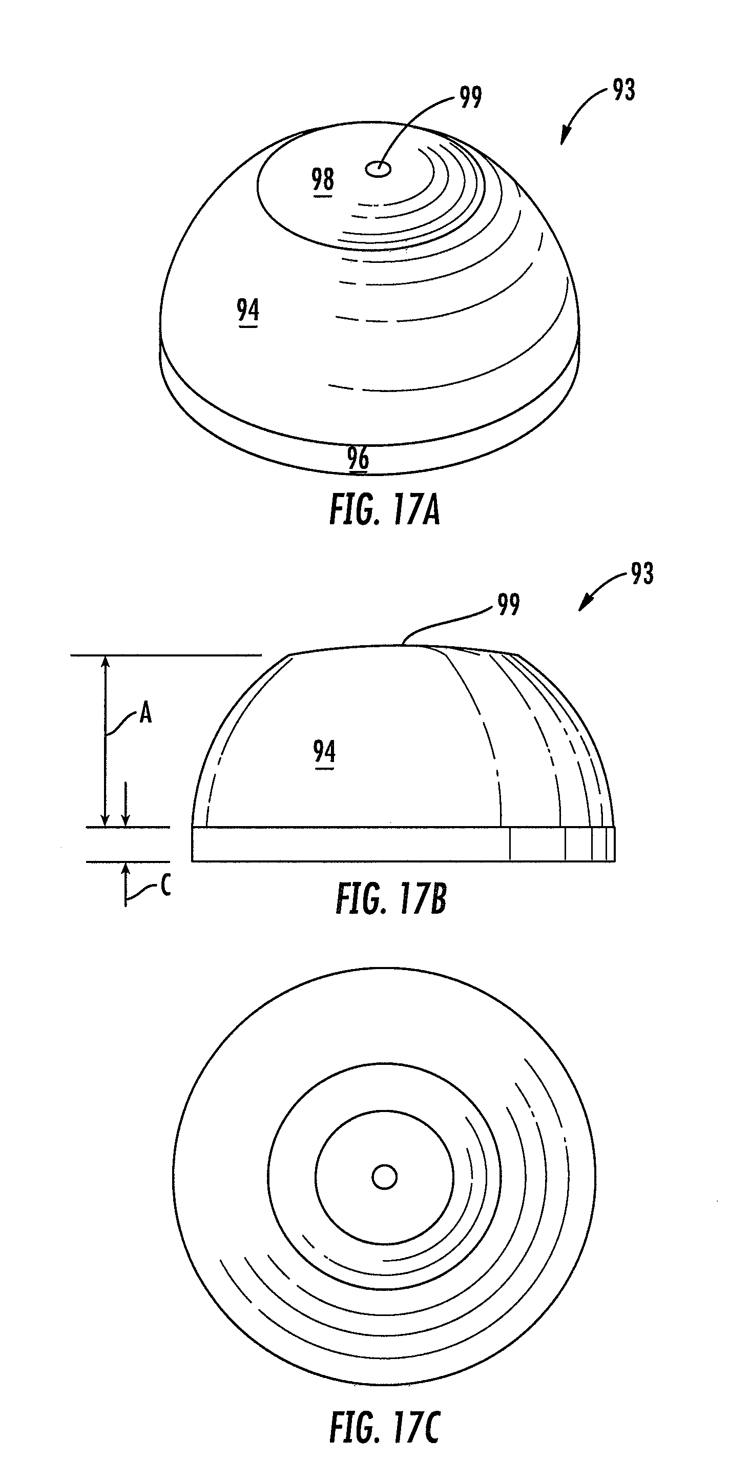
D00014

D00015

D00016

D00017
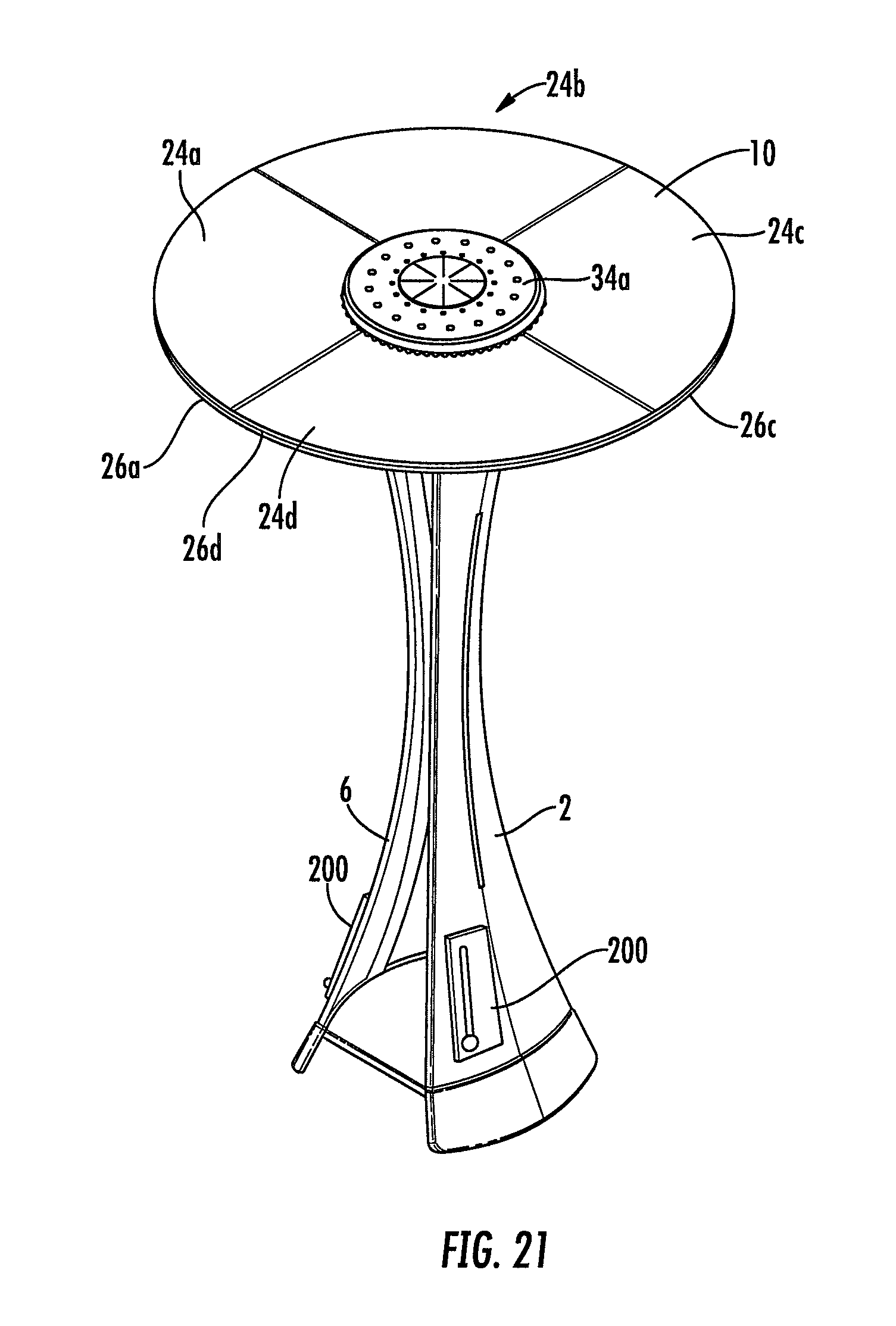
D00018
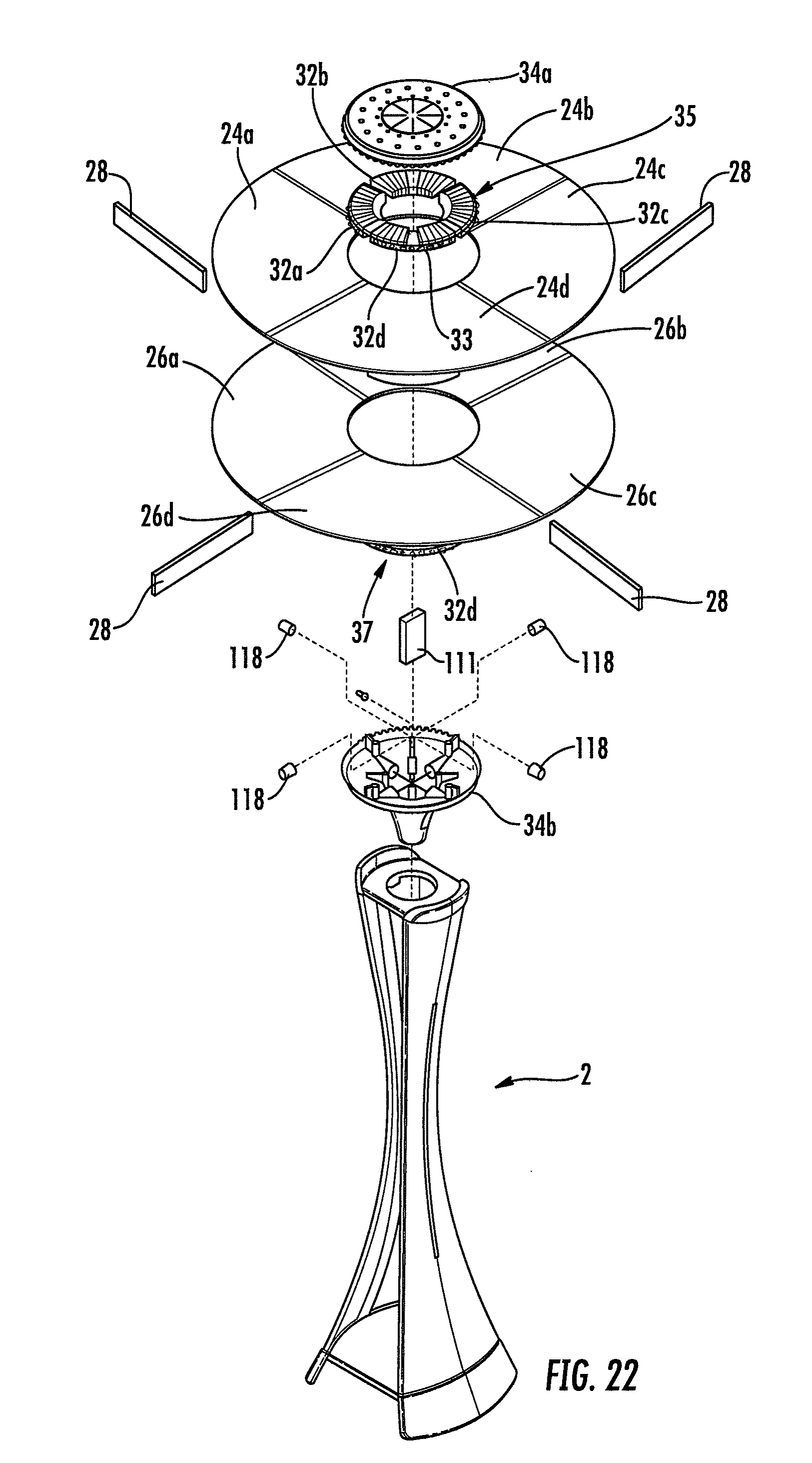
D00019

D00020
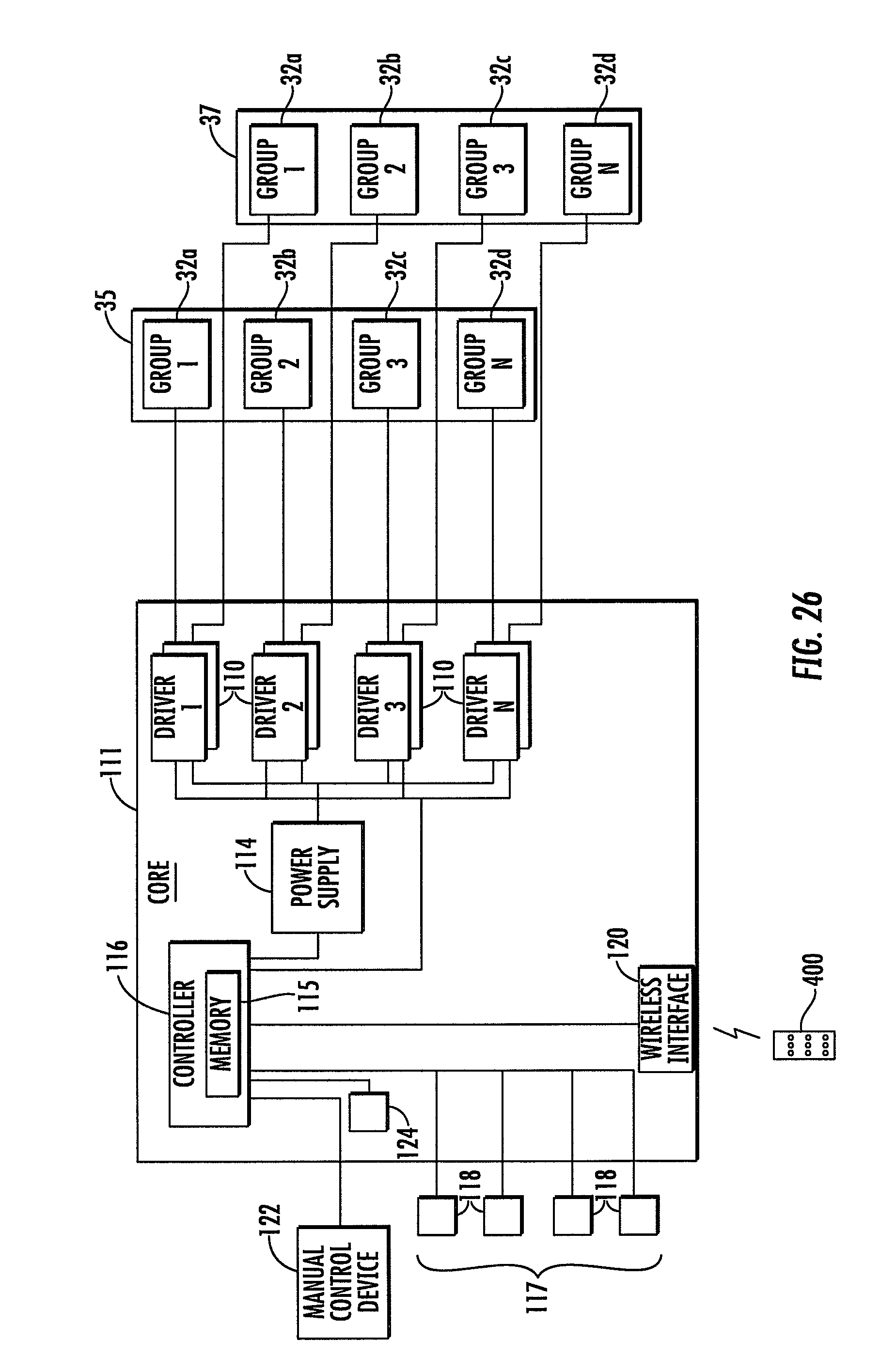
XML
uspto.report is an independent third-party trademark research tool that is not affiliated, endorsed, or sponsored by the United States Patent and Trademark Office (USPTO) or any other governmental organization. The information provided by uspto.report is based on publicly available data at the time of writing and is intended for informational purposes only.
While we strive to provide accurate and up-to-date information, we do not guarantee the accuracy, completeness, reliability, or suitability of the information displayed on this site. The use of this site is at your own risk. Any reliance you place on such information is therefore strictly at your own risk.
All official trademark data, including owner information, should be verified by visiting the official USPTO website at www.uspto.gov. This site is not intended to replace professional legal advice and should not be used as a substitute for consulting with a legal professional who is knowledgeable about trademark law.