Microelectromechanical systems and method of manufacturing the same
Bae , et al. Sept
U.S. patent number 10,407,298 [Application Number 15/663,646] was granted by the patent office on 2019-09-10 for microelectromechanical systems and method of manufacturing the same. This patent grant is currently assigned to ADVANCED SEMICONDUCTOR ENGINEERING KOREA, INC.. The grantee listed for this patent is Advanced Semiconductor Engineering Korea, Inc.. Invention is credited to Soonheung Bae, Dukyung Kim, Kyunghwan Sul, Hoguen Yoon.


| United States Patent | 10,407,298 |
| Bae , et al. | September 10, 2019 |
Microelectromechanical systems and method of manufacturing the same
Abstract
The present disclosure relates to an electronic device. The electronic device comprises a substrate, a micro-electromechanical systems (MEMS) device and an attachment element. The substrate defines an opening penetrating the substrate. The MEMS device has an active surface facing away from the substrate and a sensing region facing toward the opening. The attachment element is disposed on the substrate and surrounding the opening and the sensing region of the MEMS device.
| Inventors: | Bae; Soonheung (Paju-Si, KR), Yoon; Hoguen (Paju-Si, KR), Sul; Kyunghwan (Paju-Si, KR), Kim; Dukyung (Paju-Si, KR) | ||||||||||
|---|---|---|---|---|---|---|---|---|---|---|---|
| Applicant: |
|
||||||||||
| Assignee: | ADVANCED SEMICONDUCTOR ENGINEERING
KOREA, INC. (Paju-si, KR) |
||||||||||
| Family ID: | 65138695 | ||||||||||
| Appl. No.: | 15/663,646 | ||||||||||
| Filed: | July 28, 2017 |
Prior Publication Data
| Document Identifier | Publication Date | |
|---|---|---|
| US 20190031501 A1 | Jan 31, 2019 | |
| Current U.S. Class: | 1/1 |
| Current CPC Class: | B81B 7/0048 (20130101); H01L 29/84 (20130101); B81B 7/0061 (20130101); B81C 3/001 (20130101); B81B 2201/0257 (20130101); H01L 23/02 (20130101) |
| Current International Class: | B81B 7/00 (20060101); H01L 29/84 (20060101); H01L 23/02 (20060101) |
References Cited [Referenced By]
U.S. Patent Documents
| 6713864 | March 2004 | Huang |
| 7675180 | March 2010 | St. Amand |
| 7875942 | January 2011 | Cortese |
| 7898043 | March 2011 | Ziglioli |
| 7998774 | August 2011 | Ziglioli |
| 8043881 | October 2011 | Cortese |
| 8546895 | October 2013 | Cortese |
| 8618619 | December 2013 | Miks |
| 9013011 | April 2015 | Kuo |
| 9475691 | October 2016 | Chua |
| 9613877 | April 2017 | Suthiwongsunthorn |
| 9701534 | July 2017 | Lin |
| 9758372 | September 2017 | Kuo |
| 2007/0040231 | February 2007 | Harney |
| 2008/0150104 | June 2008 | Zimmerman |
| 2008/0164543 | July 2008 | Ziglioli |
| 2008/0179697 | July 2008 | Cortese |
| 2009/0218668 | September 2009 | Zhe |
| 2010/0090295 | April 2010 | Zhe |
| 2010/0284553 | November 2010 | Conti |
| 2011/0005326 | January 2011 | Bentley |
| 2012/0032285 | February 2012 | Cortese |
| 2013/0069180 | March 2013 | Umeda |
| 2013/0129133 | May 2013 | Inoda |
| 2013/0223023 | August 2013 | Dehe |
| 2014/0003632 | January 2014 | Reinisch |
| 2014/0084396 | March 2014 | Jenkins |
| 2015/0041931 | February 2015 | Szczech |
| 2015/0102478 | April 2015 | Suthiwongsunthorn |
| 2016/0167948 | June 2016 | Holliday |
| 2016/0214857 | July 2016 | Lin |
| 2016/0276545 | September 2016 | Mueller |
| 2017/0217760 | August 2017 | Piechocinski |
| 2017/0217762 | August 2017 | Hoekstra |
| 2017/0247249 | August 2017 | Duqi |
| 2017/0260043 | September 2017 | Lin |
| 2017/0275152 | September 2017 | Ziglioli |
| 2017/0294401 | October 2017 | Suthiwongsunthorn |
| 3210934 | Aug 2017 | EP | |||
| 2546830 | Aug 2017 | GB | |||
Attorney, Agent or Firm: Foley & Lardner LLP Liu; Cliff Z.
Claims
What is claimed is:
1. An electronic device, comprising: a substrate defining an opening penetrating the substrate; a microelectromechanical systems (MEMS) device having an active surface facing away from the substrate and a sensing region facing toward the opening; an attachment element disposed on the substrate and surrounding the opening and the sensing region of the MEMS device; a die disposed on the substrate; a package body covering the die and exposing the MEMS device; and a metal lid disposed on the package body, wherein the metal lid defines an opening exposing the MEMS device, wherein the attachment element includes a B-stage silicon soft adhesive material, and the package body defines a cavity to accommodate the MEMS device, and a sidewall of the cavity includes a protrusion portion.
2. An electronic device, comprising: a substrate having a first surface and a second surface opposite to the first surface, the substrate defining an opening penetrating the substrate and a recess on the first surface of the substrate; a microelectromechanical systems (MEMS) device having an active surface facing away from the substrate and a sensing region facing toward the opening; and an attachment element surrounding the opening and the sensing region of the MEMS device, wherein a portion of the attachment element is within the recess.
3. The electronic device of claim 2, wherein the sensing region is substantially aligned with the opening.
4. The electronic device of claim 2, further comprising: a die disposed on the substrate; a package body covering the die and exposing the MEMS device; and a metal lid disposed on the package body, wherein the metal lid defines an opening exposing the MEMS device.
5. The electronic device of claim 4, wherein the package body defines a cavity to accommodate the MEMS device, and a sidewall of the cavity includes a protrusion portion.
6. An electronic device, comprising: a substrate defining an opening penetrating the substrate; a microelectromechanical systems (MEMS) device having an active surface facing away from the substrate and a sensing region facing toward the opening; a support bar disposed between the MEMS device and the substrate, the support bar surrounding the opening of the substrate; and an attachment element surrounding the support bar.
7. The electronic device of claim 6, wherein a portion of the attachment element is between the support bar and the MEMS device.
8. The electronic device of claim 6, where the sensing region is substantially aligned with the opening.
9. The electronic device of claim 6, further comprising: a die disposed on the substrate; a package body covering the die and exposing the MEMS device; and a metal lid disposed on the package body, wherein the metal lid defines an opening exposing the MEMS device.
10. The electronic device of claim 9, wherein the package body defines a cavity to accommodate the MEMS device, and a sidewall of the cavity includes a protrusion portion.
Description
BACKGROUND
1. Technical Field
The present disclosure relates to a semiconductor package device including a microelectromechanical system (MEMS) and method of manufacturing the same.
2. Description of the Related Art
MEMS (as used herein, the term "MEMS" may be used to refer to a singular microelectromechanical system or to a plurality of microelectromechanical systems) can be used in semiconductor devices to detect a signal (such as sound, movement or motion, pressure, gas, humidity, temperature, and the like) and to transform the detected signal to an electrical signal. Semiconductor devices (e.g., semiconductor devices using MEMS) have become progressively more complex. The trend is driven at least in part by the demand for smaller sizes and enhanced processing speeds. At the same time, there is a demand to further miniaturize many electronic products containing these semiconductor devices. It may be desirable in some cases to reduce the space occupied by MEMS on a substrate of a semiconductor device, and to simplify and combine packaging, board manufacturing, and assembly processes applicable to the semiconductor device and the substrate.
In a comparative MEMS pressure sensor package, a MEMS die is usually connected to the substrate by flip-chip technique. However, due to the inconsistent diameters of solder balls, the MEMS die may tilt, which may reduce the performance of the MEMS die. In addition, the adhesive applied between the MEMS die and the substrate may flow into a sensing opening (penetrating the substrate), which may also affect the performance of the MEMS pressure sensor.
SUMMARY
In some embodiments, according to one aspect of the present disclosure, an electronic device comprises a substrate, a micro-electromechanical systems (MEMS) device and an attachment element. The substrate defines an opening penetrating the substrate. The MEMS device has an active surface facing away from the substrate and a sensing region facing toward the opening. The attachment element is disposed on the substrate and surrounding the opening and the sensing region of the MEMS device.
In some embodiments, according to one aspect of the present disclosure, an electronic device comprises a substrate, a MEMS device and an attachment element. The substrate has a first surface and a second surface opposite to the first surface. The substrate defines an opening penetrating the substrate and a recess on the first surface of the substrate. The MEMS device has an active surface facing away from the substrate and a sensing region facing toward the opening. The attachment element surrounds the opening and the sensing region of the MEMS device. A portion of the attachment element is within the recess.
In some embodiments, according to one aspect of the present disclosure, an electronic device comprises a substrate, a MEMS device, a support bar and an attachment element. The substrate defines an opening penetrating the substrate. The MEMS device has an active surface facing away from the substrate and a sensing region facing toward the opening. The support bar is disposed between the MEMS device and the substrate. The support bar surrounds the opening of the substrate. The attachment element surrounds the support bar.
BRIEF DESCRIPTION OF THE DRAWINGS
FIG. 1A illustrates a cross-sectional view of a semiconductor package device in accordance with some embodiments of the present disclosure;
FIG. 1B illustrates a bottom view of a semiconductor package device in accordance with some embodiments of the present disclosure;
FIG. 2A illustrates a cross-sectional view of a semiconductor package device in accordance with some embodiments of the present disclosure;
FIG. 2B illustrates a bottom view of a semiconductor package device in accordance with some embodiments of the present disclosure;
FIG. 2C illustrates one or more types of stage of the semiconductor package device of FIG. 2B in accordance with some embodiments of the present disclosure;
FIG. 2D illustrates one or more types of stage of the semiconductor package device of FIG. 2B in accordance with some embodiments of the present disclosure;
FIG. 2E illustrates one or more types of stage of the semiconductor package device of FIG. 2B in accordance with some embodiments of the present disclosure;
FIG. 3A illustrates a cross-sectional view of a semiconductor package device in accordance with some embodiments of the present disclosure;
FIG. 3B illustrates a bottom view of a semiconductor package device in accordance with some embodiments of the present disclosure;
FIG. 4A illustrates a cross-sectional view of a semiconductor package device in accordance with some embodiments of the present disclosure; and
FIG. 4B illustrates a bottom perspective view of a semiconductor package device in accordance with some embodiments of the present disclosure.
Common reference numerals are used throughout the drawings and the detailed description to indicate the same or similar elements. The present disclosure will be readily understood from the following detailed description taken in conjunction with the accompanying drawings.
DETAILED DESCRIPTION
FIG. 1A illustrates a semiconductor package device 1 in accordance with some embodiments of the present disclosure. The semiconductor package device 1 includes a substrate 10, a MEMS device 11 (or abbreviated as MEMS 11), an attachment element 12, an electronic component 13, a package body 14 and a metal lid 15.
The substrate 10 may be, for example, a printed circuit board (PCB), such as a paper-based copper foil laminate, a composite copper foil laminate, a polymer-impregnated glass-fiber-based copper foil laminate, or a combination of two or more thereof. The substrate 10 may include an interconnection structure, such as a redistribution layer (RDL) or a grounding element. The substrate 10 has a surface 101 and a surface 102 opposite to the surface 101. In some embodiments, the surface 101 of the substrate 10 is referred to as a top surface or a first surface, and the surface 102 of the substrate 10 is referred to as a bottom surface or a second surface. The substrate 10 defines an opening 10h penetrating the substrate 10.
The MEMS 11 is disposed on the substrate 10 and across the opening 10h of the substrate 10. The MEMS has an active surface (also referred to as active side) 111 facing away the substrate 10 and a back surface (also referred to as back side) 112 opposite to the active surface 111. In some embodiments, the MEMS 11 includes a sensing region (also referred to as sensing region) 11s on the back surface 112 of the MEMS 11 to receive at least one physical signal from environment (e.g., sound, pressure, temperature, humidity, gas, and the like) and to convert the received physical signal to an electrical signal (e.g., for subsequent processing). In some embodiments, the MEMS 11 can be, e.g., a pressure sensor, a microphone, a barometer, a thermometer, a hygrometer, a gas detector, and the like. The sensing region 11s of the MEMS 11 faces toward the opening 10h of the substrate 10. In some embodiments, the sensing region 11s of the MEMS 11 is substantially aligned with the opening 10h of the substrate 10, such that any displacement between a center of the sensing region 11s and a center of the opening 10h is no greater than 1 .mu.m, no greater than 5 .mu.m, or no greater than 10 .mu.m. In some embodiments, the MEMS 11 is electrically connected to the substrate 10 through one or more bonding wires.
The attachment element 12 is disposed between the substrate 10 and the MEMS 11 to attach the MEMS to the substrate 10. That is, the attachment element 12 is disposed between the top surface 101 of the substrate 10 and the back surface 112 of the MEMS 11. As shown in FIG. 1A and FIG. 1B, which illustrates a bottom view of the semiconductor package device 1 in FIG. 1A, the attachment 12 surrounds the opening 10h of the substrate 10 and the sensing region 11s of the MEMS 11. In some embodiments, the material of the attachment element 12 is selected to absorb mechanical stress between the MEMS 11 and the substrate 10. For example, the attachment element 12 is selected from silicon soft adhesive material, B-stage silicon soft adhesive material, other elastomeric material, or a combination thereof.
The electronic component 13 is disposed on the top surface 101 of the substrate 10. The electronic component 13 may be an active component, such as an integrated circuit (IC) chip or a die. In some embodiments, the electronic component 13 may be an application-specific integrated circuit (ASIC). The electronic component 13 may be electrically connected to the top surface 101 of the substrate 10 by way of flip-chip or wire-bond techniques.
The package body 14 is disposed on at least a portion of the top surface 101 of the substrate 10 to cover or encapsulate the electronic component 13. The MEMS 11 and the attachment element 12 are exposed from the package body 14. For example, the package body 14 may define a cavity to accommodate the MEMS 111. As shown in FIG. 1A, a sidewall 141 of the cavity may include a protrusion portion 14p. In some embodiments, the package body 14 includes, e.g., an epoxy resin having fillers, a molding compound (e.g., an epoxy molding compound or other molding compound), a polyimide, a phenolic compound or material, a material with a silicone dispersed therein, or a combination of two or more thereof.
The metal lid 15 is disposed on the package body 14. The metal lid 15 defines a hole 15h to expose the MEMS 11. In some embodiments, the metal lid 15 is a conductive thin film, and may include, for example, aluminum (Al), copper (Cu), chromium (Cr), tin (Sn), gold (Au), silver (Ag), nickel (Ni) or stainless steel, another metal, or a mixture, an alloy, or other combination of two of more thereof. The metal lid 15 can provide electromagnetic interference (EMI) shielding for the electronic component 13 and the MEMS 11.
In a comparative MEMS package, a MEMS die is usually connected to the substrate by flip-chip technique. However, due to the inconsistent diameters of solder balls, the MEMS die may tilt, which may reduce the performance of the MEMS die. In addition, the adhesive applied between the MEMS die and the substrate may flow into a sensing opening (penetrating the substrate), which may also affect the performance of the MEMS die. In accordance with the embodiments shown in FIGS. 1A and 1B, by using wire bonding technique to connect the MEMS 11 to the substrate 10, the tilt issue of the MEMS 11 can be solved. In addition, a robust dam bar (e.g., attachment element 12) disposed around the sensing opening (e.g., the opening 10h of the substrate 10) can prevent the adhesive from flowing into the sensing hole and release the mechanical stress between the MEMS 11 and the substrate 10.
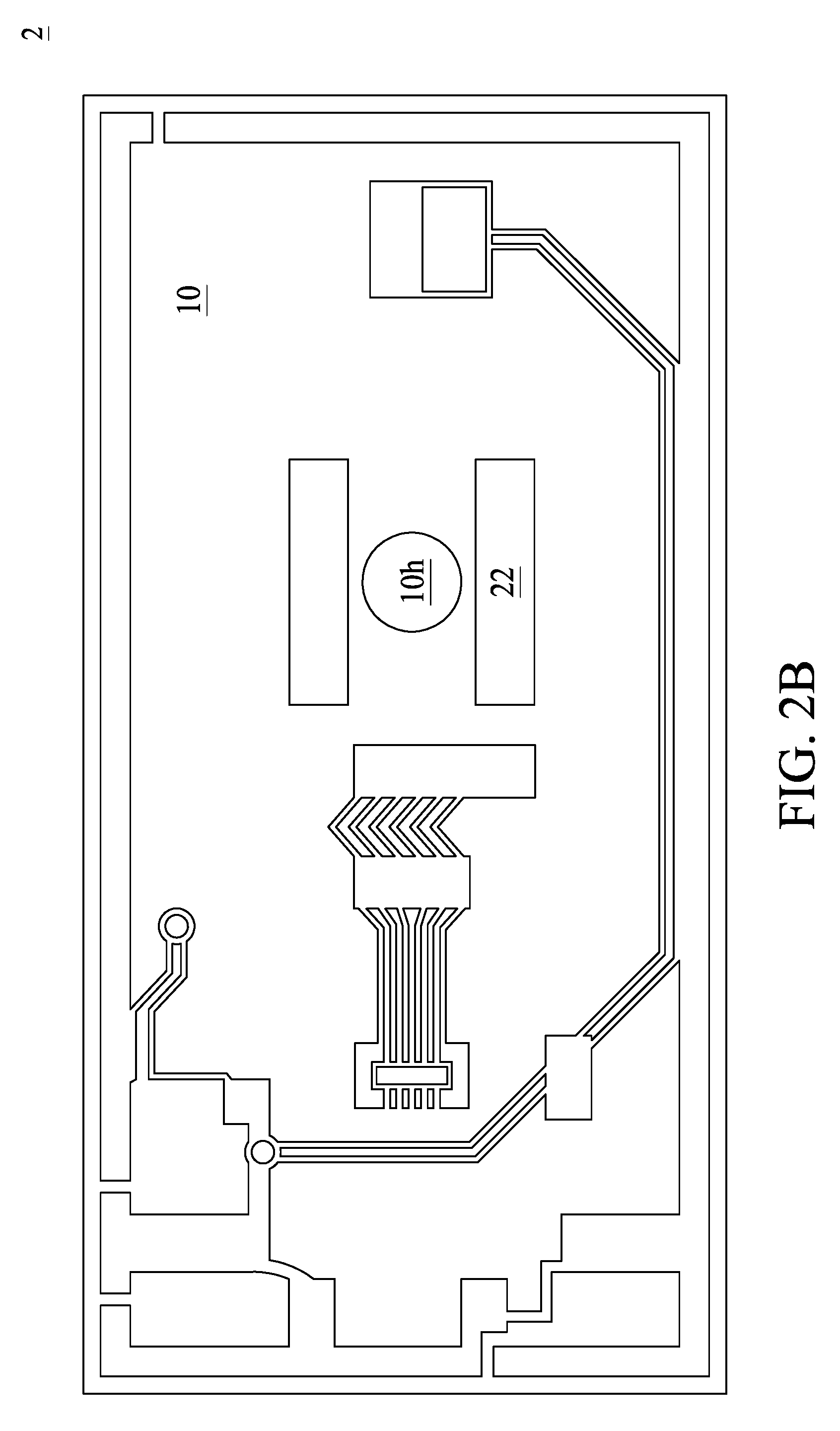
FIG. 2A illustrates a semiconductor package device 2 in accordance with some embodiments of the present disclosure. The semiconductor package device 2 is similar to the semiconductor package device 1 shown in FIG. 1A except that the semiconductor package device 2 further includes a stage 22.
The stage 22 is disposed on the substrate 10 and between the MEMS 11 and the substrate 10. In some embodiments, a portion of the attachment element 12 is disposed between the MEMS 11 and the stage 22. In some embodiments, a thickness of the attachment element 12 is greater than a thickness of the stage 22. For example, the thickness of the attachment element 12 is about 100 micrometer (.mu.m) while the thickness of the stage 22 is about 30 .mu.m. In some embodiments, the stage 22 is formed of, or includes, solder resist. In some embodiments, the attachment element 12 may be formed of, or include, one or more soft adhesive materials. For example, the attachment element 12 may be in a liquid form and dispensed on the substrate 10.
In accordance with the embodiments shown in FIGS. 2A and 1B, control over the thickness of the attachment element 12 is facilitated when a support structure (e.g., stage 22) is disposed between the substrate 10 and the adhesive element 12, because the stage 22 can have less tolerance in thickness in case that the attachment element 12 is relatively thick.
As shown in FIG. 2B, which illustrates a bottom view of the semiconductor package device 2 in FIG. 2A, the stage 22 is adjacent to the opening 10h. In some embodiments, the stage 22 is in a shape of, e.g., multiple parallel bars (e.g., two parallel bars as shown in FIG. 2C), an L-shaped bar (as shown in FIG. 2D) or multiple blocks (e.g., four blocks as shown in FIG. 2E) on four edges of the MEMS 11.
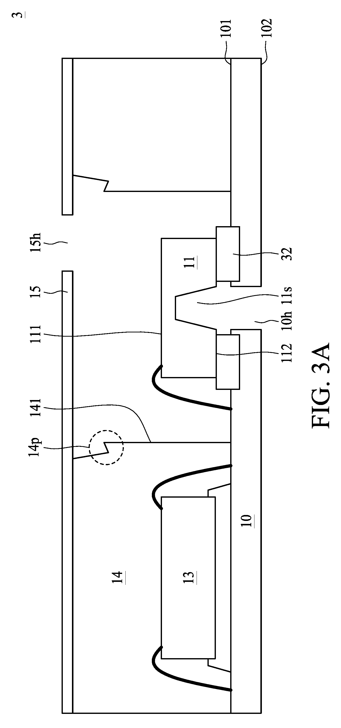
FIG. 3A illustrates a semiconductor package device 3 in accordance with some embodiments of the present disclosure. The semiconductor package device 3 is similar to the semiconductor package device 1 shown in FIG. 1A except that in the semiconductor package device 2, a portion of the attachment element 32 is within the substrate 10.
The substrate 10 has a recess on the first surface 101 of the substrate 10. The recess is adjacent to and surrounds the opening 10h of the substrate 10. At least a portion of the attachment element 32 is disposed within the recess of the substrate 10. Therefore, as shown in FIG. 3B, which illustrates a bottom view of the semiconductor package device 3 in FIG. 3A, the attachment element 32 surrounds the opening 10h of the substrate 10. Forming the recess around the opening 10h of the substrate 10 can prevent the attachment element 12 from flowing into the opening 10h.
FIG. 4A illustrates a semiconductor package device 4 in accordance with some embodiments of the present disclosure. The semiconductor package device 4 is similar to the semiconductor package device 2 shown in FIG. 2A except that the stage 46 of the semiconductor package device 4 is formed of epoxy and formed by inkjet dispensing. The attachment element 42 is disposed between the MEMS 11 and the stage 46. As shown in FIG. 4B, which illustrates a bottom view of the semiconductor package device 4 in FIG. 4, the stage 46 surrounds the opening 10h of the substrate 10. In some embodiments, the stage 46 may be in a shape of, e.g., a circle or a square.
As used herein, the terms "conductive," "electrically conductive" and "electrical conductivity" refer to an ability to transport an electric current. Electrically conductive materials typically indicate those materials that exhibit little or no opposition to the flow of an electric current. One measure of electrical conductivity is Siemens per meter (S/m). Typically, an electrically conductive material is one having a conductivity greater than approximately 10.sup.4 S/m, such as at least 10.sup.5 S/m or at least 10.sup.6 S/m. The electrical conductivity of a material can sometimes vary with temperature. Unless otherwise specified, the electrical conductivity of a material is measured at room temperature.
As used herein, the terms "substantially," "substantial," "approximately," and "about" are used to describe and account for small variations. When used in conjunction with an event or circumstance, the terms can refer to instances in which the event or circumstance occurs precisely as well as instances in which the event or circumstance occurs to a close approximation. For example, when used in conjunction with a numerical value, the terms can refer to a range of variation of less than or equal to .+-.10% of that numerical value, such as less than or equal to .+-.5%, less than or equal to .+-.4%, less than or equal to .+-.3%, less than or equal to .+-.2%, less than or equal to .+-.1%, less than or equal to .+-.0.5%, less than or equal to .+-.0.1%, or less than or equal to .+-.0.05%. For example, two numerical values can be deemed to be "substantially" the same or equal if a difference between the values is less than or equal to .+-.10% of an average of the values, such as less than or equal to .+-.5%, less than or equal to .+-.4%, less than or equal to .+-.3%, less than or equal to .+-.2%, less than or equal to .+-.1%, less than or equal to .+-.0.5%, less than or equal to .+-.0.1%, or less than or equal to .+-.0.05%. For example, "substantially" parallel can refer to a range of angular variation relative to 0.degree. that is less than or equal to .+-.10.degree., such as less than or equal to .+-.5.degree., less than or equal to .+-.4.degree., less than or equal to .+-.3.degree., less than or equal to .+-.2.degree., less than or equal to .+-.1.degree., less than or equal to .+-.0.5.degree., less than or equal to .+-.0.1.degree., or less than or equal to .+-.0.05.degree.. For example, "substantially" perpendicular can refer to a range of angular variation relative to 90.degree. that is less than or equal to .+-.10.degree., such as less than or equal to .+-.5.degree., less than or equal to .+-.4.degree., less than or equal to .+-.3.degree., less than or equal to .+-.2.degree., less than or equal to .+-.1.degree., less than or equal to .+-.0.5.degree., less than or equal to .+-.0.1.degree., or less than or equal to .+-.0.05.degree..
In some embodiments, two surfaces can be deemed to be coplanar or substantially coplanar if a displacement between the surfaces is small, such as no greater than 1 .mu.m, no greater than 5 .mu.m, or no greater than 10 .mu.m.
Additionally, amounts, ratios, and other numerical values are sometimes presented herein in a range format. It is to be understood that such a range format is used for convenience and brevity and should be understood flexibly to include numerical values explicitly specified as limits of a range, but also to include all individual numerical values or sub-ranges encompassed within that range as if each numerical value and sub-range is explicitly specified.
While the present disclosure has been described and illustrated with reference to specific embodiments thereof, these descriptions and illustrations do not limit the present disclosure. It should be understood by those skilled in the art that various changes may be made and equivalents may be substituted without departing from the true spirit and scope of the present disclosure as defined by the appended claims. The illustrations may not be necessarily be drawn to scale. There may be distinctions between the artistic renditions in the present disclosure and the actual apparatus due to manufacturing processes and tolerances. There may be other embodiments of the present disclosure which are not specifically illustrated. The specification and drawings are to be regarded as illustrative rather than restrictive. Modifications may be made to adapt a particular situation, material, composition of matter, method, or process to the objective, spirit and scope of the present disclosure. All such modifications are intended to be within the scope of the claims appended hereto. While the methods disclosed herein have been described with reference to particular operations performed in a particular order, it will be understood that these operations may be combined, sub-divided, or re-ordered to form an equivalent method without departing from the teachings of the present disclosure. Accordingly, unless specifically indicated herein, the order and grouping of the operations are not limitations of the present disclosure.
* * * * *
D00000
D00001
D00002
D00003
D00004
D00005
D00006
D00007
D00008
D00009
XML
uspto.report is an independent third-party trademark research tool that is not affiliated, endorsed, or sponsored by the United States Patent and Trademark Office (USPTO) or any other governmental organization. The information provided by uspto.report is based on publicly available data at the time of writing and is intended for informational purposes only.
While we strive to provide accurate and up-to-date information, we do not guarantee the accuracy, completeness, reliability, or suitability of the information displayed on this site. The use of this site is at your own risk. Any reliance you place on such information is therefore strictly at your own risk.
All official trademark data, including owner information, should be verified by visiting the official USPTO website at www.uspto.gov. This site is not intended to replace professional legal advice and should not be used as a substitute for consulting with a legal professional who is knowledgeable about trademark law.