Magnetic write transducer with first and second pole sections
Bance , et al. A
U.S. patent number 10,388,307 [Application Number 15/956,855] was granted by the patent office on 2019-08-20 for magnetic write transducer with first and second pole sections. This patent grant is currently assigned to Seagate Technology LLC. The grantee listed for this patent is Seagate Technology LLC. Invention is credited to Simon Bance, Choon How Gan, Mark Anthony Gubbins.


| United States Patent | 10,388,307 |
| Bance , et al. | August 20, 2019 |
Magnetic write transducer with first and second pole sections
Abstract
A recording head has a magnetic write transducer proximate a side of a plasmonic gap waveguide. The magnetic write transducer has a first write pole section that tapers in a crosstrack direction and downtrack direction to form a tapered tip. The first write pole section includes a high-moment, seed layer on one side. A second write pole section is coupled to the first write pole section. The second write pole section extends a second distance away from the media-facing surface less than that of the first write pole section. A tip of the second write pole section is tapered in the crosstrack and downtrack directions.
| Inventors: | Bance; Simon (St. Albans, GB), Gan; Choon How (Derry, GB), Gubbins; Mark Anthony (Letterkenny, IE) | ||||||||||
|---|---|---|---|---|---|---|---|---|---|---|---|
| Applicant: |
|
||||||||||
| Assignee: | Seagate Technology LLC
(Cupertino, CA) |
||||||||||
| Family ID: | 67620717 | ||||||||||
| Appl. No.: | 15/956,855 | ||||||||||
| Filed: | April 19, 2018 |
Related U.S. Patent Documents
| Application Number | Filing Date | Patent Number | Issue Date | ||
|---|---|---|---|---|---|
| 62487642 | Apr 20, 2017 | ||||
| Current U.S. Class: | 1/1 |
| Current CPC Class: | G11B 5/3116 (20130101); G11B 5/6088 (20130101); G11B 2005/0021 (20130101) |
| Current International Class: | G11B 5/31 (20060101); G11B 5/60 (20060101); G11B 5/00 (20060101) |
References Cited [Referenced By]
U.S. Patent Documents
| 6029334 | February 2000 | Hartley |
| 8264792 | September 2012 | Bai et al. |
| 8310901 | November 2012 | Batra |
| 8537494 | September 2013 | Pan |
| 8873351 | October 2014 | Aoki |
| 9019659 | April 2015 | Yin et al. |
| 9218841 | December 2015 | Moriya |
| 9721591 | August 2017 | Liu |
| 10106885 | October 2018 | Tanner |
| 10115416 | October 2018 | Liu |
| 10204644 | February 2019 | Benakli et al. |
| 2006/0262453 | November 2006 | Mochizuki |
| 2011/0222188 | September 2011 | Etoh et al. |
| 2011/0273800 | November 2011 | Takano et al. |
| 2014/0063648 | March 2014 | Shiroishi et al. |
| 2014/0285919 | September 2014 | Tanaka et al. |
| 2015/0235658 | August 2015 | Cao |
| 2016/0225390 | August 2016 | Saito |
| 2018/0137881 | May 2018 | Miyata |
| 2013004122 | Jan 2013 | JP | |||
Attorney, Agent or Firm: Hollingsworth Davis, LLC
Parent Case Text
RELATED PATENT DOCUMENTS
This application claims the benefit of Provisional Patent Application No. 62/487,642 filed on Apr. 20, 2017, which is incorporated herein by reference in its entirety.
Claims
What is claimed is:
1. A recording head, comprising: a plasmonic gap waveguide comprising first and second substrate-parallel sides offset downtrack from one another at a media-facing surface of the recording head; and a magnetic write transducer proximate the first substrate-parallel side of the plasmonic gap waveguide, the magnetic write transducer comprising: a first write pole section that tapers in a crosstrack direction and downtrack direction to form a tapered tip, the first write pole section extending a first distance away from the media-facing surface, a gap located between the tapered tip and the media-facing surface; and a second write pole section coupled to the first write pole section, the second write pole section extending a second distance away from the media-facing surface, the second distance being at least 1/5 that of the first distance, a tip of the second write pole section proximate the media-facing surface and tapered in the crosstrack direction and the downtrack direction.
2. The recording head of claim 1, wherein the first write pole section has a first crosstrack width away from the tapered tip that is at least 10 times larger than a corresponding second crosstrack width of the second write pole section that is away from the tip of the second write pole section.
3. The recording head of claim 1, wherein the first write pole section comprises a high-moment, seed layer on one substrate-parallel side.
4. The recording head of claim 3, wherein the magnetic write transducer further comprises a yoke facing the seed layer of the first write pole section, wherein an outline of the yoke on a substrate-parallel plane matches a corresponding outline of the first write pole section on the substrate-parallel plane.
5. The recording head of claim 4, wherein the yoke further comprise a taper that results in a narrowed downtrack dimension close to the tapered tip of the first write pole section.
6. The recording head of claim 1, wherein the tip of the second write pole section comprises a step that extends towards the plasmonic gap waveguide, the step providing heat sinking for the plasmonic gap waveguide.
7. The recording head of claim 1, wherein the plasmonic gap waveguide comprises a flared cavity that extends from the gap in a direction away from the media-facing surface.
8. The recording head of claim 7, wherein the plasmonic gap waveguide comprises a block of thermally robust material downtrack from the gap facing away from the magnetic write transducer.
9. The recording head of claim 1, further comprising a diffusion barrier between the plasmonic gap waveguide and the second write pole section.
10. A recording head, comprising: a plasmonic gap waveguide comprising first and second substrate-parallel sides offset downtrack from one another at a media-facing surface of the recording head; and a magnetic write transducer proximate the first substrate-parallel side of the plasmonic gap waveguide, the magnetic write transducer comprising: a first write pole section that tapers in a crosstrack direction and downtrack direction to form a tapered tip, the first write pole section extending a first distance away from the media-facing surface, a gap being located between the tapered tip and the media-facing surface; and a second write pole section coupled to the first write pole section, a tip of the second write pole section proximate the media-facing surface and tapered in the crosstrack direction and the downtrack direction, the tip of the second write pole section comprising a step that extends towards the plasmonic gap waveguide.
11. The recording head of claim 10, wherein second write pole section extends a second distance away from the media-facing surface, the second distance being at least 1/5 that of the first distance.
12. The recording head of claim 10, wherein the first write pole section has a first crosstrack width away from the tapered tip that is at least 10 times larger than a corresponding second crosstrack width of the second write pole section that is away from the tip of the second write pole section.
13. The recording head of claim 10, wherein the first write pole section comprises a high-moment, seed layer on one substrate-parallel side.
14. The recording head of claim 13, wherein the magnetic write transducer further comprises a yoke facing the seed layer of the first write pole section, wherein an outline of the yoke on a substrate-parallel plane matches a corresponding outline of the first write pole section on the substrate-parallel plane.
15. The recording head of claim 14, wherein the yoke further comprise a taper that results in a narrowed downtrack dimension close to the tapered tip of the first write pole section.
16. The recording head of claim 10, wherein the plasmonic gap waveguide comprises a flared cavity that extends from the gap in a direction away from the media-facing surface.
17. The recording head of claim 16, wherein the plasmonic gap waveguide comprises a block of thermally robust material downtrack from the gap facing away from the magnetic write transducer.
18. The recording head of claim 10, further comprising a diffusion barrier between the plasmonic gap waveguide and the second write pole section.
19. A recording head, comprising: a plasmonic gap waveguide comprising first and second substrate-parallel sides offset downtrack from one another at a media-facing surface of the recording head; and a magnetic write transducer proximate the first substrate-parallel side of the plasmonic gap waveguide, the magnetic write transducer comprising: a first write pole section that tapers in a crosstrack direction and downtrack direction to form a tapered tip, the first write pole section comprising a high-moment, seed layer on one substrate-parallel side, the first write pole section extending a first distance away from the media-facing surface, a gap located between the tapered tip and the media-facing surface; and a second write pole section coupled to the first wiite pole section, the second write pole section extending a second distance away from the media-facing surface, the second distance at least 1/5 that of the first distance, a tip of the second write pole section proximate the media-facing surface and tapered in the crosstrack direction and the downtrack direction, the tip of the second write pole section comprising a step that extends towards the plasmonic gap waveguide.
Description
SUMMARY
The present disclosure is directed to a magnetic write transducer with first and second pole sections. In one embodiment, a recording head has a plasmonic gap waveguide with first and second substrate-parallel sides offset downtrack from one another at a media-facing surface of the recording head. A magnetic write transducer is proximate the first substrate parallel side of the plasmonic gap waveguide. The magnetic write transducer includes a first write pole section that tapers in a crosstrack direction and downtrack direction to form a tapered tip. The first write pole section includes a high-moment, seed layer on one substrate-parallel side. The first write pole section extends a first distance away from the media-facing surface. A gap is located between the tapered tip and the media-facing surface.
The write transducer includes a second write pole section coupled to the first write pole section. The second write pole section extends a second distance away from the media-facing surface. The second distance is at least 1/5 that of the first distance. A tip of the second write pole section is located proximate the media facing surface and is tapered in the crosstrack direction and the downtrack direction.
These and other features and aspects of various embodiments may be understood in view of the following detailed discussion and accompanying drawings.
BRIEF DESCRIPTION OF THE DRAWINGS
The discussion below makes reference to the following figures, wherein the same reference number may be used to identify the similar/same component in multiple figures. Drawings are not necessarily to scale.
FIG. 1 is a perspective view of a slider assembly according to an example embodiment;
FIG. 2 is a cross-sectional view of read and write transducers according to example embodiments;
FIGS. 3 and 4 are respective side and perspective views of a magnetic write transducer according to an example embodiment;
FIGS. 5 and 6 are respective side and perspective views of a write pole according to example embodiments;
FIGS. 7A and 7B are a cross-sectional views of a write pole section and plasmonic gap waveguide according to an example embodiment;
FIGS. 8-11 are plan views showing dimensions of a magnetic write transducer according to an example embodiment;
FIGS. 12 and 13 are graphs showing magnetic field and temperature of a write transducer according to example embodiments; and
FIGS. 14 and 15 are saturation curves of a write transducer according to example embodiments.
DETAILED DESCRIPTION
The present disclosure generally relates to data storage devices that utilize magnetic storage media, e.g., disks. Data storage devices described herein use a particular type of magnetic data storage known heat-assisted magnetic recording (HAMR), also referred to as energy-assisted magnetic recording (EAMR), thermally-assisted magnetic recording (TAMR), and thermally-assisted recording (TAR). This technology uses an energy source such as a laser to create a small hotspot on a magnetic disk during recording. The heat lowers magnetic coercivity at the hotspot, allowing a write transducer to change magnetic orientation, after which the hotspot is allowed to rapidly cool. Due to the relatively high coercivity of the medium after cooling, the data is less susceptible to data errors due to thermally-induced, random fluctuation of magnetic orientation known as the superparamagnetic effect.
A HAMR device uses a near-field transducer to concentrate optical energy into a hotspot in a recording layer. The hotspot raises the media temperature locally, reducing the writing magnetic field required for high-density recording. A waveguide integrated into a read/write head delivers light to the near-field transducer and excites the near-field transducer. In response, the near-field transducer achieves surface plasmon resonance and tunnels a stream of surface plasmons to heat the recording medium. A magnetic transducer, which includes a magnetic write pole, applies a magnetic field to the hotspot, locally changing magnetic orientation within the hotspot, while regions outside the hotspot are not affected by the applied field. In the following disclosure below, a magnetic transducer is described that can increase magnetic field strength. This magnetic transducer is designed to work together with a particular near-field transducer to enable higher areal data density.
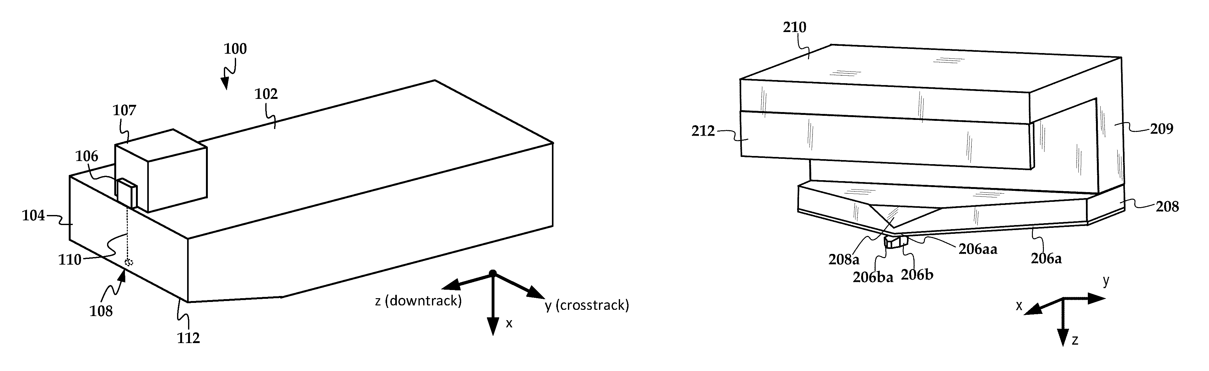
In reference now to FIG. 1, a perspective view shows a read/write head 100 according to an example embodiment. The read/write head 100 may be used in a magnetic data storage device, e.g., HAMR hard disk drive. The read/write head 100 may also be referred to herein interchangeably as a slider, write head, read head, recording head, etc. The read/write head 100 has a slider body 102 with read/write transducers at a trailing edge 104 that are held proximate to a surface of a magnetic recording medium (not shown), e.g., a magnetic disk.
The illustrated read/write head 100 is configured as a HAMR device, and so includes additional components that form a hot spot on the recording medium near the read/write transducer 108. These components include an energy source 106 (e.g., laser diode 106 mounted on submount 107) and a waveguide 110. The waveguide 110 delivers electromagnetic energy from the energy source 106 to a near-field transducer that is part of the read/write transducers 108. The near-field transducer achieves surface plasmon resonance in response and directs the energy out of a media-facing surface 112 to create a small hot spot on the recording medium.
In FIG. 2, a cross-sectional view of a slider shows details of the read/write transducers 108 according to an example embodiment. A read transducer 108a includes a read element 200 (e.g., magnetoresistive stack) located between shields 202-203. A magnetic write transducer 108b includes a coil 205 that, when energized, induces magnetic flux through a write pole 206, yoke 208, 209, a return pole 210, and shield 212. A near-field transducer (NFT) 214 is located at the media-facing surface 112 proximate the write pole 206. Light propagating through the waveguide causes the NFT 214 to achieve surface plasmon resonance.
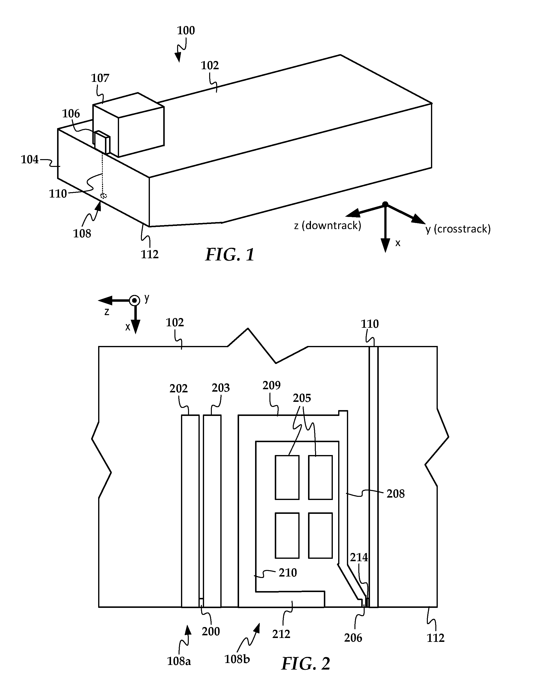
In FIGS. 3 and 4, respective side and perspective views show details of the magnetic write transducer 108a according to an example embodiment. As seen in these views, the write pole 206 has a first write pole section (WP1) 206a that tapers in a crosstrack direction and downtrack direction to form a tapered tip 206aa. The first write pole section 206a includes has a high-moment, seed layer on one substrate-parallel side facing the yoke 208. The first write pole section extends a first distance 300 away from the media-facing surface 112. A gap 302 is located between the tapered tip 206aa and the media-facing surface 112 and
A second write pole section 206b coupled to first write pole section 206a. The second write pole section 206b extends a second distance 304 away from the media-facing surface 112. The second distance at least 1/5 that of the first distance 300. A tip 206ba of the second write pole section is proximate the media facing surface 112 and tapered in the crosstrack direction and the downtrack direction (y- and z-directions in this figure).
As best seen in FIG. 4, the yoke 208 and the first write pole section 206a have matching outlines on a substrate-parallel plane (the xy-plane in these views). Therefore yoke 208 tapers in the crosstrack direction in the same amount as the first write pole section 206a. The yoke 208 also includes a taper 208a that results in a narrowed downtrack dimension close to the tip 206aa of the first write pole section 206a.
In FIGS. 5 and 6, respective side and perspective views show details of the second write pole section 206b according to an example embodiment. A top bevel 206bb increases field of the tapered tip 206ba. A step 206bc extends towards the near-field transducer and provides for increased heatsinking of the near-field transducer 214. Details of the near-field transducer 214 are seen in the cross-sectional view of FIG. 7.
As seen in FIGS. 7A and 7B, the near-field transducer 214 is configured as a plasmonic gap waveguide, and may be referred interchangeable herein as a near-field transducer or plasmonic gap waveguide. The near-field transducer 214 has a gap 214a with first and second substrate-parallel sides offset downtrack from one another at the media-facing surface 112. A flared cavity 214b extends from the gap 214a away from the media-facing surface 112. Light, as indicated by arrow 700, is coupled from the waveguide (not shown) to the flared cavity 214b. The near-field transducer 214 also includes a block 214c of a thermally robust material (e.g., Rh) at the media-facing surface 112 downtrack from the gap 214a and away from the write pole portion 206b. A diffusion barrier 702 formed of Ru separates the near-field transducer 214 from the second write pole section 206b.
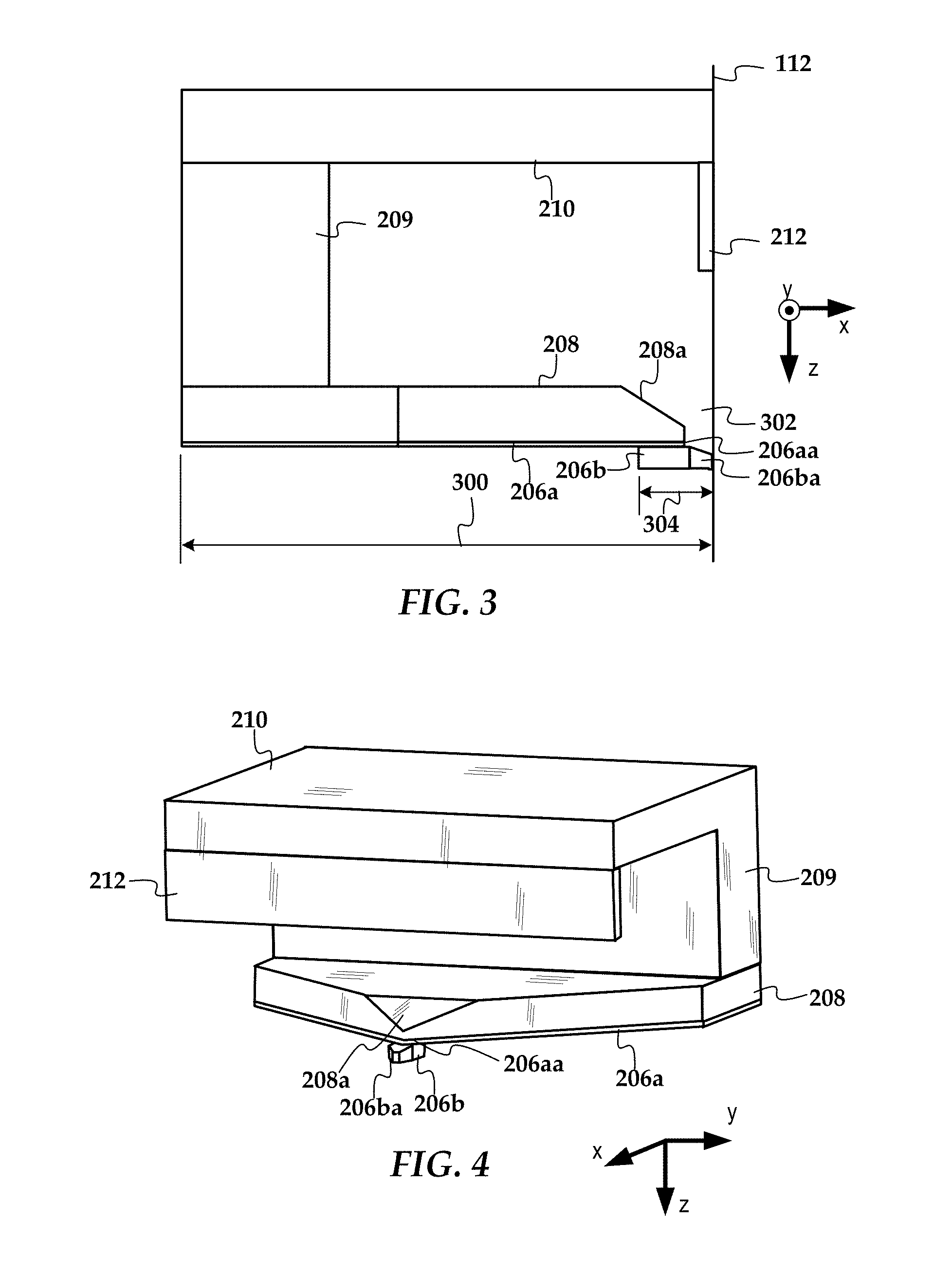
In FIGS. 8-9, side views show dimensions of the first and second write pole portions 206a-b and the yoke 208. In FIGS. 10 and 11, top view shows dimensions of these same components. In Tables 1-4 below, example values are provided for the dimensions shown in FIGS. 8-22, where WP2 refers to the first write pole portion and WP1 refers and second write pole portion.
TABLE-US-00001 TABLE 1 Dimensions shown in FIGS. 8-11 Name Units Value) Yoke_thickness nm 750 Yoke_BEV_a nm 1000 Yoke_BEV_b nm 550 WP2_length, Yoke_length nm 6900 WP2_thickness nm 80 WP2_recess, Yoke_recess nm 400 WP1_length nm 1000 WP1_thickness nm 300 WP1_FTBEV_a nm 300 WP1_FTBEV_b nm 90 WP1_scoop_a nm 950 WP1_scoop_b nm 10 WP2_recess, Yoke_recess nm 300 WP2_length, Yoke_length nm 6900 WP2_width, Yoke_width nm 10000 WP2_FA, Yoke_FA deg 52
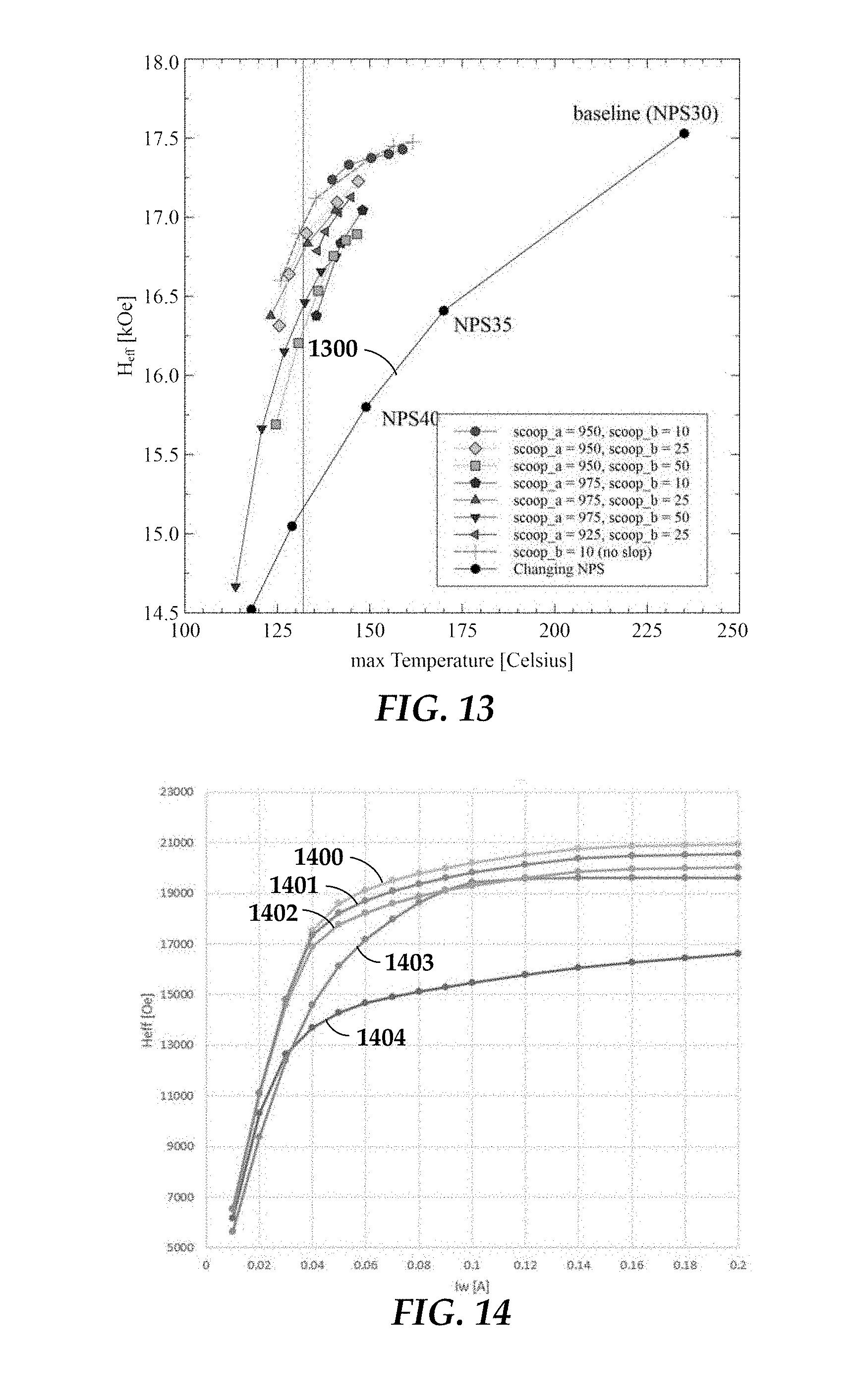
Analysis of the illustrated writer in FIGS. 3-11 shows effective field (H.sub.eff) of 19.4 kOe at 80 mA of coil current and perpendicular field (H.sub.perp) if 8.25 kOe at 80 mA. This represents an increase of effective field by as much as 28% over previous designs, and an increase in perpendicular field by as much as 33% over previous designs. In HAMR devices, the perpendicular field is believed to have the greatest impact on performance. In FIG. 12, a graph shows the variation in effective field and maximum temperature for different values of scoop_a, scoop_b, and slop shown in FIG. 9. The "slop" value indicates how angled the step 206bc where it extends from the second write pole section 206b. A value of slop=0 indicates that this intersection is a right angle. Note that for each set of points with the same scoop_a and scoop_b values, slop increases from left to right. At point 1200, slop=10 and this represents a good compromise between high field and low temperature.
In FIG. 13, a graph shows how decreasing the downtrack separation between the pole and the NFT affects temperature and effective field. This graphs shows performance of a baseline configuration, in which scoop_a=scoop_b=0. As indicated by the baseline curve 1300, the cutout that forms step 206bc enables a combination of high field and low temperature that cannot otherwise be obtained with this configuration.
In FIGS. 14 and 15, saturation curves show performance of various configurations of the write transducer described above. Curves 1400 and 1500 are for scoop_b=0; curves 1401 and 1501 are for the same design at 130.degree. C.; curves 1402 and 1502 are for the same design at 145.degree. C.; and curves 1403, 1404, 1503, and 1504 are for other designs currently in use. The illustrated embodiments saturate at a lower current than the previous designs, and so are likely well suited to higher data rates.
Unless otherwise indicated, all numbers expressing feature sizes, amounts, and physical properties used in the specification and claims are to be understood as being modified in all instances by the term "about." Accordingly, unless indicated to the contrary, the numerical parameters set forth in the foregoing specification and attached claims are approximations that can vary depending upon the desired properties sought to be obtained by those skilled in the art utilizing the teachings disclosed herein. The use of numerical ranges by endpoints includes all numbers within that range (e.g. 1 to 5 includes 1, 1.5, 2, 2.75, 3, 3.80, 4, and 5) and any range within that range.
The foregoing description of the example embodiments has been presented for the purposes of illustration and description. It is not intended to be exhaustive or to limit the embodiments to the precise form disclosed. Many modifications and variations are possible in light of the above teaching. Any or all features of the disclosed embodiments can be applied individually or in any combination are not meant to be limiting, but purely illustrative. It is intended that the scope of the invention be limited not with this detailed description, but rather determined by the claims appended hereto.
* * * * *
D00000
D00001
D00002
D00003
D00004
D00005
D00006
D00007
D00008
XML
uspto.report is an independent third-party trademark research tool that is not affiliated, endorsed, or sponsored by the United States Patent and Trademark Office (USPTO) or any other governmental organization. The information provided by uspto.report is based on publicly available data at the time of writing and is intended for informational purposes only.
While we strive to provide accurate and up-to-date information, we do not guarantee the accuracy, completeness, reliability, or suitability of the information displayed on this site. The use of this site is at your own risk. Any reliance you place on such information is therefore strictly at your own risk.
All official trademark data, including owner information, should be verified by visiting the official USPTO website at www.uspto.gov. This site is not intended to replace professional legal advice and should not be used as a substitute for consulting with a legal professional who is knowledgeable about trademark law.