Extremely stretchable electronics
Arora , et al. A
U.S. patent number 10,383,219 [Application Number 15/850,129] was granted by the patent office on 2019-08-13 for extremely stretchable electronics. This patent grant is currently assigned to MC10, Inc.. The grantee listed for this patent is MC10, Inc.. Invention is credited to William J. Arora, Roozbeh Ghaffari.


| United States Patent | 10,383,219 |
| Arora , et al. | August 13, 2019 |
Extremely stretchable electronics
Abstract
In embodiments, the present invention may attach at least two isolated electronic components to an elastomeric substrate, and arrange an electrical interconnection between the components in a boustrophedonic pattern interconnecting the two isolated electronic components with the electrical interconnection. The elastomeric substrate may then be stretched such that the components separate relative to one another, where the electrical interconnection maintains substantially identical electrical performance characteristics during stretching, and where the stretching may extend the separation distance between the electrical components to many times that of the unstretched distance.
| Inventors: | Arora; William J. (Bellevue, WA), Ghaffari; Roozbeh (Cambridge, MA) | ||||||||||
|---|---|---|---|---|---|---|---|---|---|---|---|
| Applicant: |
|
||||||||||
| Assignee: | MC10, Inc. (Lexington,
MA) |
||||||||||
| Family ID: | 56291135 | ||||||||||
| Appl. No.: | 15/850,129 | ||||||||||
| Filed: | December 21, 2017 |
Prior Publication Data
| Document Identifier | Publication Date | |
|---|---|---|
| US 20180302980 A1 | Oct 18, 2018 | |
Related U.S. Patent Documents
| Application Number | Filing Date | Patent Number | Issue Date | ||
|---|---|---|---|---|---|
| 15337389 | Oct 28, 2016 | 9894757 | |||
| 14488544 | Dec 6, 2016 | 9516758 | |||
| 13767262 | Apr 21, 2015 | 9012784 | |||
| 12616922 | Mar 5, 2013 | 8389862 | |||
| 12575008 | Mar 22, 2016 | 9289132 | |||
| 61113622 | Nov 12, 2008 | ||||
| 61103361 | Oct 7, 2008 | ||||
| 61113007 | Nov 10, 2008 | ||||
| Current U.S. Class: | 1/1 |
| Current CPC Class: | H01L 23/564 (20130101); H01L 25/16 (20130101); H01L 23/528 (20130101); H01L 23/4985 (20130101); H05K 1/00 (20130101); H01L 23/52 (20130101); H05K 1/189 (20130101); H05K 1/0283 (20130101); H05K 3/326 (20130101); H01L 23/3121 (20130101); A61F 2/958 (20130101); Y10T 29/49204 (20150115); H05K 2201/10106 (20130101); H05K 2201/09263 (20130101); Y10T 29/4913 (20150115); H01L 2924/0002 (20130101); Y10T 29/49155 (20150115); H01L 2924/0002 (20130101); H01L 2924/00 (20130101) |
| Current International Class: | H05K 1/18 (20060101); H01L 23/00 (20060101); H05K 1/02 (20060101); H05K 1/00 (20060101); H01L 25/16 (20060101); H01L 23/31 (20060101); H05K 3/32 (20060101); H01L 23/528 (20060101); H01L 23/52 (20060101); H01L 23/498 (20060101); A61F 2/958 (20130101) |
References Cited [Referenced By]
U.S. Patent Documents
| 3207694 | September 1965 | Gogek |
| 3716861 | February 1973 | Root |
| 3805427 | April 1974 | Epstein |
| 3838240 | September 1974 | Schelhorn |
| 3892905 | July 1975 | Albert |
| 4136162 | January 1979 | Fuchs |
| 4278474 | July 1981 | Blakeslee |
| 4304235 | December 1981 | Kaufman |
| 4416288 | November 1983 | Freeman |
| 4658153 | April 1987 | Brosh |
| 4911169 | March 1990 | Ferrari |
| 4968137 | November 1990 | Young |
| 5059424 | October 1991 | Cartmell |
| 5064576 | November 1991 | Suto |
| 5272375 | December 1993 | Belopolsky |
| 5278627 | January 1994 | Aoyagi |
| 5306917 | April 1994 | Black |
| 5326521 | July 1994 | East |
| 5331966 | July 1994 | Bennett |
| 5360987 | November 1994 | Shibib |
| 5471982 | May 1995 | Edwards |
| 5454270 | October 1995 | Brown |
| 5491651 | February 1996 | Janic |
| 5549108 | August 1996 | Edwards |
| 5567975 | October 1996 | Walsh |
| 5580794 | December 1996 | Allen |
| 5617870 | April 1997 | Hastings |
| 5674198 | October 1997 | Leone |
| 5811790 | September 1998 | Endo |
| 5817008 | October 1998 | Rafert |
| 5907477 | May 1999 | Tuttle |
| 5919155 | July 1999 | Lattin |
| 6063046 | May 2000 | Allum |
| 6181551 | January 2001 | Herman |
| 6220916 | April 2001 | Bart |
| 6265090 | July 2001 | Nishide |
| 6270872 | August 2001 | Cline |
| 6282960 | September 2001 | Samuels |
| 6343514 | February 2002 | Smith |
| 6387052 | May 2002 | Quinn |
| 6410971 | June 2002 | Otey |
| 6421016 | July 2002 | Phillips |
| 6450026 | September 2002 | Desarnaud |
| 6455931 | September 2002 | Hamilton |
| 6567158 | May 2003 | Falcial |
| 6626940 | September 2003 | Crowley |
| 6628987 | September 2003 | Hill |
| 6641860 | November 2003 | Kaiserman |
| 6775906 | August 2004 | Silverbrook |
| 6784844 | August 2004 | Boakes |
| 6825539 | November 2004 | Tai |
| 6965160 | November 2005 | Cobbley |
| 6987314 | January 2006 | Yoshida |
| 7259030 | August 2007 | Daniels |
| 7265298 | September 2007 | Maghribi |
| 7302751 | December 2007 | Hamburgen |
| 7337012 | February 2008 | Maghribi |
| 7487587 | February 2009 | Vanfleteren |
| 7491892 | February 2009 | Wagner |
| 7521292 | April 2009 | Rogers |
| 7557367 | July 2009 | Rogers |
| 7618260 | November 2009 | Daniel |
| 7622367 | November 2009 | Nuzzo |
| 7727199 | June 2010 | Fernandes |
| 7727228 | June 2010 | Abboud |
| 7739791 | June 2010 | Brandenburg |
| 7759167 | July 2010 | Vanfleteren |
| 7815095 | October 2010 | Fujisawa |
| 7960246 | June 2011 | Flamand |
| 7982296 | July 2011 | Nuzzo |
| 8097926 | January 2012 | De Graff |
| 8198621 | June 2012 | Rogers |
| 8207473 | June 2012 | Axisa |
| 8217381 | July 2012 | Rogers |
| 8332053 | December 2012 | Patterson |
| 8372726 | February 2013 | De Graff |
| 8389862 | March 2013 | Arora |
| 8431828 | April 2013 | Vanfleteren |
| 8440546 | May 2013 | Nuzzo |
| 8536667 | September 2013 | de Graff |
| 8552299 | October 2013 | Rogers |
| 8609471 | December 2013 | Xu |
| 8618656 | December 2013 | Oh |
| 8664699 | March 2014 | Nuzzo |
| 8679888 | March 2014 | Rogers |
| 8729524 | May 2014 | Rogers |
| 8754396 | June 2014 | Rogers |
| 8865489 | October 2014 | Rogers |
| 8886334 | November 2014 | Ghaffari |
| 8905772 | December 2014 | Rogers |
| 9012784 | April 2015 | Arora |
| 9082025 | July 2015 | Fastert |
| 9105555 | August 2015 | Rogers |
| 9105782 | August 2015 | Rogers |
| 9107592 | August 2015 | Litt |
| 9119533 | September 2015 | Ghaffari |
| 9123614 | September 2015 | Graff |
| 9159635 | October 2015 | Elolampi |
| 9168094 | October 2015 | Lee |
| 9171794 | October 2015 | Rafferty |
| 9186060 | November 2015 | De Graff |
| 9226402 | December 2015 | Hsu |
| 9247637 | January 2016 | Hsu |
| 9289132 | March 2016 | Ghaffari |
| 9295842 | March 2016 | Ghaffari |
| 9320907 | April 2016 | Bogie |
| 9324733 | April 2016 | Rogers |
| 9372123 | June 2016 | Li |
| 9408305 | August 2016 | Hsu |
| 9420953 | August 2016 | Litt |
| 9450043 | September 2016 | Nuzzo |
| 9515025 | December 2016 | Rogers |
| 9516758 | December 2016 | Arora |
| 9545216 | January 2017 | D'Angelo |
| 9545285 | January 2017 | Ghaffari |
| 9554850 | January 2017 | Lee |
| 9579040 | February 2017 | Rafferty |
| 9583428 | February 2017 | Rafferty |
| D781270 | March 2017 | Li |
| 9622680 | April 2017 | Ghaffari |
| 9629586 | April 2017 | Ghaffari |
| 9647171 | May 2017 | Rogers |
| 9655560 | May 2017 | Ghaffari |
| 9662069 | May 2017 | De Graff |
| 9702839 | July 2017 | Ghaffari |
| 9704908 | July 2017 | Graff |
| 9706647 | July 2017 | Hsu |
| 9723122 | August 2017 | Ghaffari |
| 9723711 | August 2017 | Elolampi |
| 9750421 | September 2017 | Ghaffari |
| 9757050 | September 2017 | Ghaffari |
| 9761444 | September 2017 | Nuzzo |
| 9768086 | September 2017 | Nuzzo |
| 9801557 | October 2017 | Ghaffari |
| 9844145 | October 2017 | Hsu |
| 9810623 | November 2017 | Ghaffari |
| 9833190 | December 2017 | Ghaffari |
| 9839367 | December 2017 | Litt |
| 9846829 | December 2017 | Fastert |
| 9894757 | February 2018 | Arora |
| 9899330 | February 2018 | Dalal |
| 9949691 | April 2018 | Huppert |
| 10032709 | July 2018 | Rafferty |
| 2001/0012918 | August 2001 | Swanson |
| 2001/0021867 | September 2001 | Kordis |
| 2002/0000813 | January 2002 | Hirono |
| 2002/0026127 | February 2002 | Balbierz |
| 2002/0077534 | June 2002 | Durousseau |
| 2002/0079572 | June 2002 | Khan |
| 2002/0082515 | June 2002 | Campbell |
| 2002/0087146 | July 2002 | Schu |
| 2002/0094701 | July 2002 | Biegelsen |
| 2002/0107436 | August 2002 | Barton |
| 2002/0113739 | August 2002 | Howard |
| 2002/0128700 | September 2002 | Cross, Jr. |
| 2002/0145467 | October 2002 | Minch |
| 2002/0151934 | October 2002 | Levine |
| 2002/0158330 | October 2002 | Moon |
| 2002/0173730 | November 2002 | Pottgen |
| 2002/0193724 | December 2002 | Stebbings |
| 2003/0017848 | January 2003 | Engstrom |
| 2003/0045025 | March 2003 | Coyle |
| 2003/0097165 | May 2003 | Krulevitch |
| 2003/0120271 | June 2003 | Burnside |
| 2003/0162507 | August 2003 | Vatt |
| 2003/0214408 | November 2003 | Grajales |
| 2003/0236455 | December 2003 | Swanson |
| 2004/0006264 | January 2004 | Mojarradi |
| 2004/0085469 | May 2004 | Johnson |
| 2004/0092806 | May 2004 | Sagon |
| 2004/0106334 | June 2004 | Suzuki |
| 2004/0118831 | June 2004 | Martin |
| 2004/0135094 | July 2004 | Niigaki |
| 2004/0138558 | July 2004 | Dunki-Jacobs |
| 2004/0149921 | August 2004 | Smyk |
| 2004/0178466 | September 2004 | Merrill |
| 2004/0192082 | September 2004 | Query |
| 2004/0201134 | October 2004 | Kawai |
| 2004/0203486 | October 2004 | Shepherd |
| 2004/0221370 | November 2004 | Hannula |
| 2004/0238819 | December 2004 | Maghribi |
| 2004/0243204 | December 2004 | Maghribi |
| 2005/0021103 | January 2005 | DiLorenzo |
| 2005/0029680 | February 2005 | Jung |
| 2005/0030408 | February 2005 | Ito |
| 2005/0067293 | March 2005 | Naito |
| 2005/0070778 | March 2005 | Lackey |
| 2005/0096513 | May 2005 | Ozguz |
| 2005/0113744 | May 2005 | Donoghue |
| 2005/0139683 | June 2005 | Yi |
| 2005/0171524 | August 2005 | Stern |
| 2005/0203366 | September 2005 | Donoghue |
| 2005/0204811 | September 2005 | Neff |
| 2005/0248312 | November 2005 | Cao |
| 2005/0261617 | November 2005 | Hall |
| 2005/0258050 | December 2005 | Bruce |
| 2005/0285262 | December 2005 | Knapp |
| 2006/0003709 | January 2006 | Wood |
| 2006/0009700 | January 2006 | Brumfield |
| 2006/0038182 | February 2006 | Rogers |
| 2006/0071349 | April 2006 | Tokushige |
| 2006/0084394 | April 2006 | Engstrom |
| 2006/0106321 | May 2006 | Lewinsky |
| 2006/0122298 | June 2006 | Menon |
| 2006/0128346 | June 2006 | Yasui |
| 2006/0154398 | July 2006 | Qing |
| 2006/0160560 | July 2006 | Josenhans |
| 2006/0235314 | October 2006 | Migliuolo |
| 2006/0248946 | November 2006 | Howell |
| 2006/0257945 | November 2006 | Masters |
| 2006/0264767 | November 2006 | Shennib |
| 2006/0270135 | November 2006 | Chrysler |
| 2006/0276702 | December 2006 | McGinnis |
| 2006/0286785 | December 2006 | Rogers |
| 2007/0016279 | January 2007 | Konstantino |
| 2007/0027374 | February 2007 | Wihlborg |
| 2007/0027514 | February 2007 | Gerber |
| 2007/0031283 | February 2007 | Davis |
| 2007/0069894 | March 2007 | Lee |
| 2007/0108389 | May 2007 | Makela |
| 2007/0113399 | May 2007 | Kumar |
| 2007/0123756 | May 2007 | Kitajima |
| 2007/0139451 | June 2007 | Somasiri |
| 2007/0151358 | July 2007 | Chien |
| 2007/0179373 | August 2007 | Pronovost |
| 2007/0190880 | August 2007 | Dubrow |
| 2007/0270672 | November 2007 | Hayter |
| 2007/0270674 | November 2007 | Kane |
| 2008/0036097 | February 2008 | Ito |
| 2008/0046080 | February 2008 | Vanden Bulcke |
| 2008/0074383 | March 2008 | Dean |
| 2008/0091089 | April 2008 | Guillory |
| 2008/0096620 | April 2008 | Lee |
| 2008/0139894 | June 2008 | Szydlo-Moore |
| 2008/0157235 | July 2008 | Rogers |
| 2008/0185534 | August 2008 | Simon |
| 2008/0188912 | August 2008 | Stone |
| 2008/0193749 | August 2008 | Thompson |
| 2008/0200973 | August 2008 | Mallozzi |
| 2008/0204021 | August 2008 | Leussler |
| 2008/0211087 | September 2008 | Mueller-Hipper |
| 2008/0237840 | October 2008 | Alcoe |
| 2008/0259576 | October 2008 | Johnson |
| 2008/0262381 | October 2008 | Kolen |
| 2008/0275327 | November 2008 | Faarbaek |
| 2008/0287167 | November 2008 | Caine |
| 2008/0297350 | December 2008 | Iwasa |
| 2008/0309807 | December 2008 | Kinoshita |
| 2008/0313552 | December 2008 | Buehler |
| 2009/0000377 | January 2009 | Shipps |
| 2009/0001550 | January 2009 | Li |
| 2009/0015560 | January 2009 | Robinson |
| 2009/0017884 | January 2009 | Rotschild |
| 2009/0048556 | February 2009 | Durand |
| 2009/0076363 | March 2009 | Bly |
| 2009/0088750 | April 2009 | Hushka |
| 2009/0107704 | April 2009 | Vanfleteren |
| 2009/0154736 | June 2009 | Lee |
| 2009/0184254 | July 2009 | Miura |
| 2009/0204168 | August 2009 | Kallmeyer |
| 2009/0215385 | August 2009 | Waters |
| 2009/0225751 | September 2009 | Koenck |
| 2009/0261828 | October 2009 | Nordmeyer-Massner |
| 2009/0273909 | November 2009 | Shin |
| 2009/0283891 | November 2009 | Dekker |
| 2009/0291508 | November 2009 | Babu |
| 2009/0294803 | December 2009 | Nuzzo |
| 2009/0317639 | December 2009 | Axisa |
| 2009/0322480 | December 2009 | Benedict |
| 2010/0002402 | January 2010 | Rogers |
| 2010/0030167 | February 2010 | Thirstrup |
| 2010/0036211 | February 2010 | La Rue |
| 2010/0059863 | March 2010 | Rogers |
| 2010/0072577 | March 2010 | Nuzzo |
| 2010/0073669 | March 2010 | Colvin |
| 2010/0087782 | April 2010 | Ghaffari |
| 2010/0090781 | April 2010 | Yamamoto |
| 2010/0090824 | April 2010 | Rowell |
| 2010/0116526 | May 2010 | Arora |
| 2010/0117660 | May 2010 | Douglas |
| 2010/0178722 | July 2010 | De Graff |
| 2010/0245011 | September 2010 | Chatzopoulos |
| 2010/0254092 | October 2010 | Dong |
| 2010/0271191 | October 2010 | De Graff |
| 2010/0298895 | November 2010 | Ghaffari |
| 2010/0317132 | December 2010 | Rogers |
| 2010/0321161 | December 2010 | Isabell |
| 2010/0327387 | December 2010 | Kasai |
| 2011/0011179 | January 2011 | Gustafsson |
| 2011/0019370 | January 2011 | Koh |
| 2011/0034760 | February 2011 | Brynelsen |
| 2011/0034912 | February 2011 | De Graff |
| 2011/0051384 | March 2011 | Kriechbaum |
| 2011/0054583 | March 2011 | Litt |
| 2011/0071603 | March 2011 | Moore |
| 2011/0098583 | April 2011 | Pandia |
| 2011/0101789 | May 2011 | Salter |
| 2011/0121822 | May 2011 | Parsche |
| 2011/0136436 | June 2011 | Hoyt |
| 2011/0140856 | June 2011 | Downie |
| 2011/0140897 | June 2011 | Purks |
| 2011/0175735 | July 2011 | Forster |
| 2011/0184320 | July 2011 | Shipps |
| 2011/0185611 | August 2011 | Adams |
| 2011/0213559 | September 2011 | Pollack |
| 2011/0215931 | September 2011 | Callsen |
| 2011/0218756 | September 2011 | Callsen |
| 2011/0218757 | September 2011 | Callsen |
| 2011/0220890 | September 2011 | Nuzzo |
| 2011/0222375 | September 2011 | Tsubata |
| 2011/0263950 | October 2011 | Larson |
| 2011/0270049 | November 2011 | Katra |
| 2011/0277813 | November 2011 | Rogers |
| 2011/0284268 | November 2011 | Palaniswamy |
| 2011/0306851 | December 2011 | Wang |
| 2011/0317737 | December 2011 | Klewer |
| 2012/0016258 | January 2012 | Webster |
| 2012/0051005 | March 2012 | Vanfleteren |
| 2012/0052268 | March 2012 | Axisa |
| 2012/0065937 | March 2012 | De Graff |
| 2012/0068848 | March 2012 | Campbell |
| 2012/0074546 | March 2012 | Chong |
| 2012/0087216 | April 2012 | Keung |
| 2012/0091594 | April 2012 | Landesberger |
| 2012/0092178 | April 2012 | Callsen |
| 2012/0092222 | April 2012 | Kato |
| 2012/0101413 | April 2012 | Beetel |
| 2012/0101538 | April 2012 | Ballakur |
| 2012/0108012 | May 2012 | Yasuda |
| 2012/0126418 | May 2012 | Feng |
| 2012/0150072 | June 2012 | Revol-Cavalier |
| 2012/0150074 | June 2012 | Yanev |
| 2012/0157804 | June 2012 | Rogers |
| 2012/0165759 | June 2012 | Rogers |
| 2012/0172697 | July 2012 | Urman |
| 2012/0178367 | July 2012 | Matsumoto |
| 2012/0179075 | July 2012 | Perry |
| 2012/0206097 | August 2012 | Scar |
| 2012/0215127 | August 2012 | Shikida |
| 2012/0220835 | August 2012 | Chung |
| 2012/0226130 | September 2012 | De Graff |
| 2012/0244848 | September 2012 | Ghaffari |
| 2012/0245444 | September 2012 | Otis |
| 2012/0256308 | October 2012 | Helin |
| 2012/0256492 | October 2012 | Song |
| 2012/0314382 | December 2012 | Wesselmann |
| 2012/0316455 | December 2012 | Rahman |
| 2012/0327608 | December 2012 | Rogers |
| 2013/0035751 | February 2013 | Shalev |
| 2013/0041235 | February 2013 | Rogers |
| 2013/0044215 | February 2013 | Rothkopf |
| 2013/0066365 | March 2013 | Belson |
| 2013/0079693 | March 2013 | Ranky |
| 2013/0085552 | April 2013 | Mandel |
| 2013/0099358 | April 2013 | Elolampi |
| 2013/0100618 | April 2013 | Rogers |
| 2013/0116520 | May 2013 | Roham |
| 2013/0118255 | May 2013 | Callsen |
| 2013/0123587 | May 2013 | Sarrafzadeh |
| 2013/0131660 | May 2013 | Monson |
| 2013/0147063 | June 2013 | Park |
| 2013/0150693 | June 2013 | D'angelo |
| 2013/0185003 | July 2013 | Carbeck |
| 2013/0192356 | August 2013 | De Graff |
| 2013/0197319 | August 2013 | Monty |
| 2013/0200268 | August 2013 | Rafferty |
| 2013/0211761 | August 2013 | Brandsma |
| 2013/0214300 | August 2013 | Lerman |
| 2013/0215467 | August 2013 | Fein |
| 2013/0225965 | August 2013 | Ghaffari |
| 2013/0237150 | September 2013 | Royston |
| 2013/0245387 | September 2013 | Patel |
| 2013/0245388 | September 2013 | Rafferty |
| 2013/0253285 | September 2013 | Bly |
| 2013/0261415 | October 2013 | Ashe |
| 2013/0261464 | October 2013 | Singh |
| 2013/0274562 | October 2013 | Ghaffari |
| 2013/0285836 | October 2013 | Proud |
| 2013/0313713 | November 2013 | Arora |
| 2013/0316442 | November 2013 | Meurville |
| 2013/0316487 | November 2013 | De Graff |
| 2013/0316645 | November 2013 | Li |
| 2013/0320503 | December 2013 | Nuzzo |
| 2013/0321373 | December 2013 | Yoshizumi |
| 2013/0325357 | December 2013 | Walerow |
| 2013/0328219 | December 2013 | Chau |
| 2013/0331914 | December 2013 | Lee |
| 2014/0001058 | January 2014 | Ghaffari |
| 2014/0002242 | January 2014 | Fenkanyn |
| 2014/0012160 | January 2014 | Ghaffari |
| 2014/0012242 | January 2014 | Lee |
| 2014/0022746 | January 2014 | Hsu |
| 2014/0039290 | February 2014 | De Graff |
| 2014/0097944 | April 2014 | Fastert |
| 2014/0110859 | April 2014 | Rafferty |
| 2014/0125458 | May 2014 | Bachman |
| 2014/0140020 | May 2014 | Rogers |
| 2014/0188426 | July 2014 | Fastert |
| 2014/0191236 | July 2014 | Nuzzo |
| 2014/0206976 | July 2014 | Thompson |
| 2014/0216524 | August 2014 | Rogers |
| 2014/0240932 | August 2014 | Hsu |
| 2014/0249520 | September 2014 | Ghaffari |
| 2014/0275835 | September 2014 | Lamego |
| 2014/0303452 | October 2014 | Ghaffari |
| 2014/0303520 | October 2014 | Telfort |
| 2014/0303680 | October 2014 | Donnelly |
| 2014/0308930 | October 2014 | Tran |
| 2014/0340857 | November 2014 | Hsu |
| 2014/0342174 | November 2014 | Tominaga |
| 2014/0350883 | November 2014 | Carter |
| 2014/0371547 | December 2014 | Gartenberg |
| 2014/0371823 | December 2014 | Mashiach |
| 2014/0374872 | December 2014 | Rogers |
| 2014/0375465 | December 2014 | Fenuccio |
| 2015/0001462 | January 2015 | Rogers |
| 2015/0019135 | January 2015 | Kacyvenski |
| 2015/0025394 | January 2015 | Hong |
| 2015/0035680 | February 2015 | Li |
| 2015/0035743 | February 2015 | Rosener |
| 2015/0069617 | March 2015 | Arora |
| 2015/0099976 | April 2015 | Ghaffari |
| 2015/0100135 | April 2015 | Ives |
| 2015/0116814 | April 2015 | Takakura |
| 2015/0126878 | May 2015 | An |
| 2015/0150505 | June 2015 | Kaskoun |
| 2015/0164377 | June 2015 | Nathan |
| 2015/0178806 | June 2015 | Nuzzo |
| 2015/0181700 | June 2015 | Rogers |
| 2015/0194817 | July 2015 | Lee |
| 2015/0237711 | August 2015 | Rogers |
| 2015/0241288 | August 2015 | Keen |
| 2015/0248833 | September 2015 | Arne |
| 2015/0260713 | September 2015 | Ghaffari |
| 2015/0272652 | October 2015 | Ghaffari |
| 2015/0286913 | October 2015 | Fastert |
| 2015/0320472 | November 2015 | Ghaffari |
| 2015/0335254 | November 2015 | Fastert |
| 2015/0342036 | November 2015 | Elolampi |
| 2015/0371511 | December 2015 | Miller |
| 2015/0373487 | December 2015 | Miller |
| 2016/0006123 | January 2016 | Li |
| 2016/0015962 | January 2016 | Shokoueinejad Maragheh |
| 2016/0027834 | January 2016 | Graff |
| 2016/0037478 | February 2016 | Skaaksrud |
| 2016/0045162 | February 2016 | De Graff |
| 2016/0058380 | March 2016 | Lee |
| 2016/0066854 | March 2016 | Mei |
| 2016/0081192 | March 2016 | Hsu |
| 2016/0086909 | March 2016 | Garlock |
| 2016/0095652 | April 2016 | Lee |
| 2016/0099214 | April 2016 | Dalal |
| 2016/0099227 | April 2016 | Dalal |
| 2016/0111353 | April 2016 | Rafferty |
| 2016/0135740 | May 2016 | Ghaffari |
| 2016/0178251 | June 2016 | Johnson |
| 2016/0213262 | July 2016 | Ghaffari |
| 2016/0213424 | July 2016 | Ghaffari |
| 2016/0228640 | August 2016 | Pindado |
| 2016/0232807 | August 2016 | Ghaffari |
| 2016/0240061 | August 2016 | Li |
| 2016/0249174 | August 2016 | Patel |
| 2016/0256070 | September 2016 | Murphy |
| 2016/0271290 | September 2016 | Humayun |
| 2016/0284544 | September 2016 | Nuzzo |
| 2016/0287177 | October 2016 | Huppert |
| 2016/0293794 | October 2016 | Nuzzo |
| 2016/0309594 | October 2016 | Hsu |
| 2016/0322283 | November 2016 | McMahon |
| 2016/0338646 | November 2016 | Lee |
| 2016/0361015 | December 2016 | Wang |
| 2016/0371957 | December 2016 | Ghaffari |
| 2016/0381789 | December 2016 | Rogers |
| 2017/0019988 | January 2017 | McGrane |
| 2017/0049397 | February 2017 | Sun |
| 2017/0071491 | March 2017 | Litt |
| 2017/0079588 | March 2017 | Ghaffari |
| 2017/0079589 | March 2017 | Ghaffari |
| 2017/0083312 | March 2017 | Pindado |
| 2017/0086747 | March 2017 | Ghaffari |
| 2017/0086748 | March 2017 | Ghaffari |
| 2017/0086749 | March 2017 | Ghaffari |
| 2017/0095670 | April 2017 | Ghaffari |
| 2017/0095732 | April 2017 | Ghaffari |
| 2017/0105795 | April 2017 | Lee |
| 2017/0110417 | April 2017 | Arora |
| 2017/0164865 | June 2017 | Rafferty |
| 2017/0164866 | June 2017 | Rafferty |
| 2017/0181659 | June 2017 | Rafferty |
| 2017/0186727 | June 2017 | Dalal |
| 2017/0188942 | July 2017 | Ghaffari |
| 2017/0200670 | July 2017 | Rafferty |
| 2017/0200707 | July 2017 | Rogers |
| 2017/0223846 | August 2017 | Elolampi |
| 2017/0244285 | August 2017 | Raj |
| 2017/0244543 | August 2017 | Raj |
| 2017/0296114 | October 2017 | Ghaffari |
| 2017/0331524 | November 2017 | Aranyosi |
| 2017/0340236 | November 2017 | Ghaffari |
| 2018/0076336 | March 2018 | de Graff |
| 2018/0111353 | April 2018 | Huppert |
| 2018/0192918 | July 2018 | Ives |
| 2018/0205417 | July 2018 | Raj |
| 202068986 | Dec 2011 | CN | |||
| 10 2006 011 596 | Sep 2007 | DE | |||
| 10 2007 046 886 | Apr 2009 | DE | |||
| 10 2008 044 902 | Mar 2010 | DE | |||
| 0526855 | Feb 1993 | EP | |||
| 0585670 | Mar 1994 | EP | |||
| 0779059 | Jun 1997 | EP | |||
| 0952542 | Oct 1999 | EP | |||
| 1100296 | May 2001 | EP | |||
| 1808124 | Jul 2007 | EP | |||
| 2259062 | Dec 2010 | EP | |||
| 2498196 | Sep 2012 | EP | |||
| 2541995 | Jan 2013 | EP | |||
| H 04-290489 | Oct 1992 | JP | |||
| 05-087511 | Apr 1993 | JP | |||
| H 05-102228 | Apr 1993 | JP | |||
| 03-218797 | Oct 2001 | JP | |||
| 2005-052212 | Mar 2005 | JP | |||
| 2009-158839 | Jul 2009 | JP | |||
| 2009-170173 | Jul 2009 | JP | |||
| 2013-128060 | Jun 2013 | JP | |||
| WO 1999/038211 | Jul 1999 | WO | |||
| WO 2002/047162 | Jun 2002 | WO | |||
| WO 2003/021679 | Mar 2003 | WO | |||
| WO 2004/084720 | Oct 2004 | WO | |||
| WO 2005/076452 | Aug 2005 | WO | |||
| WO 2005/083546 | Sep 2005 | WO | |||
| WO 2005/122285 | Dec 2005 | WO | |||
| WO 2006/013573 | Feb 2006 | WO | |||
| WO 2007/003019 | Jan 2007 | WO | |||
| WO 2007/024983 | Mar 2007 | WO | |||
| WO 2007/116344 | Oct 2007 | WO | |||
| WO 2007/136726 | Nov 2007 | WO | |||
| WO 2008/030960 | Mar 2008 | WO | |||
| WO 2008/055212 | May 2008 | WO | |||
| WO 2009/036260 | Mar 2009 | WO | |||
| WO 2009/111641 | Sep 2009 | WO | |||
| WO 2009/114689 | Sep 2009 | WO | |||
| WO 2010/036807 | Apr 2010 | WO | |||
| WO 2010/042653 | Apr 2010 | WO | |||
| WO 2010/042957 | Apr 2010 | WO | |||
| WO 2010/046883 | Apr 2010 | WO | |||
| WO 2010/056857 | May 2010 | WO | |||
| WO 2010/081137 | Jul 2010 | WO | |||
| WO 2010/082993 | Jul 2010 | WO | |||
| WO 2010/102310 | Sep 2010 | WO | |||
| WO 2010/132552 | Nov 2010 | WO | |||
| WO 2011/003181 | Jan 2011 | WO | |||
| WO 2011/041727 | Apr 2011 | WO | |||
| WO 2011/084450 | Jul 2011 | WO | |||
| WO 2011/084709 | Jul 2011 | WO | |||
| WO 2011/124898 | Oct 2011 | WO | |||
| WO 2011/127331 | Oct 2011 | WO | |||
| WO 2012/094264 | Jul 2012 | WO | |||
| WO 2012/125494 | Sep 2012 | WO | |||
| WO 2012/166686 | Dec 2012 | WO | |||
| WO 2013/010171 | Jan 2013 | WO | |||
| WO 2013/022853 | Feb 2013 | WO | |||
| WO 2013/033724 | Mar 2013 | WO | |||
| WO 2013/034987 | Mar 2013 | WO | |||
| WO 2013/049716 | Apr 2013 | WO | |||
| WO 2013/052919 | Apr 2013 | WO | |||
| WO 2013/144738 | Oct 2013 | WO | |||
| WO 2013/144866 | Oct 2013 | WO | |||
| WO 2013/170032 | Nov 2013 | WO | |||
| WO 2014/007871 | Jan 2014 | WO | |||
| WO 2014/058473 | Apr 2014 | WO | |||
| WO 2014/059032 | Apr 2014 | WO | |||
| WO 2014/106041 | Jul 2014 | WO | |||
| WO 2014/110176 | Jul 2014 | WO | |||
| WO 2014/124044 | Aug 2014 | WO | |||
| WO 2014/124049 | Aug 2014 | WO | |||
| WO 2014/130928 | Aug 2014 | WO | |||
| WO 2014/130931 | Aug 2014 | WO | |||
| WO 2014/186467 | Nov 2014 | WO | |||
| WO 2014/197443 | Dec 2014 | WO | |||
| WO 2014/205434 | Dec 2014 | WO | |||
| WO 2015/021039 | Feb 2015 | WO | |||
| WO 2015/054312 | Apr 2015 | WO | |||
| WO 2015/077559 | May 2015 | WO | |||
| WO 2015/080991 | Jun 2015 | WO | |||
| WO 2015/102951 | Jul 2015 | WO | |||
| WO 2015/103483 | Jul 2015 | WO | |||
| WO 2015/103580 | Jul 2015 | WO | |||
| WO 2015/127458 | Aug 2015 | WO | |||
| WO 2015/134588 | Sep 2015 | WO | |||
| WO 2015/138712 | Sep 2015 | WO | |||
| WO 2015/145471 | Oct 2015 | WO | |||
| WO 2016/010983 | Jan 2016 | WO | |||
| WO 2016/048888 | Mar 2016 | WO | |||
| WO 2016/054512 | Apr 2016 | WO | |||
| WO 2016/057318 | Apr 2016 | WO | |||
| WO 2016/081244 | May 2016 | WO | |||
| WO 2016/0127050 | Aug 2016 | WO | |||
| WO 2016/134306 | Aug 2016 | WO | |||
| WO 2016-140961 | Sep 2016 | WO | |||
| WO 2016/205385 | Dec 2016 | WO | |||
| WO 2017/015000 | Jan 2017 | WO | |||
| WO 2017/059215 | Apr 2017 | WO | |||
| WO 2017/062508 | Apr 2017 | WO | |||
| WO 2017/184705 | Oct 2017 | WO | |||
| WO 2018/013569 | Jan 2018 | WO | |||
| WO 2018/013656 | Jan 2018 | WO | |||
| WO 2018/057911 | Mar 2018 | WO | |||
| WO 2018/081778 | May 2018 | WO | |||
| WO 2018/085336 | May 2018 | WO | |||
| WO 2018/119193 | Jun 2018 | WO | |||
| WO 2018/136462 | Jul 2018 | WO | |||
Other References
|
Canadian Patent Office, Office Action in Canadian Patent Application No. CA 2780747, dated Jan. 11, 2016 (7 pages). cited by applicant . European Patent Office, Extended European Search Report in European Patent Application No. EP 15157473, dated Sep. 15, 2015 (7 pages). cited by applicant . European Patent Office, Extended European Search Report in European Patent Application No. EP 15157469, dated Sep. 15, 2015 (6 pages). cited by applicant . Caravalhal et al., "Electrochemical Detection in a Paper-Based Separation Device", Analytical Chemistry, vol. 82, No. 3, (1162-1165) (4 pages) (Jan. 7, 2010). cited by applicant . Demura et al., "Immobilization of Glucose Oxidase with Bombyx Mori Silk Fibroin by Only Stretching Treatment and its Application to Glucose Sensor," Biotechnology and Bioengineering, vol. 33, 598-603 (6 pages) (1989). cited by applicant . Ellerbee et al., "Quantifying Colorimetric Assays in Paper-Based Microfluidic Devices by Measuring the Transmission of Light through Paper," Analytical Chemistry, vol. 81, No. 20 8447-8452, (6 pages) (Oct. 15, 2009). cited by applicant . Halsted, "Ligature and Suture Material," Journal of the American Medical Association, vol. LX, No. 15, 1119-1126, (8 pages) (Apr. 12, 1913). cited by applicant . Kim et al., "Complementary Metal Oxide Silicon Integrated Circuits Incorporating Monolithically Integrated Stretchable Wavy Interconnects," Applied Physics Letters, vol. 93, 044102-044102.3 (3 pages) (Jul. 31, 2008). cited by applicant . Kim et al., "Dissolvable Films of Silk Fibroin for Ultrathin Conformal Bio-Integrated Electronics," Nature, 1-8 (8 pages) (Apr. 18, 2010). cited by applicant . Kim et al., "Materials and Noncoplanar Mesh Designs for Integrated Circuits with Linear Elastic Responses to Extreme Mechanical Deformations," PNAS, vol. 105, No. 48, 18675-18680 (6 pages) (Dec. 2, 2008). cited by applicant . Kim et al., "Stretchable and Foldable Silicon Integrated Circuits," Science, vol. 320, 507-511 (5 pages) (Apr. 25, 2008). cited by applicant . Kim et al., "Electrowetting on Paper for Electronic Paper Display," ACS Applied Materials & Interfaces, vol. 2, No. 11, (3318-3323) (6 pages) (Nov. 24, 2010). cited by applicant . Ko et al., "A Hemispherical Electronic Eye Camera Based on Compressible Silicon Optoelectronics," Nature, vol. 454, 748-753 (6 pages) (Aug. 7, 2008). cited by applicant . Lawrence et al., "Bioactive Silk Protein Biomaterial Systems for Optical Devices," Biomacromolecules, vol. 9, 1214-1220 (7 pages) (Nov. 4, 2008). cited by applicant . Meitl et al., "Transfer Printing by Kinetic Control of Adhesion to an Elastomeric Stamp," Nature, vol. 5, 33-38 (6 pages) (Jan. 2006) cited by applicant . Omenetto et al., "A New Route for Silk," Nature Photonics, vol. 2, 641-643 (3 pages) (Nov. 2008). cited by applicant . Omenetto et al., "New Opportunities for an Ancient Material," Science, vol. 329, 528-531 (5 pages) (Jul. 30, 2010). cited by applicant . Siegel et al., "Foldable Printed Circuit Boards on Paper Substrates," Advanced Functional Materials, vol. 20, No. 1, 28-35, (8 pages) (Jan. 8, 2010). cited by applicant . Tsukada et al., "Structural Changes of Silk Fibroin Membranes Induced by Immersion in Methanol Aqueous Solutions," Journal of Polymer Science, vol. 32, 961-968 (8 pages) (1994). cited by applicant . Wang et al., "Controlled Release From Multilayer Silk Biomaterial Coatings to Modulate Vascular Cell Responses" Biomaterials, 29, 894-903 (10 pages) (Nov. 28, 2008). cited by applicant . Wikipedia, "Ball bonding" article [online]. Cited in PCT/US2015/051210 search report dated Mar. 1, 2016 with the following information "Jun. 15, 2011 [retrieved on Nov. 15, 2015}. Retrieved Dec. 18, 29 from the Internet: <URL: https://web.archive.org/web/20110615221003/http://en.wikipedia.org/wiki/B- all_bonding>., entire document, especially para 1, 4, 5, 6," 2 pages, last page says ("last modified on May 11, 2011"). cited by applicant . Bossuyt et al., "Stretchable Electronics Technology for Large Area Applications: Fabrication and Mechanical Characterizations", vol. 3, pp. 229-235 (7 pages) (Feb. 2013). cited by applicant . Jones et al., "Stretchable Interconnects for Elastic Electronic Surfaces". vol. 93, pp. 1459-1467 (9 pages) (Aug. 2005). cited by applicant . Lin et al., "Design and Fabrication of Using Excimer Laser Photoablation and Large-Area, Redundant, Stretchable In Situ Masking", (10 pages) Interconnect Meshes (Aug. 2010). cited by applicant . Kim et al., "A Biaxial Stretchable Interconnect With Liquid-Alloy-Covered Joints on Elastomeric Substrate", vol. 18, pp. 138-146 (9 pages) (Feb. 2009). cited by applicant . Kinkeldi et al., "Encapsulation for Flexible Electronic Devices", IEE Electron Device Letters, 32(12):1743-5 (2011). cited by applicant . Hsu et al., "Epidermal electronics: Skin sweat patch", Microsystems, Packaging, Assembly and Circuits Technology Conference (IMPACT), 2012 7th International. IEEE, 2012. cited by applicant . Siegel et al.,"Foldable printed circuit boards on paper substrates", Advanced Functional Materials, 20:28-35 (2010). cited by applicant . Ellerbee et al.,"Quantifying colorimetric assays in paper-based microfluidic devices by measuring the transmission of light through paper", Anal. Chem., 81(20):8447-52 (2009). cited by applicant . Wehner et al.; "A Lightweight Soft Exosuit for Gait Assistance"; IEEE International Conference on Robotics and Automation (ICRA), May 6-10, 2013. Retrieved from https://micro.seas.harvard.edu/papers/Wehner_ICRA13.pdf (8 pages). cited by applicant . Cauwe et al., "Flexible and Stretchable Circuit Technologies for Space Applications," 5.sup.th Electronic Materials, Processes and Packaging for Space, May 20-22, 2014 (18 pages). cited by applicant . Hild, "Surface Energy of Plastics," Dec. 16, 2009. Retrieved from https://www.tstar.com/blog/bid/33845/surface-energy-of-plastics (3 pages). cited by applicant . Hodge et al., "A Microcolorimetric Method for the Determination of Chloride," Microchemical Journal, vol. 7, Issue 3, Sep. 30, 1963, pp. 326-330 (5 pages). cited by applicant . Bonifacio et al., "An improved flow system for chloride determination in natural waters exploiting solid-phase reactor and long pathlength spectrophotometry," Talanta, vol. 72, Issue 2, Apr. 30, 2007, pp. 663-667 (5 pages). cited by applicant . Meyer et al., "The Effect of Gelatin Cross-Linking on the Bioequivalence of Hard and Soft Gelatin Acetaminophen Capsules," Pharmaceutical Research, vol. 17, No. 8, Aug. 31, 2000, pp. 962-966 (5 pages). cited by applicant . U.S. Appl. No. 14/588,765, filed Jan. 2, 2015, S. Lee et al., Integrated Devices for Low Power Quantitative Measurements. cited by applicant . U.S. Appl. No. 14/859,680, filed Sep. 21, 2015, D. Garlock, Methods and Apparatuses for Shaping and Looping Bonding Wires That Serve as Stretchable and Bendable Interconnects. cited by applicant . U.S. Appl. No. 14/870,802, filed Sep. 30, 2015, M. Dalal et al., Flexible Interconnects for Modules of Integrated Circuits and Methods of Making and Using the Same. cited by applicant . U.S. Appl. No. 15/016,937, filed Feb. 5, 2016, Jesus Pindado et al., Method and System for Interacting with an Environment. cited by applicant . U.S. Appl. No. 15/048,576, filed Feb. 19, 2016, Shyamal Patel et al., Automated Detection and Configuration of Wearable Devices Based on-Body Status, Location, and/or Orientation. cited by applicant . U.S. Appl. No. 15/057,762, filed Mar. 1, 2016, Brian Murphy et al., Perspiration Sensor. cited by applicant . U.S. Appl. No. 15/023,556, filed Mar. 21, 2016, Roozbeh Ghaffari, Conformal Sensor Systems for Sensing and Analysis. cited by applicant . U.S. Appl. No. 15/139,256, filed Apr. 26, 2016, Xia Li et al., Flexible Temperature Sensor Including Conformable Electronics. cited by applicant . U.S. Appl. No. 15/160,631, filed May 20, 2016, Lee et al., Ultra-Thin Wearable Sensing Device. cited by applicant . U.S. Appl. No. 15/183,513, filed Jun. 15, 2016, Wang et al., Moisture Wicking Adhesives for Skin Mounted Devices. cited by applicant . U.S. Appl. No. 15/189,461, filed Jun. 22, 2016, Ghaffari et al., Method and System for Structural Health Monitoring. cited by applicant . U.S. Appl. No. 15/208,444, filed Jul. 12, 2016, McGrane et al., Conductive Stiffener, Method of Making a Conductive Stiffener, and Conductive Adhesive and Encapsulation Layers. cited by applicant . U.S. Appl. No. 15/238,488, filed Aug. 16, 2016, Sun et al., Wearable Heat Flux Devices and Methods of Use. cited by applicant . U.S. Appl. No. 15/119,559, filed Aug. 17, 2016, Elolampi et al., Multi-Part Flexible Encapsulation Housing for Electronic Devices. cited by applicant . U.S. Appl. No. 15/272,816, filed Sep. 22, 2016, Pindado et al., Method and System for Crowd-Sourced Algorithm Development. cited by applicant . U.S. Appl. No. 15/281,960, filed Sep. 30, 2016, Ghaffari et al., Method and System for Interacting with a Virtual Environment. cited by applicant . U.S. Appl. No. 15/286,129, filed Oct. 5, 2016, Ghaffari et al., Method and System for Neuromodulation and Stimulation. cited by applicant . U.S. Appl. No. 15/108,861, filed Jun. 29, 2016, McMahon et al, Encapsulated Conformal Electronic Systems and Devices, and Methods of Making and Using the Same. cited by applicant . U.S. Appl. No. 15/369,627, filed Dec. 5, 2016, Ghaffari et al., Cardiac Catheter Employing Conformal Electronics for Mapping. cited by applicant . U.S. Appl. No. 15/369,668, filed Dec. 5, 2016, Ghaffari et al., Cardiac Catheter Employing Conformal Electronics for Mapping. cited by applicant . U.S. Appl. No. 15/373,159, filed Dec. 8, 2016, Ghaffari et al., Catheter Balloon Methods and Apparatus Employing Sensing Elements. cited by applicant . U.S. Appl. No. 15/373,162, filed Dec. 8, 2016, Ghaffari et al., Catheter Balloon Methods and Apparatus Employing Sensing Elements. cited by applicant . U.S. Appl. No. 15/373,165, filed Dec. 8, 2016, Ghaffari et al., Catheter Balloon Methods and Apparatus Employing Sensing Elements. cited by applicant . U.S. Appl. No. 15/405,166, filed Jan. 12, 2017, Rafferty et al., Electronics for Detection of a Condition of Tissue. cited by applicant . U.S. Appl. No. 15/413,218, filed Jan. 23, 2017, Rafferty et al, Electronics for Detection of a Condition of Tissue. cited by applicant . U.S. Appl. No. 29/592,481, filed Jan. 31, 2017, Li et al., Electronic Device Having Antenna. cited by applicant . U.S. Appl. No. 15/433,873, filed Feb. 15, 2017, Rafferty et al., Electronics for Detection of a Condition of Tissue. cited by applicant . U.S. Appl. No. 15/437,964, filed Feb. 21, 2017, Raj et al., System, Devices, and Method for On-Body Data and Power Transmission. cited by applicant . U.S. Appl. No. 15/437,967, filed Feb. 21, 2017, Raj et al., System, Device, and Method for Coupled Hub and Sensor Node On-Body Acquisition of Sensor Information. cited by applicant . U.S. Appl. No. 15/457,852, filed Mar. 13, 2017, Dalal et al., Discrete Flexible Interconnects for Modules of Integrated Circuits. cited by applicant . U.S. Appl. No. 15/464,006, filed Mar. 20, 2017, Ghaffari et al., Systems, Methods, and Devices Using Stretchable or Flexible Electronics for Medical Applications. cited by applicant . U.S. Appl. No. 15/491,379, filed Apr. 19, 2017, Ghaffari et al., Method and System for Measuring Perspiration. cited by applicant . U.S. Appl. No. 15/498,941, filed Apr. 27, 2017, De Graff et al., Systems, Methods, and Devices Having Stretchable Integrated Circuitry for Sensing and Delivering Therapy. cited by applicant . U.S. Appl. No. 15/526,375, filed May 12, 2017, Aranyosi et al., System, Device, and Method for Electronic Device Activation. cited by applicant . U.S. Appl. No. 15/614,469, filed Jun. 5, 2017, Hsu et al., Conformal Electronics Including Nested Serpentine Interconnects. cited by applicant . U.S. Appl. No. 15/661,172, filed Jul. 27, 2017, Ghaffari et al., Catheter Balloon Employing Force Sensing Elements. cited by applicant . U.S. Appl. No. 15/806,162, filed Nov. 7, 2017, Hsu et al., Strain Isolation Structures for Stretchable Electronics. cited by applicant . U.S. Appl. No. 15/812,880, filed Nov. 14, 2017, Fastert et al., Conformal Electronics Integrated With Apparel. cited by applicant . U.S. Appl. No. 15/850,129, filed Dec. 21, 2017, Arora et al., Extremely Stretchable Electronics. cited by applicant . U.S. Appl. No. 15/850,523, filed Dec. 21, 2017, Huppert et al., Buffered Adhesive Structures for Wearable Patches. cited by applicant . U.S. Appl. No. 15/861,371, filed Jan. 12, 2018, Ives, Utility Gear Including Conformal Sensors. cited by applicant . U.S. Appl. No. 15/875,556, filed Jan. 19, 2018, Kacyvenski et al., Motion Sensor and Analysis. cited by applicant . U.S. Appl. No. 15/889,009, filed Feb. 5, 2018, Dalal et al., Flexible Electronic Circuits With Embedded Integrated Circuit Die and Methods of Making and Using the Same. cited by applicant . U.S. Appl. No. 15/921,076, filed Mar. 14, 2018, Huppert et al., Conformal Sensor Systems for Sensing and Analysis of Cardiac Activity. cited by applicant. |
Primary Examiner: Norris; Jeremy C
Attorney, Agent or Firm: Nixon Peabody LLP
Parent Case Text
CROSS-REFERENCE TO RELATED APPLICATIONS
This application is a continuation of U.S. application Ser. No. 15/337,389, now allowed, which is a continuation of U.S. application Ser. No. 14/488,544, filed Sep. 17, 2014, now issued as U.S. Pat. No. 9,516,758, which is a continuation of U.S. application Ser. No. 13/767,262, filed Feb. 14, 2013, now issued as U.S. Pat. No. 9,012,784, which is a continuation of U.S. application Ser. No. 12/616,922, filed Nov. 12, 2009, now issued as U.S. Pat. No. 8,389,862, which claims priority to and the benefit of U.S. Provisional Application No. 61/113,622, entitled "Extremely Stretchable Interconnects," filed on Nov. 12, 2008; U.S. application Ser. No. 12/616,922 is a continuation-in-part of U.S. application Ser. No. 12/575,008, entitled "Catheter Balloon Having Stretchable Integrated Circuitry and Sensor Array," filed on Oct. 7, 2009, now issued as U.S. Pat. No. 9,289,132, which claims priority to and the benefit of U.S. Provisional Application Nos. 61/103,361, filed Oct. 7, 2008, and 61/113,007, filed Nov. 10, 2008; all of the foregoing applications are hereby incorporated by reference herein in their entireties.
Claims
What is claimed is:
1. A stretchable integrated circuit (IC) system comprising: a flexible substrate; a first device island mounted to the flexible substrate and comprising a first integrated circuit (IC) device fabricated from a rigid semiconductor material; a second device island mounted to the flexible substrate and comprising a second integrated circuit (IC) device fabricated from a rigid semiconductor material; a third device island mounted to the flexible substrate and comprising a third integrated circuit (IC) device fabricated from a rigid semiconductor material; a first flexible electrical interconnect electrically connecting the first IC device to the second IC device, such that a distance between the first IC device and the second IC device can be changed in a first dimension while maintaining an electrical connection between the first IC device and the second IC device; and a second flexible electrical interconnect electrically connecting the second IC device to the third IC device, such that a distance between the second IC device and the third IC device can be changed in a second dimension while maintaining an electrical connection between the second IC device and third IC device.
2. The stretchable IC system of claim 1, wherein the first dimension is different than the second dimension.
3. The stretchable IC system of claim 2, wherein the first dimension is non-parallel to the second dimension.
4. The stretchable IC system of claim 1, wherein at least one of the first IC device, the second IC device, and the third IC devices comprises a physical sensor, a biological sensor, a chemical sensor, a light emitting diode (LED), or any combination thereof.
5. The stretchable IC system of claim 4, wherein the at least one of the first IC device, the second IC device, and the third IC device comprises the physical sensor, the physical sensor including at least one of a temperature sensor, a pH sensor, a light sensor, a radiation sensor, a pressure sensor, and a contact sensor.
6. The stretchable IC system of claim 4, wherein the at least one of the first IC device, the second IC device, and the third IC device comprises the biological sensor, the biological sensor including at least one of an electrophysiological sensor, a skin temperature sensor, and a skin pH sensor.
7. The stretchable IC system of claim 1, wherein at least one of the first IC device, the second IC device, and the third IC device comprises an amplifier, a buffer, an A/D converter, a D/A converter, an optical collector, an electro-mechanical transducer, a piezeo-electric actuator, or any combination thereof.
8. The stretchable IC system of claim 1, wherein the first IC device comprises a high performance microprocessor and the second IC device comprises a physical sensor, a biological sensor, a chemical sensor, an LED, or any combination thereof.
9. The stretchable IC system of claim 1, wherein the first device island, the second device island, and the third device island are coated in a flexible polymeric material.
10. The stretchable IC system of claim 1, wherein the first device island, the second device island, the first flexible electrical interconnect, the third device island, and the second flexible electrical interconnect are encapsulated by a flexible encapsulation layer.
11. The stretchable IC system of claim 1, wherein the flexible substrate, the first device island, the second device island, the first flexible electrical interconnect, the third device island, and the second flexible electrical interconnect are encapsulated by a fluid layer, and the fluid layer is encapsulated by a flexible encapsulation layer.
12. The stretchable IC system of claim 1, wherein the first device island, the second device island, and the third device island are adhered to the flexible substrate, and wherein the first flexible electrical interconnect and the second flexible electrical interconnect lack adhesion to the substrate.
13. The stretchable IC system of claim 1, wherein the first device island, the second device island, and the third device island are adhered to a first horizontal surface of a flexible encapsulation layer and the first flexible electrical interconnect and the second flexible electrical interconnect are spaced from a second horizontal surface of the flexible encapsulation layer, wherein the flexible encapsulation layer encases the first device island, the second device island, the third device island, the first flexible electrical interconnect, and the second flexible electrical interconnect between the flexible substrate and the flexible encapsulation layer.
14. The stretchable IC system of claim 1, wherein at least one of the first flexible electrical interconnect and the second flexible electrical interconnect is a single-piece electrically conductive body.
15. The stretchable IC system of claim 1, wherein the distance between the first IC device and the second IC device is increased by at least 1000%.
16. The stretchable IC system of claim 1, wherein the first flexible electrical interconnect is configured to maintain the electrical connection between the first IC device and the second IC device when the first IC device and the second IC device are twisted up to approximately 180 degrees relative to one another and the second flexible electrical interconnect is configured to maintain the electrical connection between the second IC device and the third IC device when the second IC device and the third IC device are twisted up to approximately 180 degrees relative to one another.
17. The stretchable IC system of claim 1, wherein the first flexible electrical interconnect is configured to maintain the electrical connection between the first IC device and the second IC device when the first flexible electrical interconnect is stretched by at least 1000% and the second flexible electrical interconnect is configured to maintain the electrical connection between the second IC device and the third IC device when the second flexible electrical interconnect is stretched by 1000%.
18. The stretchable IC system of claim 1, wherein the first flexible electrical interconnect is configured to maintain the electrical connection between the first IC device and the second IC device when the first flexible substrate is subjected to a translational stretching or a rotational stretching and the second flexible electrical interconnect is configured to maintain the electrical connection between the second IC device and the third IC device when the second flexible substrate is subjected to a translational stretching or a rotational stretching.
19. The stretchable IC system of claim 18, wherein responsive to the translational stretching of the flexible substrate, the distance between the first IC device and the second IC device is increased by at least 1000%.
20. The stretchable IC system of claim 18, wherein responsive to the rotational stretching of the flexible substrate, the first IC device and the second IC device are rotated up to approximately 180 degrees relative to one another.
21. The stretchable IC system of claim 1, wherein the first flexible electrical interconnect and the second flexible electrical interconnect are stretchable.
22. The stretchable IC system of claim 1, wherein the first flexible electrical interconnect and the second flexible electrical interconnect are adhered to the flexible substrate.
23. The stretchable IC system of claim 1, wherein the first device island, the first electrical interconnect, the second device island, the second electrical interconnect, and the third device island are adhered to the flexible substrate, and wherein an adhesion strength between (i) the flexible substrate and (ii) the first device island, the second device island, and the third device island is greater than an adhesion strength between (iii) the flexible substrate and (iv) the first flexible electrical interconnect and the second flexible electrical interconnect.
Description
FIELD OF THE INVENTION
The present invention relates to systems, apparatuses, and methods utilizing expandable or stretchable integrated circuitry, and more particularly to extremely stretchable integrated circuitry.
BACKGROUND OF THE INVENTION
The field of stretchable electronics continues to grow due to the demand of high performance and mechanically unconstrained applications of the future. However, stretchable electronics have been thus far limited in stretchability. This has limited the ability of stretchable electronics to accommodate applications that require more extreme stretchability. Therefore a need exists for extremely stretchable electronics.
SUMMARY OF THE INVENTION
This invention is for extremely stretchable electrical interconnects and methods of making the same. In embodiments, the invention comprises a method of making stretchable electronics, which in some embodiments can be out of high quality single crystal semiconductor materials or other semiconductor materials, that are typically rigid. For example, single crystal semiconductor materials are brittle and cannot typically withstand strains of greater than about +/-2%. This invention describes a method of electronics that are capable of stretching and compressing while withstanding high translational strains, such as in the range of -100,000% to +100,000%, and/or high rotational strains, such as to an extent greater than 180.degree., while maintaining electrical performance found in their unstrained state.
In embodiments, the stretching and compressing may be accomplished by fabricating integrated circuits (ICs) out of thin membrane single crystal semiconductors, which are formed into "islands" that are mechanically and electrically connected by "interconnects," and transferring said ICs onto an elastomeric substrate capable of stretching and compressing. The islands are regions of non-stretchable/compressible ICs, while the interconnects are regions of material formed in a way to be highly stretchable/compressible. The underlying elastomeric substrate is much more compliant than the islands, so that minimal strain is transferred into the islands while the majority of the strain is transferred to the interconnects, which only contain electrical connections and not ICs. Each interconnect attaches one island to another island, and is capable of accommodating strain between the two aforementioned islands, including translation, rotation, or a combination of translation with rotation of one island relative to another. Even though the interconnects may be made of a rigid material, they act like weak springs rather than rigid plates or beams. This configuration thereby allows for the making of extremely stretchable electronics.
These and other systems, methods, objects, features, and advantages of the present invention will be apparent to those skilled in the art from the following detailed description of the preferred embodiment and the drawings. All documents mentioned herein are hereby incorporated in their entirety by reference.
BRIEF DESCRIPTION OF THE DRAWINGS
The invention and the following detailed description of certain embodiments thereof may be understood by reference to the following figures:
FIG. 1 depicts an overhead view of an embodiment of the present invention showing two device islands connected edge-to-edge by a monolithically formed extremely stretchable interconnect, prior to being stretched.
FIG. 2 depicts an overhead view of an embodiment of the present invention showing two device islands connected edge-to-edge by two extremely stretchable interconnects.
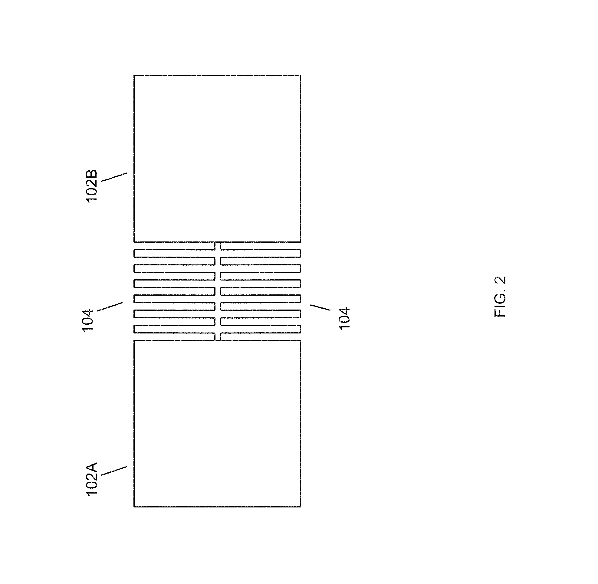
FIG. 3 depicts an overhead view of an embodiment of the present invention showing two device islands connected edge-to-edge by three extremely stretchable interconnects; in this case, the long bars of the interconnects are rotated by 90.degree. which allows them to be longer than if they were not rotated.
FIG. 4 depicts four device islands arranged in a square matrix in an embodiment of the present invention, with each edge connected by an extremely stretchable interconnect to its nearest neighbors island edge, and the interconnects are formed so as to maximize the amount of chip area that is used for either an island or interconnect.
FIG. 5 depicts the case of FIG. 1, with the short bars widened for extra mechanical strength at those locations.
FIGS. 6A and 6B depict embodiments of the present invention, where FIG. 6A is a side view of device islands and extremely stretchable interconnects transferred onto an elastomeric substrate. In this case, the substrate has been molded to have posts that are of the same area as the device islands (note that in embodiments these could be smaller or larger than the device islands). The height "h" of the molded post regions may range from, but is not limited to, about 1-1000 .mu.m. The interconnects are located in between these regions as shown. FIG. 6B is a side view as before, with a similarly shaped elastomeric superstrate to serve as an encapsulation layer protecting the devices from direct mechanical contact.
FIG. 7 depicts a side view of a two-layer PDMS substrate in an embodiment of the present invention comprising silicon device islands adhered to top layer, free-standing interconnects, and square wave ripples in the lower layer PDMS to promote increased stretching through the substrate.
FIG. 8 depicts an embodiment of the present invention with a side view of two layers of cured photoresist (SU-8 50 and SU-8 2002) used to make the two-layer PDMS substrate described in FIG. 7.
FIG. 9 depicts an embodiment of the present invention with a side view of a two-layer PDMS substrate consisting of sinusoidal waves in the lower layer of PDMS to promote increased stretching through the substrate.
While the invention has been described in connection with certain preferred embodiments, other embodiments would be understood by one of ordinary skill in the art and are encompassed herein.
All documents referenced herein are hereby incorporated by reference.
DETAILED DESCRIPTION OF THE INVENTION
The present invention accomplishes extremely stretchable electronics by forming the electronics on discrete islands 102 of silicon.
With reference to the present invention, the term "stretchable", and roots and derivations thereof, when used to modify circuitry or components thereof is meant to encompass circuitry that comprises components having soft or elastic properties capable of being made longer or wider without tearing or breaking, and it is also meant to encompass circuitry having components (whether or not the components themselves are individually stretchable as stated above) that are configured in such a way so as to accommodate and remain functional when applied to a stretchable, inflatable, or otherwise expandable surface. The term "expandable", and roots and derivations thereof, when used to modify circuitry or components thereof is also meant to have the meaning ascribed above. Thus, "stretch" and "expand", and all derivations thereof, may be used interchangeably when referring to the present invention.
In embodiments, the discrete islands mention above are discrete operative (in embodiments, arranged in a "device island" arrangement) and are themselves capable of performing the functionality described herein, or portions thereof. In embodiments, such functionality of the operative devices can include integrated circuits, physical sensors (e.g. temperature, pH, light, radiation etc), biological and/or chemical sensors, amplifiers, A/D and D/A converters, optical collectors, electromechanical transducers, piezo-electric actuators, light emitting electronics which include LEDs, and combinations thereof. The purpose and advantage of using standard ICs (in embodiments, CMOS, on single crystal silicon) is to have and use high quality, high performance, and high functioning circuit components that are also already commonly mass-produced with well known processes, and which provide a range of functionality and generation of data far superior to that produced by a passive means.
In an example, the discrete islands 102 may range from about, but not limited to, 10-100 .mu.m in size measured on an edge or by diameter, and connecting said islands 102A-B with one or more extremely stretchable interconnects 104. The novel geometry of the interconnects 104 is what makes them extremely compliant. Each interconnect 104 is patterned and etched so that its structural form has width and thickness dimensions that may be of comparable size (such as their ratio or inverse ratio not exceeding about a factor of 10); and may be preferably equal in size. In embodiments, the dimensions may not be greater than about Sum (e.g. where both dimensions are about 1 .mu.m or less). The interconnect 104 may be formed in a boustrophedonic style such that it effectively comprises long bars 108 and short bars 110 as shown in FIG. 1. This unique geometry minimizes the stresses that are produced in the interconnect 104 when subsequently stretched because it has the effective form of a wire, and behaves very differently than interconnect form factors having one dimension greatly exceeding the other two (for example plates). Plate type structures primarily relieve stress only about a single axis via buckling, and withstand only a slight amount of shear stress before cracking. This invention may relieve stress about all three axes, including shears and any other stress.
In addition, because the interconnect 104 may be formed out of rigid materials, after being stretched it may have a restorative force which helps prevent its wire-like form from getting tangled or knotted when re-compressing to the unstretched state. Another advantage of the boustrophedonic geometry is that it minimizes the initial separation distance between the islands 102A-B. This is illustrated in FIG. 1. One or more interconnects 104 may be formed in various ways, as shown in FIGS. 2-4. The parts of the interconnect 104 where the majority of stresses build up during stretching may be the short linking bars. To minimize cracking here, the short linking bars 110A may be made several micrometers wider than the longer bars 108, as shown in FIG. 5.
In embodiments, the connection point of the interconnect 104 to the device island 102 may be anywhere along the device island edge, or may be at a point on the surface of the device island 102 (in which case the interconnect may be located just above the plane of the device island).
In embodiments, device islands 102 may be made on any suitable material substrate, provided that a top membrane layer of said substrate that contains the ICs can be freed from the bulk of the substrate and transfer printed onto an elastomeric substrate.
In the present invention, the interconnects 104 (as described herein) may be formed either monolithically (i.e., out of the same semiconductor material as the device islands) or may be formed out of another material. In one non-limiting example embodiment, the stretchable electronics arc fabricated on a silicon-on-insulator (SOI) wafer, having a 1 .mu.m thick top silicon layer and a 1 .mu.m thick buried oxide layer. Devices arc formed on the top silicon wafer, and arranged into a square pattern of islands 102A-D and interconnects 104 of the general form shown in FIG. 4, in which the islands 102 are 100 .mu.m on an edge, and the interconnects 104 are 1 .mu.m wide, and the space between each long bar is 1 .mu.m, and the interconnects 104 comprise 10 long bars 108, all about 100 jam long. The islands 102 and interconnects 104 are formed in an etching step which removes the excess silicon. The islands 102 and interconnects 104 are coated with a 1 .mu.m layer of polyimide that is patterned to only cover the islands 102 and interconnects 104. Next, the islands 102 and interconnects 104 are released in an HF etch which undercuts the underlying buried oxide. After drying, the islands 102 and interconnects 104 are transfer printed with a Polydimethylsiloxane (PDMS) stamp onto an elastomeric substrate 602. After being picked up by the transfer stamp, and prior to being placed onto the elastomeric substrate 602, the backsides of the islands 102 may be coated with a layer of polyimide (patterned to only cover the islands 102 and interconnects 104), and an additional layer of evaporated 3 nm chromium and 30 nm silicon dioxide selectively over the island regions to improve adhesion to the elastomeric substrate 602 at those locations, and not along the interconnects 102. The elastomeric substrate 602 may be PDMS or another highly compliant material. The elastomeric substrate 602 may additionally be molded or etched into the shape shown in FIGS. 6A and 6B, to further increase selective adhesion in the device island region but not the interconnect region, and to reduce the amount of material strain in the elastomeric substrate 602 that is transferred to the device islands 102. In this example, the interconnects may accommodate stretching the device islands apart by approximately up to 800 .mu.m. In addition, the interconnects 104 of this example may be capable of accommodating lateral shear displacements of about 800 .mu.m. In general, they may be capable of accommodating any relative displacement of the two islands such that they remain approximately within 800 .mu.m of each other. In addition, the interconnects 104 may accommodate corkscrew type rotations of one island relative to another about any of the three axes of rotation. This feature may be limited only by the interconnects becoming entangled within each other. In any practical application, the completed stretchable device may not be so severely rotated, and the interconnect may easily accommodate rotations of up to 180.degree.. It is noted that by increasing the number of long bars 108 used in the interconnect 104, or by increasing the length of the long bars 108, the interconnect may be able to accommodate even larger displacement strains. In embodiments, there may be no practical upper limit to the amount of displacement enabled through the present invention.
In another embodiment the elastomeric substrate 602 may comprise two layers separated by a height. The top "contact" layer contacts the device island 102 as in the embodiment illustrated in FIG. 6. In addition, FIG. 7 shows the bottom layer 702 may be a "wavy" layer containing ripples or square waves molded into the substrate 602 during elastomer fabrication. These square waves enable additional stretching, whose extent depends on the amplitude and wavelength of the waves pattern-molded in the elastomer 602. FIG. 7 shows one non-limiting layout and topology of an elastomeric substrate 602 relative to the position of the interconnects 104 and device islands 102A-B. In an example, a two layer molded substrate can be fabricated using two step process consisting of two types of negative photoresist (SU-8 50 and SU-8 2002; Microchem Corporation). The negative resists can be spin-coated on a transfer silicon wafer with spin speeds of 3000 rpm. The SU-8 50 layer can be spun on the wafer, and subsequently cured with UV radiation. Once the SU-8 50 layer has hardened, the SU-8 2002 can be spun and cured with a photo-mask and an alignment tool. In this example, the thickness of the SU-8 50 and SU-8 2002 are 40-50 .mu.m 708 and 2-10 .mu.m 704, respectively. The 40-50 .mu.m thick regions of SU-8 50 contain ripples 702 of SU-8 2002 (in this instance in the form of square waves) on their surfaces. Upon curing of the SU-8 2002 layer, liquid PDMS can be poured over the SU-8 patterns to form a substrate in the shape of the SU-8 molds 802, as shown in FIG. 8. The amplitude of the ripples in the SU-8 mold 802 can be varied by changing the spin speed used for spinning the thin layer of SU-8 2002. In this configuration, the interconnects 104 are free-standing. The entire substrate-device configuration can be immersed in non-cured elastomer (fluid layer) layer followed by a cured layer of PDMS to encapsulate the fluid and devices.
In another embodiment, the PDMS in the lower layer may be designed with periodic sinusoidal ripples 702B. In embodiments, this ripple configuration may be achieved by bonding Si nanoribbons on the surface of pre-strained PDMS in a uniform parallel pattern. The release of the prestrain in the PDMS substrate generates sinusoidal waves along the thin Si-nanoribbons (caused by buckling) and the surface of the PDMS substrate. The amplitude and wavelength of these waves 702B may depend on the extent of uniaxial pre-strain exerted on the PDMS and on the mechanical properties of the Si-nanoribbons. The wavy surface on the PDMS may be used as a transfer mold. Two-part liquid plastic solution can be poured over the wavy PDMS substrate and cured at room temperature over time (.about.2 hrs). Once the plastic hardens, the plastic substrate can be peeled away from the PDMS. This new plastic transfer substrate with wavy surface features can be used to produce more PDMS substrates containing wave features. The wavy PDMS may serve as the lower layer of PDMS as in the previous embodiment. To produce a two layer PDMS structure, a top layer of PDMS can be plasma bonded to this lower layer of PDMS using oxygen plasma surface activation to produce the substrate illustrated in FIG. 9.
In another embodiment, the PDMS transfer stamp is stretched after the islands 102A-B and interconnects 104 are picked up. A subsequent transfer to another elastomeric substrate 602 may place these pre-stretched devices in a configuration, which allows the new elastomeric substrate to undergo compression. The devices may be able to accommodate that compression because the interconnects are pre-stretched.
In another embodiment, the interconnects 104 are not made out of the same material as the device islands 102. In this case, the islands 102A-B are completely isolated from each other by etching, with no interconnects in between. In an example, a layer of polyimide may then be deposited, contact vias etched to various locations on the surface of the device island 102, and then metal interconnects 104 deposited and patterned into a boustrophedonic pattern, followed by another layer of polyimide. Both layers of polyimide may now be patterned and etched to leave a small border around the interconnects 104 (thereby fully encapsulating the interconnects). These interconnects may have the advantage that they are already fully encapsulated in polyimide and will not adhere as well to the elastomeric substrate as the device islands will. The other advantage is that these interconnects may not be limited to only connecting along the edge of an island. The contact via may be etched anywhere on the surface of the island 102, including near the center. This may allow for easier connections to devices, more connections than possible only along an edge, increased strain compliance, decreased strain at the contact vias, and multiple layers of interconnects made with polymer passivation layers in between, allowing even more interconnects, or allowing one device island 102A to connect to a non-neighboring device island 102B.
In another embodiment of the invention, the device islands 102 are fabricated and transfer printed onto the elastomeric substrate 602, or substrate comprising a polymeric release layer and polymeric non-release layer. After transfer printing, the interconnects 104 are formed as described above, which may be possible because they do not require any high temperature processing, and then in the latter case, the release layer is etched and the devices that are on the non-release layer, are transfer printed onto another elastomeric substrate 602. In the former case, the islands 102 may be transferred onto the elastomeric substrate using pick and place technology so that islands 102 that are initially fabricated very close to each other are spread apart when they are transfer printed. This allows the interconnects 104 to be fabricated in a pattern that resembles their stretched configuration (if desired), to allow compression.
In embodiments, the present invention may comprise a stretchable electrical interconnect 104, including an electrical interconnect 104 for connecting two electrical contacts 102A-B (e.g. device islands 102A-B), where the electrical interconnect 104 may be arranged boustrophedonicially to define rungs 108 (i.e. long bars 108) between the contacts 102A-B, and where the rungs 108 may be substantially parallel with one another and where a plurality of rungs 108 may have substantially the same length and displacement therebetween. In addition, the ratio of the length of the plurality of rungs 108 and the displacement between the plurality of rungs 108 may be large, such as at least 10:1, 100:1, 1000:1, and the like. The electrical integrity of the electrical interconnect 104 may be maintained as stretched, such as to displacements that are increased to 1000%, 10000%, 100000%, and the like during stretching. In embodiments, the rungs 108 may be substantially perpendicular to the contacts 102A-B, the interconnection 104 may have a trace width and/or inter-rung spacing ranging between 0.1-10 microns. In embodiments, the two electrical contacts 102A-B may be located on an elastomeric substrate 602, the electrical contacts 102A-B may be bonded to the substrate 602 and the interconnection 104 not bonded to the substrate 602, the electrical contacts 102A-B may be semiconductor circuits, metal contacts, and the like.
In embodiments, the present invention may comprise a stretchable electrical interconnect 104, including an electrical interconnect 104 for connecting two electrical contacts 102A-B, where the electrical interconnect 104 is arranged boustrophedonicially to define rungs 108 between the contacts 102A-B, and where the interconnect 104 maintains electrical conductivity and electrical integrity when a displacement between the contacts 102A-B is increased, such as by 1000%, 10000%, 100000%, and the like.
In embodiments, the present invention may electrically interconnect two electrical contacts 102A-B with a stretchable interconnection 104 that has the ability to twist between the two electrical contacts 102A-B by up to approximately 180 degrees while maintaining electrical integrity of the stretchable interconnection 104.
In embodiments, the present invention may be a device including a body having a stretchable surface (e.g. an elastomeric substrate 602), and a stretchable electronic circuit including (i) a first discrete operative device 102A, (ii) a second discrete operative device 102B, and (iii) a stretchable interconnect 104 connecting the first discrete operative device 102A to the second discrete operative device 102B, where the interconnect 104 may have a substantially boustrophedonic pattern and be able to maintain electrical conductivity when stretched, such as up to 1000%, 10000%, 100000%, and the like. The stretchable electronic circuit may be affixed to the stretchable surface of the body. In embodiments, the connection may be to a metal contact, to a semiconductor device, and the like. The first discrete operative device 102A, the second discrete operative device 102B, and the stretchable interconnect 104 may all be made from the same material, and that material may be a semiconductor material.
In embodiments, the present invention may attach at least two isolated electronic components (which in embodiments may be discrete operative devices) 102A-B to an elastomeric substrate 602, and arrange an electrical interconnection 104 between the components 102A-B in a boustrophedonic pattern interconnecting the two isolated electronic components 102A-B with the electrical interconnection 104. The elastomeric substrate 602 may then be stretched such that components 102A-B separate relative to one another, where the electrical interconnection 104 maintains substantially identical electrical performance characteristics that the electrical interconnection 104 had in a pre-stretched form. In embodiments, the stretching may be a translational stretching, where the separation between the isolated electronic components 102A-B increases by a percent as a result of the stretching, such as 10%, 100%, 1000%, 10000%, 100000%, and the like. The stretching may be a rotational stretching, where the rotation may be greater than a certain rotation angle, such as 90.degree., 180.degree., 270.degree., 360.degree., and the like, where the stretching may be in all three axes. In embodiments, the electrical interconnection 104 may be made from semiconducitve material. The electrical interconnection 104 may be made from the same semiconductor material as the isolated electronic components 102A-B, fabricated at the same time as the isolated electronic components 102A-B, and the like. The semiconductor material may be a single crystal semiconductor material. The electrical interconnection 104 may made of a different material than the isolated electronic components 102A-B, such as a metal. In embodiments, the interconnect material 104 may be loosely bound to the elastomeric substrate 602, not connected at all, raised above the surface of the elastomeric substrate 602, and the like. In embodiments, the at least two isolated semiconductor circuits may be fabricated on an upper surface 604 of the elastomeric substrate 602 separated by a lower surface 608 of the elastomeric substrate 602, and the electrical interconnection 104 may be fabricated at the level of the upper surface 604 of the elastomeric substrate 602. In this way, the electrical interconnection 104 may have no direct contact with the lower level 608, and thereby be substantially free from adhesion to the lower level 608 during stretching. In addition, the lower surface 608 of the elastomeric substrate 602 may include a wavy form 702, where the wavy form 704 may allow the elastomeric substrate 602 to expand during stretching.
While the invention has been described in connection with certain preferred embodiments, other embodiments would be understood by one of ordinary skill in the art and are encompassed herein.
All documents referenced herein are hereby incorporated by reference.
* * * * *
References
D00000
D00001
D00002
D00003
D00004
D00005
D00006
D00007
D00008
XML
uspto.report is an independent third-party trademark research tool that is not affiliated, endorsed, or sponsored by the United States Patent and Trademark Office (USPTO) or any other governmental organization. The information provided by uspto.report is based on publicly available data at the time of writing and is intended for informational purposes only.
While we strive to provide accurate and up-to-date information, we do not guarantee the accuracy, completeness, reliability, or suitability of the information displayed on this site. The use of this site is at your own risk. Any reliance you place on such information is therefore strictly at your own risk.
All official trademark data, including owner information, should be verified by visiting the official USPTO website at www.uspto.gov. This site is not intended to replace professional legal advice and should not be used as a substitute for consulting with a legal professional who is knowledgeable about trademark law.