Nano metallic planar apex optical detector
Xin , et al. A
U.S. patent number 10,381,397 [Application Number 15/926,748] was granted by the patent office on 2019-08-13 for nano metallic planar apex optical detector. This patent grant is currently assigned to Black Sesame International Holding Limited. The grantee listed for this patent is Black Sesame Technologies Inc.. Invention is credited to Dong Wei, Zhaowei Xin.
| United States Patent | 10,381,397 |
| Xin , et al. | August 13, 2019 |
Nano metallic planar apex optical detector
Abstract
A nano-metallic-planar-apex optical detector, comprising a semiconductor optical detector and a nano array mask defining a plurality of polygonal apertures connected to the optical detector, wherein the semiconductor optical detector detects near-field light focused b the nano array.
| Inventors: | Xin; Zhaowei (Wuhan, CN), Wei; Dong (Wuhan, CN) | ||||||||||
|---|---|---|---|---|---|---|---|---|---|---|---|
| Applicant: |
|
||||||||||
| Assignee: | Black Sesame International Holding
Limited (Santa Clara, CA) |
||||||||||
| Family ID: | 66432463 | ||||||||||
| Appl. No.: | 15/926,748 | ||||||||||
| Filed: | March 20, 2018 |
Prior Publication Data
| Document Identifier | Publication Date | |
|---|---|---|
| US 20190148452 A1 | May 16, 2019 | |
Related U.S. Patent Documents
| Application Number | Filing Date | Patent Number | Issue Date | ||
|---|---|---|---|---|---|
| 62586011 | Nov 14, 2017 | ||||
| Current U.S. Class: | 1/1 |
| Current CPC Class: | H01L 31/0232 (20130101); H04N 5/33 (20130101); H01L 31/108 (20130101); H01L 27/14669 (20130101); H01L 33/58 (20130101); H01L 27/14627 (20130101); H01L 31/02327 (20130101) |
| Current International Class: | H01L 31/0232 (20140101); H04N 5/33 (20060101); H01L 27/146 (20060101); H01L 33/58 (20100101) |
| Field of Search: | ;257/432 |
References Cited [Referenced By]
U.S. Patent Documents
| 5973316 | October 1999 | Ebbesen |
| 6040936 | March 2000 | Kim |
| 6236033 | May 2001 | Ebbesen |
| 6441945 | August 2002 | Atwater |
| 8094394 | January 2012 | Yamada |
| 9368667 | June 2016 | Kim |
| 9464985 | October 2016 | Liu |
| 2006/0274315 | December 2006 | Saito |
| 2007/0096087 | May 2007 | Catrysse |
| 2009/0261250 | October 2009 | Zhou |
| 2009/0296246 | December 2009 | Yamada |
| 2013/0134309 | May 2013 | Rapaport |
| 2013/0181129 | July 2013 | Berte |
| 2013/0192226 | August 2013 | Stettenheim |
| 2014/0168651 | June 2014 | Guo |
| 2014/0191113 | July 2014 | Atwater |
| 2014/0291479 | October 2014 | Lu |
| 2015/0036234 | February 2015 | Ben-Yakar |
| 2015/0284852 | October 2015 | Pokroy |
| 2016/0343887 | November 2016 | Hossain |
| 2016/0357026 | December 2016 | Astratov |
| 2017/0102617 | April 2017 | Fischer |
| 2017/0201658 | July 2017 | Rosenblatt |
| 2017/0293053 | October 2017 | Cheatham, III |
| 2018/0106933 | April 2018 | Chanda |
Attorney, Agent or Firm: Wang; Timothy T. Ni, Wang & Massand, PLLC
Claims
What is claimed is:
1. A nano-metallic-planar-apex optical detector, comprising: a semiconductor optical detector; and a nano array mask defining a plurality of polygonal apertures connected to the optical detector, wherein the semiconductor optical detector detects near-field light focused by the nano array; and wherein the nano array mask comprises a cadmium adhesion layer and a gold layer.
2. Wherein the nano-metallic-planar-apex optical detector of claim 1 wherein the nano array mask defining at least one box aperture having at least one isosceles triangular insert remaining along at least one edge of an inside of the at least one box aperture.
3. Wherein the nano-metallic-planar-apex optical detector of claim 1 wherein the nano array mask defining at least one isotoxal square star aperture.
4. Wherein the nano-metallic-planar-apex optical detector of claim 1 wherein the nano array mask defining at least one box aperture having at least one rhombus insert remaining within the at least one box aperture.
5. Wherein the nano-metallic-planar-apex optical detector of claim 1 wherein the nano array mask defining at least one box aperture having a plurality of rhombus inserts remaining within the at least one box aperture.
6. Wherein the nano-metallic-planar-apex optical detector of claim 1 wherein the nano array mask defining at least one box aperture having at least one bow tie aperture along at least one inside edge of the at least one box aperture.
7. Wherein the nano-metallic-planar-apex optical detector of claim 1 wherein the nano array mask defining at least one box aperture having a plurality of bow tie apertures along at least one inside edge of the at least one box aperture.
8. Wherein the nano-metallic-planar-apex optical detector of claim wherein the nano array mask defining at least one box aperture haying a plurality of isosceles triangular inserts remaining along at least one inside edge of the at least one box aperture.
9. Wherein the nano-metallic-planar-apex optical detector of claim 1 wherein the nano array mask defining at least one box aperture having triangular metal remaining along at least one inside edge of the at least one box aperture.
10. A nano-metallic-planar-apex optical detector, comprising: a nano array mask defining a plurality of polygonal apertures that form a plurality of Schottky contact electrodes; a semiconductor optical detector, having a semiconductor optical detector first side connected to the plurality of Schottky contact electrodes wherein the semiconductor optical detector detects near-field light focused by the array, the semiconductor optical detector having a semiconductor optical detector second side opposite the semiconductor optical detector first side; and a plurality of ohmic contact electrodes aligned with the nano array and connected to the semiconductor optical detector second side.
11. Wherein the nano-metallic-planar-apex optical detector of claim 10 wherein the nano array mask defining at least one box aperture having at least one isosceles triangular insert remaining along at least one inside edge of the at least one box aperture.
12. Wherein the nano-metallic-planar-apex optical detector of claim 10 wherein the nano array mask defining at least one isotoxal square star aperture.
13. Wherein the nano-metallic-planar-apex optical detector of claim 10 wherein the nano array mask defining at least one box aperture having at least one rhombus insert remaining within the at least one box aperture.
14. Wherein the nano-metallic-planar-apex optical detector of claim 10 wherein the nano array mask defining at least one box aperture having a plurality of rhombus inserts remaining within the at least one box aperture.
15. Wherein the nano-metallic-planar-apex optical detector of claim 10 wherein the nano array mask defining at least one box aperture having at least one bow tie aperture along at least one of inside edge of the at least one box aperture.
16. Wherein the nano-metallic-planar-apex optical detector of claim 10 wherein the nano array mask defining at least one box aperture having a plurality of bow tie apertures along at least one inside edge of the at least one box aperture.
17. Wherein the nano-metallic-planar-apex optical detector of claim 10 wherein the nano array mask defining at least one box aperture having a plurality of isosceles triangular inserts remaining along at least inside edge of the at least one box aperture.
18. Wherein the nano-metallic-planar-apex optical detector of claim 10 wherein the nano array mask defining at least one box aperture having triangular metal remaining along at least one inside edge of the at least one box aperture.
19. Wherein the nano-metallic-planar-apex optical detector of claim 10 wherein the nano array mask comprises a cadmium adhesion layer and a gold layer.
Description
BACKGROUND
(1) Technical Field
The instant disclosure pertains to optical defectors, specifically nano-metallic-planar-apex metamaterial infrared detectors.
(2) Background
Currently silicon based infrared detectors are inefficient because the energy of the infrared incident photons is less than that which causes electron excitation from the valence to the conduction band. Currently detectors for the infrared region are built on substrates of Indium Gallium Arsenide (InGaAs) or Germanium (Ga), which have a lower energy bandgap. InGaAs and Ga infrared optical detectors may be difficult to fabricate and may be expensive.
Several approaches to detect infrared light in silicon have been demonstrated over the years, for example, solid-state thin film for infrared-to-visible up-conversion employing lead sulphide colloidal nanocrystals as a sensitizer, pyramidally shaped plasmonic concentrator Schottky detectors, and nonlinear processes such as two-photon absorption.
What is sought is a device capable of efficiently detecting photons in the optical and near-infrared spectral regions. A device utilizing nanoscale arrays may provide a solution to efficient detection of infrared photons utilizing a silicon substrate.
SUMMARY OF THE INVENTION
In one embodiment a nano-metallic-planar-apex optical detector, comprising a semiconductor optical detector and a nano array mask defining a plurality of polygonal apertures connected to the optical detector, wherein the semiconductor optical detector detects near-field light focused by the nano array.
In a further embodiment a nano-metallic-planar-apex optical detector, comprising a nano array mask defining a plurality of polygonal apertures that form a plurality of Schottky contact electrodes, a semiconductor optical detector, having a semiconductor optical detector first side connected to the plurality of Schottky contact electrodes wherein the semiconductor optical detector detects near-field light focused by the array, the semiconductor optical detector having a semiconductor optical detector second side opposite the semiconductor optical detector first side and a plurality of ohmic contact electrodes aligned with the nano array and connected to the semiconductor optical detector second side.
The details of one or more embodiments of the invention are set forth in the accompanying drawings and the description below. Other features, objects, and advantages of the invention will be apparent from the description and drawings, and from the claims.
DESCRIPTION OF THE DRAWINGS
FIG. 1 is the first illustrative drawing of nano-metallic-planar-apex arrays in accordance with at least one embodiment of the disclosure.
FIG. 2 is the second illustrative drawing of a nano-metallic-planar-apex array optical detector in accordance with one embodiment of the disclosure.
FIG. 3 is the third illustrative drawing of a nano-metallic-planar-apex array optical detector in accordance with one embodiment of the disclosure.
Like reference numbers and designations in the various drawings indicate like elements.
DETAILED DESCRIPTION OF THE INVENTION
The disclosure describes an optical concentrator is shown utilizing a nano-focusing effect of incident light based on surface plasmon polartons (SPPs) on nano-metallic-planar-apex metamaterials (NMPAM). The NMPAM may be used to enhance the strength of the surface evanescent and excitation of several SPP modes on the metal surface. The interaction of different SPPs result in unique near-field optical properties for imaging and optical storage, so as to focus light into a nano-size point and thus enhance the light power. The NMPAM may be utilized for coupling with infrared pixels to enhance the incident light converging so as to improve signal to noise ratio of infrared detection.
A new way to detect infrared light using a silicon substrate is shown by utilizing nano-metallic-planar-apex metamaterials (NMPAM). The NMPAM comprises a silicon substrate and a gold film with nano-planar-apex apertures. The silicon substrate shares a common interface with the gold and a Schottky barrier is created. The energy barrier height is thus lowered to a point lower than the energy barrier height of silicon, and lower than infrared photons.
Illuminated by infrared light, electrons on the old film may cross over the Schottky barrier into silicon. When under a reverse bias, they are collected as a photocurrent. The NMPAM is used to focus the incident light into .about.100 nm-scale and consequently enhance the electric power and improve the signal to noise ratio.
The concentration of the optical energy into nanoscale structures and enhancement of optical fields within nanoscale spatial regions is achieved using a lightning-rod effect. The lightning-rod effect is a broadband phenomenon that involves the enhancement of a local near field as a consequence of the high local charge densities present near the sharp metal tip. The non-resonant interaction of incident light with metallic nanostructures leads to enhancement of the near field on the planar apex, which may be detected by the common silicon photodetectors.
The gold planar apexes perform efficiently as broadband light concentrators, collecting light from a large area into a small active pixel area, thus providing high responsivity with low dark current.
In one example a detector was fabricated on a single side polished 2-inch p-type 350 .mu.m thick silicon wafer with {111} crystallographic plane orientation. A five (5) nano-meter layer of Cadmium (Ca) was deposited as an adhesion layer on the silicon substrate and a one hundred (100) nanometer gold layer was then sputtered on the Cadmium. Mask patterns were defined by Focused Ion Beam (FIB).
With respect to the polarization of incoming light, it was found that when the polarization is parallel to an apex direction of the mask that the light is concentrated to the tip of the mask aperture. When the polarization is perpendicular to the apex direction of the mask aperture, the light concentrated to the basic angles of the aperture and concentrated to the tip. Thus it was found that the NMPAM structure results in polarization independence.
It was found that when the NMPAM sample illuminated by light, the interaction of light and the mask gives rise to the collective oscillation of free-electrons on the metal surface. The free-electrons oscillated along the direction of the electromagnetic radiation and that the oscillation direction is parallel with the polarization.
As the oscillation wave spreads to the tip of the mask aperture, the oscillation of the free electron at the apex may be enhanced. For the light-bar effect, the concentration of the free-electron is strong, because the oscillation at the apex is enhanced; the intensity of near-field light may be enhanced. As the result of the lightning-rod effect, the density of the electrical field at the apex is high. As the same time, the large charge density and the oscillation enhance the apex near-field light.
Random polarization vectors of light may be resolved into x-component and y-components. The x-polarization light may give rise to the oscillation of free-electrons at transverse double-apex surfaces, the y-polarization light may result in oscillation of free-electrons at longitudinal double-apex surfaces. So, the NMPAM may be polarization independent, and function independently of the polarization of incoming light.
In the instant disclosure a simple design of a nano-focusing plasmonic metamaterials exhibiting spectrally near-field converge effect is described. The NMPAM may be applied to infrared detectors to improve the signal to noise ratio.
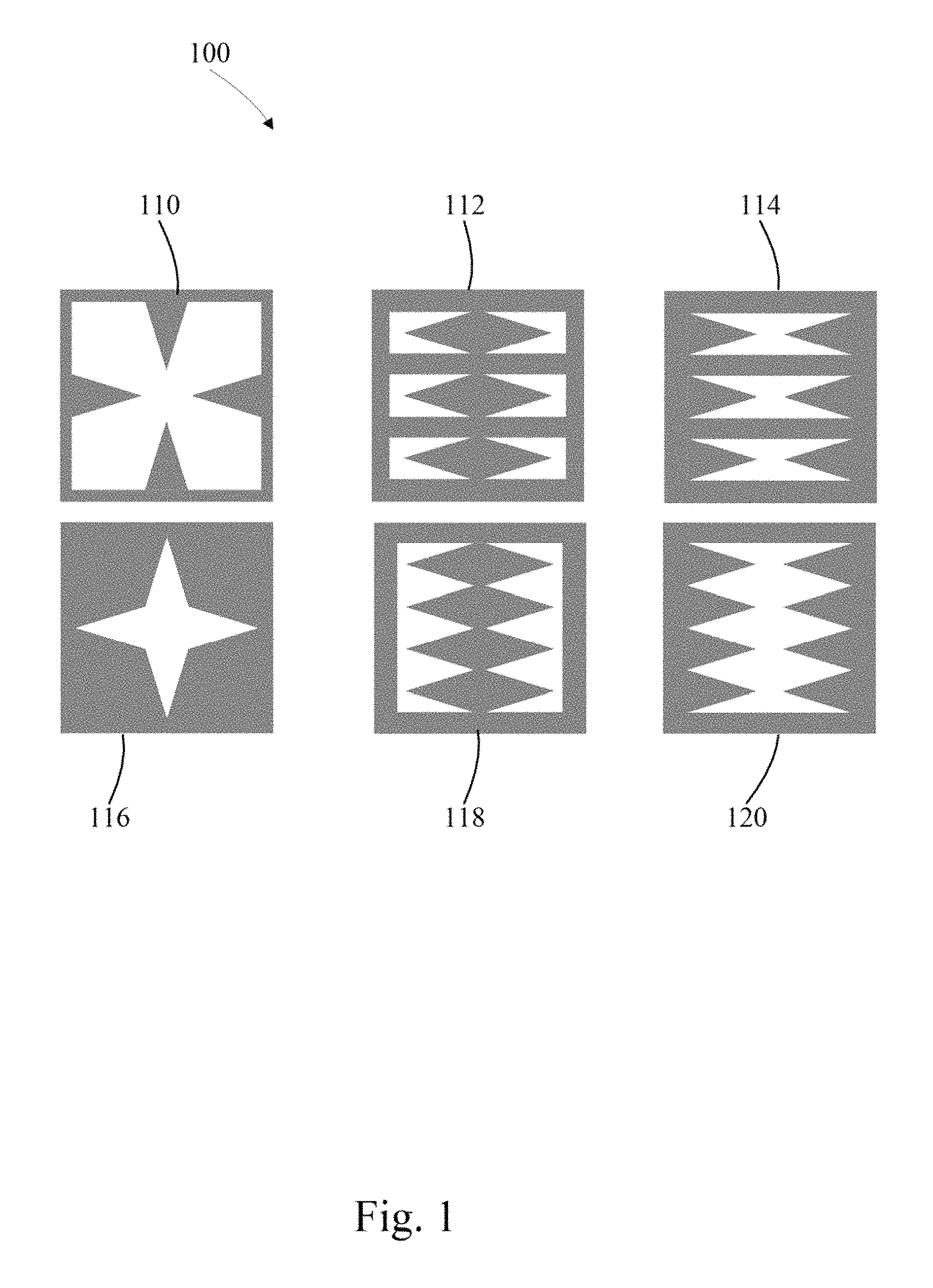
FIG. 1 shows an example design of nano-metallic-planar-apex arrays for nanofocusing of light and electron convergence. Element 110 has the nano array mask defining a box aperture having four isosceles triangular inserts along the inside edges of the box. Element 112 has the nano array mask defining three box apertures having a rhombus insert in each box. Element 114 shows the nano array mask defining three box apertures bow tie apertures within the boxes and multiple bow tie apertures the inside edges of the box. Element 116, shows the nano array mask defining at least one isotoxal square star aperture. Element 118 shows the nano array mask defining a box aperture having multiple rhombus inserts within the box. Element 120 shows the nano array mask defining a box aperture having multiple isosceles triangular inserts remaining along two inside edges of the box and triangular metal remaining along two inside edges of the box.
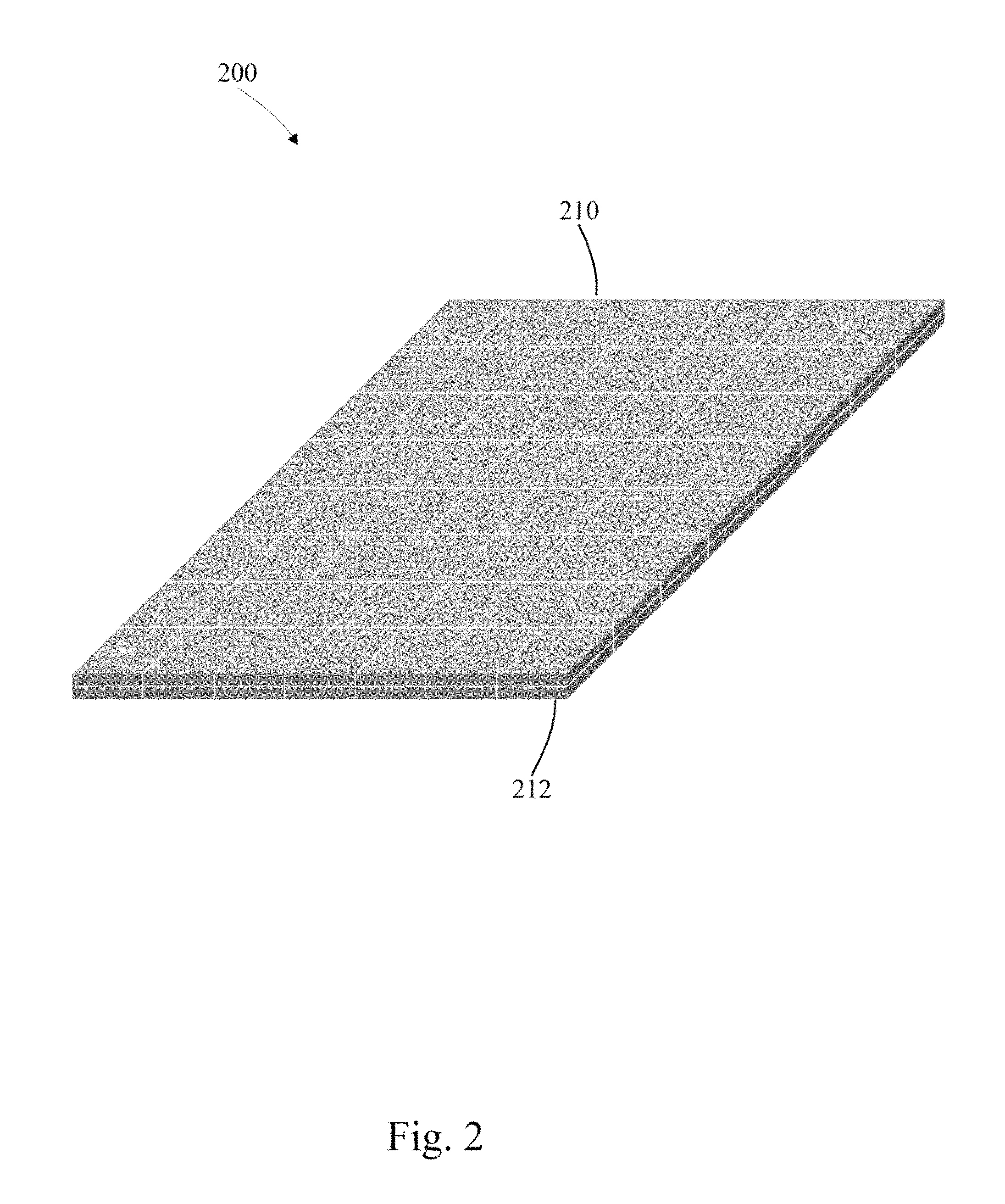
FIG. 2 illustrates an example design of a first detector. The nano-metallic-planar-apex arrays 210 are affixed directly to a detector 212. The detector detects near-field light which is nano focused by the nano-metallic-planar-apex arrays.
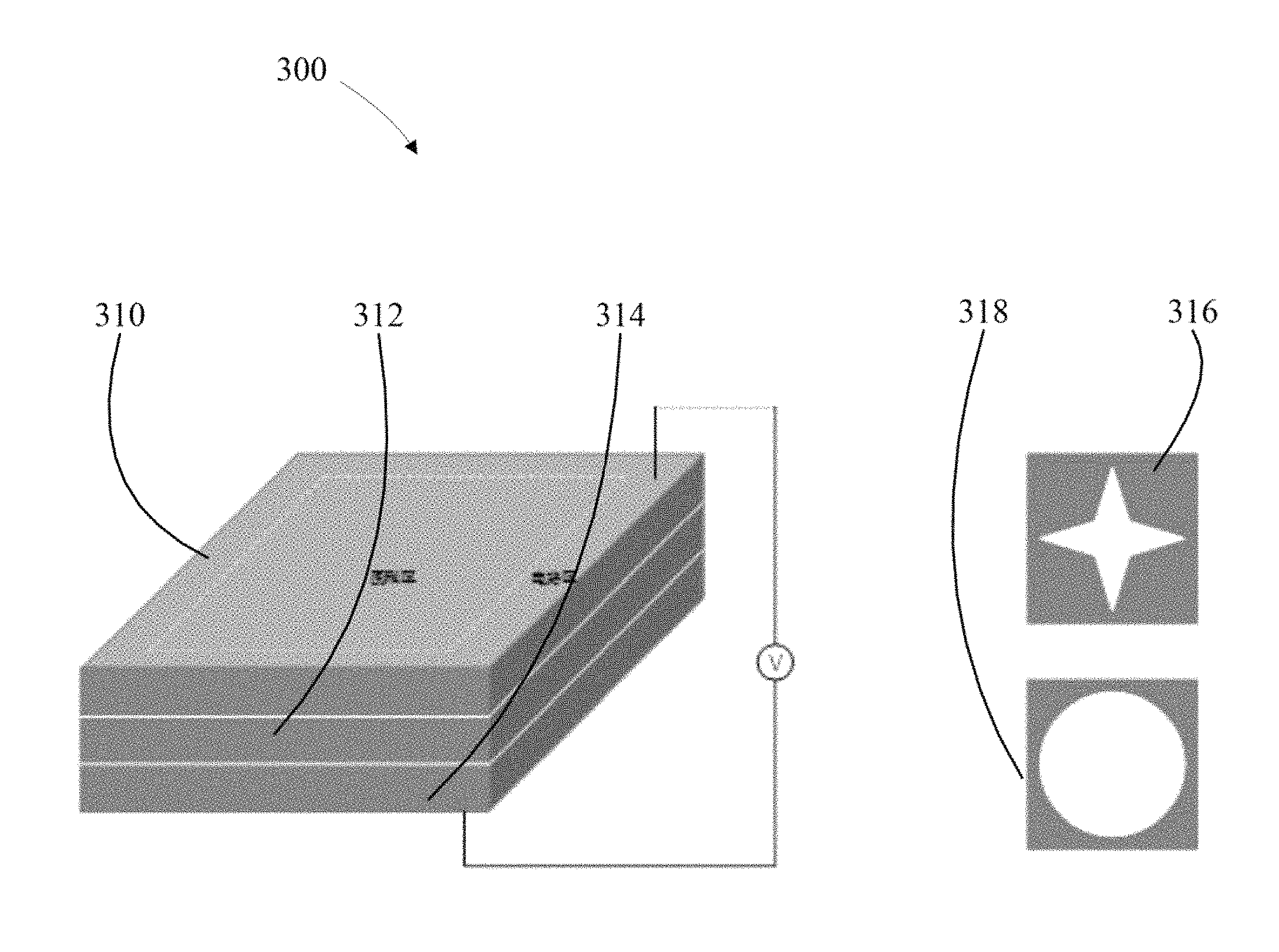
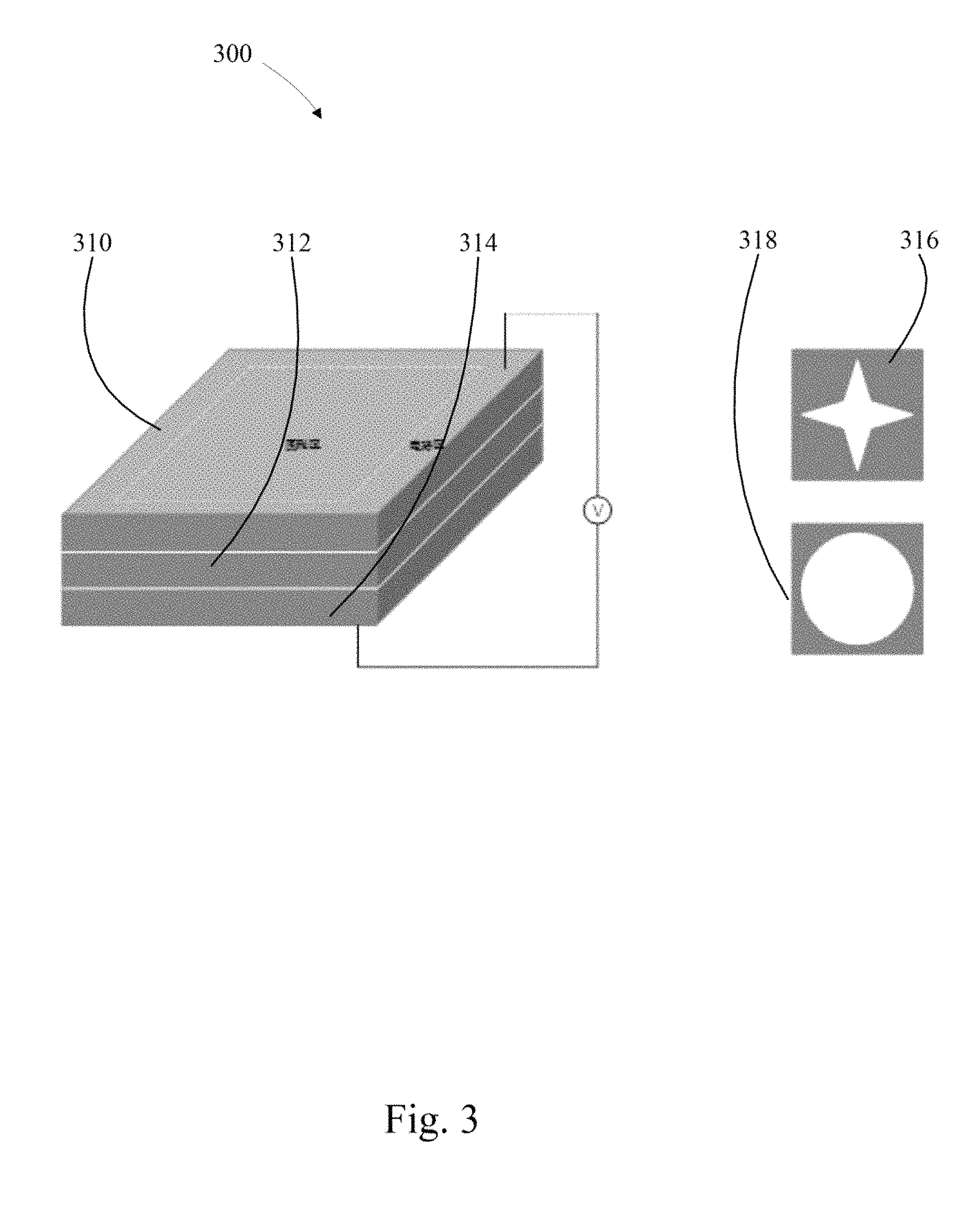
FIG. 3 illustrates an example design of a second detector. The top layer is a Schottky contact electrode 310, which is the metallic film with nano-planar-apex structure 316 in FIG. 1, the middle layer is a semiconductor 312 that acts as an optical detector and the bottom layer 314 is an ohmic contact electrode 318. There is a hole in the middle that allows incident light shines directly on the semiconductor. Different incidental lights will produce different photocurrents when voltage is applied. The Schottky contact electrodes are used to concentrate electrons and improve the signal-to-noise ratio.
It is to be understood that various modifications may be made without departing from the spirit and scope of the invention. It is to be understood that the foregoing description is intended to illustrate and not to limit the scope of the invention, which is defined by the scope of the following claims, and that other embodiments are within the scope of the claims.
* * * * *
D00000
D00001
D00002
D00003
XML
uspto.report is an independent third-party trademark research tool that is not affiliated, endorsed, or sponsored by the United States Patent and Trademark Office (USPTO) or any other governmental organization. The information provided by uspto.report is based on publicly available data at the time of writing and is intended for informational purposes only.
While we strive to provide accurate and up-to-date information, we do not guarantee the accuracy, completeness, reliability, or suitability of the information displayed on this site. The use of this site is at your own risk. Any reliance you place on such information is therefore strictly at your own risk.
All official trademark data, including owner information, should be verified by visiting the official USPTO website at www.uspto.gov. This site is not intended to replace professional legal advice and should not be used as a substitute for consulting with a legal professional who is knowledgeable about trademark law.