Optical processing head, optical processing apparatus, and control method and control program of optical processing apparatus
Ohno , et al.
U.S. patent number 10,371,645 [Application Number 14/888,281] was granted by the patent office on 2019-08-06 for optical processing head, optical processing apparatus, and control method and control program of optical processing apparatus. This patent grant is currently assigned to TECHNOLOGY RESEARCH ASSOCIATION FOR FUTURE ADDITIVE MANUFACTURING. The grantee listed for this patent is TECHNOLOGY RESEARCH ASSOCIATION FOR FUTURE ADDITIVE MANUFACTURING. Invention is credited to Kazuyuki Masukawa, Takashi Obara, Hiroshi Ohno, Mitsuo Sasaki, Yuji Sasaki.


| United States Patent | 10,371,645 |
| Ohno , et al. | August 6, 2019 |
Optical processing head, optical processing apparatus, and control method and control program of optical processing apparatus
Abstract
An optical processing head that detects a trouble of an optical processing head that will be generated at the time of optical processing before the trouble occurs is disclosed. The optical processing head that performs processing by condensing, on a process surface, a ray emitted by a light source for processing includes a cylindrical housing that surrounds a ray for processing emitted by the light source for processing, a ray emitter for inspection that is incorporated in the cylindrical housing and arranged outside the path of the ray for processing, and a light receiver that is incorporated in the cylindrical housing, arranged outside the path of the ray for processing, and receives a ray for inspection emitted by the ray emitter for inspection. The contamination of the inner surface of the cylindrical housing or the concentration of a scattering object flowing into the cylindrical housing is inspected by using a signal acquired from the light receiver.
| Inventors: | Ohno; Hiroshi (Yokohama, JP), Sasaki; Yuji (Yokohama, JP), Sasaki; Mitsuo (Yokohama, JP), Obara; Takashi (Yokohama, JP), Masukawa; Kazuyuki (Yokohama, JP) | ||||||||||
|---|---|---|---|---|---|---|---|---|---|---|---|
| Applicant: |
|
||||||||||
| Assignee: | TECHNOLOGY RESEARCH ASSOCIATION FOR
FUTURE ADDITIVE MANUFACTURING (Tokyo, JP) |
||||||||||
| Family ID: | 56878653 | ||||||||||
| Appl. No.: | 14/888,281 | ||||||||||
| Filed: | March 10, 2015 | ||||||||||
| PCT Filed: | March 10, 2015 | ||||||||||
| PCT No.: | PCT/JP2015/057074 | ||||||||||
| 371(c)(1),(2),(4) Date: | October 30, 2015 | ||||||||||
| PCT Pub. No.: | WO2016/143083 | ||||||||||
| PCT Pub. Date: | September 15, 2016 |
Prior Publication Data
| Document Identifier | Publication Date | |
|---|---|---|
| US 20170045462 A1 | Feb 16, 2017 | |
| Current U.S. Class: | 1/1 |
| Current CPC Class: | B23K 26/0643 (20130101); G01N 21/94 (20130101); G02B 5/08 (20130101); G02B 19/0076 (20130101); B23K 26/707 (20151001); G02B 27/0006 (20130101); B23K 26/0648 (20130101); G01N 21/15 (20130101); B23K 26/1476 (20130101); B23K 26/21 (20151001); G02B 19/0052 (20130101); B23K 26/03 (20130101); G01N 21/718 (20130101); G01N 2021/1757 (20130101); G01N 21/954 (20130101) |
| Current International Class: | G01N 21/94 (20060101); B23K 26/03 (20060101); B23K 26/06 (20140101); B23K 26/70 (20140101); G01N 21/15 (20060101); B23K 26/14 (20140101); G02B 27/00 (20060101); G02B 19/00 (20060101); B23K 26/21 (20140101); G02B 5/08 (20060101); G01N 21/954 (20060101); G01N 21/71 (20060101); G01N 21/17 (20060101) |
| Field of Search: | ;134/56R,1.1 ;356/342,239.2,237.2,336,301,337,445,124,318,73,28,237.1,369,237.3,341,442 ;250/574,573 ;219/121.63,121.6,121.67,121.83,121.75 |
References Cited [Referenced By]
U.S. Patent Documents
| 3705771 | December 1972 | Friedman |
| 3988068 | October 1976 | Sprague |
| 5198369 | March 1993 | Itoh |
| 5432601 | July 1995 | Tanaka |
| 5486676 | January 1996 | Aleshin |
| 5662822 | September 1997 | Tada et al. |
| 5793478 | August 1998 | Rader |
| 5835220 | November 1998 | Kazama |
| 5977515 | November 1999 | Uraki et al. |
| 6097025 | August 2000 | Modlin |
| 6271916 | August 2001 | Marxer |
| 6522386 | February 2003 | Nishi |
| 6778271 | August 2004 | Watson |
| 6778272 | August 2004 | Nakano |
| 6791057 | September 2004 | Kratzsch |
| 7084970 | August 2006 | Weiss |
| 7151603 | December 2006 | Kellie |
| 7206066 | April 2007 | Vurens |
| 7428041 | September 2008 | Kallio |
| 7656526 | February 2010 | Spuler |
| 7705292 | April 2010 | Hammann |
| 7821636 | October 2010 | Jeys |
| 7920261 | April 2011 | Jeys |
| 8319965 | November 2012 | Jeys |
| 8334972 | December 2012 | Thien |
| 8890023 | November 2014 | Dorsch |
| 2004/0032649 | February 2004 | Kondo |
| 2004/0156052 | August 2004 | Yamamoto |
| 2006/0192968 | August 2006 | Farrant |
| 2007/0146705 | June 2007 | Kaufmann |
| 2008/0117419 | May 2008 | Hays |
| 2008/0266666 | October 2008 | Hughes |
| 2010/0247934 | September 2010 | Meyer et al. |
| 2012/0080611 | April 2012 | Jones |
| 2014/0152986 | June 2014 | Trainer |
| 2014/0346155 | November 2014 | Jurca |
| 10 2008 015 133 | Sep 2009 | DE | |||
| 102008015133 | Sep 2009 | DE | |||
| 61-49689 | Apr 1986 | JP | |||
| 1-99792 | Apr 1989 | JP | |||
| 6-246466 | Sep 1994 | JP | |||
| 2003-117674 | Apr 2003 | JP | |||
| 2005-81399 | Mar 2005 | JP | |||
| 2005081399 | Mar 2005 | JP | |||
| 2014-237150 | Dec 2014 | JP | |||
| 2004/068069 | Aug 2004 | WO | |||
Other References
|
Pittl et al., "Apparatus for collecting process light during laser machining", Sep. 2009, DE-102008015133, Machine Translation (Year: 2009). cited by examiner . Shioji et al., "Method and apparatus for preventing contamination inside optical axis in laser machining apparatus", Mar. 2005, JP-2005081399, Machine Translation (Year: 2005). cited by examiner . Extended European Search Report (ESR) for corresponding European Application No. 15 78 5041.3. cited by applicant . Espacenet English abstract of DE 10 2008 015 133 A1. cited by applicant . International Search Report (ISR) dated Jun. 17, 2015 for International Application No. PCT/JP2015/057074. cited by applicant . J-PlatPat English abstract of JP 1-99792 A. cited by applicant . J-PlatPat English abstract of JP 2005-81399 A. cited by applicant . J-PlatPat English abstract of JP 6-246466 A. cited by applicant . Japanese Office Action dated Aug. 25, 2016 for Japanese Application No. 2015-549109 with English translation. cited by applicant . J-PlatPat English abstract of JP 2003-117674 A. cited by applicant . J-PlatPat English abstract of JP 2014-237150 A. cited by applicant. |
Primary Examiner: Barr; Michael E
Assistant Examiner: Bucci; Thomas
Attorney, Agent or Firm: Ladas & Parry LLP
Claims
The invention claimed is:
1. An optical processing head that performs processing by condensing, on a process surface, a ray emitted by a light source for processing, comprising: a cylindrical housing that surrounds a ray for processing emitted by the light source for processing; a condenser lens that condenses the ray for processing to a downstream side of the cylindrical housing toward the process surface; a ray emitter for inspection that is incorporated in said cylindrical housing, said ray emitter being arranged downstream of said condenser lens and arranged outside a path of the ray for processing; a light receiver that is incorporated in said cylindrical housing, said light receiver being arranged downstream of said condenser lens, being arranged outside the path of the ray for processing, and being arranged for receiving a ray for inspection emitted by said ray emitter for inspection, a mirror for observation that is disposed upstream of said condenser lens; and an image sensor that senses an image of the process surface using reflection from said mirror for observation, wherein one of a contamination of an inner surface of said cylindrical housing and a concentration of a scattering object flowing into said cylindrical housing is inspected by using a signal acquired from said light receiver, and wherein said light receiver is disposed on the downstream side of the ray emitter for inspection toward the process surface.
2. The optical processing head according to claim 1, wherein at least part of the inner surface of said cylindrical housing is a curved surface so as to reflect the ray for inspection by the inner surface of said cylindrical housing and condense the ray for inspection to said light receiver.
3. The optical processing head according to claim 2, wherein at least one of sections of the curved surface passing through both said ray emitter for inspection and said light receiver is an ellipse.
4. The optical processing head according to claim 3, wherein said ray emitter for inspection and said light receiver are arranged at two focus positions of the ellipse, respectively.
5. The optical processing head according to claim 4, wherein the curved surface has a shape conforming to an outer surface of a rotational ellipsoid, and said ray emitter for inspection and said light receiver are arranged at two focus positions, respectively, of the rotational ellipsoid.
6. The optical processing head according to claim 2, wherein the curved surface has a columnar shape having a diameter D using an optical axis of the ray for processing as a center, and letting .theta. be an angle defined by the optical axis and a line segment connecting said ray emitter for inspection and said light receiver, and L be a distance between said ray emitter for inspection and said light receiver, the following equation is established: D/L=2/tan .theta..
7. The optical processing head according to claim 1, wherein a concentration of a scattering object flowing into said cylindrical housing is inspected based on a temporal change of a signal acquired from said light receiver.
8. The optical processing head according to claim 1, wherein a contamination of the inner surface of said cylindrical housing is inspected based on a change, from a reference value, of a signal acquired from said light receiver.
9. An optical processing apparatus comprising: an optical processing head defined in claim 1; and a purge controller that changes, based on the signal, an amount of a purge gas ejected to the process surface.
10. A method of controlling an optical processing apparatus comprising an optical processing head according to claim 1, wherein the processing apparatus performs processing by condensing, on a process surface, a ray emitted by a light source for processing, the method comprising: changing, based on a signal acquired from said light receiver, an amount of a purge gas ejected to the process surface.
Description
RELATED APPLICATION
This application is an application under 35 U.S.C. 371 of International Application No. PCT/JP2015/057074 filed on Mar. 10, 2015, the entire contents of which are incorporated herein by reference.
TECHNICAL FIELD
The present invention relates to an optical processing head, an optical processing apparatus, and a control method and control program of the optical processing apparatus.
BACKGROUND ART
In the above technical field, patent literature 1 discloses a method using the ultrasonic vibration in order to detect contamination of a lens by a fine particle (fume or sputter) generated at the time of processing.
CITATION LIST
Patent Literature
Patent literature 1: U.S. Pat. No. 7,705,292
SUMMARY OF THE INVENTION
Technical Problem
In the technique described in this literature, however, the lens slightly vibrates at the time of ultrasonic vibration. Along with this, a condensed spot also oscillates, decreasing the processing accuracy.
The present invention enables to provide a technique of solving the above-described problem.
Solution to Problem
One aspect of the present invention provides an optical processing head that performs processing by condensing, on a process surface, a ray emitted by a light source for processing, comprising:
a cylindrical housing that surrounds a ray for processing emitted by the light source for processing;
a ray emitter for inspection that is incorporated in the cylindrical housing and arranged outside a path of the ray for processing; and
a light receiver that is incorporated in the cylindrical housing, arranged outside the path of the ray for processing, and receives a ray for inspection emitted by the ray emitter for inspection,
wherein one of a contamination of an inner surface of the cylindrical housing and a concentration of a scattering object flowing into the cylindrical housing is inspected by using a signal acquired from the light receiver.
Another aspect of the present invention provides a method of controlling an optical processing apparatus that performs processing by condensing, on a process surface, a ray emitted by a light source for processing, the optical processing apparatus including:
a cylindrical housing that surrounds a ray for processing emitted by the light source for processing;
a ray emitter for inspection that is incorporated in the cylindrical housing and arranged outside a path of the ray for processing; and
a light receiver that is incorporated in the cylindrical housing, arranged outside the path of the ray for processing, and receives a ray for inspection emitted by the ray emitter for inspection, the method comprising:
changing, based on the signal, an amount of a purge gas ejected to the process surface.
Still other aspect of the present invention provides a program of controlling an optical processing apparatus that performs processing by condensing, on a process surface, a ray emitted by a light source for processing, the optical processing apparatus including:
a cylindrical housing that surrounds a ray for processing emitted by the light source for processing;
a ray emitter for inspection that is incorporated in the cylindrical housing and arranged outside a path of the ray for processing; and
a light receiver that is incorporated in the cylindrical housing, arranged outside the path of the ray for processing, and receives a ray for inspection emitted by the ray emitter for inspection, the program causing a computer to execute:
changing, based on the signal, an amount of a purge gas ejected to the process surface.
Advantageous Effects of Invention
The present invention can provide an optical processing technique capable of detecting a trouble of an optical processing head that will be generated at the time of optical processing, before the trouble occurs.
BRIEF DESCRIPTION OF DRAWINGS
FIG. 1 is a view showing the arrangement of an optical processing head according to the first embodiment of the present invention;
FIG. 2 is a perspective view showing the arrangement of an optical processing head according to the second embodiment of the present invention;
FIG. 3 is a sectional view showing the arrangement of the optical processing head according to the second embodiment of the present invention;
FIG. 4 is a sectional view showing the arrangement of a ray emitter for inspection and a light receiver, and a ray path between them according to the second embodiment of the present invention;
FIG. 5 is a graph showing the arrangement relation between the ray emitter for inspection and the light receiver according to the second embodiment of the present invention;
FIG. 6 is a perspective view showing the arrangement of an optical processing head according to the third embodiment of the present invention;
FIG. 7 is a sectional view showing the arrangement of the optical processing head according to the third embodiment of the present invention;
FIG. 8 is a sectional view showing the arrangement of a ray emitter for inspection and a light receiver, and a ray path between them according to the third embodiment of the present invention;
FIG. 9 is a view showing the arrangement of an optical processing apparatus according to the fourth embodiment of the present invention; and
FIG. 10 is a flowchart showing the sequence of control by the optical processing apparatus according to the fourth embodiment of the present invention.
DESCRIPTION OF THE EMBODIMENTS
A preferred embodiment(s) of the present invention will now be described in detail with reference to the drawings. It should be noted that the relative arrangement of the components, the numerical expressions and numerical values set forth in these embodiments do not limit the scope of the present invention unless it is specifically stated otherwise. In the following embodiments, "light" includes various electromagnetic waves ranging from ultraviolet light to a microwave, and can be properly selected in accordance with a processing target or the like.
First Embodiment
An optical processing head 100 according to the first embodiment of the present invention will be described with reference to FIG. 1. FIG. 1 is a sectional view showing the optical processing head 100. The optical processing head 100 performs processing by condensing, on a process surface 140, a ray 110 emitted by a light source for processing (not shown).
The optical processing head 100 includes a cylindrical housing 101, a ray emitter 102 for inspection, and a light receiver 103.
The cylindrical housing 101 surrounds the ray 110 for processing emitted by the light source for processing. The ray emitter 102 for inspection is incorporated in the cylindrical housing 101 and arranged outside the path of the ray 110 for processing. The light receiver 103 is incorporated in the cylindrical housing 101, arranged outside the path of the ray 110 for processing, and receives a ray 121 for inspection emitted by the ray emitter 102 for inspection.
A contamination 111 of the inner surface of the cylindrical housing 101 or the concentration of a scattering object 112 flowing into the cylindrical housing 101 is inspected by using a signal 104 acquired from the light receiver 103. When the scattering object 112 flows into the cylindrical housing 101, it absorbs or scatters the ray 121 for inspection. As a result, the strength of the signal 104 decreases. That is, when the scattering object 112 is mixed, the signal 104 temporally changes, and the presence/absence of inflow of the scattering object 112 can be determined. When the contamination 111 is attached to the inner surface of the cylindrical housing 101, it absorbs the ray 121 for inspection, and the signal 104 becomes lower than a predetermined reference value. That is, the degree of contamination of the inner surface can be determined from a change of the signal 104 from a reference value.
The first embodiment can provide an optical processing technique in which, by detecting the contamination 111 on the inner surface of the cylindrical housing 101 or the concentration of the scattering object 112 flowing into the cylindrical housing 101, a trouble of the optical processing head that will be generated at the time of optical processing can be detected before the trouble occurs. In the present invention, the cylindrical housing 101 is not limited to a circular cylindrical shape, but suffices to have a cylindrical shape such as a square cylindrical shape, or another shape. The ray emitter 102 for inspection is not limited to a light source and may be the exit port of a light transmitting portion such as an optical fiber.
Second Embodiment
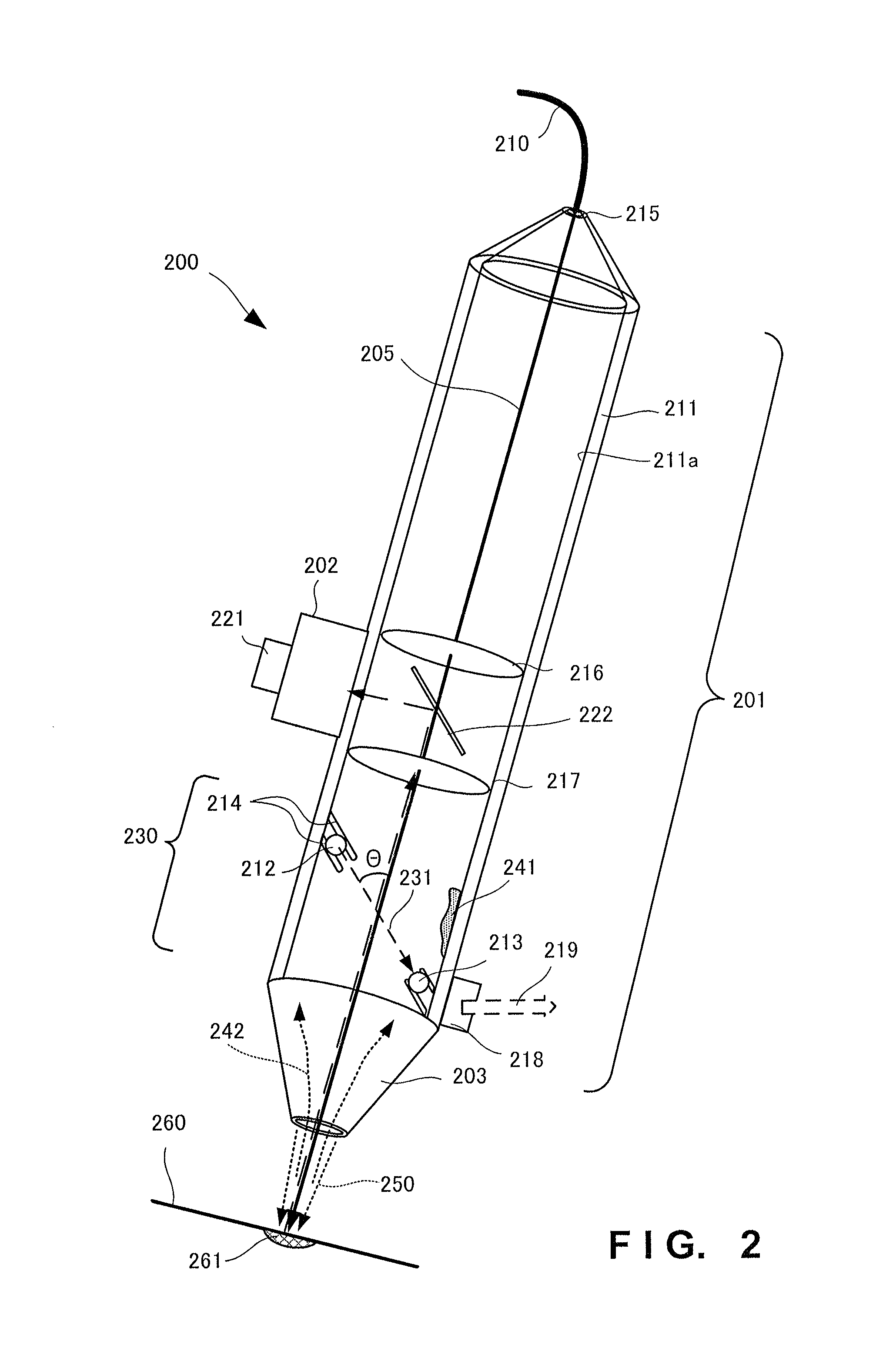
An optical processing head 200 according to the second embodiment of the present invention will be described with reference to FIG. 2. FIG. 2 is a view showing the internal arrangement of the optical processing head 200 to which a laser beam is applied. As shown in FIG. 2, the optical processing head 200 includes a condensing optical system device 201, an observation device 202, and a nozzle 203.
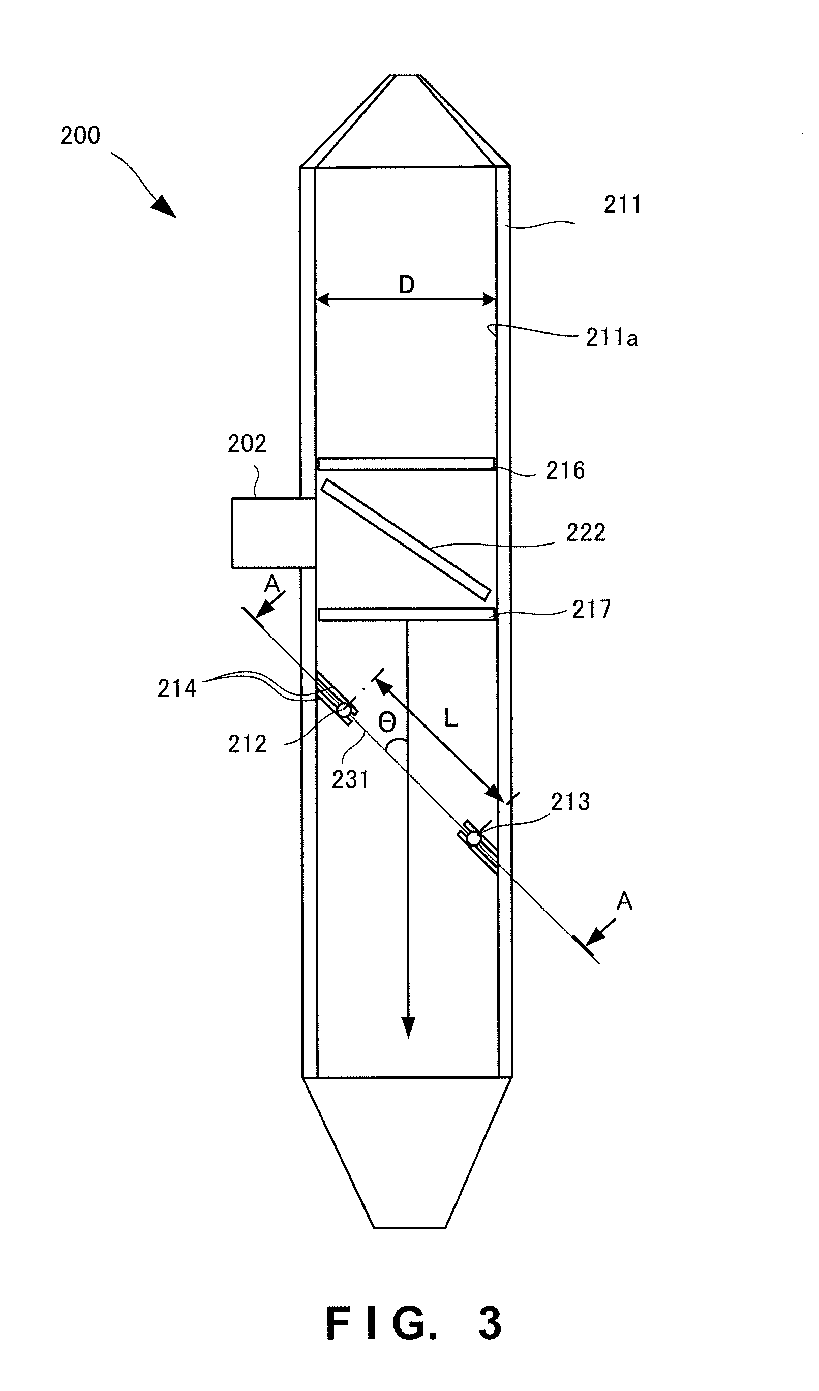
(Overall Arrangement of Head)
The condensing optical system device 201 is constituted by a collimator lens 216, a condenser lens 217, and a circular cylindrical housing 211 that holds them. The collimator lens 216 converts, into parallel light, a ray 205 for processing that travels from an incident end 215. The condenser lens 217 condenses the parallel light on a process surface 260 on the downstream side.
With these optical systems, the condensing optical system device 201 ejects, to the process surface 260, the ray 205 for processing that has been emitted by a light source (not shown), has passed through a light transmitting portion 210, and has been guided from the incident end 215. The light transmitting portion 210 is, for example, an optical fiber having a core diameter of .PHI.0.01 to 1 mm, and guides light (for example, a laser beam) generated by the light source to the optical processing head 200.
The ray 205 for processing that has been guided from the incident end 215 to the optical processing head 200 comes out to the process surface 260, and forms a molten pool 261 on the process surface 260.
The nozzle 203 receives supply of a processing material and gas from a material supply device (not shown) through a material supply portion, and ejects a material 250 mixed in the gas to the molten pool 261 of the process surface 260. After that, the molten pool 261 is cooled and hardened to deposit the material on the process surface 260. The molten pool 261 is moved on the process surface 260, and melting, material supply, and cooling are repeated, implementing three-dimensional shaping.
The observation device 202 is a device for observing the status of processing by the condensing optical system device 201 from a viewpoint along the optical axis of the ray 205 for processing. The observation device 202 includes an image capturing device 221 including an image sensor such as a CCD or CMOS sensor, and a one-way mirror 222 that is provided inside the condensing optical system device 201 and serves as a mirror for observation. The surface of the one-way mirror 222 is coated so that the one-way mirror 222 transmits the ray 205 for processing (wavelength: 1,060 nm), but reflects visible light (wavelength: 450 to 800 nm). Part of visible light reflected by the process surface 260 is reflected by the one-way mirror 222 and guided to the image capturing device 221. By performing feedback control of processing parameters in accordance with the observed processing status, the processing accuracy can be improved.
A ray emitter 212 for inspection and a light receiver 213 are arranged downstream of the condenser lens 217. The ray emitter 212 for inspection is arranged upstream of the ray 205 for processing with respect to the light receiver 213. A ray 231 for inspection emitted by the ray emitter 212 for inspection neither reaches the one-way mirror 222 nor is captured by the image capturing device 221. That is, light emitted by the ray emitter 212 for inspection does not act as noise at the time of image capturing. In other words, there is an effect of reducing noise when the ray emitter 212 for inspection is arranged upstream of the light receiver 213. A shielding plate 214 is provided around the ray emitter 212 for inspection so as to prevent the ray 231 for inspection from becoming noise in the image capturing device 221. Hence, the ray for inspection that does not travel to the light receiver 213 is absorbed and cut off
(Arrangement of Inspection Unit)
If a scattering object 242 called a fume or sputter scattering from the process surface 260 enters the inside of the circular cylindrical housing 211 at the time of processing, the optical system such as the condenser lens 217 is contaminated, and a contamination 241 is attached to a housing inner surface 211a, decreasing the light utilization efficiency. As an inspection unit 230 that inspects the influence of the scattering object 242, the circular cylindrical housing 211 of the optical processing head 200 incorporates the ray emitter 212 for inspection, the light receiver 213, the shielding plate 214, and a signal output portion 218.
The ray emitter 212 for inspection is, for example, an LED, and the wavelength is 400 to 450 nm. However, the ray emitter 212 for inspection is not limited to this, and may be a halogen lamp, an incandescent lamp, a krypton lamp, or the like. The wavelength is arbitrary as long as it is different from the wavelength of the ray 205 for processing (that is, the wavelength is arbitrary except for 1,060 nm). If the wavelength of the ray 231 for inspection and that of the ray 205 for processing differ from each other, the light receiver 213 does not mistake the ray 205 for processing, for the ray 231 for inspection. Noise of a detection signal can therefore be reduced.
The ray emitter 212 for inspection and the light receiver 213 are arranged to face each other outside the path of the ray 205 for processing. The light receiver 213 receives the ray 231 for inspection emitted by the ray emitter 212 for inspection, and transfers, to the signal output portion 218, a signal corresponding to the received light amount. When the scattering object 242 enters the path of the ray 231 for inspection, the amount of light received by the light receiver 213 temporarily decreases. When the scattering object 242 is attached as the contamination 241 to the housing inner surface 211a, the amount of light received by the light receiver 213 continuously decreases.
Thus, the influence of the scattering object 242 is detected by detecting the presence/absence of a temporal change (temporary fluctuation and/or continuous decrease from a reference value by a predetermined amount or more) of the amount of light received by the light receiver 213. By using the signal acquired from the light receiver 213, the signal output portion 218 outputs a signal 219 representing the contamination 241 of the inner surface of the circular cylindrical housing 211 or the concentration of the scattering object 242 flowing into the nozzle 203 and the circular cylindrical housing 211. The concentration of scattering object is considered to be higher as a change of the light amount is larger. That is, the concentration of the scattering object can be inspected based on the magnitude of a change of the light amount.
In this manner, a trouble (degradation of the quality caused by contamination of the condenser lens) of the optical processing head that is generated at the time of optical processing can be detected by inspecting the contamination 241 of the inner surface of the circular cylindrical housing 211 or the concentration of the scattering object 242 flowing into the circular cylindrical housing 211. Decisive degradation of the quality of the optical processing head 200 can be avoided by, for example, a method of increasing the purge to prevent mixing of the scattering object.
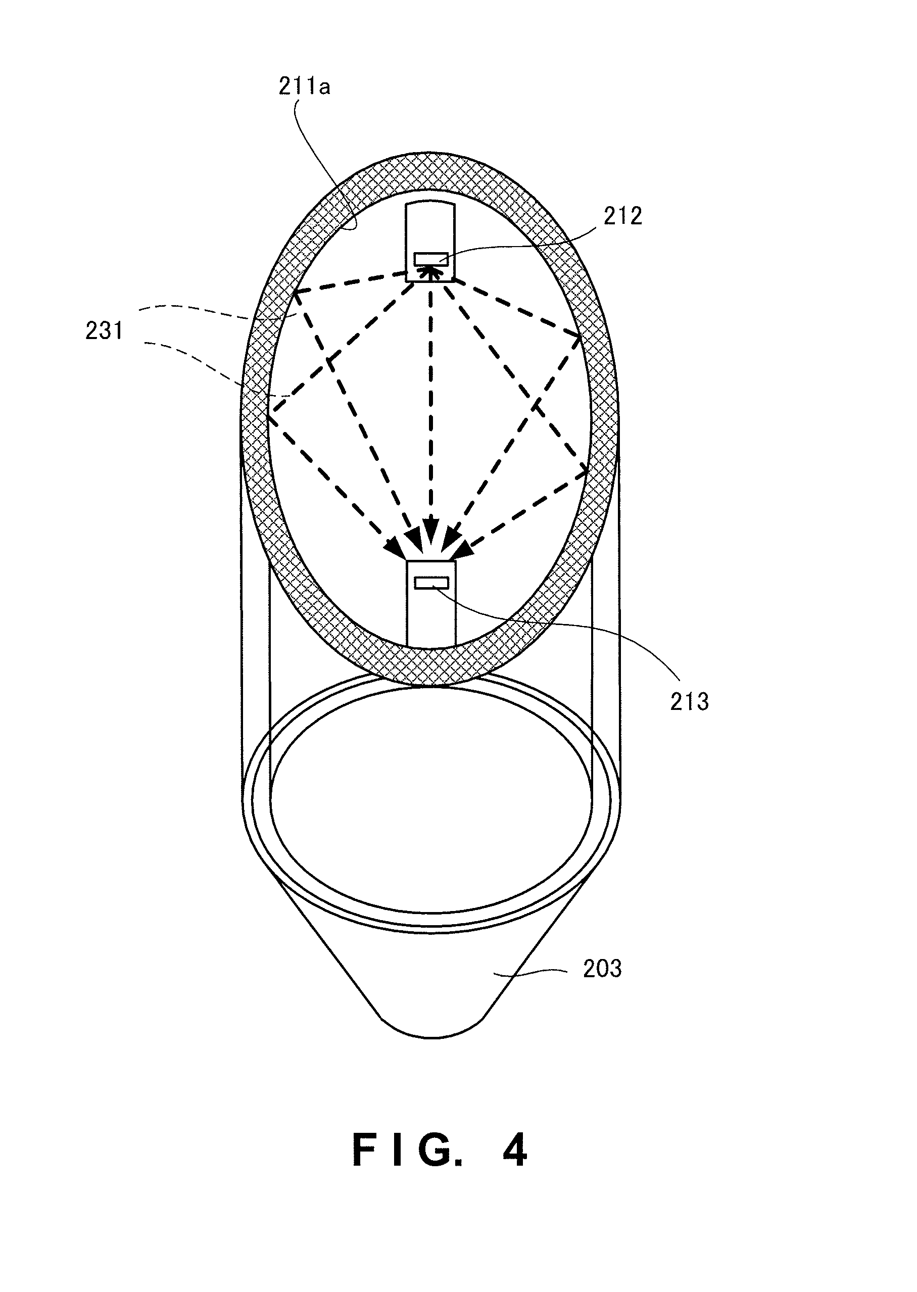
Next, the arrangement of the ray emitter 212 for inspection and the light receiver 213 will be described in detail with reference to FIGS. 3 to 5. FIG. 3 is a sectional view on a plane passing through the optical axis of the ray 205 for processing in the optical processing head 200. FIG. 4 is a sectional view taken along a line A-A in FIG. 3. The A-A section is a plane that is perpendicular to the optical axis of the ray 205 for processing and passes through the ray emitter 212 for inspection and the light receiver 213.
As is apparent from FIG. 4, the housing inner surface 211a draws an ellipse on the section passing through both the ray emitter 212 for inspection and the light receiver 213. The ray emitter 212 for inspection and the light receiver 213 are arranged at two focus positions of this ellipse. As is apparent from FIG. 4, the ray 231 for inspection emitted by the ray emitter 212 for inspection is reflected by the housing inner surface 211a, and almost all the ray 231 for inspection is collected to the light receiver 213.
As shown in FIG. 3, .theta. represents the angle of inclination, from the optical axis of the ray 205 for processing, of a line segment connecting the ray emitter 212 for inspection and the light receiver 213. L represents the distance (length of the line segment) between the ray emitter 212 for inspection and the light receiver 213. In this embodiment, the housing inner surface 211a has a columnar shape (columnar side surface) whose center axis is the optical axis of the ray 205 for processing. D represents the diameter of this column.
When .theta., L, and D defined in the above way satisfy equation (1), the ray emitter 212 for inspection and the light receiver 213 can be arranged at the two focuses of the ellipse: D/L=2/tan .theta. (1)
That is, equation (1) is a condition for arranging the ray emitter 212 for inspection and the light receiver 213 at the two focuses of the ellipse.
Theoretically, the light receiver 213 receives all the ray 231 for inspection emitted by the ray emitter 212 for inspection arranged to satisfy equation (1). In contrast, when the relation of equation (1) is not satisfied, a ray not received by the light receiver 213 exists.
FIG. 5 shows the relation of equation (1). The abscissa represents the inclination angle .theta., and the ordinate represents D/L. When .theta.=45.degree., D/L becomes about 2.
As described above, the second embodiment can provide an optical processing technique in which a trouble of the optical processing head that will be generated at the time of optical processing can be detected before the trouble occurs, by inspecting the contamination 241 of the inner surface of the circular cylindrical housing 211 or the concentration of the scattering object 242 flowing into the circular cylindrical housing 211.
Although the housing inner surface 211a has a shape conforming to the outer surface of the column in the above-described embodiment, the present invention is not limited to this. However, it is desirable that at least part of the housing inner surface 211a of the circular cylindrical housing 211 is a curved surface so that the ray 231 for inspection is reflected by the housing inner surface 211a of the circular cylindrical housing 211 and condensed to the light receiver 213.
Third Embodiment
An optical processing head 600 according to the third embodiment of the present invention will be described with reference to FIG. 6. FIG. 6 is a perspective view for explaining the internal arrangement of the optical processing head 600 according to this embodiment. FIG. 7 is a partial enlarged view. The optical processing head 600 according to the third embodiment is different from the optical processing head according to the second embodiment in that it includes an inspection unit 630 different in the inner surface shape from the inspection unit 230. The remaining arrangement and operation are the same as those in the second embodiment, so the same reference numerals denote the same arrangement and operation and a detailed description thereof will not be repeated.
The inspection unit 630 internally has a curved surface 631 of a shape conforming to the outer surface of a rotational ellipsoid. A ray emitter 612 for inspection and a light receiver 613 are arranged at two focus positions of the rotational ellipsoid. In this embodiment, no shielding plate need be provided around the ray emitter 612 for inspection. However, the shielding plate may also be provided. In this case, noise of a detection signal can be satisfactorily reduced.
FIG. 8 is a ray diagram between the ray emitter 612 for inspection and the light receiver 613 in the optical processing head 600 according to this embodiment. As is apparent from FIG. 8, the light receiver 613 receives all rays for inspection. That is, there is an effect of efficiently using inspection rays for inspection.
With the above-described arrangement, a line segment connecting the ray emitter 612 for inspection and the light receiver 613 can be perpendicular to the optical axis. Accordingly, the optical processing head 600 that is compact in the optical axis direction can be implemented.
Fourth Embodiment
An optical processing apparatus 900 according to the fourth embodiment of the present invention will be described with reference to FIG. 9. The optical processing apparatus 900 is an apparatus that includes one of the optical processing heads 100, 200, and 600 explained in the above-described embodiments, and generates a three-dimensional shaped object (or overlay welding) by melting a material by heat generated by condensed light. Here, the optical processing apparatus 900 including an optical processing head 200 will be explained as an example.
<<Apparatus Arrangement>>
In addition to the optical processing head 200, the optical processing apparatus 900 includes a light source 901, a light transmitting portion 210, a coolant supply device 903, a coolant supply portion 904, a stage 905, a material supply device 906, a material supply portion 907, a gas supply device 908, a gas supply portion 909, and a controller 930.
The light source 901 can be a laser, an LED, a halogen lamp, a xenon lamp, an incandescent lamp, or the like. The wavelength of a ray is, for example, 1,060 nm, but is not limited to this.
The coolant supply device 903 stores, for example, water as a coolant, and supplies the coolant by a pump to the optical processing head 200 via the coolant supply portion 904.
The coolant supply portion 904 is a resin or metal hose having an inner diameter of .PHI.2 to 6. The coolant is supplied into the optical processing head 200, circulated inside it, and returned to the coolant supply device 903, thereby suppressing the temperature rise of the optical processing head 200. The coolant supply amount is, for example, 1 to 10 L/min.
The stage 905 is, for example, an X stage, an X-Y stage, or an X-Y-Z stage, and can operate the respective axes (X, Y, and Z). The material supply device 906 supplies a material to a nozzle 203 via the material supply portion 907. Examples of the material are a metal particle, a resin particle, a metal wire, and a resin wire. The material supply device 906 can simultaneously supply even a carrier gas.
The material supply portion 907 is, for example, a resin or metal hose, and guides, to the nozzle 203, a powder flow prepared by mixing a material in a carrier gas. However, when the material is a wire, no carrier gas is necessary. The nozzle 203 ejects a material toward a process surface 260.
The gas supply device 908 supplies a purge gas to the optical processing head 200 through the gas supply portion 909. The purge gas is, for example, nitrogen, argon, or helium. However, the purge gas is not limited to this and may also be another gas as long as the purge gas is an inert gas. The purge gas supplied to the optical processing head 200 is ejected from the nozzle 203 along the above-described ray.
Although not shown, the optical processing apparatus 900 includes an orientation control mechanism and position control mechanism that control the orientation and position of the optical processing head 200.
<<Apparatus Operation>>
Next, the operation of the optical processing apparatus 900 will be explained. A shaped object 910 is created on the stage 905.
The purge gas is ejected from the nozzle 203 to the process surface 260. Thus, the peripheral environment of the molten pool is purged by the purge gas. By selecting an oxygen-free inert gas as the purge gas, oxidization of the process surface 260 can be prevented.
The optical processing head 200 is cooled by the coolant supplied from the coolant supply device 903 through the coolant supply portion 904, suppressing the temperature rise during processing.
By scanning the optical processing head 200 along the process surface 260 at the same time as the above-described series of operations, desired shaping can be performed while depositing the material. That is, this apparatus can implement overlay welding or three-dimensional shaping.
The controller 930 also functions as a purge controller that acquires, from the inspection unit 230, the status of a scattering object inside the optical processing head 200, controls the gas supply device 908 in accordance with this status, and changes the amount of a purge gas to be sprayed to the process surface 260.
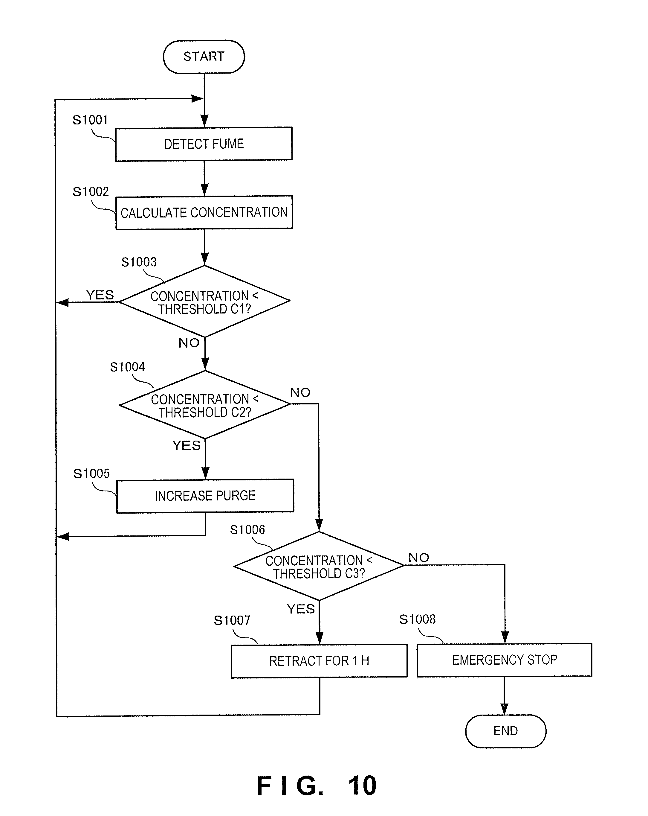
FIG. 10 is a flowchart showing the sequence of this control. This flowchart represents that four stages of control are performed in accordance with the amount of a scattering object by using three thresholds (threshold C1<threshold C2<threshold C3).
If a scattering object (fume) is detected in step S1001, the process advances to step S1002 to calculate the concentration. In step S1003, the calculated concentration is compared with the threshold C1. If the concentration is lower than the threshold C1, no problem occurs, so the process returns to step S1001. If the concentration is higher than the threshold C1, it is compared with another threshold C2 in step S1004. If the concentration is lower than the threshold C2, the process advances to step S1005 to cope with the scattering object by increasing the purge gas. If the concentration of the scattering object is higher than the threshold C2, the process advances to step S1006 to further compare the concentration with the threshold C3. If the concentration of the scattering object is lower than the threshold C3, the process advances to step S1007 to stop the optical processing apparatus 900 for 1 h or retract a workpiece for 1 h. If the concentration of the scattering object becomes higher than the threshold C3, the process advances to step S1008 to perform emergency stop.
As described above, according to the fourth embodiment, damage to a condensing optical system device 201 or the optical processing head 200 can be reduced.
Other Embodiments
The present invention has been described above with reference to the embodiments. However, the present invention is not limited to those embodiments. Various changes understandable by those skilled in the art within the scope of the present invention can be made for the arrangements and details of the present invention. The present invention also incorporates a system or apparatus that somehow combines different features included in the respective embodiments.
The present invention is applicable to a system including a plurality of devices or a single apparatus. The present invention is also applicable even when a control program for implementing the functions of the embodiments is supplied to the system or apparatus directly or from a remote site. Hence, the present invention also incorporates the program installed in a computer to implement the functions of the present invention on the computer, a medium storing the program, and a WWW (World Wide Web) server that causes a user to download the program. Especially, a non-transitory computer readable medium storing a program for causing a computer to execute processing steps included in the above-described embodiments falls within the scope of the present invention.
* * * * *
D00000
D00001
D00002
D00003
D00004
D00005
D00006
D00007
D00008
D00009
D00010
XML
uspto.report is an independent third-party trademark research tool that is not affiliated, endorsed, or sponsored by the United States Patent and Trademark Office (USPTO) or any other governmental organization. The information provided by uspto.report is based on publicly available data at the time of writing and is intended for informational purposes only.
While we strive to provide accurate and up-to-date information, we do not guarantee the accuracy, completeness, reliability, or suitability of the information displayed on this site. The use of this site is at your own risk. Any reliance you place on such information is therefore strictly at your own risk.
All official trademark data, including owner information, should be verified by visiting the official USPTO website at www.uspto.gov. This site is not intended to replace professional legal advice and should not be used as a substitute for consulting with a legal professional who is knowledgeable about trademark law.