Femtosecond laser-induced formation of submicrometer spikes on a semiconductor substrate
Mazur , et al.
U.S. patent number 10,361,083 [Application Number 14/836,609] was granted by the patent office on 2019-07-23 for femtosecond laser-induced formation of submicrometer spikes on a semiconductor substrate. This patent grant is currently assigned to President and Fellows of Harvard College. The grantee listed for this patent is President & Fellows Of Harvard College. Invention is credited to Eric Mazur, Mengyan Shen.


| United States Patent | 10,361,083 |
| Mazur , et al. | July 23, 2019 |
Femtosecond laser-induced formation of submicrometer spikes on a semiconductor substrate
Abstract
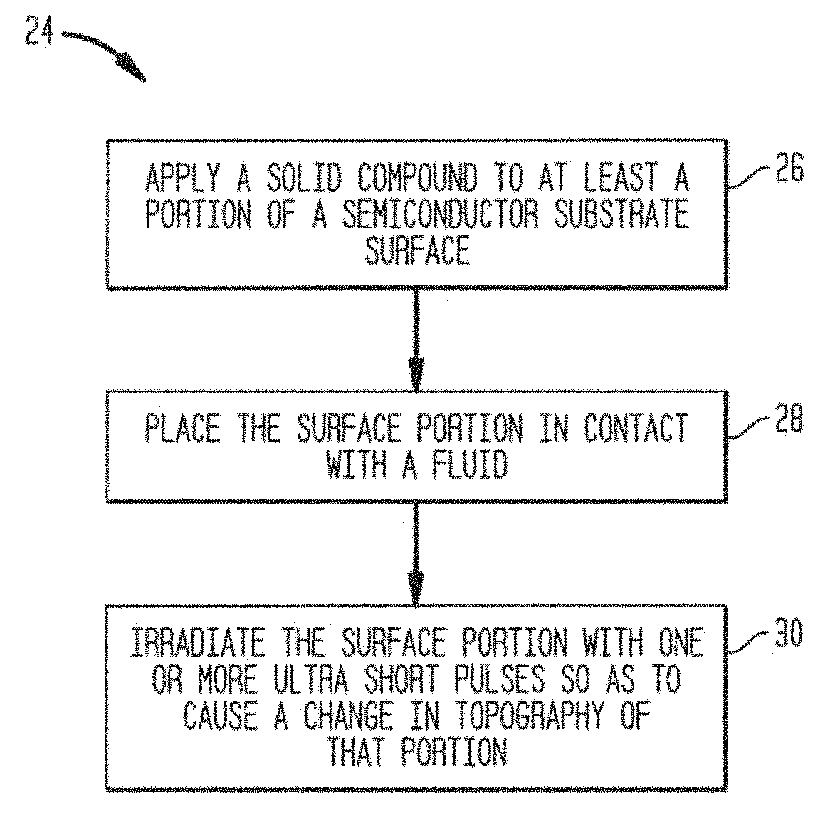
The present invention generally provides semiconductor substrates having submicron-sized surface features generated by irradiating the surface with ultra short laser pulses. In one aspect, a method of processing a semiconductor substrate is disclosed that includes placing at least a portion of a surface of the substrate in contact with a fluid, and exposing that surface portion to one or more femtosecond pulses so as to modify the topography of that portion. The modification can include, e.g., generating a plurality of submicron-sized spikes in an upper layer of the surface.
| Inventors: | Mazur; Eric (Concord, MA), Shen; Mengyan (Belmont, MA) | ||||||||||
|---|---|---|---|---|---|---|---|---|---|---|---|
| Applicant: |
|
||||||||||
| Assignee: | President and Fellows of Harvard
College (Cambridge, MA) |
||||||||||
| Family ID: | 41682662 | ||||||||||
| Appl. No.: | 14/836,609 | ||||||||||
| Filed: | August 26, 2015 |
Prior Publication Data
| Document Identifier | Publication Date | |
|---|---|---|
| US 20160005608 A1 | Jan 7, 2016 | |
Related U.S. Patent Documents
| Application Number | Filing Date | Patent Number | Issue Date | ||
|---|---|---|---|---|---|
| 14073460 | Nov 6, 2013 | 9136146 | |||
| 13021409 | Feb 4, 2011 | 8598051 | |||
| 12235086 | Sep 22, 2008 | 7884446 | |||
| 11196929 | Aug 4, 2005 | 7442629 | |||
| 10950230 | Sep 24, 2004 | 7057256 | |||
| 10950248 | Sep 24, 2004 | 7354792 | |||
| Current U.S. Class: | 1/1 |
| Current CPC Class: | H01L 29/30 (20130101); H01L 21/0259 (20130101); H01L 21/02381 (20130101); H01L 21/268 (20130101); H01L 21/302 (20130101); B23K 26/1224 (20151001); H01L 29/34 (20130101); H01L 21/02686 (20130101); H01L 21/67075 (20130101); H01L 21/02532 (20130101); H01L 21/2252 (20130101); Y10S 438/94 (20130101) |
| Current International Class: | B05D 3/06 (20060101); H01L 21/02 (20060101); H01L 21/225 (20060101); H01L 21/67 (20060101); H01L 21/268 (20060101); H01L 21/302 (20060101); B23K 26/12 (20140101) |
| Field of Search: | ;427/554,555,556,596,597 ;438/217,231,232,246-249,289-291,301-308 |
References Cited [Referenced By]
U.S. Patent Documents
| 3487223 | December 1969 | St. John |
| 3922571 | November 1975 | Smith |
| 3973994 | August 1976 | Redfield |
| 3994012 | November 1976 | Warner, Jr. |
| 4017887 | April 1977 | Davies et al. |
| 4105955 | August 1978 | Hayashi |
| 4149174 | April 1979 | Shannon |
| 4176365 | November 1979 | Kroger |
| 4181538 | January 1980 | Narayan et al. |
| 4201450 | May 1980 | Trapani |
| 4234358 | November 1980 | Celler |
| 4242149 | December 1980 | King et al. |
| 4253882 | March 1981 | Dalal |
| 4277793 | July 1981 | Webb et al. |
| 4322571 | March 1982 | Stanbery |
| 4343832 | August 1982 | Smith |
| 4346164 | August 1982 | Tabarelli et al. |
| 4419533 | December 1983 | Czubatyj et al. |
| 4452826 | June 1984 | Shields et al. |
| 4493942 | January 1985 | Sheng et al. |
| 4514582 | April 1985 | Tiedje et al. |
| 4536608 | August 1985 | Sheng et al. |
| 4546945 | October 1985 | Nessfield |
| 4568960 | February 1986 | Petroff et al. |
| 4593303 | June 1986 | Dyck et al. |
| 4593313 | June 1986 | Nagasaki et al. |
| 4617593 | October 1986 | Dudley |
| 4630082 | December 1986 | Sakai |
| 4648936 | March 1987 | Ashby et al. |
| 4663188 | May 1987 | Kane |
| 4672206 | June 1987 | Suzuki et al. |
| 4673770 | June 1987 | Mandelkom |
| 4679068 | July 1987 | Lillquist et al. |
| 4703996 | November 1987 | Glass et al. |
| 4723086 | February 1988 | Leibovich et al. |
| 4751571 | June 1988 | Lillquist |
| 4773944 | September 1988 | Nath et al. |
| 4775425 | October 1988 | Guha et al. |
| 4777490 | October 1988 | Sharma et al. |
| 4829013 | May 1989 | Yamazaki |
| 4838952 | June 1989 | Dill et al. |
| 4883962 | November 1989 | Elliott |
| 4886958 | December 1989 | Merryman et al. |
| 4887255 | December 1989 | Handa et al. |
| 4894526 | January 1990 | Bethea et al. |
| 4910568 | March 1990 | Takei et al. |
| 4910588 | March 1990 | Kinoshita et al. |
| 4964134 | October 1990 | Westbrook et al. |
| 4965784 | October 1990 | Land et al. |
| 4968372 | November 1990 | Maass |
| 4999308 | March 1991 | Nishiura et al. |
| 5021100 | June 1991 | Ishihara et al. |
| 5021854 | June 1991 | Huth |
| 5080725 | January 1992 | Green et al. |
| 5081049 | January 1992 | Green et al. |
| 5089437 | February 1992 | Shima et al. |
| 5100478 | March 1992 | Kawabata |
| 5101260 | March 1992 | Nath et al. |
| 5114876 | May 1992 | Weiner |
| 5127964 | July 1992 | Hamakawa et al. |
| 5164324 | November 1992 | Russell et al. |
| 5182231 | January 1993 | Hongo et al. |
| 5208822 | May 1993 | Haus et al. |
| 5223043 | June 1993 | Olson et al. |
| 5234790 | August 1993 | Lang et al. |
| 5236863 | August 1993 | Iranmanesh |
| 5244817 | September 1993 | Hawkins et al. |
| 5296045 | March 1994 | Banerjee et al. |
| 5309275 | May 1994 | Nishimura et al. |
| 5322988 | June 1994 | Russell et al. |
| 5346850 | September 1994 | Kaschmitter et al. |
| 5351446 | October 1994 | Langsdorf |
| 5370747 | December 1994 | Noguchi et al. |
| 5373182 | December 1994 | Norton |
| 5381431 | January 1995 | Zayhowski |
| 5383217 | January 1995 | Uemura |
| 5390201 | February 1995 | Tomono et al. |
| 5410168 | April 1995 | Hisa |
| 5413100 | May 1995 | Barthelemy et al. |
| 5449626 | September 1995 | Hezel |
| 5454347 | October 1995 | Shibata et al. |
| 5502329 | March 1996 | Pezzani |
| 5523570 | June 1996 | Hairston |
| 5559361 | September 1996 | Pezzani |
| 5569615 | October 1996 | Yamazaki et al. |
| 5569624 | October 1996 | Weiner |
| 5578858 | November 1996 | Mueller et al. |
| 5580615 | December 1996 | Itoh et al. |
| 5583704 | December 1996 | Fujii |
| 5589008 | December 1996 | Keppner |
| 5589704 | December 1996 | Levine |
| 5597621 | January 1997 | Hummel et al. |
| 5600130 | February 1997 | VanZeghbroeck |
| 5626687 | May 1997 | Campbell |
| 5627081 | May 1997 | Tsuo et al. |
| 5635089 | June 1997 | Singh et al. |
| 5640013 | June 1997 | Ishikawa et al. |
| 5641362 | June 1997 | Meier |
| 5641969 | June 1997 | Cooke et al. |
| 5705413 | January 1998 | Harkin et al. |
| 5705828 | January 1998 | Noguchi et al. |
| 5708486 | January 1998 | Miyawaki et al. |
| 5710442 | January 1998 | Watanabe et al. |
| 5714404 | February 1998 | Mitlitsky et al. |
| 5727096 | March 1998 | Ghirardi et al. |
| 5731213 | March 1998 | Ono |
| 5751005 | May 1998 | Wyles et al. |
| 5758644 | June 1998 | Diab et al. |
| 5766127 | June 1998 | Pologe et al. |
| 5766964 | June 1998 | Rohatgi et al. |
| 5773820 | June 1998 | Osajda et al. |
| 5779631 | July 1998 | Chance |
| 5781392 | July 1998 | Clark |
| 5792280 | August 1998 | Ruby et al. |
| 5802091 | September 1998 | Chakrabarti et al. |
| 5808350 | September 1998 | Jack et al. |
| 5859446 | January 1999 | Nagasu et al. |
| 5861639 | January 1999 | Bemier |
| 5871826 | February 1999 | Mei |
| 5898672 | April 1999 | Ginzboorg |
| 5923071 | July 1999 | Saito |
| 5935320 | August 1999 | Graef et al. |
| 5942789 | August 1999 | Morikawa |
| 5943584 | August 1999 | Shim et al. |
| 5963790 | October 1999 | Matsuno et al. |
| 5977515 | November 1999 | Uraki et al. |
| 5977603 | November 1999 | Ishikawa |
| 5995606 | November 1999 | Civanlar et al. |
| 6019796 | February 2000 | Mei |
| 6048588 | April 2000 | Engelsberg |
| 6049058 | April 2000 | Dulaney et al. |
| 6071796 | June 2000 | Voutsas |
| 6072117 | June 2000 | Matsuyama et al. |
| 6080988 | June 2000 | Ishizuya et al. |
| 6082858 | July 2000 | Grace et al. |
| 6097031 | August 2000 | Cole |
| 6106689 | August 2000 | Matsuyama |
| 6107618 | August 2000 | Fossum et al. |
| 6111300 | August 2000 | Cao et al. |
| 6128379 | October 2000 | Smyk |
| 6131511 | October 2000 | Wachi et al. |
| 6131512 | October 2000 | Verlinden et al. |
| 6147297 | November 2000 | Wettling et al. |
| 6160833 | December 2000 | Floyd et al. |
| 6168965 | January 2001 | Malinovich et al. |
| 6194722 | February 2001 | Fiorini et al. |
| 6204506 | March 2001 | Akahori et al. |
| 6229192 | May 2001 | Gu |
| 6242291 | June 2001 | Kusumoto et al. |
| 6252256 | June 2001 | Ugge et al. |
| 6272768 | August 2001 | Danese |
| 6290713 | September 2001 | Russell |
| 6291302 | September 2001 | Yu |
| 6313901 | November 2001 | Cacharelis |
| 6320296 | November 2001 | Fujii et al. |
| 6327022 | December 2001 | Nishi |
| 6331445 | December 2001 | Janz et al. |
| 6331885 | December 2001 | Nishi |
| 6333485 | December 2001 | Haight et al. |
| 6340281 | January 2002 | Haraguchi et al. |
| 6344116 | February 2002 | Warner, Jr. |
| 6372536 | April 2002 | Fischer et al. |
| 6372591 | April 2002 | Mineji et al. |
| 6372611 | April 2002 | Horikawa |
| 6379979 | April 2002 | Connolly |
| 6395624 | May 2002 | Bruce |
| 6420706 | July 2002 | Lurie et al. |
| 6429036 | August 2002 | Nixon et al. |
| 6429037 | August 2002 | Wenham et al. |
| 6457478 | October 2002 | Danese |
| 6465860 | October 2002 | Shigenaka et al. |
| 6475839 | November 2002 | Zhang et al. |
| 6479093 | November 2002 | Lauffer et al. |
| 6483116 | November 2002 | Kozlowski et al. |
| 6483929 | November 2002 | Murakami et al. |
| 6486046 | November 2002 | Fujimura et al. |
| 6486522 | November 2002 | Bishay et al. |
| 6493567 | December 2002 | Krivitski et al. |
| 6498336 | December 2002 | Tian et al. |
| 6500690 | December 2002 | Yamagishi et al. |
| 6504178 | January 2003 | Carlson et al. |
| 6562705 | May 2003 | Obara et al. |
| 6580053 | June 2003 | Voutsas |
| 6583936 | June 2003 | Kaminsky et al. |
| 6586318 | July 2003 | Lu |
| 6597025 | July 2003 | Lauter et al. |
| 6607927 | August 2003 | Ramappa et al. |
| 6624049 | September 2003 | Yamazaki |
| 6639253 | October 2003 | Duane et al. |
| 6667528 | December 2003 | Cohen et al. |
| 6677655 | January 2004 | Fitzergald |
| 6677656 | January 2004 | Francois |
| 6683326 | January 2004 | Iguchi et al. |
| 6689209 | February 2004 | Falster et al. |
| 6690968 | February 2004 | Mejia |
| 6734455 | May 2004 | Li |
| 6753585 | June 2004 | Kindt |
| 6759262 | July 2004 | Theil et al. |
| 6790701 | September 2004 | Shigenaka et al. |
| 6800541 | October 2004 | Okumura |
| 6801799 | October 2004 | Mendelson |
| 6803555 | October 2004 | Parrish et al. |
| 6815685 | November 2004 | Wany |
| 6818535 | November 2004 | Lu et al. |
| 6822313 | November 2004 | Matsushita |
| 6825057 | November 2004 | Heyers et al. |
| 6864156 | March 2005 | Conn |
| 6864190 | March 2005 | Han et al. |
| 6867806 | March 2005 | Lee et al. |
| 6876003 | April 2005 | Nakamura et al. |
| 6900839 | May 2005 | Kozlowski et al. |
| 6907135 | June 2005 | Gifford et al. |
| 6911375 | June 2005 | Guarini et al. |
| 6919587 | July 2005 | Ballon et al. |
| 6923625 | August 2005 | Sparks |
| 6927432 | August 2005 | Holm et al. |
| 6984816 | January 2006 | Holm et al. |
| 7008854 | March 2006 | Forbes |
| 7041525 | May 2006 | Clevenger et al. |
| 7057256 | June 2006 | Carey, III et al. |
| 7075079 | July 2006 | Wood |
| 7091411 | August 2006 | Falk et al. |
| 7109517 | September 2006 | Zaidi |
| 7112545 | September 2006 | Railkar et al. |
| 7118942 | October 2006 | Li |
| 7126212 | October 2006 | Enquist et al. |
| 7132724 | November 2006 | Merrill |
| 7202102 | April 2007 | Yao |
| 7211214 | May 2007 | Chou |
| 7211501 | May 2007 | Liu et al. |
| 7235812 | June 2007 | Chu et al. |
| 7247527 | July 2007 | Shimomura et al. |
| 7247812 | July 2007 | Tsao |
| 7256102 | August 2007 | Nakata et al. |
| 7271445 | September 2007 | Forbes |
| 7271835 | September 2007 | Iizuka et al. |
| 7285482 | October 2007 | Ochi |
| 7314832 | January 2008 | Kountz et al. |
| 7315014 | January 2008 | Lee et al. |
| 7354792 | April 2008 | Carey, III |
| 7358498 | April 2008 | Geng et al. |
| 7375378 | May 2008 | Manivannan et al. |
| 7390689 | June 2008 | Mazur et al. |
| 7432148 | October 2008 | Li et al. |
| 7442629 | October 2008 | Mazur |
| 7446359 | November 2008 | Lee et al. |
| 7446807 | November 2008 | Hong |
| 7456452 | November 2008 | Wells et al. |
| 7482532 | January 2009 | Yi et al. |
| 7498650 | March 2009 | Lauxtermann |
| 7504325 | March 2009 | Koezuka et al. |
| 7504702 | March 2009 | Mazur et al. |
| 7511750 | March 2009 | Murakami |
| 7521737 | April 2009 | Augusto |
| 7528463 | May 2009 | Forbes |
| 7542085 | June 2009 | Altice, Jr. et al. |
| 7547616 | June 2009 | Fogel et al. |
| 7551059 | June 2009 | Farrier |
| 7560750 | July 2009 | Niira et al. |
| 7564631 | July 2009 | Li et al. |
| 7569503 | August 2009 | Pan |
| 7582515 | September 2009 | Choi et al. |
| 7586601 | September 2009 | Ebstein |
| 7592593 | September 2009 | Kauffman et al. |
| 7595213 | September 2009 | Kwon et al. |
| 7605397 | October 2009 | Kindem et al. |
| 7615808 | November 2009 | Pain et al. |
| 7618839 | November 2009 | Rhodes |
| 7619269 | November 2009 | Ohkawa |
| 7629582 | December 2009 | Hoffman et al. |
| 7648851 | January 2010 | Fu et al. |
| 7649156 | January 2010 | Lee |
| 7705879 | April 2010 | Kerr et al. |
| 7728274 | June 2010 | Pilla et al. |
| 7731665 | June 2010 | Lee et al. |
| 7741666 | June 2010 | Nozaki et al. |
| 7745901 | June 2010 | McCaffrey et al. |
| 7763913 | July 2010 | Fan et al. |
| 7772028 | August 2010 | Adkisson et al. |
| 7781856 | August 2010 | Mazur et al. |
| 7800192 | September 2010 | Venezia et al. |
| 7800684 | September 2010 | Tatani |
| 7816220 | October 2010 | Mazur et al. |
| 7828983 | November 2010 | Weber et al. |
| 7847253 | December 2010 | Carey et al. |
| 7847326 | December 2010 | Park et al. |
| 7855406 | December 2010 | Yamaguchi et al. |
| 7875498 | January 2011 | Elbanhawy et al. |
| 7880168 | February 2011 | Lenchenkov |
| 7884439 | February 2011 | Mazur et al. |
| 7884446 | February 2011 | Mazur et al. |
| 7897942 | March 2011 | Bareket et al. |
| 7910391 | March 2011 | Alie |
| 7910964 | March 2011 | Kawahito et al. |
| 7923801 | April 2011 | Tian et al. |
| 7968834 | June 2011 | Veeder |
| 8008205 | August 2011 | Fukushima et al. |
| 8013411 | September 2011 | Cole |
| 8030726 | October 2011 | Sumi |
| 8035343 | October 2011 | Seman, Jr. |
| 8058615 | November 2011 | McCaffrey et al. |
| 8076746 | December 2011 | McCarten et al. |
| 8080467 | December 2011 | Carey, III et al. |
| 8088219 | January 2012 | Knerer et al. |
| 8093559 | January 2012 | Rajavel |
| 8164126 | April 2012 | Moon et al. |
| 8207051 | June 2012 | Sickler et al. |
| 8247259 | August 2012 | Grolier et al. |
| 8259293 | September 2012 | Andreou et al. |
| 8268403 | September 2012 | Akiyama et al. |
| 8288702 | October 2012 | Veeder |
| 8355545 | January 2013 | Corcoran et al. |
| 8445950 | May 2013 | Iida et al. |
| 8445985 | May 2013 | Hiyama et al. |
| 8456546 | June 2013 | Oike |
| 8530264 | September 2013 | De Munck et al. |
| 8603902 | December 2013 | Mazur |
| 8604405 | December 2013 | Liu et al. |
| 8649568 | February 2014 | Sato |
| 8679959 | March 2014 | Carey |
| 8698272 | April 2014 | Vineis |
| 8729678 | May 2014 | Shim |
| 8753990 | June 2014 | Gupta |
| 8802549 | August 2014 | Sickler |
| 8846551 | September 2014 | Gupta |
| 8928784 | January 2015 | Watanabe et al. |
| 9064762 | June 2015 | Yamaguchi |
| 9276143 | March 2016 | Mazur |
| 9478572 | October 2016 | Miyanami |
| 9559215 | January 2017 | Ahmed |
| 9659984 | May 2017 | Ohkubo et al. |
| 10121667 | November 2018 | Mazur |
| 2002/0034845 | March 2002 | Fujimura et al. |
| 2002/0081786 | June 2002 | Toet |
| 2002/0086502 | July 2002 | Liu |
| 2002/0126333 | September 2002 | Hosono et al. |
| 2002/0176650 | November 2002 | Zhao et al. |
| 2003/0025156 | February 2003 | Yamazaki et al. |
| 2003/0029495 | February 2003 | Mazur et al. |
| 2003/0045074 | March 2003 | Seibel |
| 2003/0132449 | July 2003 | Hosono et al. |
| 2004/0112426 | June 2004 | Hagino |
| 2004/0169834 | September 2004 | Richter et al. |
| 2005/0032249 | February 2005 | Im et al. |
| 2005/0063566 | March 2005 | Beek et al. |
| 2005/0127401 | June 2005 | Mazur et al. |
| 2005/0184291 | August 2005 | Cole et al. |
| 2005/0184353 | August 2005 | Mouli |
| 2005/0226287 | October 2005 | Shah et al. |
| 2006/0079062 | April 2006 | Mazur et al. |
| 2006/0102901 | May 2006 | Im et al. |
| 2006/0194419 | August 2006 | Araki |
| 2006/0231853 | October 2006 | Tanaka |
| 2007/0298533 | December 2007 | Yang et al. |
| 2008/0135099 | June 2008 | Yu |
| 2008/0191296 | August 2008 | Wang et al. |
| 2008/0251812 | October 2008 | Yoo |
| 2008/0303932 | December 2008 | Wang et al. |
| 2009/0036783 | February 2009 | Kishima |
| 2009/0090988 | April 2009 | Ohgishi |
| 2009/0096049 | April 2009 | Oshiyama et al. |
| 2009/0151785 | June 2009 | Naum et al. |
| 2009/0200625 | August 2009 | Venezia et al. |
| 2009/0273695 | November 2009 | Mabuchi |
| 2009/0278967 | November 2009 | Toumiya |
| 2010/0108864 | May 2010 | Ohta et al. |
| 2010/0128161 | May 2010 | Yamaguchi |
| 2010/0171948 | July 2010 | Mazur et al. |
| 2010/0190292 | July 2010 | Alberts |
| 2010/0201834 | August 2010 | Maruyama et al. |
| 2010/0213582 | August 2010 | Coullard et al. |
| 2010/0270635 | October 2010 | Sickler |
| 2011/0025842 | February 2011 | King et al. |
| 2011/0150304 | June 2011 | Abe et al. |
| 2011/0241148 | October 2011 | Hiyama et al. |
| 2011/0241152 | October 2011 | Hsiao et al. |
| 2012/0001841 | January 2012 | Gokingco et al. |
| 2012/0025199 | February 2012 | Chen et al. |
| 2012/0049306 | March 2012 | Ohba et al. |
| 2012/0147241 | June 2012 | Yamaguchi et al. |
| 2012/0153127 | June 2012 | Hirigoyen et al. |
| 2012/0153128 | June 2012 | Roy et al. |
| 2012/0188431 | July 2012 | Takimoto |
| 2012/0217602 | August 2012 | Enomoto |
| 2012/0228473 | September 2012 | Yoshitsugu |
| 2013/0020468 | January 2013 | Mitsuhashi et al. |
| 2013/0026531 | January 2013 | Seo et al. |
| 2013/0082343 | April 2013 | Fudaba et al. |
| 2013/0207212 | August 2013 | Mao et al. |
| 2014/0054662 | February 2014 | Yanagita et al. |
| 2014/0273535 | September 2014 | Gupta |
| 2014/0374868 | December 2014 | Lee et al. |
| 2017/0141258 | May 2017 | McFarland |
| 2017/0244920 | August 2017 | Ohkubo et al. |
| 2018/0083146 | March 2018 | Mazur |
| 2018/0151361 | May 2018 | Mazur |
| 3666484 | Jun 1985 | AU | |||
| 1507075 | Jun 2004 | CN | |||
| 1614789 | May 2005 | CN | |||
| 101053065 | Oct 2007 | CN | |||
| 101241923 | Aug 2008 | CN | |||
| 101404307 | Apr 2009 | CN | |||
| 101423942 | May 2009 | CN | |||
| 101465361 | Jun 2009 | CN | |||
| 101478013 | Jul 2009 | CN | |||
| 101634026 | Jan 2010 | CN | |||
| 101634027 | Jan 2010 | CN | |||
| 101740597 | Jun 2010 | CN | |||
| 101818348 | Sep 2010 | CN | |||
| 201725796 | Jan 2011 | CN | |||
| 101978498 | Feb 2011 | CN | |||
| 102270646 | Dec 2011 | CN | |||
| 19838439 | Apr 2000 | DE | |||
| 0473439 | Mar 1992 | EP | |||
| 0566156 | Oct 1993 | EP | |||
| 1 347 670 | Sep 2003 | EP | |||
| 1347670 | Sep 2003 | EP | |||
| 1630871 | Mar 2006 | EP | |||
| 1873840 | Jan 2008 | EP | |||
| 2073270 | Jun 2009 | EP | |||
| 2509107 | Oct 2012 | EP | |||
| 2827707 | Jan 2003 | FR | |||
| 2030766 | Apr 1980 | GB | |||
| S5771188 | May 1982 | JP | |||
| S57173966 | Oct 1982 | JP | |||
| S63116421 | May 1988 | JP | |||
| H02152226 | Jun 1990 | JP | |||
| H02237026 | Sep 1990 | JP | |||
| H03183037 | Aug 1991 | JP | |||
| H04318970 | Nov 1992 | JP | |||
| 1994-244444 | Sep 1994 | JP | |||
| H06244444 | Sep 1994 | JP | |||
| H06267868 | Sep 1994 | JP | |||
| H06275641 | Sep 1994 | JP | |||
| H0774240 | Mar 1995 | JP | |||
| H07183484 | Jul 1995 | JP | |||
| H07235658 | Sep 1995 | JP | |||
| 9148594 | Jun 1997 | JP | |||
| H09298308 | Nov 1997 | JP | |||
| 11077348 | Mar 1999 | JP | |||
| 11097724 | Apr 1999 | JP | |||
| 2000164914 | Jun 2000 | JP | |||
| 2001024936 | Jan 2001 | JP | |||
| 2001189478 | Jul 2001 | JP | |||
| 2001257927 | Sep 2001 | JP | |||
| 2001339057 | Dec 2001 | JP | |||
| 2002043594 | Feb 2002 | JP | |||
| 2002134640 | May 2002 | JP | |||
| 2002513176 | May 2002 | JP | |||
| 2002-190386 | Jul 2002 | JP | |||
| 2003058269 | Feb 2003 | JP | |||
| 2003104121 | Apr 2003 | JP | |||
| 2003163360 | Jun 2003 | JP | |||
| 2003242125 | Aug 2003 | JP | |||
| 2003258285 | Sep 2003 | JP | |||
| 2003308130 | Oct 2003 | JP | |||
| 2004047682 | Feb 2004 | JP | |||
| 2004273886 | Sep 2004 | JP | |||
| 2004273887 | Sep 2004 | JP | |||
| 2005072097 | Mar 2005 | JP | |||
| 2005339425 | Dec 2005 | JP | |||
| 2006033493 | Feb 2006 | JP | |||
| 2006147991 | Jun 2006 | JP | |||
| 2006173381 | Jun 2006 | JP | |||
| 2006210701 | Aug 2006 | JP | |||
| 2006255430 | Sep 2006 | JP | |||
| 2006261372 | Sep 2006 | JP | |||
| 2007122237 | May 2007 | JP | |||
| 2007135005 | May 2007 | JP | |||
| 2007165909 | Jun 2007 | JP | |||
| 2007180642 | Jul 2007 | JP | |||
| 2007180643 | Jul 2007 | JP | |||
| 2007305675 | Nov 2007 | JP | |||
| 2008099158 | Apr 2008 | JP | |||
| 2008153361 | Jul 2008 | JP | |||
| 2008167004 | Jul 2008 | JP | |||
| 2008181468 | Aug 2008 | JP | |||
| 2008187003 | Aug 2008 | JP | |||
| 2008283219 | Nov 2008 | JP | |||
| 2008294698 | Dec 2008 | JP | |||
| 2009021479 | Jan 2009 | JP | |||
| 2009026142 | Feb 2009 | JP | |||
| 2009152569 | Jul 2009 | JP | |||
| 2009206356 | Sep 2009 | JP | |||
| 2009253683 | Oct 2009 | JP | |||
| 2010226071 | Oct 2010 | JP | |||
| 2010278472 | Dec 2010 | JP | |||
| 2011003860 | Jan 2011 | JP | |||
| 2011091128 | May 2011 | JP | |||
| 2012054321 | Mar 2012 | JP | |||
| 2012169530 | Sep 2012 | JP | |||
| 2012212349 | Nov 2012 | JP | |||
| 20010061058 | Jul 2001 | KR | |||
| 2005039273 | Apr 2005 | KR | |||
| 20060020400 | Mar 2006 | KR | |||
| 20080014301 | Feb 2008 | KR | |||
| 20080097709 | Nov 2008 | KR | |||
| 20090077274 | Jul 2009 | KR | |||
| 20100026463 | Mar 2010 | KR | |||
| 20100118864 | Nov 2010 | KR | |||
| 20110079323 | Jul 2011 | KR | |||
| 20170070266 | Jun 2017 | KR | |||
| 200627675 | Aug 2006 | TW | |||
| 200818529 | Apr 2008 | TW | |||
| 9114284 | Sep 1991 | WO | |||
| 2000031679 | Jun 2000 | WO | |||
| 0131842 | May 2001 | WO | |||
| 0131842 | May 2001 | WO | |||
| 0135601 | May 2001 | WO | |||
| 0135601 | May 2001 | WO | |||
| 2002041363 | May 2002 | WO | |||
| 2003059390 | Jul 2003 | WO | |||
| 2005029599 | Mar 2005 | WO | |||
| WO 2005/029599 | Mar 2005 | WO | |||
| 2006043690 | Apr 2006 | WO | |||
| 2006054758 | May 2006 | WO | |||
| 2006086014 | Aug 2006 | WO | |||
| 2008091242 | Jul 2008 | WO | |||
| 2008099524 | Aug 2008 | WO | |||
| 2008145097 | Dec 2008 | WO | |||
| 2009016846 | Feb 2009 | WO | |||
| 2009100023 | Aug 2009 | WO | |||
| 2009147085 | Dec 2009 | WO | |||
| 2010033127 | Mar 2010 | WO | |||
| 2011003871 | Jan 2011 | WO | |||
| 2011035188 | Mar 2011 | WO | |||
| 2011119618 | Sep 2011 | WO | |||
| 2012027290 | Mar 2012 | WO | |||
| 2012117931 | Sep 2012 | WO | |||
| 2012174752 | Dec 2012 | WO | |||
| 2014110484 | Jul 2014 | WO | |||
Other References
|
Nayak et al.; "Femtosecond Laser-Induced Micro-Structuring of Thin a-Si:H Films"; Material Research Society symposium proceedings; vol. 850; Nov. 28-Dec. 2, 2004; pp. MM1.8.1-MM1.8.5. cited by examiner . Shen et al., "Formation of Regular Arrays of Silicon Microspikes by Femtosecond Laser Irradiation Through a Mask", Appl. Phys. Lett., 82, 1715-1717, Mar. 1, 2003. cited by applicant . Younkin et al., "Infrared Absorption by Conical Silicon Microstructures Made in a Variety of Backgroun Gases Using Femtosecon-Laser Pulses", J. Appl. Phys., 93, 2626-2629, Mar. 1, 2003. cited by applicant . Wu, C. et al., "Black Silicon a New Light Absorber," APS Centennial Meeting (Mar. 23, 1999). cited by applicant . Wu et al. "Visible Luminescence From Silicon Surfaces Microstructured in Air", Appl. Phys. Lett., 81, 1999-2001, Sep. 2002. cited by applicant . Carey et al., "High Sensitivity Silicon-Based VIS/NIR Photodetectors", Optical Society of America (2003) 1-2. cited by applicant . Solar Energy Research Institute, "Basic Photovoltaic Principles and Methods," Van Nostrand Reinhold Co., NY 1984, pp. 45-47 and 138-142, no author available. cited by applicant . Wu et al., "Near-Unity Below-Band Gap Absorption by Microstructured Silicon", Appl. Phys. Lett., 78, 1850-1852, vol. 78, No. 13; Mar. 26, 2001. cited by applicant . Her et al., "Ferntosecond Laser-Induced Formation of Spikes on Silicon", Appl. Phys. A., 70, 383-385 (2000), published online Mar. 8. cited by applicant . Her et al., "Microstructuring of Silicon With Femtosecond Laser Pulses", Appl. Phys. Lett., 73, 1673-1675 Sep. 21, 1998. cited by applicant . Carey et al., "High Sensitivity Silicon-Based VIS/NIR Photodetectors", CLEO 2004 (San Francisco, CA, 2004) 1-2. cited by applicant . Serpenguzel et al., "Temperature Dependence of Photoluminescence in Non-Crystalline Silicon", Photonics West (SAn Jose, CA 2004) 454-462. cited by applicant . Carey et al., "Femtosecond Laser-Assisted Microstructuring of Silicon for Novel Detector, Sensing and Display Technologies", LEOS 2002 (Glasgow, Scotland, 2002) 97-98. cited by applicant . Younkin et al., "Infrared Absorption by Conical Silicon Microstructures Made in a Variety of Background Gases Using Femtosecond-Laser Pulses", CLEO 2001 (Baltimore, MD 2001) 556-556. cited by applicant . Carey et al., "Femtosecon-Laser-Assisted Microstructuring of Silicon Surfaces", Optics and Photonics News, 14, 32-36 Feb. 2003. cited by applicant . Younkin, "Surface Studies and Microstructure Fabrication Using Ferntosecond Laser Pulses", Ph.D. Thesis, Harvard University, 2001 118 pages, Aug. cited by applicant . Wu, "Femtosecond Laser-Gas-Solid Interactions", Ph.D. Thesis, Harvard University, 2000, 135 pages, August. cited by applicant . Sanchez et al., "Dynamics of the Hydrodynamical Growth of Columns on Silicon Exposed to ArF Excimer-Laser Irradiation", Appl. Phys. A, 66, 83-86 (1998). cited by applicant . Sanchez et al., "Whiskerlike Strucutre Growth on Silicon Exposed to ArF Excimer Laser Irradiation", Appl. Phys. Lett., 69 (5), 620-622, Jul. 1996. cited by applicant . Pedraza et al., "Surface Nanostructuring of Silicon", Appl Phys. A. 77, 277-284 (2003). cited by applicant . Fowlkes et al., "Surface Microstructuring and Long-Range Ordering of Silicon Nanoparticles", Appl. Phys. Lett., 80 (20), 3799-3801, May 2002. cited by applicant . Dolgaev et al., "Formation of Conical Microstructures Upon Laser Evaporation of Solids", Appl. Phys. A, 73, 177-181 (2001), published online Jun. 20, 2001. cited by applicant . Pedraza et al., "Silicon Microcolumn Arrays Grown by Nanosecond Pulsed-Excimer Laser Irradiation", Appl. Phys. Lett. 74 (16), 2322-2324, Apr. 1999. cited by applicant . Hu et al., "Solar Cells from Basic to Advanced Systems," McGraw Hill Book Co., NY 1983, p. 39. cited by applicant . Carey, et al., "Fabrication of Micrometer-Sized Conical Field Emitters Using Femto-second Laser-Assisted Etching of Silicon," Proc. IVMC2001 (Davis, CA 2001) 75-76 (2001). cited by applicant . Carey, et al., "Field emission from Silicon Microstructures Formed by Femtosecond Laser Assisted Etching, "Proc. CLEO 2001 (Baltimore, MD 2001) 555-557. cited by applicant . Crouch et al., "Infrared Absorption by Sulfur-Doped Silicon Formed by Femtosecond Laser Irradiation", App. Phys. A. 79, 1635-1641 (2004), published online Jun. 23, 2004. cited by applicant . Her et al., "Novel Conical Microstructures Created in Silicon With Femtosecond Laser Pulses", CLEO 1998 (San Francisco, CA 1998) 511-512, May. cited by applicant . Crouch, et al., "Comparison of structure and properties of femtosecond and nanosecond laser-structured silicon" Applied Physics Letters, AIP, American Institute of Physicls, vol. 84, No. 11 (Mar. 15, 2004), pp. 1850-1852. cited by applicant . Carey, et al., "Femtosecond laser-assisted microstructuring of silicon for novel detector, sensing and display technologies", Electro-Optics Society, IEEE, vol. 1 (Oct. 26, 2003), pp. 481-482. cited by applicant . L. van der Zel, "SF6 and the Environment," EPRI, Nov. 2003. cited by applicant . Office Action for U.S. Appl. No. 14/100,954 dated Jul. 21, 2015. cited by applicant . Bernard, C.G. "Structural and Functional Adaptation in a Visual System", Endeavor, vol. XXVI (May 1967); pp. 79-84. cited by applicant . Clapham, P.B. et al. "Reduction of Lens Reflexion by the "Moth Eye" Principle", Nature Vo. 244 (Aug. 3, 1973) pp. 281-282. cited by applicant . Hansen, Henri et al. "The Black Silicon Method: A Universal Method for determining the Parameter Setting of a Fluorine-Based Reactive Ion Etcher in Depp Silicon Trench Etching With Profile Control", J. Micromedch. Microeng. 5 (1'995) pp. 115-120. cited by applicant . Zhu, Jing-Tao et al., "Effect of Polarization on Femtosecond Laser Pulses Structuring Silicon Surface", Applied Surface Science, 252, pp. 275-2756 (2006), published online Jun. 13, 2005. cited by applicant . Huang, M. et al. "A Uniform 290 nm Periodic Square Stucture on ZnO Fabricated by Two-Beam Femtosecond Laser Ablation", Nanotechnology 18, pp. 1-6, Nov. 20, 2007. cited by applicant . International Search Report, Written Opinion for PCT Application No. PCT/US09/25239, date of completion Apr. 23, 2009; dated May 8, 2009. cited by applicant . Bouhdada, A. et al. "Modeling of the Spectral Response of PIN Photodetectors Impact of Exposed Zone Thickness, Surface Recombination Velocity and Trap Concentration", Microelectronics Reliability 44, pp. 223-228 (2004). cited by applicant . Vigue, F. and Faurie, J.P. "Zn(MgBe)Se Ultraviolet Photodetectors" Journal of Electronic Materials, vol. 30, No. 6, pp. 662-226 (2001), (no month, but after Feb. 4, 2001). cited by applicant . European Search Report for European Patent Application No. 09015646.4, date of completion of search Apr. 15, 2010. cited by applicant . Sidebottom, G. et al. "SS7 MTP3-User Adaptation Layer (M3UA)", Netwok Working Group--Internet-Draft, pp. 1-96, (editor) Feb. 2001. cited by applicant . Morneault, K. et al. "User Adaptation Layer", ISDN Q. 921, Network Working Group, pp. 1-66 (Feb. 2001), The Internet Society request for comments: 3057. cited by applicant . European Search Report for European Patent Application No. 012019515, date of completion of Search Oct. 30, 2001. cited by applicant . Ong, L. et al. "Framework Architecture for Signaling Transport", Network Working Group, pp. 1-24 (Oct. 1999), The Internet Society request for comments: 2719. cited by applicant . Stewart, R. et al. "Stream Control Transmission Protocol", Network Working Group, pp. 1-134 (Oct. 2000), The Internet Society request for comments: 2960. cited by applicant . Park et al., "Deep Trench Isolation for Crosstalk Suppression in Active Pixel Sensors with 1.7.mu.m Pixel Pitch", in Japanese Journal of Applied Physics, vol. 46, No. 4B, pp. 2454-5457, Apr. 24, 2007. cited by applicant . Payne, D.N.R. et al.; Characterization of Experimental Textured ZnO:Al Films for Thin Film Solar Cell Applications and Comparison with Commercial and Plasmonic Alternatives; Photovoltaic Specialists Conference (PVSC); pp. 1560-1564; 2010; IEEE. cited by applicant . Rao, et al., Monolithic and Fully-Hybrid Backside Illuminated CMOS Imagers for Smart Sensing, IMEC, Kapeldreef 75, B-3001 Leuven, Belgium, 4 pages. cited by applicant . Rashkeev et al., "Hydrogen passivation and Activation of Oxygen Complexes in Silicon," Applied Physics Letters; American Institute of Physics, vol. 78(11), pp. 1571-1573 (Mar. 12, 2001). cited by applicant . Russell, et al.; "Nanosecond Eximer Laser Processing for Novel Microelectronic Fabrication"; Nanosecond Excimer Laser Processing; 6 pages; 1989, pp. 228-233. cited by applicant . Russell, Ramirez, Kelley, "Nanosecond Excimer Laser Processing for Novel Microelectronic Fabrication," SSC Pacific Technical Reports , pp. 228-233, 2003, vol. 4, US Navy. cited by applicant . Sai, H. et al.; Enhancement of Light Trapping in Thin-Film Hydrogenated Microcrystalline Si Solar Cells Using Back Reflectors with Self-Ordered Dimple Pattern; Applied Physics Letters; vol. 93; 2008; American Institute of Physics, Published online Oct. 8, 2008; pp. 143501-to 143501-3. cited by applicant . Sarnet et al.; "Femtosecond laser for black silicon and photovoltaic cells"; Feb. 21, 2008, Proc. of SPIE; vol. 6881; pp. 1-15, pp. 688119(1-15). cited by applicant . Senoussaoui, N. et al.; Thin-Film Solar Cells with Periodic Grating Coupler; Thin Solid Films; pp. 397-401; 2004; Elsevier B.V. cited by applicant . Serpenguzel et al., "Temperature Dependence of Photluminescence in Non-Crystalline Silicon", Photonics West (San Jose, CA, 2004) 454-462. cited by applicant . Solhusvik, J. et al. "A 1280.times.960 3.75.mu.m pixel CMOS imager with Triple Exposure HDR," Proc. of 2009 International Image Sensor Workshop, Bergen, Norway, Jun. 22-28, 2009. cited by applicant . STMicroelctronics, BSI--technical challenges, IISW-2009, Bergen. Jun. 25, 2009, 37 pages, (Set of lecture view graphs). cited by applicant . Stone et al.; The X-ray Sensitivity of Amorphous Selenium for Mammography;.Am. Assoc. Phys. Med.; Mar. 2002; pp. 319-324; vol. 29 No. 3. cited by applicant . Szlufcik, J. et al.; Simple Integral Screenprinting process for selective emitter polycrystalline silicon solar cells; Applied Physics Letters; vol. 59, No. 13; Sep. 23, 1991; American Institute of Physics, pp. 1583-1584. cited by applicant . Takayanagi, et al.; "A 600..times..600 Pixel, 500, fps CMOS Image Sensor with a 4.4.mu.m Pinned Photodiode 5-Transistor Global Shutter Pixel"; 2007 International Image Sensor Workshop; Jun. 6-10, 2007. cited by applicant . Tournier, et al., Pixel-to-Pixel isolation by Deep Trench technology, STMicroelectronics, 850, rue Jean Monnet--F-38926 Crolles Cedex--France, 2011, 4 pages, June. cited by applicant . Tournier, et al., Pixel-to-Pixel isolation by Deep Trench technology: Application to CMOS Image Sensor, https://www.researchgate.net/publication/268300742, 2011, 5 pages. cited by applicant . Tower, John R. et al.; Large Format Backside Illuminated CCD Imager for Space Surveillance; IEEE Transactions on Electron Devices, vol. 50, No. 1; Jan. 2003; pp. 218-224. cited by applicant . Uehara et al., "A High-Sensitive Digital Photosensor Using MOS Interface-Trap Charge Pumping," IEICE Electronics Express, 2004, vol. 1, No. 18, 556-561, Dec. 26. cited by applicant . Wilson, "Depth Distributions of Sulfur Implanted Into Silicon as a Function of Ion energy, Ion Fluence, and Anneal Temperature,", Journal Applied Physics, 55(10); May 15, 1984, pp. 3490-3494. cited by applicant . Winderbaum, S. et al.; Reactive ion etching (RIE) as a method for texturing polycrystalline silicon solar cells; Solar Energy Materials and Solar Cells; 1997; pp. 239-248; Elsevier Science B.V. cited by applicant . Wu et al., "Black Silicon, A New Light Absorber" Harvard UPS 1999, APS Centennial Meeting Mar. 23, 1999. cited by applicant . Xiong , Y., et al, "Depth from focusing and defocusing", Computer Vision and Pattern Recognition, 1993. Proceedings CVPR '93., 1993 IEEE , Los Alamitos, CA, USA.IEEE Comput. Soc, Jun. 15, 1993 (Jun. 15, 1993), pp. 68-73. cited by applicant . Xu, Y., et al, "Infrared Detection Using Thermally Isolated Diode," Sensors and Actuators A, Elsevier Sequoia S.A., 1993, vol. 36, 209-217, Lausanne, Switzerland. cited by applicant . Yamamoto, K. et al.; NIR Sensitivity Enhancement by Laser Treatment for Si Detectors; Nuclear Instruments and Methods in Physics Research A; pp. 520-523; Mar. 31, 2010; Elsevier. cited by applicant . Yan, B. et al.; Light Trapping Effect from Randomized Textures of Ag/ZnO Back Reflector on Hyrdrogenated Amorphous and Nanocrystalline Silicon Based Solar Cells; Thin Film Solar Technology II--Proceedings of SPIE vol. 7771; 2010; SPIE, pp. 777102(1-7). cited by applicant . Yasutomi, et al.; "Two-Stage Charge Transfer Pixel Using Pinned Diodes for Low-Noise Global Shutter Imaging"; 2009 International Image Sensor Workshop; Mar. 28, 2009. cited by applicant . Yaung et al., "High performance 300mm backside illumination technology for continuous pixel shrinkage," IEEE 2011 International Electron Devices Meeting, Washington, DC, 2011, pp. 8.2.1-8.2.4, or pp. IEDMII--(175-178). cited by applicant . Yuan, et al.; "Efficient black silicon solar cell with a density-graded nanoporous surface: Optical properties, performance limitations, and design rules"; American Institute of Physics; Applied Physics Letters 95. 1230501 (2009) 3 pages, vol. 95. cited by applicant . Zaidi, S.H. et al.; Diffraction Grating Structures in Solar Cells; Photovoltaic Specialists Conference, 2000; 4 pages; Sep. 2000; IEEE. cited by applicant . Zhang et al, "Ultra-Shallow P+-Junction Formation in Silicon by Excimer Laser Doping: a Heat and Mass Transfer Perspective," Int. J. Heat Mass Transfer, 1996, 3835-3844, vol. 39, No. 18, Elsevier Science Ltd., Great Britain. cited by applicant . Zhong, S. et al. "All-Solution-Processed Random Si Nanopyramids for Excellent Light Trapping in Ultrathin Solar Cells," AFM-Joumal, May 2016 pp. 1-11. cited by applicant . Zhu et al., "Evolution of Silicon Surface Microstructures by Picosecond and Femtosecond Laser Irradiations," Applied Surface Science, 2005, 102-108, Elsevie, Amsterdam, NL, Available online Nov. 2004. cited by applicant . Ziou et al., "Depth from defocus using the hermite transform", Image Processing, 1998. ICIP 98. Intl. Conference on Chicago, IL. Oct. 1998 pp. 958-962, IEEE. cited by applicant . Shah et al., Thin-film silicon solar cell technology. Progress in Photovoltaics 12, 113-142 (2004). cited by applicant . Sheehy et al., Chalcogen doping of silicon via intense femtosecondlaser irradiation. Materials Science and Engineering B-Solid State Materials for Advanced Technology 137, 289-294 (2007). cited by applicant . Sheehy et al., Role of the Background Gas in the Morphology and Optical Properties of Laser-Microstructured Silicon. Chem Mater. 2005; 17(14):3582-6. cited by applicant . Shockley et al., Detailed Balance Limit ofEfficiency of p-n Junction Solar Cells. Journal of Applied Physics 32,510-519, Mar. 1961; vol. 32, No. 3. cited by applicant . Sidebottom, G. et al., "SS7 MTP3-User Adaptation Layer (M3UA)," Network Working Group, Internet Draft, The Internet Engineering Task Force, pp. 1-128, (Feb. 2001). cited by applicant . Sipe et al., Laser-Induced Periodic Surface-Structure .1. Theory. Physical Review B 27, 1141-1154 (1983), vol. 27, No. 2; Jan. 15. cited by applicant . Slaoui et al., Advanced inorganic materials for photovoltaics. Mrs Bulletin 32, 211-218, Mar. 2007. cited by applicant . Solar Energy Research Institute, "Basic Photovoltaic Principles and Methods," Van Nostrand Reinhold Co., NY 1984, pp. 45-47 and 138-142. cited by applicant . Staebler et al., Stability of n-i-p Amorphous-Silicon Solar-Cells. Applied Physics Letters 39, 733-735 (1981), vol. 3, No. 9; Nov. 1. cited by applicant . Stalmans et al. Porous silicon in crystalline silicon solar cells: A review and the effect on the internal quantum efficiency. Progress in Photovoltaics 6 233-246 ( 1998), vol. 6; pp. 233-246. cited by applicant . Stupca et al., Enhancement of polycrystalline silicon solar cells using ultrathin films of silicon nanoparticle. Applied Physics Letters 91, 063107 (2007), pp. 063107(1-3); Aug. 6, 2007. cited by applicant . Svrcek et al., Ex situ prepared Si nanocrystals embedded in silica glass: Formation and characterization. Journal of Applied Physics 95, 3158-3163 (2004), vol. 95, No. 6; Mar. 15. cited by applicant . Svrcek et al., Silicon nanocrystals as light converter for solar cells. Thin Solid Films vol. 451-452, pp. 384-388 (2004). cited by applicant . Tabbal et al., "Formation of Single Crystal Sulfur Supersaturated Silicon Based Junctions by Pulsed Laser Melting". 2007, J. Vac. Sci. Technol. B25(6), 1847-1852. cited by applicant . Tiwari et al., A silicon nanocrystals based memory. Applied Physics Letters 68, 1377-1379 (1996), vol. 86, No. 10; Mar. 4. cited by applicant . Torres et al., Device grade microcrystalline silicon owing to reduced oxygen contamination, Applied Physics Letters 69, 1373-1375 (1996), Issue 10. cited by applicant . Tsing-Hua Her, "Femtochemistry at gas/solid interfaces", The Division of Engin. and Appl. Sciences, Harvard University Cambridge, Massachusetts, May, 1998, pp. 138. cited by applicant . Tull et al., Formation of silicon nanoparticles and web-like aggregates by femtosecond laser ablation in a background gas. Applied Physics A; Materials Science & Processing 83, 341-346, Mar. 1, 2006. cited by applicant . Tull et al., Silicon surface morphologies after femtosecond laser irradiation, MRS Bulletin 31, 626-633, Aug. 2006. cited by applicant . Tull; "Femtosecond Laser Ablation of Silicon: Nanoparticles, Doping and Photovotaics"; Harvard University, Jun. 2007 (Thesis). cited by applicant . Vigue, F. et al. "Zn (MgBe) Se ultraviolet photodetectors" Journal of Electronic Materials, vol. 30, No. 6, pp. 662-666 (2001). cited by applicant . Wilson et al., Quantum Confinement in Size-Selected, Surface-Oxidized Silicon Nanocrystals. Science 262, 1242-1244, Nov. 19, 1993. cited by applicant . Wronski, Electronic Properties of Amorphous Silicon in Solar-Cell Operation; IEEE Transactions on Electron Devices 24, 351-357, Apr. 1977, vol. 24, No. 4. cited by applicant . Wu et al., "13.9%--efficient CdTe polycrystalline thin-film solar cells with an infrared transmission of.about.50%", Progress in Photovoltaics 14, 471-483 (2006). cited by applicant . Wu, et al "Near-Unity Below-Band-Gap Absorption by Microstructured Silicon," 2001, Applied Physics Letters, 1850-1852, vol. 78, No. 13, American Institute of Physics, Mar. 26. cited by applicant . Yablonovitch, et al.; "Intensity Enhancement in Textured Optical Sheets for Solar Cells"; .COPYRGT. 1982 IEEE. cited by applicant . Yu et al., Polymer Photovoltaic CellsEnhanced Efficiencies via a Network ofIntemal Donor-Acceptor Heterojunctions. Science 270, 1789-1791, Dec. 15, 1995. cited by applicant . Zhao et al., 19.8% efficient "honeycomb" textured multicrystalline and 24.4% monocrystalline silicon solar cells. Applied Physics Letters 73, 1991-1993 (1998), vol. 73, No. 14; Oct. 5, 1998; pp. 1991-1993. cited by applicant . Huang, M. et al. "A Uniform 290 nm Periodic Square Stucture on ZnO Fabricated by Two-Beam Femtosecond Laser Ablation", Nanotechnology 18, pp. 1-6 (2007), pp. 505301(1-6); Nov. 20. cited by applicant . Stewart, R. et al. "Stream Control Transmission Protocol", Network Working Group, pp. 1-134 (Oct. 2000). cited by applicant . Aberle, Progress with polycrystalline silicon thin-film solar cells on glass at UNSW. Journal of Crystal Growth 287,386-390, Jan. 4, 2006. cited by applicant . Amoruso et al., Emission of nanoparticles during ultrashort laser irradiation of silicon targets. Europhysics Letters 67, 404-410, Aug. 1, 2004 vol. 67, No. 3. cited by applicant . Arango et al., Charge transfer in photovoltaics consisting of interpenetrating networks of conjugated polymer and Ti02 nanoparticles. Applied Physics Letters 74, 1698-1700 (1999), vol. 74, No. 12; Mar. 22. cited by applicant . Beek et al., Efficient hybrid solar cells from zinc oxide nanoparticles and a conjugated polymer. Advanced Materials 16, 1009-1013, Jun. 2004 vol. 16, No. 12. cited by applicant . Bentini et al., Surface doping of semiconductors by pulsed-laser irradiation in reactive atmosphere. Applied Physics A: 1988;45(4):317-324, Solids & surfaces. cited by applicant . Blood et al., Electrical Characterization of Semiconductors. Reports on Progress in Physics 41, 157-257 (1978). cited by applicant . Bouhada, A. et al. "Modeling of the Spectral Response of PIN Photodetectors Impact of Exposed Zone Thickness, Surface Recombination Velocity and Trap Concentration", Microelectronics Reliability 44, pp. 223-228 (2004). cited by applicant . Brus, Luminescence of Silicon Materials-Chains, Sheets, Nanocrystals, Nanowires, Microcrystals, and Porous Silicon. Journal of Physical Chemistry 98,3575-3581 (1994). cited by applicant . Bucksbaum et al., Rapid Melting and Regrowth Velocities in Silicon Heated by Ultraviolet Picosecond Laser-Pulses, Physical Review Letters 53, 182-185 (1984), vol. 53, No. 2; Jul. 9. cited by applicant . Bulgakov et al., Silicon clusters roduced by femtosecond laser ablation: non-thermal emission and gas-phase condensation. Applied Physics A; Materials Science & Processing 79, 1591-1594, Jul. 26, 2004. cited by applicant . Campbell et al., Light Trapping Properties of Pyramidally Textured Surfaces. Journal of Applied Physics 62, 243-249, Jul. 1, 1987. cited by applicant . Cifre, et al. Polycrystalline Silicon Films Obtained by Hot-Wire Chemical-Vapor-Deposition. Applied Physics 59, 645-651 (1994). cited by applicant . Contreras et al., Progress toward 20% efficiency in Cu(In,Ca)Se-2 polycrystalline thin-film solar cells. Progress in Photovoltaics 7, 311-316 (1999). cited by applicant . Curtins et al., High-Rate Deposition of Amorphous Hydrogenated Silicon-Effect of Plasma Excitation-Frequency. Electronics Letters 23, (1987), Issue 5; Feb. 26, 1987; only abstract of article supplied. cited by applicant . Delley et al., Quantum Confinement in Si Nanocrystals. Physical Review B 47, 1397-1400 (1993), vol. 47, No. 3; Jan. 15. cited by applicant . Dolgaev et al., "Formation of Conical Microstructures Upon Laser Evaporation of Solids", Appl. Phys. A, 2001, 73, 177-181, Published online Jun. 20, 2001. cited by applicant . Fowlkes et al., "Surface Microstructuring and Long-Range Ordering of Silicon Nanoparticles", Appl. Phys. Lett., 2002, 80 (20), 3799-3801, May 20. cited by applicant . Glezer et al., Ultrafast-laser driven micro-explosions in transparent materials. Applied Physics Letters 71, 882-884, Aug. 18, 1997. cited by applicant . Glover et al., Probing paiticle synthesis during femtosecond laser ablation: initial phase transition kinetics. Applied Physics B Lasers and Optics 78, 995-1000, Apr. 7, 2004. cited by applicant . Glover, Hydrodynamics of particle formation following femtosecond laser ablation. Journal of the Optical Society of America B-Optical Physics 20, 125-131 (2003), vol. 20, No. 1; January. cited by applicant . Goetzberger et al., Crystalline Silicon Solar Cells (ed.), Chapter 6, High Efficiency Solar Cells. New York: John Wiley& Sons Ltd, 1994. cited by applicant . Green, Recent developments in photovoltaics. Solar Energy 76, 3-8 (2004). cited by applicant . Greenham et al.,Charge sepai-ation and transport in conjugatedpolymerjsemiconductor-nanocrystal composites studied by photoluminescence quenching and photoconductivity. Physical Review B 54, 17628-17637 (1996), vol. 54, No. 24; Dec. 15. cited by applicant . Halls et al., Efficient Photodiodes from Interpenetrating Polymer Networks. Nature 376, 498-500, Aug. 1995. cited by applicant . Heisterkamp et al., Pulse energy dependence of subcellular dissection by femtosecond laser pulses. Optics Express 13, 3690-3696 (2005), vol. 13, No. 10; May 16. cited by applicant . Henry, Limiting Efficiencies of Ideal Single and Multiple Energy Gap Terrestrial Solar-Cells. Journal of Applied Physics 51, 4494-4500, Aug. 1980 vol. 51(8). cited by applicant . Hu et al., "Solar Cells from Basic to Advanced Systems," McGraw Hill Book Co., 1983, p. 39, New York, New York. cited by applicant . Huang, et al.; "Microstructured silicon photodetector"; Applied Physics Letters 89, 033506; 2006 American Institute of Physics, Jul. 20, 2006; pp. 033506(1-3). cited by applicant . Keppner et al., Passivation Properties of Amorphous and Microcrystalline Silicon Layers Deposited by VHF-GD for Crystalline Silicon Solar-Cells. Solar Energy Materials and Solar Cells 34, 201-209 (1994). cited by applicant . Kim et al.; "Strong Sub-Band-Gap Infrared Absorption in Silicon Supersaturated with Sulfur"; 2006 Appl. Phys. Lett. 88, 241902-1-241902-3, Published online Jun. 12, 2006. cited by applicant . Luque et al., Increasing the efficiency of ideal solar cells by photon induced transitions at intermediate levels. Physical Review Letters 78, 5014-5017 (1997), vol. 78, No. 26; Jun. 30. cited by applicant . Marti et al., Limiting efficiencies for photovoltaic energy conversion in multigap systems. Solar Energy Materials and Solar Cells 43, 203-222 (1996). cited by applicant . Meier et al., Recent progress in micromorph solar cells. Journal of Non-Crystalline Solids, 1250-1256 (1998), vol. 227-230. cited by applicant . Meier etal., Complete Microcrystalline p-i-n. SolarCell-Crystalline or Amorphous Cell Behavior? Applied Physics Letters 65, 860-862 (1994), vol. 65, No. 7; Aug. 15. cited by applicant . Mo et al., Sulfur point defects in crystalline and amorphous silicon. Physical Review B 70 (2004), Nov. 19; pp. 205210(1-10). cited by applicant . Morneault, K. et al., "ISDN Q.921-User Adaptation Layer," Network Working Group, Request for Comments: 3057, The Interent Society, pp. 1-66, (2001 ), February. cited by applicant . Morneault, K. et al., "SS7 MTP2-User, Adaptation Layer," Network Working Group, Internet Draft, The Internet Engineering Task Force, pp. 1-4, (Feb. 2001), 1-56 pages actually provided, with internal p. 1-33. cited by applicant . Myers et al., Enhancing near-infrared avalanche photodiode performance by femtosecond laser microstructuring. Applied Optics 45, 8825-8831 (2006), vol. 45, No. 35; Dec. 10. cited by applicant . Nirmal et al., Lwninescence photophysics in semiconductor nanocrystals. Accounts of Chemical Research 32. 407-414 (1999), Published on web Nov. 25, 1998. cited by applicant . O'Regan et al., A Low-Cost, High-Efficiency Solar-Cell Based on DyeSensitized Colloidal TiO2 Films. Nature 353, 737-740, Oct. 24, 1991. cited by applicant . Pavesi et al., Optical gain in silicon nanocrystals. Nature 408, 440-444, Nov. 23, 2000. cited by applicant . Rath et al., Limited influence of grain boundary defects in hot-wire CVD polysilicon films on solar cell performance. Journal of Non-Crystalline Solids, 1277-1281 (1998), vol. 227-230. cited by applicant . Reber et al., Crystalline silicon thin-film solar cellsrecent results at Fraunhofer ISE, Solar Energy 77, 865-875, Oct. 14, 2004. cited by applicant . Samet et al., Laser doping for microelectronics and microtechnology. Proc.of SPIE vol. 5448 pp. 669-680, (SPIE, Bellingham, WA 2004). cited by applicant . Schaffer et al., Micromachining bulk glass by use of femtosecond laser pulses with nanojoule energy. Optics Letters, vol. 26, No. 2; 93-95, Jan. 15, 2001. cited by applicant . Schuppler et al., Size, Shape, and Composition of Luminescent Species in Oxidized Si Nanocrystals and H-Passivated Porous Si. Physical Review B 52, 4910-4925 (1995). cited by applicant . Seto, Electrical Properties of Polydystalline Silicon Films. Jomnal of Applied Physics, 5247-5254 (1975), vol. 46, No. 12; December. cited by applicant . http://joseph-tang.blogspot.com/2017/, Oshiyama et al. , Near-infrared Sensitivity Enhancement of a Back-illuminated Complementary Metal Oxide Semiconductor Image Sensor with a Pyramid Surface for Diffraction Structure,(2017). cited by applicant . Huang, et al.; "Key Technique for texturing a uniform pyramid structure with a layer of silicon nitride on monocrystalline silicon wafer" Applied Surface Science; 2013 pp. 245-249, vol. 266. cited by applicant . Hupkes, J. et al.; Light Scattering and Trapping in Different Thin Film Photovoltaic Devices; 24th European Photovoltaic Solar Energy Conference, Hamburg, Germany (Sep. 21-25, 2009); pp. 2766-2769. cited by applicant . Ingalson et al. Defect States in the CIGS Solar cells by Photocapacitance and Deep Level Optical Spectroscopy; Bulletin of the Polish Academy of Sciences Technical Sciences; 2005; pp. 157-161; vol. 53(2). cited by applicant . IMEC, 3D Integrated Image Sensors for Smart Imaging Systems, Piet De Moor, 2010, 32 pages. cited by applicant . Itonaga et al., "Extremely-low-noise CMOS Image Sensor with high saturation capacity," 2011 International Electron Devices Meeting, Washington, DC, 2011, pp. 8.1.1-8.1.4, IEEE. cited by applicant . Job et al., "Doping of Oxidized Float Zone Silincon by Thermal Donors--A low Thermal Budget Doping Method for Device Applications?" Mat. Res. Soc. Symp. Pro.; v. 719, F9.5.1-F9.5.6 (2002). cited by applicant . Joy, T. et al.; Development of a Production-Ready, Back-Illuminated CMOS Image Sensor with Small Pixels; Electron Devices Meeting; pp. 1007-1010; 2007; IEEE. cited by applicant . Fan Ji et al.; Advanced Photodiode Detector for Medical CT Imaging: Design and Performance; 2007; pp. 2730-2735; IEEE. cited by applicant . Kitamura et al., "Suppression of crosstalk by using backside deep trench isolation for 1.12.mu.m backside illuminated CMOS image sensor," 2012 International Electron Devices Meeting, San Francisco, CA, 2012, pp. 24.2.1-24.2.4. cited by applicant . Koh et al., "Simple nanostructuring on silicon surfaceby means of focused beam patterning and wet etching", Applied Surface Science, 2000 pp. 599-603, vol. 162-163. cited by applicant . Kolasinski et al., "Laser Assisted and Wet Chemical Etching of Silicon Nanostructures," J. Vac. Sci. Technol., A 24(4), Jul./Aug. 2006, 1474-1479. cited by applicant . Konstantatos et al., "Engineering the Temproal Response of Photoconductive Photodetectors via Selective Introduction of Surface Trap States," Nano Letters, v. 8(5), pp. 1446-1450 (Apr. 2, 2008). cited by applicant . Konstantatos et al., "PbS Colloidal Quantum Dot Photoconductive Photodetectors: Transport, Traps, and Gain," Appl. Phys. Lett., v. 91, pp. 173505-1-173505-3 (Oct. 23, 2007). cited by applicant . Korean Intellectual Property Office (KIPO), CMOS Image Sensor, KIPO, 2004, 29 pages. cited by applicant . Kray, D. et al.; Laser-doped Silicon Soalr Cells by Laser Chemical Processing (LCP) exceeding 20% Efficiency; 33rd IEEE Photovoltaic Specialist Conference; 3 pages; May 2008; IEEE. cited by applicant . Kroning et al.; X-ray Imaging Systems for NDT and General Applications; 2002; Fraunhofer Institute for Nondestructive Testing; Saarbrucken and Dresden, Germany, National Seminar of ISNT, Dec. 5-7, 2002. cited by applicant . Krymski; A High Speed 4 Megapixel Digital CMOS Sensor; 2007 International Image Sensor Workshop; Jun. 6-10, 2007, pp. 78-81. cited by applicant . Lee et al., SNR Performance Comparison of 1.4um Pixel : FSI, Light-guide, and BSI, 2011, 3 pages. (No publication source). cited by applicant . Li et al., "Gettering in High Resistive Float Zone Silicon Wafers for Silicon Detector Applications" Transaction on Nuclear Science, vol. 36(1), pp. 290-294 (Feb. 1, 1989). cited by applicant . Li, "Design and Simulation of an Uncooled Double-Cantilever Microbolometer with the Potential for ..about..mK NETD," 2004, Sensors and Actuators A, pp. 351-359, vol. 112, Elsevier B.V. cited by applicant . Li, Hongsong et al.; An experimental study of the correlation between surface roughness and light scattering for rough metallic surfaces; Advanced Characterization Techniques for Optics, Semiconductors, and Nanotechnologies II; 2005; pp. 25780V-1-25780V-15; vol. 5878; SPIE Bellingham, WA. cited by applicant . Lin, A. et al.; Optimization of Random Diffraction Gratings in Thin-Film Solar Cells Using Genetic Algorithms; 2007; 1 page; SSEL Annual Report. cited by applicant . Low Dose Technologies; Power Point. cited by applicant . Madzharov, et al.; "Light trapping in thin-firm silicon solar cells for superstrate and substrate configuration" Abstract #1614, 218.sup.th ECS Meeting .COPYRGT. 2010 the Electrochemical Society. cited by applicant . "Masimo Rainbow SET Pulse CO-Oximetry," 2010, Masimo Corporation, Irvine, California, //www.masimo.com/Rainbow/about.htm. cited by applicant . Mateus; C.F.R. et al.; Ultrabroadband Mirror Using Low-Index Cladded Subwavelength Grating; Photonics Technology Letters; vol. 16, Issue No. 2; pp. 518-520; Feb. 2004; IEEE. cited by applicant . Matsuno, Shigeru et al.; Advanced Technologies for High Efficiency Photovoltaic Systems; Mitsubishi Electric Advance; vol. 122; pp. 17-19; Jun. 2008, Technical Reports. cited by applicant . Meynants, et al.; "Backside illuminated global shutter COMOS image sensors"; 2011 International Image Sensor Workshop; Jun. 11, 2011, (4 pages). cited by applicant . Minoglou et al., "Reduction of Electrical Crosstalk in Hybrid Backside Illuminated CMOS Imagers using Deep Trench Isolation," 2008 International Interconnect Technology Conference, Burlingame, CA, USA, 2008, pp. 129-131. cited by applicant . Moloney, A.M. et al.; Novel Black Silicon PIN Photodiodes; 8 pages; Jan. 25, 2006; SPIE. cited by applicant . Moon et al. Selective emitter using porous silicon for crystalline silicon solar cells. Solar Energy Materials & Solar Cells, v. 93, pp. 846-850 (2009), Nov. 17, 2008. cited by applicant . Moses; Nuclear Medical Imaging--Techniques and Challenges; Power Point; Feb. 9, 2005; Lawrence Berkeley National Laboratory Department of Functional Imaging. cited by applicant . Munday, J.N. et al.; Large Integrated Absorption Enhancement in Plasmonic Solar Cells by Combining Metallic Gratings and Antireflection Coatings; Nano Letters; vol. 11, No. 6; pp. 2195-2201; Oct. 14, 2010; American Chemical Society. cited by applicant . Murkin, JM and Arangol, M, "Near Infrared spectroscopy as an index of rain and tissue oxygenation," Bri. J. of Anathesia (BJA/PGA Supplement):13-iI3 (2009), Oxford Journal of Medicine & BJA; vol. 103, issue supplement 1; p. i3-i13. cited by applicant . Myers, Richard et al., "Enhancing Near-IR Avalanche Photodiodes Performance by Femtosecond Laser Microstructuring" Harvard Dept. of Physics. (No publication source or date, but newest citation 2006, thus this year or later). cited by applicant . Nauka et al., "New Intrinsic Gettering Process in Silicon Based on Interactions of Silicon Interstitials," J. App. Phys., vol. 60(2), pp. 615-621, Jul. 15, 1986. cited by applicant . Nauka et al., Intrinsic Gettering in Oxygen-Free Silicon; App. Phys. Lett., vol. 46(7), Apr. 1, 1985, pp. 673-675. cited by applicant . Nayak et al, "Semiconductor Laesr Crystallization of a--Si:H," SPIE Digital Library, 2003, vol. 4977, Bellingham, Washington. 2003, pp. 377-380. cited by applicant . Nayak et al, "Semiconductor Laser Crystallization of a--Si:H on Conducting Tin-Oxide-Coated Glass for Solar Cell and Display Applications," Applied Physics A, 2005, 1077-1080, Springer Berlin, Heidelberg, Germany, vol. 80. cited by applicant . Nayak et al, "Ultrafast-Laser-Assisted Chemical Restructuring of Silicon and Germanium Surfaces," Applied Surface Science, 2007, 6580-6583, vol. 253, Issue 15, Elsevier B.V, Published online Jan. 30, 2007. cited by applicant . Nayak, B.K. et al.; Ultrafast Laser Textured Silicon Solar Cells; Mater. Res. Soc. Symp. Proc.; vol. 1123; 6 pages; 2009; Materials Research Society. cited by applicant . Nayak, et al.; "Efficient light trapping in silicon solar cells by ultrafast-laser-induced self-assembled micro/nano structures"; Progress in Photovoltaics: Research and Applications; 2011, (9 pages). cited by applicant . Oden, et al.; "Optical and Infrared Detection Using Microcantilevers;" SPIE Digital Library downloaded on Oct. 13, 2010; vol. 2744; 10 pages, pp. 345-354. cited by applicant . Ohring, Milton "The Materials of Science of Thin Films"--pp. 176-179; Academic Press, 1992, (Excerpt, "4.6 CVD Processes and Systems"). cited by applicant . Pain, Bedabrata; "A Back-Illuminated Megapixel CMOS Image Sensor"; hdl.handle.net/2014/39312; May 1, 2005, (4 pages). cited by applicant . Pain, Bedabrata; Backside Illumination Technology for SOI-CMOS Image Sensors; 2009 IISW Symposium on Backside Illujination of Solid-State Image Sensors, Bergen Norway; Jun. 25, 2009; pp. 1-23. cited by applicant . Palm et al. CIGSSe Thin Film PB Modules: From Fundamental Investigators to Advanced Performance and Stability; Thin Solid Films; 2004; pp. 544-551; vol. 451-2. cited by applicant . A. Arndt, J.F. Allison, J.G. Haynos, and A. Meulenberg, Jr., "Optical Properties of the COMSAT Non-reflective Cell," 11th IEEE Photovoltaic Spec. Conf., p. 40, 1975, pp. 40-43. cited by applicant . Agranov, et al., Pixel continues to shrink . . . Small Pixels for Novel CMOS Image Sensors, 4 pages, (No date, but after 2009, cited reference; no publication source). cited by applicant . Asom et al., Interstitial Defect Reactions in Silicon; Appl. Phys. Lett.; Jul. 27, 1987; pp. 256-258; vol. 51(4); American Institute of Physics. cited by applicant . Berger, Michael; Moth Eyes Inspire Self-Cleaning Antireflection Nanotechnology Coatings; 3 pages; Nanowerk LLC, "Copyright 2008 nanowerkLLC" (no actual publication date or source). cited by applicant . Berger, O., Inns, D. and Aberle, A.E. "Commercial White Paint as Back Surface Reflector for Thin-Film Solar Cells", Solar Energy Materials & Solar Cells, vol. 91, pp. 1215-1221, May 8, 2007. cited by applicant . Betta et al.; Si-PIN X-Ray Detector Technology; Nuclear Instruments and Methods in Physics Research A; 1997; pp. 344-348; vol. 395; Elsevier Science B.V. cited by applicant . Boden, S.A. et al.; Nanoimprinting for Antireflective Moth-Eye Surfaces; 4 pages; 2008. cited by applicant . Bogue: "From bolometers to beetles: the development of the thermal imaging sensors;" sensor Review; 2007; pp. 278-281; Emerald Group Publishing Limited (ISSN 0260-2288). cited by applicant . Borghesi et al.; "Oxygen Precipitation in Silicon," J. Appl. Phys., v. 77(9), pp. 4169-4244 (May 1, 1995). cited by applicant . Born, M. and E.Wolf, "Princip les of Optics, 7th Ed.", Cambridge University Press, 1999, pp. 246-255. cited by applicant . Brieger,S., O.Dubbers, S.Fricker, A.Manzke, C.Pfahler, A.Plettl, and P.Zlemann, "An Approach for the Fabrication of Hexagonally Ordered Arrays of Cylindrical Nanoholes in Crystalline and Amorphous Silicon Based on the Self-Organization of Polymer Micelles", Nanotechnology, vol. 17, pp. 4991-4994, 2006, doi:10.1088/0957-4884/17/19/036, Sep. 15. cited by applicant . Buttgen, B.; "Demodulation Pixel Based on Static Drift Fields"; IEEE Transactions on Electron Devices, vol. 53, No. 11, Nov. 2006. cited by applicant . Campbell, Stephen A., "The Science and Engineering of Microelectronic Fabrication,2nd Ed.", Oxford University Press, 2001, pp. 406-411, (Excerpt from book). cited by applicant . Carey, III; "Femtosecond-laser Microstructuring of Silicon for Novel Optoelectronic Devices"; Harvard University, 2004; (Thesis), July. cited by applicant . Carey, P.G. et al., "In-situ Doping of Silicon Using Gas Immersion Laser Doping (GILD) Process," Appl. Surf. Sci. 43, 325-332 (1989). cited by applicant . Chang, S.W., V.P.Chuang, S.T.Boles, and C.V.Thompson, "Metal-Catalyzed Etching of Vertically Aligned Polysilicon and Amorphous Silicon Nanowire Arrays by Etching Direction Confinement", Advanced Functional Materials, vol. 20, No. 24, pp. 4364-4370, 2010. cited by applicant . Chen, Q. et al.; Broadband moth-eye antireflection coatings fabricated by low-cost nanoimprinting; Applied Physics Letters 94; pp. 263118-1-263118-3; 2009; American Institute of Physics, Jul. 2. cited by applicant . Chiang, Wen Jen Et al., "Silicon Nanocrystal-Based Photosensor on Low-Temperature Polycrystalline-Silicon Panels", Applied Physics Letters, 2007, 51120-1-51120-3, vol. 91, American Inst. of Physics, Melville, NY, Aug. 2. cited by applicant . Chichkov, B.N. et al, "Femtosecond, picosecond and nanosecond laser ablation of solids" Appl. Phys. A 63, 109-115; 1996. cited by applicant . Chien et al, "Pulse Width Effect in Ultrafast Laser Processing of Materials," Applied Physics A, 2005, vol. 81; pp. 1257-1263, Springer Berlin, Heidelberg, Germany, Published online Aug. 31, 2004. cited by applicant . Choubey et al., On Evolution of CMOS Image Sensors, Proceedings of the 8th International Conference on Sensing Technology, Sep. 2-4, 2014, Liverpool, UK, pp. 89-94. cited by applicant . Cilingiroglu et al., "An evaluation of MOS Interface-Trap Charge Pump as and Ultralow Constant-Current Generator," IEEE Journal of Solid-State Circuit, 2003, vol. 38, No. 1, Jan. 2003, 71-83. cited by applicant . Cmosis; "Global Shutter Image Sensors for Machine Vision Application"; Image Sensors Europe 2010, Mar. 23-25, 2010; .COPYRGT. copyright 2010, (Set of view graphs). cited by applicant . Cotter, Jeffrey E.; Optical intensity of light in layers of silicon with rear diffuse reflectors; Journal of Applied Physics; Jul. 1, 1998; pp. 618-624; vol. 84, No. 1; American Institute of Physics. cited by applicant . Despeisse, et al.; "Thin Film Silicon Solar Cell on Highly Textured Substrates for High Conversion Efficiency"; (No publication source; most recent citation is 2010, so given date is impossible). cited by applicant . Detection of X-ray and Gamma-ray Photons Using Silicon Diodes; Dec. 2000; Detection Technology, Inc.; Micropolis, Finland. cited by applicant . Dewan, Rahul et al.; Light Trapping in Thin-Film Silicon Solar Cells with Submicron Surface Texture; Optics Express; vol. 17, No. 25; Dec. 7, 2009; Optical Society of America. cited by applicant . Deych et al.; Advances in Computed Tomography and Digital Mammography; Power Point (Viewgrahs) ; ISMART; Nov. 18, 2008; Analogic Corp.; Peabody, MA. cited by applicant . Dobie, et al.; "Minimization of reflected light in photovoltaic modules"; Mar. 1, 2009. www.renewableenergyworld.com/real news/?unintelligible/2009/03/miniaturization-of-reflected-light-in-photov- oltaic-modules. cited by applicant . Dobrzanski, L.A. et al.; Laser Surface Treatment of Multicrystalline Silicon for Enhancing Optical Properties; Journal of Materials Processing Technology; p. 291-296; Elsevier B.V. vol. 201; (2008). cited by applicant . Duerinckx, et al.; "Optical Path Length Enhancement for >13% Screenprinted Thin Film Silicon Solar Cells"; 2006. cited by applicant . Dulinski, Wojciech et al.; Tests of backside illumincated monolithic CMOS pixel sensor in an HPD set-up; Nuclear Instruments and methods in Physics Research A, Apr. 19, 2005; pp. 274-280; Elsevier B.V. cited by applicant . Fontaine, A Review of the 1.4 .mu.m Pixel Generation, Technology Analysis Group Chipworks Inc., 2011, 4 pages. cited by applicant . Fontaine, Ray, A Survey of Enabling Technologies in Successful Consumer Digital Imaging Products (Part 3: Pixel Isolation Structures), http://www.techinsights.com,Jul. 24, 2017, 13 pages. cited by applicant . Forbes, L. and M.Y. Louie, "Backside Nanoscale Texturing to Improve IR Response of Silicon Photodetectors and Solar Cells," Nanotech, vol. 2, pp. 9-12, Jun. 2010. cited by applicant . Forbes; "Texturing, reflectivity, diffuse scattering and light trapping in silicon solar cells"; 2012. cited by applicant . Gibbons, J., "Ion Implantation in Semiconductors-Part II; Damage Production and Annealing", proceedings of the IEEE vol. 60, No. 9 pp. 1062-1096. Sep. 1972. cited by applicant . Gjessing, J. et al.; 2D back-side diffraction grating for impored light trapping in thin silicon solar cells; Optics Express; vol. 18, No. 6; pp. 5481-5495; Mar. 15, 2010; Optical Society of America. cited by applicant . Gjessing, J. et al.; 2D blazed grating for light trapping in thin silicon solar cells; 3 pages; 2010; Optical Society of America, Solar. cited by applicant . Gloeckler et al. Band-Gap Grading in Cu(In,Ga)Se2 Solar Cells, Journal of Physics and Chemistry of Solids; 2005; pp. 1891-1894; vol. 66. cited by applicant . Goetzberger, et al., Solar Energy Materials & Solar Cells; vol. 92 (2008) pp. 1570-1578, Aug. 29. cited by applicant . Han et al., "Evaluation of a Small Negative Transfer Gate Bias on the Performance of 4T CMOS Image Sensor Pixels," 2007 International Image Sensor Workshop, 238-240, Ogunquit, Maine. cited by applicant . Haug, et al.; "Light Trapping effects in thin film silicon solar cells"; 2009. cited by applicant . Hermann, S. et al.; Impact of Surface Topography and Laser Pulse Duration for Laser Ablation of Solar Cell Front Side Passivating SiNx Layers; Journal of Applied Physics; vol. 108, No. 11; pp. 114514-1-114514-8; 2010; American Institute of Physics, Dec. 13. cited by applicant . High--Performance Technologies for Advanced Biomedical Applications; .COPYRGT. 2004Brochure; pp. 1-46; PerkinElmerOptoelectronics, (Optoelectronics.PerkinElmer.com). cited by applicant . Holland; Fabrication of Detectors and Transistors on High-Resistivity Silicon; Nuclear Instruments and Methods in Physics Research, vol. A275, pp. 537-541 (1989). cited by applicant . Hong et al., "Cryogenic processed metal-semiconductor-metal (MSM) photodetectors on MBE grown ZnSe,", Jun. 1999, IEEE Transactions on Electron Devices, vol. 46, No. 6, pp. 1127-1134. cited by applicant . Hsieh et al., "Focal-Plane-Arrays and CMOS Readout Techniques of Infrared Imaging Systems," IEE Transactions on Circuits and Systems for Video Technology, 1997, vol. 7, No. 4, Aug. 1997, 594-605. cited by applicant . P. Garrou;://electroiq.com/insights-from-leading-edge/2016/09/iftle-303-so- ny-introduces-ziptronix-dbi-technology-in-samsung-galaxy-s7, "Omnivision was the first to sample BSI in 2007 but costs were too high and adoption was thus very low", (2016). cited by applicant. |
Primary Examiner: Padgett; Marianne L
Attorney, Agent or Firm: Pepper Hamilton LLP
Government Interests
FEDERALLY SPONSORED RESEARCH
The invention was made with Government Support under contract DE-FC36-01GO11053 awarded by Department of Energy and under grant NSF-PHY-0117795 awarded by National Science Foundation and. The Government has certain rights in the invention.
Parent Case Text
The present application is a continuation of U.S. patent application Ser. No. 14/073,460 entitled "Femtosecond Laser-Induced Formation of Submicrometer Spikes On A Semiconductor Substrate", filed on Nov. 6, 2013, which is a continuation of U.S. patent application Ser. No. 13/021,409 filed on Feb. 4, 2011, U.S. Pat. No. 8,598,051, Issued Dec. 3, 2013, which is a continuation of U.S. patent application Ser. No. 12/235,086, filed on Sep. 22, 2008, U.S. Pat. No. 7,884,446, Issued Feb. 8, 2011, which is a divisional of U.S. patent application Ser. No. 11/196,929, filed on Aug. 4, 2005, U.S. Pat. No. 7,442,629, Issued Oct. 28, 2008, and is a continuation-in-part of Ser. No. 10/950,230 entitled "Silicon-Based Visible And Near-Infrared Optoelectric Devices," filed on Sep. 24, 2004, U.S. Pat. No. 7,057,256, Issued Jun. 6, 2006 and U.S. patent application Ser. No. 10/950,248 entitled "Manufacture of Silicon-Based Devices Having Disordered Sulfur-Doped Surface Layers," filed on Sep. 24, 2004, U.S. Pat. No. 7,354,792, Issued Apr. 8, 2008, all of which are herein incorporated by reference in their entirety. The present application is also related to U.S. patent application Ser. No. 10/155,429 entitled "Systems and Methods for Light Absorption and Field Emission Using Microstructured Silicon," filed on May 24, 2002, U.S. Pat. No. 7,390,689, Issued Jun. 24, 2008, which is also herein incorporated by reference in its entirety.
Claims
What is claimed is:
1. A method for processing a silicon substrate, comprising: disposing a solid substance on a surface of a silicon substrate, wherein said solid substance comprises an electron-donating constituent, placing said surface in contact with a liquid such that at least a portion of said liquid is in contact with said solid substance, subsequently, irradiating said surface of the substrate with a plurality of laser pulses having a pulse width in a range of about 50 femtoseconds to about 500 femtoseconds in presence of said liquid on said surface so as to incorporate said electron-donating constituent of said solid substance as a plurality of inclusions within an upper layer of the substrate.
2. The method of claim 1, wherein said electron-donating constituent is a sulfur-containing substance such that said inclusions comprise sulfur.
3. The method of claim 1, wherein said solid substance comprises sulfur powder.
4. The method of claim 1, wherein said liquid comprises an aqueous solution.
5. The method of claim 1, wherein said liquid comprises any of water, alcohol, sulfuric acid and silicon oil.
6. The method of claim 1, wherein said semiconductor substrate is any of a doped and undoped silicon wafer.
7. The method of claim 1, wherein said laser pulses have a wavelength of less than or about 800 nm.
8. The method of claim 1, wherein said upper layer has a thickness in a range of about 100 nm to about 1 micrometer.
9. The method of claim 1, wherein the laser pulses are applied to a plurality of surface locations and wherein a number of the laser pulses applied to each surface location is in a range of 1 to about 2500.
10. The method of claim 1, wherein placing said surface in contact with said liquid comprises disposing a layer of said liquid having a thickness in a range of about 1 mm to about 20 mm on said surface.
11. The method of claim 1, wherein each of said laser pulses has an energy in a range of about 10 microjoules to about 400 microjoules.
Description
BACKGROUND
The present invention is generally directed to methods for processing semiconductor substrates and the resultant processed substrates, and more particularly to such methods for modifying the topography of a substrate's surface.
A number of techniques are known for generating micrometer-sized structures on silicon surfaces. For example, quasi-ordered arrays of conical spikes can be formed on a silicon surface by irradiating it with high fluence laser pulses by employing, for example, the methods disclosed in the above U.S. patent applications.
There is, however, still a need for enhanced methods that allow generating even smaller structures on semiconductor surfaces, and particularly on silicon surfaces.
SUMMARY
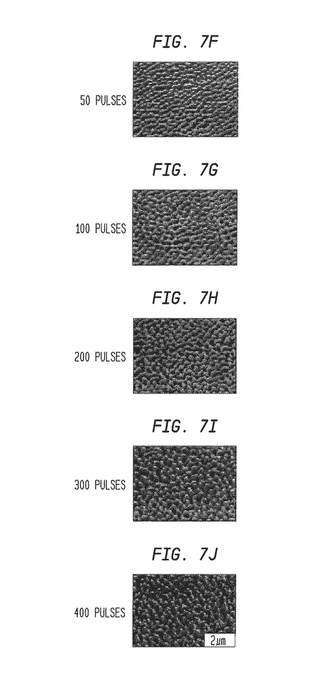
The present invention is directed generally to methods for generating submicron-sized features on a semiconductor surface by irradiating the surface with short laser pulses. The methods allow modulating the sizes of these features by selecting the irradiation wavelength and/or placing a surface portion to be irradiated in contact with a fluid. The invention can provide formation of features that are substantially smaller in size than those generated by previous techniques. The generated features can be, for example, in the form of substantially columnar spikes, each of which extends from a base to a tip, that protrude above the surface. In many embodiments, the average height of the spikes (i.e., the average separation between the base and the tip) can be less than about 1 micron, and the spikes can have an average width--defined, for example, as the average of the largest dimensions of cross-sections of the spikes at half way between the base and the tip--that ranges from, about 100 nm to about 500 nm (e.g., in a range of about 100 nm to about 300 nm).
In one aspect, the present invention provides a method of processing a semiconductor substrate that includes placing at least a portion of a surface of the substrate in contact with a fluid, and exposing that portion to one or more short laser pulses so as to modify its topography. The laser pulses can be selected to have pulse widths in a range of about 50 femtoseconds to about a few nanoseconds, and more preferably in a range of about 100 femtoseconds to about 500 femtoseconds.
In a related aspect, the laser pulses are selected to have energies in a range of about 10 microjoules to about 400 microjoules (e.g., 60 microjoules), and fluences in a range about 1 kJ/m.sup.2 to about 30 kJ/m.sup.2, or from about 3 kJ/m.sup.2 to about 15 kJ/m.sup.2, or from about 3 to about 8 kJ/m.sup.2. The central wavelength of the pulses can be selected to be less than about 800 nm, and preferably in a range of about 400 nm to less than about 800 nm. The number of pulses applied to each location of the surface can be, e.g., in a range of about 1 to about 2500.
In many embodiments, utilizing irradiation wavelengths that are less than about 800 nm, e.g., 400 nm, and/or placing the irradiated portion in contact with the liquid (e.g., water) can lead to formation of sub-micron-sized features over the substrate's surface.
In further aspects, in the above method, the fluid can be selected to be any suitable polar or non-polar liquid. Some examples of such liquids include, without limitation, water, alcohol and silicon oil. Further, the semiconductor substrate can be selected to suit a particular application. By way of example, in some embodiments, the substrate can be an undoped or doped silicon wafer (e.g., an n-doped silicon wafer).
In another aspect, the invention provides a semiconductor substrate that includes a surface layer having at least a portion that exhibits an undulating topography characterized by a plurality of submicron-sized features having an average height less than about 1 micrometer and an average width in a range of about 100 nm to about 500 nm, and preferably in a range of about 100 nm to about 300 nm. The substrate can be any suitable semiconductor substrate, e.g., silicon.
In related aspects, the surface layer has a thickness in a range of about 100 nm to about 1 micrometer and the submicron-sized features comprise spikes each of which extends from a base to tip separated from the base by a distance that is less than about 1 micron. For example, the spikes can protrude above the semiconductor surface by a distance in a range of about 100 nm to about 300 nm.
In another aspect, a method of processing a silicon substrate is disclosed that includes irradiating a portion of a semiconductor surface with one or more femto-second laser pulses having a center wavelength in a range of about 400 nm to less than about 800 nm so as to generate a plurality of submicron-sized spikes within an upper layer of that surface. The spikes can have an average height less than about 1 micrometer and an average width in a range of about 100 nm to about 590 nm.
In a related aspect, in the above method, the irradiation of the surface portion is performed while that portion is in contact with a fluid. By way of example, the fluid can include a polar or non-polar liquid, or a gas, e.g., one having an electron-donating constituent.
In a related aspect, the above method further calls for disposing a solid substance having an electron-donating constituent on the surface portion that is in contact with the fluid prior to its irradiation by the laser pulses. For example, sulfur powder can be applied to the surface followed by disposing a layer of fluid (e.g., having a thickness in a range of about 1 mm to about 20 mm) on the surface. Subsequently, the surface can be irradiated by the laser pulses so as to generate the spikes within an upper layer of the surface and also generate sulfur inclusions in that layer.
In another aspect, the fluid that is in contact with the substrate's surface comprises an aqueous solution, e.g., one containing an electron-donating constituent. By way of example, the liquid can comprise sulfuric acid.
In a further aspect, a method of processing a semiconductor substrate is disclosed that includes disposing a solid substance having an electron-donating constituent on at least a portion of a surface of the substrate, and irradiating that surface portion with one or more pulses having pulse widths in a range of about 50 fs to about 500 fs so as to generate a plurality of inclusions containing the electron-donating constituent in a surface layer of the substrate. The electron-donating constituent can be, for example, a sulfur-containing substance.
Further understanding of various aspects of the invention can be obtained by reference to the following detailed description in conjunction with the associated drawings, which are described briefly below.
BRIEF DESCRIPTION OF THE DRAWINGS
FIG. 1 is a flow chart depicting various steps in one exemplary embodiment of a method according to the teachings of the invention.
FIG. 2 schematically depicts a semiconductor substrate on a surface of which a plurality of submicron-sized spikes are formed in accordance with the teachings of the invention,
FIG. 3 is a flow chart depicting steps in another exemplary embodiment of a method according to the teachings of the invention for changing topography of a semiconductor surface,
FIG. 4 is a schematic diagram of an exemplary apparatus suitable for use in practicing the processing methods of the invention,
FIGS. 5A and 5B are scanning electron micrographs of silicon spikes formed on a silicon surface viewed at 45.degree. angle relative to a normal to the surface, formed by placing the surface in contact with distilled water and irradiating it with 100-fs, 400-nm, 60-.mu.J laser pulses,
FIG. 5C is a scanning electron micrograph of the spikes shown in FIGS. 5A-5B viewed from the side,
FIG. 6A is another scanning electron micrograph of silicon spikes formed in distilled water by irradiating a silicon surface with femtosecond pulses before etching the surface to remove an upper silicon oxide layer,
FIG. 6B is a scanning electron micrograph of the silicon spikes of FIG. 6A after having been subjected to etching in HF, and
FIGS. 7A-7J are scanning electron micrographs of a silicon surface irradiated while in contact with distilled water by an increasing number of laser pulses (the width of the irradiated area is approximately 50 .mu.m).
DETAILED DESCRIPTION
The present invention generally provides semiconductor substrates having surfaces that exhibit submicron-sized structures, and methods for generating such structures. In many embodiments, the submicron-sized structures are generated by irradiating a semiconductor substrate's surface with ultra short laser pulses (e.g. femtosecond pulses) while maintaining the surface in contact with a fluid (e.g., water). Exemplary embodiments of the invention are discussed below.
With reference to a flow chart 10 of FIG. 1, in one exemplar embodiment of a method according to the teachings of the invention for processing a semiconductor substrate, in a step 12, at least a portion of the substrate surface is placed in contact with a fluid, for example, by disposing a layer of the fluid over that portion. In another step 14, the substrate portion that is in contact with the fluid is exposed to one or more short laser pulses so as to modify its surface topography. The laser pulses can have pulse widths in a range of about 100 fs to about a few ns, and more preferably in a range of about 100 fs to about 500 fs. In this exemplary embodiment, the center wavelength of the pulses is chosen to be about 400 nm. More generally, wavelengths in a range of about 400 nm to less than about 800 nm can be employed. The pulse energies can be in a range of about 10 microjoules to about 400 microjoules, and preferably in a range of about 60 microjoules to about 100 microjoules.
The modification of the surface topography can include generating submicron-sized features in an upper surface layer of the substrate. For example, the submicron-sized features can include a plurality of microstructured spikes, e.g., columnar structures extending from the surface to a height above the surface. FIG. 2 schematically depicts a plurality of such features (also referred to herein as spikes) 16 formed on a semiconductor substrate surface 18. Each spike can be characterized by a height and a width (the spikes are shown only for illustrative purposes and are not intended to indicate actual density, size or shape). For example, a spike 16a has a height H defined as the separation between its base 20 and its tip 22, and a width defined by a diameter D of a cross-section, e.g., one substantially parallel to the substrate surface, at a location half way between the base and the tip. In ease of irregularly shaped spikes, the width can correspond, e.g., to the largest linear dimension of such a cross-section of the spike. In many embodiments, the submicron-sized features exhibit an average height of about 1 micrometer (e.g., a height in a range of about 200 nm about 1 micrometer) and an average width in a range of about 100 nm to about 500 nm, or in a range of about 100 nm to about 300 nm.
In general, the fluid is selected to be substantially transparent to radiation having wavelength components in a range of about 400 nm to about 800 nm. Further, the thickness of the fluid layer is preferably chosen so as to ensure that it would not interfere with the laser pulses (e.g., via excessive self-focusing of the pulses) in a manner that would inhibit irradiation of the substrate surface. While in this embodiment water is selected as the fluid, in other embodiments other fluids, such as alcohol or silicon oil, can be employed.
In some embodiments, at least a portion of the substrate can be placed in contact with an aqueous solution having an electron-donating constituent. For example, a solution of sulfuric acid can be applied to at least a portion of the substrate followed by irradiating that portion with short pulses (e.g., femto-second pulses) to not only cause a change in surface topography in a manner described above but also generate sulfur inclusions within a surface layer of the substrate.
Referring to a flow chart 24 of FIG. 3, in another embodiment, initially a solid compound, e.g., sulfur powder, is applied to at least a portion of a semiconductor substrate surface (e.g., a surface of a silicon wafer) (step 26). Subsequently, in a step 28, that surface portion is placed in contact with a fluid (e.g., water) and is irradiated (step 30) by one or more short laser pulses (e.g., pulses with pulse widths in a range of about 100 fs to about a few ns, and preferably in a range of about 100 fs to about 500 fs) so as to cause a change in topography of that portion. Similar to the previous embodiment, the pulse energies can be chosen to be in a range of about 10 microjoules to about 400 microjoules (e.g., 10-150 microjoules).
FIG. 4 schematically depicts an exemplary apparatus 32 suitable for performing the above methods of processing a semiconductor substrate. The apparatus 32 includes a Titanium-Sapphire (Ti:Sapphire) laser 34 that generates laser pulses with a pulse width of 80 femtoseconds at 800 mm wavelength having an average power of 300 mW and at a repetition rate of 95 MHz. The pulses generated by the Ti:Sapphire laser are applied to a chirped-pulse regenerative amplifier 36 that, in turn, produces 0.4 millijoule (mJ), 100 femtosecond pulses at a wavelength of 800 nm and at a repetition rate of 1 kilohertz.
The apparatus 32 further includes a harmonic generation system 38 that receives the amplified pulses and doubles their frequency to produce 140 microjoule, 100-femtosecond second-harmonic pulses at a wavelength of 400 nanometers. The harmonic generation system can be of the type commonly utilized in the art. For example, it can include a lens 38a for focusing the incoming pulses into a doubling crystal 38b to cause a portion of the incoming radiation to be converted into second-harmonic pulses. A dichroic mirror 38c can direct the second-harmonic pulses to a lens 40, and a beam stop 38d can absorb the portion of the radiation that remains at the fundamental frequency.
The lens 40 focuses the second-harmonic pulses onto a surface of a sample 42 (e.g., a silicon wafer) disposed on a 3-dimensional translation system 44 within a vacuum chamber 46. A glass liquid cell 48 is coupled to the stage over the sample so as to allow a sample surface to have contact with the fluid (e.g., water) contained within the cell. The three-dimensional stage allows moving the sample relative to the laser pulses for exposing different portions of the surface to radiation. The vacuum chamber can be utilized to pump out air bubbles in the fluid. Alternatively, the processing of the sample can be performed without utilizing a vacuum chamber.
To Illustrate the efficacy of the teachings of the invention and only for illustrative purposes, submicrometer-sized silicon spikes were generated in surface layers of silicon wafers submerged in water by irradiating those surfaces with 400-nm, 100-fs laser pulses. For example, a Si (111) wafer was initially cleaned with acetone and rinsed in methanol. The wafer was placed in a glass container, such as the container 48 described above, that was filled with distilled water and mounted on a three-axis stage. The silicon surface in contact with the water was irradiated by a 1-KHz train of 100-fs, 60-microjoule pulses at a central wavelength of 400 nm generated by a frequency-doubled, amplified Ti:Sapphire laser, such as that described above. A fast shutter was utilized to control the number of laser pulses incident on the silicon surface. The laser pulses were focused by a 0.25-m focal-length lens to a focal point about 10 mm behind the silicon surface. The pulses traveled through about 10 mm of water before striking the silicon surface at normal incidence. The spatial profile of the laser spot at the sample surface was nearly Gaussian characterized by a fixed beam waist of about 50 microns. To correct for chirping of the laser pulses in the water and to ensure minimum pulse duration at the silicon surface, the pulses were pre-chirped to obtain the lowest possible damage threshold at that surface. The results, however, did not depend strongly on the chirping of the laser pulses.
During sample irradiation, the irradiated sample surface was monitored with an optical imaging system having a spatial resolution of about 5 microns. It was observed that irradiation cause formation of micrometer-sized water bubbles at the silicon-water interface. After a single pulse, two or three microbubbles were generated; after irradiation with trains of laser pulses thousands of bubbles were generated. It was also observed that some bubbles at times would coalesce to form larger ones, which would adhere to the silicon surface. These larger bubbles were removed by shaking the cell.
FIGS. 5A, 5B, and 5C present electron micrographs of the silicon surface after irradiation with one thousand laser pulses, showing formation of a plurality of spikes on the surface. The spikes have a substantially columnar shape with a typical height of about 500 nm and a typical diameter of about 200 nm. They protrude up to about 100 nm above the original surface of the wafer (FIG. 1C). The shape of the spikes is more columnar than the conical spikes that can be formed in the presence of SF.sub.6 as disclosed in the above-referenced patent applications.
The chemical composition of the uppermost 10 nm of the silicon surface layer having the spikes was determined by employing X-ray photoelectron spectroscopy (XPS). The XPS spectra showed that this layer is composed of about 83% SiO.sub.2 and about 17% silicon. The wafer was etched in 5% HF for about 15 minutes to remove the SiO.sub.2 layer (about 20 nm in thickness) while leaving the underlying unoxidized Si intact. A comparison of the electron micrographs of the spikes before etching (FIG. 6A) with those obtained after etching (FIG. 6B) showed that the etching process had reduced the width of the spikes by about 40 nm and had rendered their surfaces smoother. After etching, no SiO.sub.2 was detected in the X-ray photoelectron spectra of the sample, thereby indicating that the interior of the spikes consisted of silicon and that the spikes were covered prior to etching by an oxide layer that was at most about 20 nm thick.
To study the development of the spikes, silicon samples were irradiated, with different numbers of laser pulses. FIG. 7A-7J show a series of scanning electron micrographs of the surface of a silicon substrate irradiated with an increasing number of femtosecond laser pulses while in contact with water, in a manner described above. The images only show the central portion of the irradiated area. As shown in FIG. 7A, a single laser pulse forms surface structures resembling ripples on a liquid surface with a wavelength of about 500 nm. Lower magnification micrographs (not shown here) indicate that the irradiated region typically contains two or three of these ripple-like structures. Without being limited to any particular theory, each ripple structure is likely to correspond to one of the microbubbles that were observed after irradiation.
Referring to FIG. 7B, after two pulses, the surface shows overlapping ripple structures. As the number of laser pulses is increased from 5 to 20 (FIGS. 7C, 7D and 7E), the silicon surface roughens from the interaction of many ripple structures. After exposure to 50 laser pulses (FIG. 7F), the surface is covered with submicrometer bead-like structures, which then evolve into spikes as the number of pulses is further increased as shown in FIGS. 7G, 7H, 7I and 7J corresponding, respectively, to irradiating the surface with 100, 200, 300 and 400 laser pulses. The average separation of the resulting spikes is roughly 500 nm and substantially equal to the wavelength of the initial ripple structures.
The above silicon spikes prepared in water are one to two orders of magnitude smaller than spikes that can be generated in a silicon substrate exposed to laser pulses in presence of a gas, such as those described in the above-referenced copending patent applications. This remarkable size difference suggests different formation mechanisms for the two types of spikes.
Without being limited to any particular theory, it is noted that when a 400-nm laser pulse interacts with the silicon surface, most of the light is absorbed by a silicon layer tens of nanometers thick near the silicon-water interface. The absorption of intense light in such a thin silicon layer can excite a plasma at the silicon-water interface, which can then equilibrate with the surrounding water and silicon, leaving behind a molten silicon layer on the surface. The molten layer can solidify before the next laser pulse arrives. Due to the high temperature of the plasma, some of the water can vaporize or dissociate, thereby generating bubbles at the silicon-water interface. The large bubbles that were observed after irradiation in the above experiments remain in the water for days, thus suggesting that they consist primarily of gaseous hydrogen and oxygen rather than water vapor.
Again, without being limited to any particular theory, several possible mechanisms can be considered by which the bubbles may produce the wave-like structures shown in FIGS. 7A-7G. Diffraction of the laser beam by the bubbles may produce rings of light intensity on the silicon surface, or the heat of vaporization and dissociation required to form a bubble at the silicon-water interface may cool the silicon surface locally, exciting a capillary wave in the molten silicon through Marangoni flow. The latter is the most likely formation mechanism for the structures observed after a single pulse; those structures cannot be formed by diffraction from a laser-induced bubble, as the pulse duration is only 100 fs, and the observed wave-like structures can be several micrometers in diameter. A micrometer-sized bubble requires much longer than 100 fs to form and therefore cannot diffract the first pulse.
Roughness on the silicon surface can cause an uneven absorption of the laser pulse energy across the surface. The resulting non-uniform temperature of the surface can produce a random arrangement of bubbles. Silicon-water has a contact angle more than 45.degree. making a gaseous layer between the silicon and water unstable and leading to the formation of bubbles. The vaporization and dissociation of the bubbles can remove thermal energy from the molten silicon surface just below the bubbles, causing the surface to cool rapidly. Because the surface tension of liquid silicon decreases with increasing temperature, the surrounding hot liquid silicon flows toward the cooled region, deforming the surface. This deformation can then excite a circular capillary wave at the liquid-silicon surface. Superposition of ripple-structures caused by multiple laser pulses can then produce the randomly distributed submicrometer beads that appear after 20 laser pulses (See FIGS. 7F-7J). These beads subsequently sharpen into spikes through preferential removal of material around the beads by laser-assisted etching.
As noted above, the morphology and sizes of the above spikes generated in a silicon surface by exposing it to femtosecond laser pulses while in contact with water can be different than those observed for spikes generated by irradiating a silicon surface with femtosecond pulses in presence of a gas, such as SF.sub.6. The early stage of submicrometer spike formation in water can be different from that in gaseous SF.sub.6, while the later stages can be similar. In SF.sub.6, straight submicrometer-sized ripple structures first form on the silicon surface, then coarser, micrometer-scale ridges form on top of (and perpendicular to) the ripples. Next, the coarsened layer breaks up into micrometer-sized beads, and finally the beads evolve into spikes through etching. In both SF.sub.6 and water, the length scale of the final structures is set by the arrangement of beadlike structures that form after roughly 10-20 pulses, and this length scale appears to be determined by capillary waves in the molten silicon. The much smaller size of the spikes formed in water is likely to be due to a difference in capillary wavelength in the two cases.
The molten silicon layer is expected to solidify much faster in water than in SF.sub.6, as the thermal conductivity and heat capacity of liquid water are much greater than those of gaseous SF.sub.6. The dispersion relation for capillary waves in a shallow layer of molten silicon indicates that decreasing the lifetime of the molten layer should also decrease the longest allowed capillary wavelength. Using a simple model that neglects the effects of ablation and cooling by heat transfer to the environment to calculate the lifetime and depth of the liquid layer, it was found that the longest allowed capillary wavelength is about 1 micron. Because the lifetime is certainly reduced by the flow of heat to the surrounding water in the experiments presented above, the longest allowed wavelength should be less than 1 micron, which is in agreement with submicrometer spike separation observed here.
In some embodiments, rather than utilizing a fluid, a solid substance having an electron-donating constituent (e.g., a sulfur powder) is disposed on at least a portion of a surface of semiconductor substrate, e.g., a silicon wafer. That surface portion is then irradiated with one or more pulses having pulse widths in a range of about 50 fs to about 500 fs so as to generate a plurality of inclusions containing the electron donating constituent in a surface layer of the substrate.
Those having ordinary skill in the art will appreciate that various changes can be made to the above embodiments without departing from the scope of the invention.
* * * * *
References
D00000
D00001
D00002
D00003
D00004
D00005
D00006
D00007
XML
uspto.report is an independent third-party trademark research tool that is not affiliated, endorsed, or sponsored by the United States Patent and Trademark Office (USPTO) or any other governmental organization. The information provided by uspto.report is based on publicly available data at the time of writing and is intended for informational purposes only.
While we strive to provide accurate and up-to-date information, we do not guarantee the accuracy, completeness, reliability, or suitability of the information displayed on this site. The use of this site is at your own risk. Any reliance you place on such information is therefore strictly at your own risk.
All official trademark data, including owner information, should be verified by visiting the official USPTO website at www.uspto.gov. This site is not intended to replace professional legal advice and should not be used as a substitute for consulting with a legal professional who is knowledgeable about trademark law.