Vector signaling codes for densely-routed wire groups
Shokrollahi , et al.
U.S. patent number 10,333,741 [Application Number 15/499,866] was granted by the patent office on 2019-06-25 for vector signaling codes for densely-routed wire groups. This patent grant is currently assigned to KANDOU LABS, S.A.. The grantee listed for this patent is Kandou Labs, S.A.. Invention is credited to Ali Hormati, Amin Shokrollahi, Armin Tajalli.


View All Diagrams
| United States Patent | 10,333,741 |
| Shokrollahi , et al. | June 25, 2019 |
Vector signaling codes for densely-routed wire groups
Abstract
Methods and systems are described for receiving signal elements corresponding to a first group of symbols of a vector signaling codeword over a first densely-routed wire group of a multi-wire bus at a first set of multi-input comparators (MICs), receiving signal elements corresponding to a second group of symbols of the vector signaling codeword over a second densely-routed wire group of the multi-wire bus at a second set of MICs, and receiving signal elements corresponding to the first and the second groups of symbols of the vector signaling codeword at a global MIC.
| Inventors: | Shokrollahi; Amin (Preverenges, CH), Hormati; Ali (Ecublens Vaud, CH), Tajalli; Armin (Chavannes pres Renens, CH) | ||||||||||
|---|---|---|---|---|---|---|---|---|---|---|---|
| Applicant: |
|
||||||||||
| Assignee: | KANDOU LABS, S.A. (Lausanne,
CH) |
||||||||||
| Family ID: | 60158706 | ||||||||||
| Appl. No.: | 15/499,866 | ||||||||||
| Filed: | April 27, 2017 |
Prior Publication Data
| Document Identifier | Publication Date | |
|---|---|---|
| US 20170317855 A1 | Nov 2, 2017 | |
Related U.S. Patent Documents
| Application Number | Filing Date | Patent Number | Issue Date | ||
|---|---|---|---|---|---|
| 62328721 | Apr 28, 2016 | ||||
| Current U.S. Class: | 1/1 |
| Current CPC Class: | H04L 25/0276 (20130101); H04L 25/4919 (20130101); H04L 25/0292 (20130101); H04L 25/03343 (20130101); H04L 25/0272 (20130101) |
| Current International Class: | H04L 25/49 (20060101); H04L 25/03 (20060101); H04L 25/02 (20060101) |
| Field of Search: | ;341/50,58,68-70 ;375/242-254,259-285,286-288 |
References Cited [Referenced By]
U.S. Patent Documents
| 668687 | February 1901 | Mayer |
| 780883 | January 1905 | Hinchman |
| 3196351 | July 1965 | Slepian |
| 3636463 | January 1972 | Ongkiehong |
| 3939468 | February 1976 | Mastin |
| 4163258 | July 1979 | Ebihara |
| 4181967 | January 1980 | Nash |
| 4206316 | June 1980 | Burnsweig |
| 4276543 | June 1981 | Miller |
| 4486739 | December 1984 | Franaszek |
| 4499550 | February 1985 | Ray, III |
| 4722084 | January 1988 | Morton |
| 4772845 | September 1988 | Scott |
| 4774498 | September 1988 | Traa |
| 4864303 | September 1989 | Ofek |
| 4897657 | January 1990 | Brubaker |
| 4974211 | November 1990 | Corl |
| 5017924 | May 1991 | Guiberteau |
| 5053974 | October 1991 | Penz |
| 5166956 | November 1992 | Baltus |
| 5168509 | December 1992 | Nakamura |
| 5266907 | November 1993 | Dacus |
| 5283761 | February 1994 | Gillingham |
| 5287305 | February 1994 | Yoshida |
| 5311516 | May 1994 | Kuznicki |
| 5331320 | July 1994 | Cideciyan |
| 5334956 | August 1994 | Leding et al. |
| 5412689 | May 1995 | Chan |
| 5449895 | September 1995 | Hecht |
| 5459465 | October 1995 | Kagey |
| 5461379 | October 1995 | Weinman |
| 5510736 | April 1996 | Van De Plassche |
| 5511119 | April 1996 | Lechleider |
| 5553097 | September 1996 | Dagher |
| 5566193 | October 1996 | Cloonan |
| 5599550 | February 1997 | Kohlruss |
| 5626651 | May 1997 | Dullien |
| 5629651 | May 1997 | Mizuno |
| 5659353 | August 1997 | Kostreski |
| 5727006 | March 1998 | Dreyer |
| 5748948 | May 1998 | Yu |
| 5802356 | September 1998 | Gaskins |
| 5825808 | October 1998 | Hershey |
| 5856935 | January 1999 | Moy |
| 5875202 | February 1999 | Venters |
| 5945935 | August 1999 | Kusumoto |
| 5949060 | September 1999 | Schattschneider |
| 5982954 | November 1999 | Delen |
| 5995016 | November 1999 | Perino |
| 5999016 | December 1999 | McClintock |
| 6005895 | December 1999 | Perino |
| 6084883 | July 2000 | Norrell |
| 6119263 | September 2000 | Mowbray |
| 6154498 | November 2000 | Dabral |
| 6172634 | January 2001 | Leonowich |
| 6175230 | January 2001 | Hamblin |
| 6232908 | May 2001 | Nakaigawa |
| 6278740 | August 2001 | Nordyke |
| 6316987 | November 2001 | Dally |
| 6317465 | November 2001 | Akamatsu |
| 6346907 | February 2002 | Dacy |
| 6359931 | March 2002 | Perino |
| 6378073 | April 2002 | Davis |
| 6384758 | May 2002 | Michalski |
| 6396329 | May 2002 | Zerbe |
| 6398359 | June 2002 | Silverbrook |
| 6400302 | June 2002 | Amazeen |
| 6404820 | June 2002 | Postol |
| 6417737 | July 2002 | Moloudi |
| 6433800 | August 2002 | Holtz |
| 6452420 | September 2002 | Wong |
| 6473877 | October 2002 | Debendra Das |
| 6483828 | November 2002 | Balachandran |
| 6504875 | January 2003 | Perino |
| 6509773 | January 2003 | Buchwald |
| 6522699 | February 2003 | Anderson |
| 6556628 | April 2003 | Poulton |
| 6563382 | May 2003 | Yang |
| 6621427 | September 2003 | Greenstreet |
| 6624699 | September 2003 | Yin |
| 6650638 | November 2003 | Walker |
| 6661355 | December 2003 | Cornelius |
| 6664355 | December 2003 | Kim |
| 6686879 | February 2004 | Shattil |
| 6690739 | February 2004 | Mui |
| 6766342 | July 2004 | Kechriotis |
| 6772351 | August 2004 | Werner |
| 6839429 | January 2005 | Gaikwad |
| 6839587 | January 2005 | Yonce |
| 6854030 | February 2005 | Perino |
| 6865234 | March 2005 | Agazzi |
| 6865236 | March 2005 | Terry |
| 6876317 | April 2005 | Sankaran |
| 6898724 | May 2005 | Chang |
| 6927709 | August 2005 | Kiehl |
| 6954492 | October 2005 | Williams |
| 6963622 | November 2005 | Eroz |
| 6972701 | December 2005 | Jansson |
| 6973613 | December 2005 | Cypher |
| 6976194 | December 2005 | Cypher |
| 6982954 | January 2006 | Dhong |
| 6990138 | January 2006 | Bejjani |
| 6991038 | January 2006 | Guesnon |
| 6993311 | January 2006 | Li |
| 6999516 | February 2006 | Rajan |
| 7023817 | April 2006 | Kuffner |
| 7039136 | May 2006 | Olson |
| 7053802 | May 2006 | Cornelius |
| 7075996 | July 2006 | Simon |
| 7080288 | July 2006 | Ferraiolo |
| 7082557 | July 2006 | Schauer |
| 7085153 | August 2006 | Ferrant |
| 7085336 | August 2006 | Lee |
| 7123660 | October 2006 | Haq |
| 7127003 | October 2006 | Rajan |
| 7130944 | October 2006 | Perino |
| 7142612 | November 2006 | Horowitz |
| 7142865 | November 2006 | Tsai |
| 7145411 | December 2006 | Blair |
| 7164631 | January 2007 | Tateishi |
| 7167019 | January 2007 | Broyde |
| 7176823 | February 2007 | Zabroda |
| 7180949 | February 2007 | Kleveland |
| 7184483 | February 2007 | Rajan |
| 7188199 | March 2007 | Leung |
| 7199728 | April 2007 | Dally |
| 7231558 | June 2007 | Gentieu |
| 7269130 | September 2007 | Pitio |
| 7269212 | September 2007 | Chau |
| 7335976 | February 2008 | Chen |
| 7336112 | February 2008 | Sha |
| 7336139 | February 2008 | Blair |
| 7339990 | March 2008 | Hidaka |
| 7346819 | March 2008 | Bansal |
| 7348989 | March 2008 | Stevens |
| 7349484 | March 2008 | Stojanovic |
| 7356213 | April 2008 | Cunningham |
| 7358869 | April 2008 | Chiarulli |
| 7362130 | April 2008 | Broyde |
| 7362697 | April 2008 | Becker |
| 7366942 | April 2008 | Lee |
| 7370264 | May 2008 | Worley |
| 7372390 | May 2008 | Yamada |
| 7389333 | June 2008 | Moore |
| 7397302 | July 2008 | Bardsley |
| 7400276 | July 2008 | Sotiriadis |
| 7428273 | September 2008 | Foster |
| 7456778 | November 2008 | Werner |
| 7462956 | December 2008 | Lan |
| 7496162 | February 2009 | Srebranig |
| 7570704 | April 2009 | Nagarajan |
| 7535957 | May 2009 | Ozawa |
| 7539532 | May 2009 | Tran |
| 7599390 | October 2009 | Pamarti |
| 7613234 | November 2009 | Raghavan |
| 7616075 | November 2009 | Kushiyama |
| 7620116 | November 2009 | Bessios |
| 7626442 | December 2009 | Zerbe |
| 7633850 | December 2009 | Nagarajan |
| 7639596 | December 2009 | Cioffi |
| 7643588 | January 2010 | Visalli |
| 7650525 | January 2010 | Chang |
| 7656321 | February 2010 | Wang |
| 7688929 | March 2010 | Co |
| 7694204 | April 2010 | Schmidt |
| 7697915 | April 2010 | Behzad |
| 7698088 | April 2010 | Sul |
| 7706456 | April 2010 | Laroia |
| 7706524 | April 2010 | Zerbe |
| 7746764 | June 2010 | Rawlins |
| 7768312 | August 2010 | Hirose |
| 7787572 | August 2010 | Scharf |
| 7804361 | September 2010 | Lim |
| 7808456 | October 2010 | Chen |
| 7808883 | October 2010 | Green |
| 7826551 | November 2010 | Lee |
| 7841909 | November 2010 | Murray |
| 7859356 | December 2010 | Pandey |
| 7868790 | January 2011 | Bae |
| 7869497 | January 2011 | Benvenuto |
| 7869546 | January 2011 | Tsai |
| 7882413 | February 2011 | Chen |
| 7899653 | March 2011 | Hollis |
| 7907676 | March 2011 | Stojanovic |
| 7933770 | April 2011 | Kruger |
| 7957472 | June 2011 | Wu |
| 8000664 | August 2011 | Khorram |
| 8030999 | October 2011 | Chatterjee |
| 8036300 | October 2011 | Evans |
| 8050332 | November 2011 | Chung |
| 8055095 | November 2011 | Palotai |
| 8064535 | November 2011 | Wiley |
| 8085172 | December 2011 | Li |
| 8091006 | January 2012 | Prasad |
| 8106806 | January 2012 | Toyomura |
| 8149906 | April 2012 | Saito |
| 8159375 | April 2012 | Abbasfar |
| 8159376 | April 2012 | Abbasfar |
| 8180931 | May 2012 | Lee |
| 8185807 | May 2012 | Oh |
| 8199849 | June 2012 | Oh |
| 8199863 | June 2012 | Chen |
| 8218670 | July 2012 | AbouRjeily |
| 8233544 | July 2012 | Bao |
| 8245094 | August 2012 | Jiang |
| 8253454 | August 2012 | Lin |
| 8274311 | September 2012 | Liu |
| 8279094 | October 2012 | Abbasfar |
| 8279745 | October 2012 | Dent |
| 8279976 | October 2012 | Lin |
| 8284848 | October 2012 | Nam |
| 8289914 | October 2012 | Li |
| 8295250 | October 2012 | Gorokhov |
| 8295336 | October 2012 | Lutz |
| 8305247 | November 2012 | Pun |
| 8310389 | November 2012 | Chui |
| 8341492 | December 2012 | Shen |
| 8359445 | January 2013 | Ware |
| 8365035 | January 2013 | Hara |
| 8406315 | March 2013 | Tsai |
| 8406316 | March 2013 | Sugita |
| 8429492 | April 2013 | Yoon |
| 8429495 | April 2013 | Przybylski |
| 8437440 | May 2013 | Zhang |
| 8442099 | May 2013 | Sederat |
| 8442210 | May 2013 | Zerbe |
| 8443223 | May 2013 | Abbasfar |
| 8451913 | May 2013 | Oh |
| 8462891 | June 2013 | Kizer |
| 8472513 | June 2013 | Malipatil |
| 8620166 | June 2013 | Dong |
| 8498344 | July 2013 | Wilson |
| 8498368 | July 2013 | Husted |
| 8520348 | August 2013 | Dong |
| 8520493 | August 2013 | Goulahsen |
| 8539318 | September 2013 | Cronie |
| 8547272 | October 2013 | Nestler |
| 8577284 | November 2013 | Seo |
| 8578246 | November 2013 | Mittelholzer |
| 8588254 | November 2013 | Diab |
| 8588280 | November 2013 | Oh |
| 8593305 | November 2013 | Tajalli |
| 8602643 | December 2013 | Gardiner |
| 8604879 | December 2013 | Mourant |
| 8638241 | January 2014 | Sudhakaran |
| 8643437 | February 2014 | Chiu |
| 8649445 | February 2014 | Cronie |
| 8649460 | February 2014 | Ware |
| 8649556 | February 2014 | Wedge |
| 8649840 | February 2014 | Sheppard, Jr. |
| 8674861 | March 2014 | Matsuno |
| 8687968 | April 2014 | Nosaka |
| 8711919 | April 2014 | Kumar |
| 8718184 | May 2014 | Cronie |
| 8755426 | June 2014 | Cronie |
| 8773964 | July 2014 | Hsueh |
| 8780687 | July 2014 | Clausen |
| 8782578 | July 2014 | Tell |
| 8791735 | July 2014 | Shibasaki |
| 8831440 | September 2014 | Yu |
| 8841936 | September 2014 | Nakamura |
| 8879660 | November 2014 | Peng |
| 8897134 | November 2014 | Kern |
| 8898504 | November 2014 | Baumgartner |
| 8938171 | January 2015 | Tang |
| 8949693 | February 2015 | Ordentlich |
| 8951072 | February 2015 | Hashim |
| 8975948 | March 2015 | GonzalezDiaz |
| 8989317 | March 2015 | Holden |
| 8996740 | March 2015 | Wiley |
| 9015566 | April 2015 | Cronie |
| 9020049 | April 2015 | Schwager |
| 9036764 | May 2015 | Hossain |
| 9059816 | June 2015 | Simpson |
| 9069995 | June 2015 | Cronie |
| 9077386 | July 2015 | Holden |
| 9083576 | July 2015 | Hormati |
| 9093791 | July 2015 | Liang |
| 9100232 | August 2015 | Hormati |
| 9106465 | August 2015 | Walter |
| 9124557 | September 2015 | Fox |
| 9148087 | September 2015 | Tajalli |
| 9152495 | October 2015 | Losh |
| 9165615 | October 2015 | Amirkhany |
| 9172412 | October 2015 | Kim |
| 9178503 | November 2015 | Hsieh |
| 9183085 | November 2015 | Northcott |
| 9197470 | November 2015 | Okunev |
| 9231790 | January 2016 | Wiley |
| 9246713 | January 2016 | Shokrollahi |
| 9281785 | March 2016 | Sjoland |
| 9288082 | March 2016 | Ulrich |
| 9288089 | March 2016 | Cronie |
| 9292716 | March 2016 | Winoto |
| 9300503 | March 2016 | Holden |
| 9306621 | April 2016 | Zhang |
| 9319218 | April 2016 | Pandey |
| 9331962 | May 2016 | Lida |
| 9362974 | June 2016 | Fox |
| 9363114 | June 2016 | Shokrollahi |
| 9374250 | June 2016 | Musah |
| 9401828 | July 2016 | Cronie |
| 9432082 | August 2016 | Ulrich |
| 9432298 | August 2016 | Smith |
| 9444654 | September 2016 | Hormati |
| 9455744 | September 2016 | George |
| 9455765 | September 2016 | Schumacher |
| 9461862 | October 2016 | Holden |
| 9479369 | October 2016 | Shokrollahi |
| 9509437 | November 2016 | Shokrollahi |
| 9520883 | December 2016 | Shibasaki |
| 9521058 | December 2016 | Pandey |
| 9537644 | January 2017 | Jones |
| 9544015 | January 2017 | Ulrich |
| 9565036 | February 2017 | Zerbe |
| 9596109 | March 2017 | Fox |
| 9634797 | April 2017 | Benammar |
| 9667379 | May 2017 | Cronie |
| 9686106 | June 2017 | Shokrollahi |
| 9825723 | November 2017 | Holden |
| 9852806 | December 2017 | Stauffer |
| 9906358 | February 2018 | Tajalli |
| 9917711 | March 2018 | Ulrich |
| 9985745 | May 2018 | Shokrollahi |
| 10003315 | June 2018 | Tajalli |
| 10044452 | August 2018 | Holden |
| 10055372 | August 2018 | Shokrollahi |
| 2001/0006538 | July 2001 | Simon |
| 2001/0055344 | December 2001 | Lee |
| 2002/0034191 | March 2002 | Shattil |
| 2002/0044316 | April 2002 | Myers |
| 2002/0057592 | May 2002 | Robb |
| 2002/0152340 | October 2002 | Dreps |
| 2002/0154633 | October 2002 | Shin |
| 2002/0163881 | November 2002 | Dhong |
| 2002/0167339 | November 2002 | Chang |
| 2002/0174373 | November 2002 | Chang |
| 2002/0181607 | December 2002 | Izumi |
| 2003/0016763 | January 2003 | Doi |
| 2003/0016770 | January 2003 | Trans |
| 2003/0046618 | March 2003 | Collins |
| 2003/0085763 | May 2003 | Schrodinger |
| 2003/0117184 | June 2003 | Fecteau |
| 2003/0146783 | August 2003 | Bandy |
| 2003/0174023 | September 2003 | Miyasita |
| 2003/0185310 | October 2003 | Ketchum |
| 2003/0218558 | November 2003 | Mulder |
| 2004/0027185 | February 2004 | Fiedler |
| 2004/0057525 | March 2004 | Rajan |
| 2004/0146117 | July 2004 | Subramaniam |
| 2004/0155802 | August 2004 | Lamy |
| 2004/0161019 | August 2004 | Raghavan |
| 2004/0169529 | September 2004 | Afghahi |
| 2004/0170231 | September 2004 | Bessios |
| 2004/0239374 | December 2004 | Hori |
| 2005/0063493 | March 2005 | Foster |
| 2005/0134380 | June 2005 | Nairn |
| 2005/0174841 | August 2005 | Ho |
| 2005/0195000 | September 2005 | Parker |
| 2005/0201491 | September 2005 | Wei |
| 2005/0213686 | September 2005 | Love |
| 2005/0220182 | October 2005 | Kuwata |
| 2005/0270098 | December 2005 | Zhang |
| 2006/0013331 | January 2006 | Choi |
| 2006/0036668 | February 2006 | Jaussi |
| 2006/0097786 | May 2006 | Su |
| 2006/0103463 | May 2006 | Lee |
| 2006/0120486 | June 2006 | Visalli |
| 2006/0121801 | June 2006 | Pischl |
| 2006/0126751 | June 2006 | Bessios |
| 2006/0133538 | June 2006 | Stojanovic |
| 2006/0140324 | June 2006 | Casper |
| 2006/0159005 | July 2006 | Rawlins |
| 2006/0232461 | October 2006 | Felder |
| 2006/0233291 | October 2006 | Garlepp |
| 2006/0291589 | December 2006 | Eliezer |
| 2007/0001723 | January 2007 | Lin |
| 2007/0002954 | January 2007 | Cornelius |
| 2007/0009018 | January 2007 | Wang |
| 2007/0030796 | February 2007 | Green |
| 2007/0071113 | March 2007 | Lee |
| 2007/0103338 | May 2007 | Teo |
| 2007/0121716 | May 2007 | Nagarajan |
| 2007/0164883 | July 2007 | Furtner |
| 2007/0182487 | August 2007 | Ozasa |
| 2007/0201546 | August 2007 | Lee |
| 2007/0201597 | August 2007 | He |
| 2007/0204205 | August 2007 | Niu |
| 2007/0263711 | November 2007 | Kramer |
| 2007/0283210 | December 2007 | Prasad |
| 2008/0007367 | January 2008 | Kim |
| 2008/0012598 | January 2008 | Mayer |
| 2008/0104374 | May 2008 | Mohamed |
| 2008/0159448 | July 2008 | Anim-Appiah |
| 2008/0192621 | August 2008 | Suehiro |
| 2008/0317188 | December 2008 | Staszewski |
| 2009/0046009 | February 2009 | Fujii |
| 2009/0059782 | March 2009 | Cole |
| 2009/0115523 | May 2009 | Akizuki |
| 2009/0154604 | June 2009 | Lee |
| 2009/0195281 | August 2009 | Tamura |
| 2009/0262876 | October 2009 | Arima |
| 2009/0316730 | December 2009 | Feng |
| 2009/0323864 | December 2009 | Tired |
| 2010/0046644 | February 2010 | Mazet |
| 2010/0081451 | April 2010 | Mueck |
| 2010/0148819 | June 2010 | Bae |
| 2010/0180143 | July 2010 | Ware |
| 2010/0215087 | August 2010 | Tsai |
| 2010/0215112 | August 2010 | Tsai |
| 2010/0215118 | August 2010 | Ware |
| 2010/0235673 | September 2010 | Abbasfar |
| 2010/0271107 | October 2010 | Tran |
| 2010/0283894 | November 2010 | Horan |
| 2010/0296556 | November 2010 | Rave |
| 2010/0309964 | December 2010 | Oh |
| 2011/0014865 | January 2011 | Seo |
| 2011/0028089 | February 2011 | Komori |
| 2011/0032977 | February 2011 | Hsiao |
| 2011/0051854 | March 2011 | Kizer |
| 2011/0072330 | March 2011 | Kolze |
| 2011/0074488 | March 2011 | Broyde |
| 2011/0084737 | April 2011 | Oh |
| 2011/0103508 | May 2011 | Mu |
| 2011/0127990 | June 2011 | Wilson |
| 2011/0156757 | June 2011 | Hayashi |
| 2011/0228864 | September 2011 | Aryanfar |
| 2011/0235501 | September 2011 | Goulahsen |
| 2011/0268225 | November 2011 | Cronie |
| 2011/0299555 | December 2011 | Cronie |
| 2011/0302478 | December 2011 | Cronie |
| 2011/0317559 | December 2011 | Kern |
| 2012/0082203 | April 2012 | Zerbe |
| 2012/0133438 | May 2012 | Tsuchi |
| 2012/0152901 | June 2012 | Nagorny |
| 2012/0161945 | June 2012 | Single |
| 2012/0213267 | August 2012 | Stojanovic |
| 2012/0213299 | August 2012 | Cronie |
| 2012/0257683 | October 2012 | Schwager |
| 2013/0010892 | January 2013 | Cronie |
| 2013/0013870 | January 2013 | Cronie |
| 2013/0088274 | April 2013 | Gu |
| 2013/0106513 | May 2013 | Cyrusian |
| 2013/0114392 | May 2013 | Sun et al. |
| 2013/0114519 | May 2013 | Gaal |
| 2013/0114663 | May 2013 | Ding |
| 2013/0129019 | May 2013 | Sorrells |
| 2013/0147553 | June 2013 | Iwamoto |
| 2013/0188656 | July 2013 | Ferraiolo |
| 2013/0195155 | August 2013 | Pan |
| 2013/0202065 | August 2013 | Chmelar |
| 2013/0215954 | August 2013 | Beukema |
| 2013/0259113 | October 2013 | Kumar |
| 2013/0271194 | October 2013 | Pellerano |
| 2013/0307614 | November 2013 | Dai |
| 2013/0314142 | November 2013 | Tamura |
| 2013/0315501 | November 2013 | Atanassov |
| 2013/0346830 | December 2013 | Ordentlich |
| 2014/0159769 | June 2014 | Hong |
| 2014/0177645 | June 2014 | Cronie |
| 2014/0177696 | June 2014 | Hwang |
| 2014/0254642 | September 2014 | Fox |
| 2014/0266440 | September 2014 | Itagaki |
| 2014/0269130 | September 2014 | Maeng |
| 2014/0286381 | September 2014 | Shibasaki |
| 2014/0376668 | December 2014 | Shokrollahi |
| 2015/0049798 | February 2015 | Hossein |
| 2015/0070201 | March 2015 | Dedic |
| 2015/0078479 | March 2015 | Whitby-Strevens |
| 2015/0117579 | April 2015 | Shibasaki |
| 2015/0146771 | May 2015 | Walter |
| 2015/0222458 | August 2015 | Hormati |
| 2015/0249559 | September 2015 | Shokrollahi |
| 2015/0333940 | November 2015 | Shokrollahi |
| 2015/0349835 | December 2015 | Fox |
| 2015/0380087 | December 2015 | Mittelholzer |
| 2015/0381232 | December 2015 | Ulrich |
| 2016/0020796 | January 2016 | Hormati |
| 2016/0020824 | January 2016 | Ulrich |
| 2016/0036616 | February 2016 | Holden |
| 2016/0197747 | July 2016 | Ulrich |
| 2016/0211929 | July 2016 | Holden |
| 2016/0218894 | July 2016 | Fox |
| 2016/0261435 | September 2016 | Musah |
| 2016/0294586 | October 2016 | Shokrollahi |
| 2017/0279642 | September 2017 | Fox |
| 2017/0310456 | October 2017 | Tajalli |
| 2017/0317449 | November 2017 | Shokrollahi |
| 2017/0317855 | November 2017 | Shokrollahi |
| 2018/0076912 | March 2018 | Holden |
| 2018/0324008 | November 2018 | Shokrollahi |
| 2018/0351670 | December 2018 | Holden |
| 1864346 | Nov 2006 | CN | |||
| 101478286 | Jul 2009 | CN | |||
| 1926267 | May 2008 | EP | |||
| 2039221 | Feb 2013 | EP | |||
| 2003163612 | Jun 2003 | JP | |||
| 2005002162 | Jan 2005 | WO | |||
| 2009084121 | Jul 2009 | WO | |||
| 2010031824 | Mar 2010 | WO | |||
| 2011119359 | Sep 2011 | WO | |||
Other References
|
Giovaneli, et al., "Space-frequency coded OFDM system for multi-wire power line communications", Power Line Communications and Its Applications, 20015 International Symposium on Vancouver, BC, Canada, Apr. 6-8, 2005, Piscataway, NJ, pp. 191-195. cited by applicant . Shibasaki, et al., "A 56-Gb/s Receiver Front-End with a CTLE and 1-Tap DFE in 20-nm CMOS", IEEE 2014 Symposium on VLSI Circuits Digest of Technical Papers, 2 pgs. cited by applicant . Hidaka, et al., "A 4-Channel 1.25-10.3 Gb/s Backplane Transceiver Macro With35 dB Equalizer and Sign-Based Zero-Forcing Adaptive Control", IEEE Journal of Solid-State Circuits, vol. 44 No. 12, Dec. 2009, pp. 3547-3559. cited by applicant . "Introduction to: Analog Computers and the DSPACE System," Course Material ECE 5230 Spring 2008, Utah State University, www.coursehero.com, 12 pages. cited by applicant . Abbasfar, A., "Generalized Differential Vector Signaling", IEEE International Conference on Communications, ICC 09, (Jun. 14, 2009), pp. 1-5. cited by applicant . Brown, L., et al., "V.92: The Last Dial-Up Modem?", IEEE Transactions on Communications, IEEE Service Center, Piscataway, NJ., USA, vol. 52, No. 1, Jan. 1, 2004, pp. 54-61. XP011106836, ISSN: 0090-6779, DOI: 10.1109/tcomm.2003.822168, pp. 55-59. cited by applicant . Burr, "Spherical Codes for M-ARY Code Shift Keying", University of York, Apr. 2, 1989, pp. 67-72, United Kingdom. cited by applicant . Cheng, W., "Memory Bus Encoding for Low Power: A Tutorial", Quality Electronic Design, IEEE, International Symposium on Mar. 26-28, 2001, pp. 199-204, Piscataway, NJ. cited by applicant . Clayton, P., "Introduction to Electromagnetic Compatibility", Wiley-Interscience, 2006. cited by applicant . Counts, L., et al., "One-Chip Slide Rule Works with Logs, Antilogs for Real-Time Processing," Analog Devices Computational Products 6, Reprinted from Electronic Design, May 2, 1985, 7 pages. cited by applicant . Dasilva et al., "Multicarrier Orthogonal CDMA Signals for Quasi-Synchronous Communication Systems", IEEE Journal on Selected Areas in Communications, vol. 12, No. 5 (Jun. 1, 1994), pp. 842-852. cited by applicant . Design Brief 208 Using the Anadigm Multiplier CAM, Copyright 2002 Anadigm, 6 pages. cited by applicant . Ericson, T., et al., "Spherical Codes Generated by Binary Partitions of Symmetric Pointsets", IEEE Transactions on Information Theory, vol. 41, No. 1, Jan. 1995, pp. 107-129. cited by applicant . Farzan, K., et al., "Coding Schemes for Chip-to-Chip Interconnect Applications", IEEE Transactions on Very Large Scale Integration (VLSI) Systems, vol. 14, No. 4, Apr. 2006, pp. 393-406. cited by applicant . Grahame, J., "Vintage Analog Computer Kits," posted on Aug. 25, 2006 in Classic Computing, 2 pages, http.//www.retrothing.com/2006/08/classic_analog_.html. cited by applicant . Healey, A., et al., "A Comparison of 25 Gbps NRZ & PAM-4 Modulation used in Legacy & Premium Backplane Channels", DesignCon 2012, 16 pages. cited by applicant . International Search Report and Written Opinion for PCT/EP2011/059279 dated Sep. 22, 2011. cited by applicant . International Search Report and Written Opinion for PCT/EP2011/074219 dated Jul. 4, 2012. cited by applicant . International Search Report and Written Opinion for PCT/EP2012/052767 dated May 11, 2012. cited by applicant . International Search Report and Written Opinion for PCT/US14/052986 dated Nov. 24, 2014. cited by applicant . International Search Report and Written Opinion from PCT/US2014/034220 dated Aug. 21, 2014. cited by applicant . International Search Report and Written Opinion of the International Searching Authority, dated Jul. 14, 2011 in International Patent Application S.N. PCT/EP2011/002170, 10 pages. cited by applicant . International Search Report and Written Opinion of the International Searching Authority, dated Nov. 5, 2012, in International Patent Application S.N. PCT/EP2012/052767, 7 pages. cited by applicant . International Search Report for PCT/US2014/053563, dated Nov. 11, 2014, 2 pages. cited by applicant . Jiang, A., et al., "Rank Modulation for Flash Memories", IEEE Transactions of Information Theory, Jun. 2006, vol. 55, No. 6, pp. 2659-2673. cited by applicant . Loh, M., et al., "A 3x9 Gb/s Shared, All-Digital CDR for High-Speed, High-Density I/O", Matthew Loh, IEEE Journal of Solid-State Circuits, Vo. 47, No. 3, Mar. 2012. cited by applicant . Notification of Transmittal of International Search Report and The Written Opinion of the International Searching Authority, for PCT/US2015/018363, dated Jun. 18, 2015, 13 pages. cited by applicant . Notification of Transmittal of the International Search Report and The Written Opinion of the International Searching Authority, or the Declaration for PCT/EP2013/002681, dated Feb. 25, 2014, 15 pages. cited by applicant . Notification of Transmittal of the International Search Report and The Written Opinion of the International Searching Authority, or the Declaration, dated Mar. 3, 2015, for PCT/US2014/066893, 9 pages. cited by applicant . Notification of Transmittal of the International Search Report and The Written Opinion of the International Searching Authority, or the Declaration, for PCT/US2014/015840, dated May 20, 2014. 11 pages. cited by applicant . Notification of Transmittal of the International Search Report and The Written Opinion of the International Searching Authority, or the Declaration, for PCT/US2014/043965, dated Oct. 22, 2014, 10 pages. cited by applicant . Notification of Transmittal of the International Search Report and the Written Opinion of the International Searching Authority, or the Declaration, for PCT/US2015/037466, dated Nov. 19, 2015. cited by applicant . Notification of Transmittal of the International Search Report and The Written Opinion of the International Searching Authority, or the Declaration, for PCT/US2015/039952, dated Sep. 23, 2015, 8 pages. cited by applicant . Notification of Transmittal of the International Search Report and the Written Opinion of the International Searching Authority, or the Declaration, for PCT/US2015/041161, dated Oct. 7, 2015, 8 pages. cited by applicant . Notification of Transmittal of the International Search Report and the Written Opinion of the International Searching 4uthority, or the Declaration, for PCT/US2015/043463, dated Oct. 16, 2015, 8 pages. cited by applicant . Oh, et al., Pseudo-Differential Vector Signaling for Noise Reduction in Single-Ended Signaling, DesignCon 2009. cited by applicant . Poulton, et al., "Multiwire Differential Signaling", UNC-CH Department of Computer Science Version 1.1, Aug. 6, 2003. cited by applicant . Schneider, J., et al., "ELEC301 Project: Building an Analog Computer," Dec. 19, 1999, 8 pages, http://www.clear.rice.edu/elec301/Projects99/anlgcomp/. cited by applicant . She et al., "A Framework of Cross-Layer Superposition Coded Multicast for Robust IPTV Services over WiMAX," IEEE Communications Society subject matter experts for publication in the WCNC 2008 proceedings, Mar. 31, 2008-Apr. 3, 2008, pp. 3139-3144. cited by applicant . Skliar et al., A Method for the Analysis of Signals: the Square-Wave Method, Mar. 2008, Revista de Matematica: Teoria y Aplicationes, pp. 109-129. cited by applicant . Slepian, D., "Premutation Modulation", IEEE, vol. 52, No. 3, Mar. 1965, pp. 228-236. cited by applicant . Stan, M., et al., "Bus-Invert Coding for Low-Power I/O, IEEE Transactions on Very Large Scale Integration (VLSI) Systems", vol. 3, No. 1, Mar. 1995, pp. 49-58. cited by applicant . Tallini, L., et al., "Transmission Time Analysis for the Parallel Asynchronous Communication Scheme", IEEE Transactions on Computers, vol. 52, No. 5, May 2003, pp. 558-571. cited by applicant . Tierney, J., et al., "A digital frequency synthesizer," Audio and Electroacoustics, IEEE Transactions, Mar. 1971, pp. 18-57, vol. 19, Issue 1, 1 page Abstract from http://ieeexplore. cited by applicant . Wang et al., "Applying CDMA Technique to Network-on-Chip", IEEE Transactions on Very Large Scale Integration (VLSI) Systems, vol. 15, No. 10 (Oct. 1, 2007), pp. 1091-1100. cited by applicant . Zouhair Ben-Neticha et al, "The streTched-Golay and other codes for high-SNR fnite-delay quantization of the Gaussian source at 1/2 Bit per sample", IEEE Transactions on Communications, vol. 38, No. 12 Dec. 1, 1990, pp. 2089-2093, XP000203339, ISSN: 0090-6678, DOI: 10.1109/26.64647. cited by applicant . Notification of Transmittal of the International Search Report and The Written Opinion of the International Searching Authority, or the Declaration, dated Feb. 15, 2017, 10 pages. cited by applicant . Notification of Transmittal of the International Search Report and the Written Opinion of the International Searching Authority, or the Declaration., for PCT/US17/14997, dated Apr. 7, 2017. cited by applicant . Holden, B., "Simulation results for NRZ, ENRZ & PAM-4 on 16-wire full-sized 400GE backplanes", IEEE 802.3 400GE Study Group, Sep. 2, 2013, 19 pages, www.ieee802.0rg/3/400GSG/publiv/13_09/holden_400_01_0913.pdf. cited by applicant . Holden, B., "An exploration of the technical feasibility of the major technology options for 400GE backplanes", IEEE 802.3 400GE Study Group, Jul. 16, 2013, 18 pages, http://ieee802.org/3/400GSG/public/13_07/holden_400_01_0713.pdf. cited by applicant . Holden, B., "Using Ensemble NRZ Coding for 400GE Electrical Interfaces", IEEE 802.3 400GE Study Group, May 17, 2013, 24 pages, http://www.ieee802.org/3/400GSG/public/13_05/holden_400_01_0513.pdf. cited by applicant. |
Primary Examiner: Perez; James M
Attorney, Agent or Firm: Invention Mine LLC
Parent Case Text
CROSS REFERENCE TO RELATED APPLICATIONS
This application claims the benefit of U.S. Provisional Application No. 62/328,721 filed Apr. 28, 2016, entitled "VECTOR SIGNALING CODES FOR DENSELY-ROUTED WIRE GROUPS", reference of which is hereby incorporated in its entirety.
Claims
The invention claimed is:
1. A method comprising: receiving signal elements corresponding to a first group of symbols of a vector signaling codeword over a first densely-routed wire group of a multi-wire bus at a first set of multi-input comparators (MICs) for detecting a first set of subchannel vectors of a plurality of mutually orthogonal subchannel vectors, the first set of subchannel vectors being carried exclusively via the first densely-route wire group, and responsively generating a respective detected subchannel output for each subchannel vector in the first set of subchannel vectors; receiving signal elements corresponding to a second group of symbols of the vector signaling codeword over a second densely-routed wire group of the multi-wire bus at a second set of MICs for detecting a second set of subchannel vectors of the plurality of mutually orthogonal subchannel vectors, the second set of subchannel vectors being carried exclusively via the second densely-routed wire group, and responsively generating a respective detected subchannel output for each subchannel vector in the second set of subchannel vectors; and processing, at a global MIC, (i) signal elements received via the first densely-routed wire group according to a first sampling clock and (ii) signal elements received via the second densely-routed wire group according to a second sampling clock, the second sampling clock having an offset with respect to the first sampling clock, the offset associated with a skew difference between the first and second densely-routed wire groups, the signal elements processed at the global MIC for detecting a subchannel vector of the plurality of mutually orthogonal subchannel vectors being carried by the first and second densely-routed wire groups.
2. The method of claim 1, wherein the symbols of the vector signaling code represent a superposition of the plurality of mutually orthogonal subchannel vectors, each mutually orthogonal subchannel sub-channel vector weighted by a corresponding antipodal weight.
3. The method of claim 1 wherein each subchannel vector of the first set of subchannel vectors is locally symmetric over the first densely-routed wire group and wherein each subchannel vector of the second set of subchannel vectors is locally symmetric over the second densely-routed wire group.
4. The method of claim 1 wherein the first and second densely-routed wire group each comprise a respective set of three conductors.
5. The method of claim 1 wherein the first densely-routed wire group comprises three conductors and the second densely-routed wire group comprises two conductors.
6. The method of claim 1, further comprising receiving signal elements corresponding to a third group of symbols of the vector signaling codeword over a third densely-routed wire group of the multi-wire bus at a third set of MICs, and wherein the global MIC is further configured to receive the signal elements corresponding to the third group of symbols of the vector signaling codeword.
7. The method of claim 6, wherein the first, second, and third densely-routed wire groups each comprise three conductors.
8. The method of claim 1, wherein the skew difference is based at least in part on an asymmetrical layout of the first and second densely-routed wire groups.
9. The method of claim 1, wherein the skew difference is based at least in part on a propagation delay difference associated with differing common mode signals on the first and second densely-routed wire groups.
10. An apparatus comprising: a first set of multi-input comparators (MICs) connected to a first densely-routed wire group of a multi-wire bus, the first set of MICs configured to receive signal elements corresponding to a first group of symbols of a vector signaling codeword and to responsively generate a respective detected subchannel output for each subchannel vector in a first set of subchannel vectors of a plurality of mutually orthogonal subchannel vectors, the first set of subchannel vectors being carried exclusively via the first densely-route wire group; a second set of MICs connected to a second densely-routed wire group of the multi-wire bus, the second set of MICs configured to receive signal elements corresponding to a second group of symbols of the vector signaling codeword and to responsively generate a respective detected subchannel output for each subchannel vector in a second set of subchannel vectors of the plurality of mutually orthogonal subchannel vectors, the second set of subchannel vectors being carried exclusively via the second densely-route wire group; and a global MIC connected to the first and second densely-routed wire groups configured to detect a subchannel vector of the plurality of mutually orthogonal subchannel vectors being carried by the first and second densely-routed wire groups by processing (i) signal elements received via the first densely-routed wire group according to a first sampling clock and (ii) signal elements received via the second densely-routed wire group according to a second sampling clock, the second sampling clock having an offset with respect to the first sampling clock, the offset associated with a skew difference between the first and second densely-routed wire groups.
11. The apparatus of claim 10, wherein the global MIC has a first input connected to all the wires of the first densely-routed wire group and a second input connected to all the wires of the second densely-routed wire group.
12. The apparatus of claim 10, further comprising a clock recovery circuit configured to generate the first sampling clock for the first set of MICs and the second sampling clock for the second set of MICs.
13. The apparatus of claim 12, wherein the clock recovery circuit is configured to obtain a symbol clock received on a differential pair of wires.
14. The apparatus of claim 12, wherein the clock recovery circuit is configured to receive a symbol clock from a MIC in the first or second set of MICs or the global MIC.
15. The apparatus of claim 10, wherein the global MIC is configured to process the signal elements received via the first densely-routed wire group and the signal elements received via the second densely-routed wire group by forming respective sums of the signal elements received via the first densely-routed wire group and of the signal elements received via the second densely-routed wire group, and to detect the subchannel vector by comparing the respective sums.
16. The apparatus of claim 10, wherein the first and second densely-routed wire groups comprise intra-group symmetry with respect to subchannel vectors within the first and second sets of subchannel vectors, respectively.
17. The apparatus of claim 10, further comprising an isolation medium separating the first and second densely-routed wire groups.
18. The apparatus of claim 10, further comprising a third set of MICs connect to a third densely-routed wire group of the multi-wire bus, the third set of MICs configured to receive signal elements corresponding to a third group of symbols of the vector signaling codeword, and wherein the global MIC is further connected to the third densely-routed wire group and configured to receive signal elements corresponding to the third group of symbols of the vector signaling codeword.
19. The apparatus of claim 10, wherein the skew difference corresponds to asymmetric layout of the first and second densely-routed wire groups.
20. The apparatus of claim 10, wherein the skew difference is based at least in part on a propagation delay difference associated with differing common mode signals on the first and second densely-routed wire groups.
Description
REFERENCES
The following prior applications are herein incorporated by reference in their entirety for all purposes:
U.S. Patent Publication 2011/0268225 of application Ser. No. 12/784,414, filed May 20, 2010, naming Harm Cronie and Amin Shokrollahi, entitled "Orthogonal Differential Vector Signaling" (hereinafter "Cronie I").
U.S. Pat. No. 9,100,232, issued Aug. 4, 2015, naming Amin Shokrollahi, Ali Hormati, and Roger Ulrich, entitled "Method and Apparatus for Low Power Chip-to-Chip Communications with Constrained ISI Ratio", hereinafter identified as [Shokrollahi I].
U.S. patent application Ser. No. 14/612,243, filed Feb. 2, 2015, naming Amin Shokrollahi, entitled "Methods and Systems for Reduction of Nearest-Neighbor Crosstalk", hereinafter identified as [Shokrollahi II].
U.S. patent application Ser. No. 14/796,443, filed Jul. 10, 2015, naming Amin Shokrollahi and Roger Ulrich, entitled "Vector Signaling Codes with Increased Signal to Noise Characteristics", hereinafter identified as [Shokrollahi III]
BACKGROUND
In communication systems, information may be transmitted from one physical location to another. Furthermore, it is typically desirable that the transport of this information is reliable, is fast and consumes a minimal amount of resources. One of the most common information transfer media is the serial communications link, which may be based on a single wire circuit relative to ground or other common reference, multiple such circuits relative to ground or other common reference, or multiple circuits used in relation to each other.
In the general case, a serial communications link is used over multiple time periods. In each such a time period, a signal or signals over the link represents, and thus conveys, some amount of information typically measured in bits. Thus, at a high level, a serial communications link connects a transmitter to a receiver and the transmitter transmits a signal or signals each time period, the receiver receives signal or signals approximating those transmitted (as the result of signal degradation over the link, noise, and other distortions.) The information being conveyed by the transmitter is "consumed" by the transmitter, and representative signals are generated. The receiver attempts to determine the conveyed information from the signals it receives. In the absence of overall errors, the receiver can output exactly the bits that were consumed by the transmitter.
The optimum design of a serial communications link often depends on the application for which it is used. In many cases, there are trade-offs between various performance metrics, such as bandwidth (number of bits that can be conveyed per unit time and/or per period), pin efficiency (number of bits or bit equivalents that can be conveyed at one time divided by the number of wires used for that conveyance), power consumption (units of energy consumed by the transmitter, signal logic, receiver, etc. per bit conveyed), SSO resilience and cross-talk resilience, and expected error rate.
An example of a serial communications link is a differential signaling (DS) link. Differential signaling operates by sending a signal on one wire and the opposite of that signal on a paired wire; the signal information is represented by the difference between the wires rather than their absolute values relative to ground or other fixed reference. Differential signaling enhances the recoverability of the original signal at the receiver over single ended signaling (SES), by cancelling crosstalk and other common-mode noise. There are a number of signaling methods that maintain the desirable properties of DS while increasing pin-efficiency over DS. Many of these attempts operate on more than two wires simultaneously, using binary signals on each wire, but mapping information in groups of bits.
Vector signaling is a method of signaling. With vector signaling, pluralities of signals on a plurality of wires are considered collectively although each of the plurality of signals may be independent. Each of the collective signals is referred to as a component and the number of plurality of wires is referred to as the "dimension" of the vector. In some embodiments, the signal on one wire is entirely dependent on the signal on another wire, as is the case with DS pairs, so in some cases the dimension of the vector may refer to the number of degrees of freedom of signals on the plurality of wires instead of the number of wires in the plurality of wires.
With binary vector signaling, each component takes on a coordinate value (or "coordinate", for short) that is one of two possible values. As an example, eight SES wires may be considered collectively, with each component/wire taking on one of two values each signal period. A "code word" of this binary vector signaling is one of the possible states of that collective set of components/wires. A "vector signaling code" or "vector signaling vector set" is the collection of valid possible code words for a given vector signaling encoding scheme. A "binary vector signaling code" refers to a mapping and/or set of rules to map information bits to binary vectors. In the example of eight SES wires, where each component has a degree of freedom allowing it to be either of the two possible coordinates, the number of code words in the collection of code words is 2^8, or 256. As with SES or DS links, output drivers used with a binary vector signaling code need only emit two distinct voltage- or current-levels, corresponding to the two possible coordinate values for each vector element.
With non-binary vector signaling, each component has a coordinate value that is a selection from a set of more than two possible values. A "non-binary vector signaling code" refers to a mapping and/or set of rules to map information bits to non-binary vectors. The corresponding output driver for a non-binary vector signaling code may then be configured to emit multiple voltage- or current-levels corresponding to the selected coordinate values for each vector output. Examples of vector signaling methods are described in [Cronie I].
FIELD OF THE INVENTION
The present embodiments relate to communications systems generally, and in particular to high speed digital communications over sets of multiple wires comprising an interconnecting communications medium.
BRIEF DESCRIPTION
Methods and systems are described for receiving signal elements corresponding to a first group of symbols of a vector signaling codeword over a first densely-routed wire group of a multi-wire bus at a first set of multi-input comparators (MICs), receiving signal elements corresponding to a second group of symbols of the vector signaling codeword over a second densely-routed wire group of the multi-wire bus at a second set of MICs, and receiving signal elements corresponding to the first and the second groups of symbols of the vector signaling codeword at a global MIC.
BRIEF DESCRIPTION OF FIGURES
FIG. 1 illustrates multiple printed circuit traces in microstripline configurations, comprising interconnecting communications media.
FIG. 2 is a block diagram of one receiver embodiment.
FIG. 3 is a block diagram of one embodiment detecting a subchannel spanning two wire groups.
FIG. 4 is a block diagram of another embodiment detecting a subchannel spanning two wire groups.
FIG. 5 is a flowchart of a method, in accordance with some embodiments.
DETAILED DESCRIPTION
Orthogonal vector signaling is described in [Cronie I]. As presented there, an orthogonal vector signaling code (also known as an Orthogonal Differential Vector Signaling code, or ODVS code) may be obtained via the multiplication (0,x.sub.2, . . . ,x.sub.n)*M/a [Eqn. 1]
wherein M is an orthogonal n.times.n-matrix in which the sum of the columns is zero except at the first position, x.sub.2, . . . , x.sub.n belong to an alphabet S describing the original modulation of these symbols, and a is a normalization constant which ensures that all the coordinates of the resulting vector are between -1 and +1. For example, in case of binary modulation, the alphabet S may be chosen to be {-1,+1}. In case of ternary modulation, the alphabet S may be chosen as {-1,0,1}, in case of quaternary modulation, the alphabet S may be chosen as {-3,-1,1,3}, and in case of quintary modulation S may be chosen as {-2,-1,0,1,2}. In general, however, it is not necessary that all the x.sub.i are modulated by the same alphabet S. The vector (x.sub.2, . . . , x.sub.n) is often denoted by x henceforth and is called the message.
In operation, the matrix M does not need to be orthogonal. It suffices that all its rows are pairwise orthogonal (even if the rows are not of Euclidean norm 1). In the following, we call such matrices s-orthogonal (scaled orthogonal).
Detection of the transmitted signals can be accomplished with the matrix M in the following manner. Each row of M is scaled in such a way as to ensure that the sum of the positive entries in that row is equal to 1. Then the entries of each row of this new matrix D (except for the first) are used as coefficients of a multi-input comparator (MIC) as defined in [Holden I]. For example, if n=6, the values on the 6 wires (possibly after equalization) are denoted by a, b, c, d, e, f and the row is [1/2, 1/4, -1/2, 1/4, -1/2, 0], then the multi-input comparator would calculate the value
.times. ##EQU00001##
and would slice the result to reconstruct the original modulation set S. The set of multi-input comparators defined by matrix D are said to detect the ODVS code defined by M if the collection of comparator outputs unambiguously identifies any message x encoded by M as described above.
Vector signaling codes may be informally identified by the number of bits they encode and the number of wires needed to represent the resulting codewords, thus the "Glasswing" code described in [Shokrollahi I] may also be described as a "5b6w" code. This code has a detection matrix D of:
##EQU00002##
Individual subchannels detected by D are represented by rows 2-6 of the matrix (row 1, which corresponds to common-mode signaling, is not used), with individual received signal wires being represented by columns 1-6 of the matrix.
Detection of such vector signaling codes by a conventional receiver requires that every element of the codeword be present simultaneously, such that the entire codeword may be evaluated and its data decoded. Variations in the propagation time of individual wires comprising the transmission medium ("skew") may impact this simultaneity, leading to an apparent reduction in the horizontal and vertical "eye opening" of the receive detector (i.e. the time during which all codeword elements are present and capable of being decoded.) In order to minimize these skew effects, especially at high data rates, significant efforts may be made to maintain equal-length and similar-path routing of all signal traces comprising the vector signaling code communications interconnection. However, the difficulty of maintaining such tight routing constraints increases significantly with the number of wires in the group, with groups of three or four wire being significantly easier to route than groups of five or six wires.
Micro-stripline techniques are typically used for such high-speed interconnections, with each "wire" of the interconnection being a controlled-impedance transmission line of fixed width separated by a dielectric layer from a ground plane. Such a micro-stripline may be seen in cross section in FIG. 1, where signal conductors 101, 102, 103, 104, 105, 106 are separated from ground plane 100 by a fixed distance (maintained by a dielectric layer such as a printed circuit board, not shown in this representation), each trace created with a fixed width and a fixed spacing to adjacent traces.
More generally, these widths and spacings may be represented as shown with conductors 112, 114, 116, 122, 124, 126 having trace width W and inter-trace spacing d. Inter-trace spacing s represents a special case to be described below.
Grouped Trace Routing
It may be noted from matrix D above that the subchannel vectors represented by rows 2 and 3 rely only on wires 1, 2, and 3 to obtain their results. Thus, any skew between any of those wires and wires 4, 5, and 6 will not affect those results. A similar condition applies to subchannel vectors 4 and 5 relying on wires 4, 5, and 6 and being immune to skew on wires 1, 2, and 3. Thus, one embodiment enforces strict three wire routing constraints on the group represented by wires 1, 2, and 3, and strict three wire routing constraints on the group represented by wires 4, 5, and 6, without imposing such strict constraints across the entire set of six wires. These wire groupings are referred to herein as densely-routed wire groups.
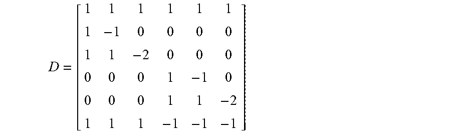
Wire coupling effects such as crosstalk on those subchannels may similarly be categorized as occurring between wires of the same densely-routed wire group, or imposed on the group from external sources such as another wire group. Transposing the second and third, and the fifth and sixth wire signals in matrix D produces matrix E, in which these effects are minimized.
##EQU00003##
Crosstalk between wires of the same group is reduced significantly by the described wire grouping and this modified code, because of the relative symmetry of the signaling within each wire group, which tends to balance positive and negative inter-wire capacitive coupling effects. As taught by [Shokrollahi II], this inter-group symmetry also helps to control the total energy emitted by the group that could inductively couple externally, by locally balancing wire current flows within the densely-routed wire group. In particular, in a first group of subchannels consisting of rows 2 and 3 of E, the signaling elements are locally symmetric, or balanced as between the first three wires, such that in the second row the +1 and -1 signal elements are on opposite sides of a center conductor carrying a zero, or middle value. The third row has a local symmetry by having positive values on the outer wires of the grouping of three conductors with a negative value in the middle (or with the reverse polarity of a positive in the middle with negative values on the outer wires). Similarly, this intra-wire group symmetry is repeated for the second group of subchannels (rows 4 and 5 of E) on the second grouping of three conductors forming another densely-routed wire group. In embodiments with more than two groups of densely-routed wire groups, a common mode vector of each group may be seen to form additional subchannels across the groups that display a global inter-group symmetry that is similar to the local intra-group symmetry. That is, in the same way that a subchannel having elements 1, 0, -1 (or elements 1, -2, 1) has a local symmetry within a three-wire group of densely-routed wires, the same type of inter-group symmetry across subgroups is present in a subchannel carried by 9 wires that make up three 3-wire densely-routed groups having elements 1, 1, 1, 0, 0, 0, -1, -1, -1, or a subchannel 1, 1, 1, -2, -2, -2, 1, 1, 1.
To control any residual external crosstalk effects, one embodiment introduces additional isolation spacing between adjacent wire groups, beyond the usual inter-wire spacing. Thus, as shown in FIG. 1, wire groups 110 and 120 are separated by spacing s rather than the spacing w used between wires of the same group. Relative spacings in one particular embodiment are 5 units per wire width W, 5 units for inter-wire spacing d, and 15 units for inter-group spacing s. Thus, a two group six wire microstripline signal path 112, 114, 116, 122, 124, 126 with such spacing will occupy 65 units of total width. By comparison, a legacy six wire three differential pair microstripline signal path laid out with comparable design rules occupies at least 75 units of total width, and can occupy as much as 95 units of width with more typical inter-pair spacing.
Inter-Group Skew Control
The Glasswing subchannel represented by row 6 of matrix D compares the summation of signals on wires 1, 2, 3 with the summation of signals on wires 4, 5, 6, i.e. between the two wire groups. Thus, this subchannel result will be influenced by any skew introduced by wire path differences between the two wire groups. For one representative practical embodiment operating at a 25 Gbps signaling rate (40 picoseconds per signaling unit interval) skew within each three wire group was limited to several picoseconds, while skew between groups could be as much as 10-15 picoseconds.
Conventional skew mitigation teachings suggest that variable delay elements be introduced into each wire signal path, allowing the "fast" wire signals to be delayed until concurrent with the "slow" wire signals. Such variable delay elements are typically implemented as chains of logic gates such as inverters, or as discrete element analog delay lines. Because there is no a priori way of identifying which wire group will be fast or slow, this suggests that a full set of six variable delay elements are used, with significant impact on cost, circuit complexity, and power consumption.
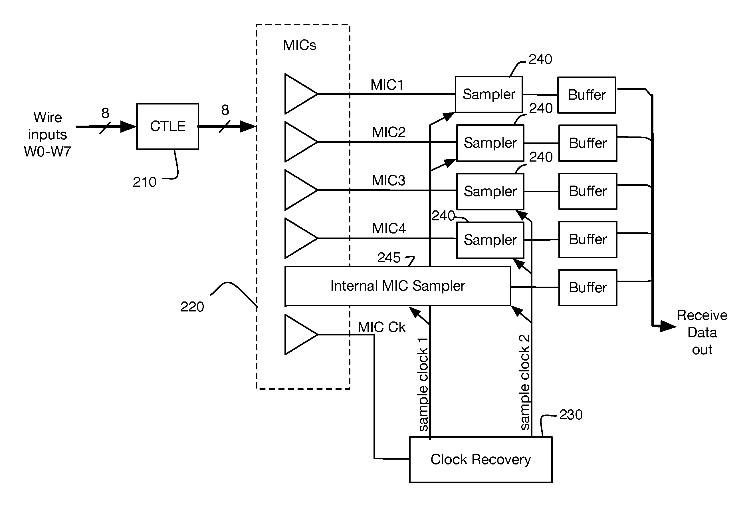
One alternative embodiment delays not the actual wire signals, but instead the sample timing associated with those wire signals. As seen in FIG. 2, a separate clock data alignment system is used to produce a sample timing clock for each densely-routed wire group. In the embodiment of FIG. 2, a clock signal is provided over a differential pair of wires (which, together with a 5b6w system configured as two 3-wire densely-routed groups, brings the total number of wires to 8). In alternative embodiments, a clock signal may be recovered from a MIC output corresponding to a clock-embedded sub-channel through known clock recovery techniques. Further, in some alternative embodiments, a clock signal may be embedded in a subchannel of the orthogonal code, and which may be a subchannel whose elements are carried in a single densely-routed wire group. In these various embodiments, the result of the first set of multi-input comparators configured as the second and third rows of matrix D may be sampled at time t, while the result of the second set of multi-input comparators configured as the fourth and fifth rows of matrix D may be sampled at, as an example, time t+15 picoseconds, if wires 4, 5, and 6 have 15 picoseconds of additional delay beyond that of wires 1, 2, and 3. Internal MIC sampler 245 may be referred to herein as a global MIC, as it is connected to all of the densely-routed wire groups. Alternatively, a global MIC may be a MIC connected to at least two densely-routed wire groups. In the embodiment shown in FIG. 2, it is connected to the first and second densely-routed wire groups.
Sampling of the final detected subchannel, described by the sixth row of matrix D may be more problematic due to skew between the two densely-routed wire groups, wherein the skew is dominated by a difference in the physical lengths of the two wire groups. Further, common mode signals present on the individual densely-routed wire groups may induce differing propagation delays that may further skew the densely-routed wire groups. In particular, a conventional multi-input comparator has only a single sample-able output, which depending on the embodiment either represents a digital comparison result derived from the weighted input terms, or the corresponding analog weighted summation of all input terms. In some embodiments, an apparatus includes a first set of multi-input comparators (MICs) connected to a first densely-routed wire group of a multi-wire bus, the first set of MICs configured to receive signal elements corresponding to a first group of symbols of a vector signaling codeword. In FIG. 2, the first set of MICs may include MIC1 and MIC2, MIC1, and the first densely-routed wire group may include wires W0, W1, and W2. The apparatus may further include a second set of MICs, such as MIC 3 and MIC4, connected to a second densely-routed wire group including wires W3, W4, and W5 of the multi-wire bus, the second set of MICs configured to receive signal elements corresponding to a second group of symbols of the vector signaling codeword. The apparatus may further include a global MIC, shown in FIG. 2 as internal MIC sampler 245, the global MIC connected to the first and second densely-routed wire groups and configured to receive signal elements corresponding to the first and second groups of symbols of the vector signaling codeword.
In some embodiments, the global MIC has a first input connected to all the wires of the first densely-routed wire group and a second input connected to all the wires of the second densely-routed wire group.
In some embodiments, the apparatus further includes a clock recovery circuit 230 for generating a first sampling clock for the first set of MICs and a second sampling clock for the second set of MICs, and wherein the global MIC obtains signal samples based on signal elements received from the first densely-routed wire group according to the first sampling clock, and obtains signal samples of signal elements based on signal elements received from the second densely-routed wire group according to the second sampling clock. In some embodiments, clock recovery circuit 230 obtains a symbol clock received on a differential pair of wires, such as wires W6 and W7 received at MIC ck, which may be a simple two-input differential comparator. Alternatively, the clock recovery circuit may receive a symbol clock from a MIC in the first or second set of MICs or the global MIC.
In some embodiments, the global MIC forms a comparison of a linear combination of the signal samples obtained from the first densely-routed wire group and the signal samples obtained from the second densely-routed wire group, and wherein the global MIC comprises a sampler for receiving a third sampling clock, the third sampling clock having a phase delay with respect to the first and second sampling clocks, the sampler configured to sample the comparison of the linear combination. In some embodiments, the comparison of the linear combination corresponds to a sum of the signal samples received from the first densely-routed wire group compared to a sum of the signal samples received from the second densely-routed wire group.
In some embodiments, the first and second densely-routed wire groups comprise intra-group symmetry with respect to corresponding sub-channel vectors carried by the respective densely-route wire groups. In some embodiments, the first and second densely-routed wire groups are separated by an isolation medium.
In some embodiments, the apparatus may be extended to include a third set of MICs connect to a third densely-routed wire group of the multi-wire bus, the third set of MICs configured to receive signal elements corresponding to a third group of symbols of the vector signaling codeword, and wherein the global MIC is further connected to the third densely-routed wire group and configured to receive signal elements corresponding to the third group of symbols of the vector signaling codeword.
FIG. 3 is a block diagram showing one alternative embodiment for decoding such a subchannel spanning two input wire groups that may have different timing characteristics. For purposes of illustration and without implying limitation, all elements typically seen in the signal path are shown, although some may be omitted in some embodiments, some may be shared with other receiver subsystems, and some elements may be combined, as in a combination MIC and sampler.
One embodiment of the global MIC shown in FIG. 3 includes two summation nodes 320 and 321, the first producing an analog summation of wires 1, 2, 3, and the second producing an analog summation of wires 4, 5, 6. The analog value of these two results are captured at times t.sub.1 and t.sub.2 using, as examples offered without limitation, analog sample-and-hold or integrate-and-hold circuits 330 and 331, respectively. The resulting values are then compared at a time t.sub.3 equal or later than the later of times t.sub.1 and t.sub.2 with the comparison result provided as the detected subchannel result.
At the system level, FIG. 2 illustrates times t.sub.1 and t.sub.2 as being identified by clock signals labeled "sample clock 1" and "sample clock 2" produced by receive clock recovery subsystem 230, those clocks also being associated with optimal sampling times for first wire group subchannels MIC1/MIC2, and second wire group subchannels MIC3/MIC4 respectively.
In FIG. 3, wire signals w1, w2, w3, w4, w5, and w6 are processed by Continuous Time Linear Equalizers (CTLEs) 310, 311, 312, 313, 314, 315 respectively. In some embodiments, the frequency-dependent filtering or amplification provided by CTLE is not used. Summation node 320 produces an analog summation of signals received from wires w1, w2, and w3 (i.e. a first wire group,) which is then sampled 330 using clock CK1 at time t.sub.1 associated with the optimum sampling interval for the first wire group. Similarly, summation node 321 produces an analog summation of signals received from wires w4, w5, w6 (i.e. a second wire group,) which is then sampled 331 using clock CK2 at time t.sub.2 associated with the optimum sampling interval for the second wire group. The resulting sampled values are presented to multi-input comparator 340, completing detection of the desired subchannel as described in matrix E. In some embodiments, the detected subchannel result is sampled 350 (as one example, using a combined MIC/sampler circuit) using clock CK3 at time t.sub.3, which is equal or later than the later of times t.sub.1 and t.sub.2.
A first alternative embodiment holds only the earlier of the two analog summation signals, performing a clocked comparison between it and the other analog summation signal at the later of the two times.
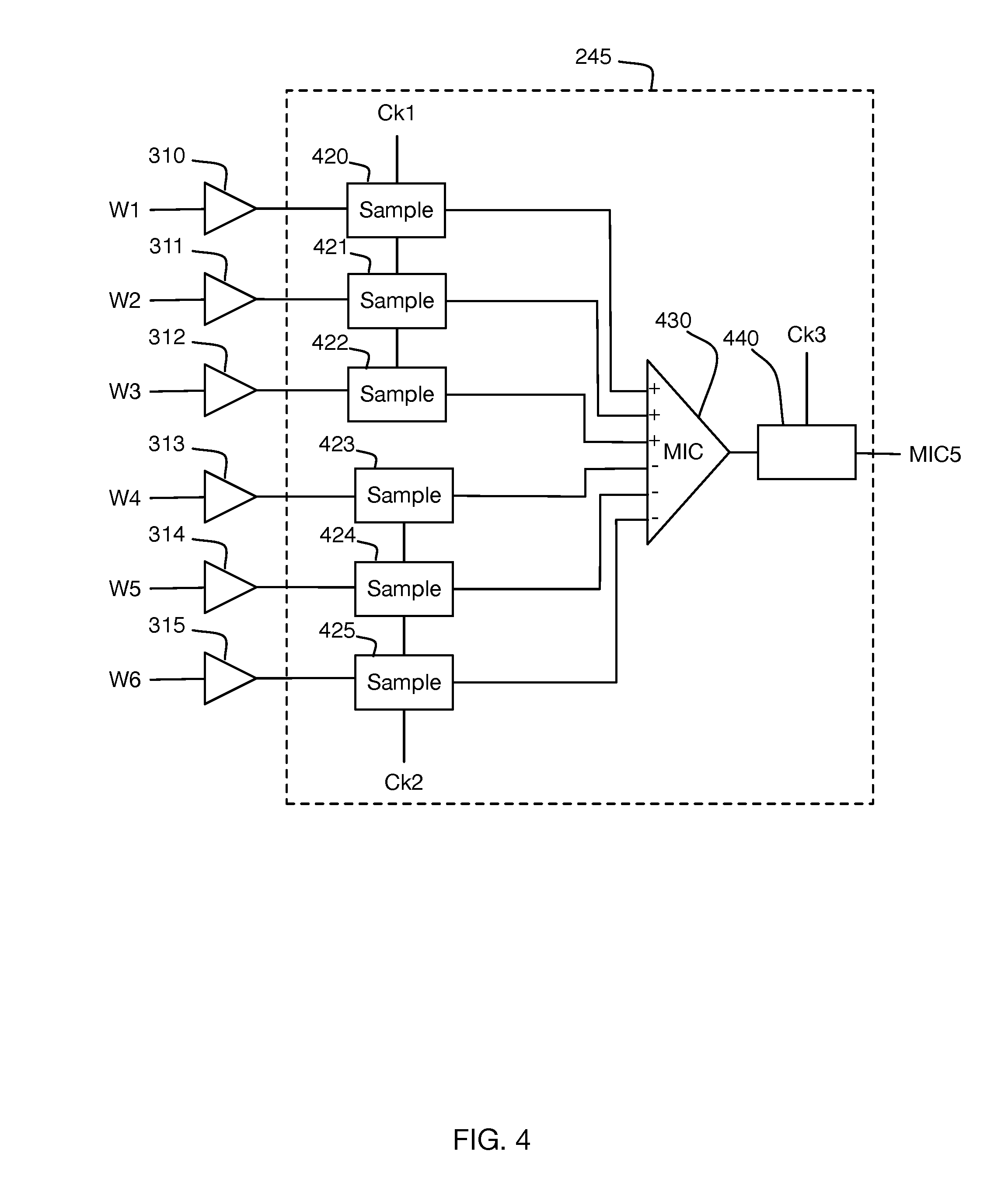
A second embodiment shown in FIG. 4 retains the conventional six input global MIC used to detect the subchannel corresponding to the sixth row of matrix E, by pre-sampling the wire signal inputs, their analog values being captured at one of times t.sub.1 and t.sub.2 using, as examples offered without limitation, analog sample-and-hold or integrate-and-hold circuits. The resulting values are then presented to the MIC, with the result available at a time equal or later than the later of times t.sub.1 and t.sub.2.
In FIG. 4, wire signals w1, w2, w3, w4, w5, and w6 are processed by Continuous Time Linear Equalizers (CTLEs) 310, 311, 312, 313, 314, 315 respectively. In some embodiments, the frequency-dependent filtering or amplification provided by CTLE is not used. The processed signals are then individually sampled 420, 421, 422, 423, 424, 425, with signals associated with a first wire group being sampled at time t.sub.1 using clock CK1, and signals associated with a second wire group being sampled at time t.sub.2 using clock CK2. The resulting sampled values are presented to multi-input comparator 430, completing detection of the desired subchannel as described in matrix E. In some embodiments, the detected subchannel result is sampled 440 (as one example, using a combined MIC/sampler circuit) using clock CK3 at time t.sub.3, which is equal or later than the later of times t.sub.1 and t.sub.2.
A first alternative embodiment samples or holds only the earlier of the two wire group signals, performing a sampled MIC detection using those signals and the other wire group signals at the later of the two times.
Additional mitigation of the increased skew seen between wire groups may also be obtained by extending the effective detection unit intervals on the relevant subchannels. One embodiment providing such mitigation transmits data on the subchannel corresponding to the sixth row of matrix E at one-half rate, as one example by repeating each data value presented to the encoder for that subchannel. The resulting extended time between transitions at the received MIC output may either be sampled at one half rate, or may be sampled at normal unit intervals with every other sample result being ignored as redundant or occurring during signal transitions.
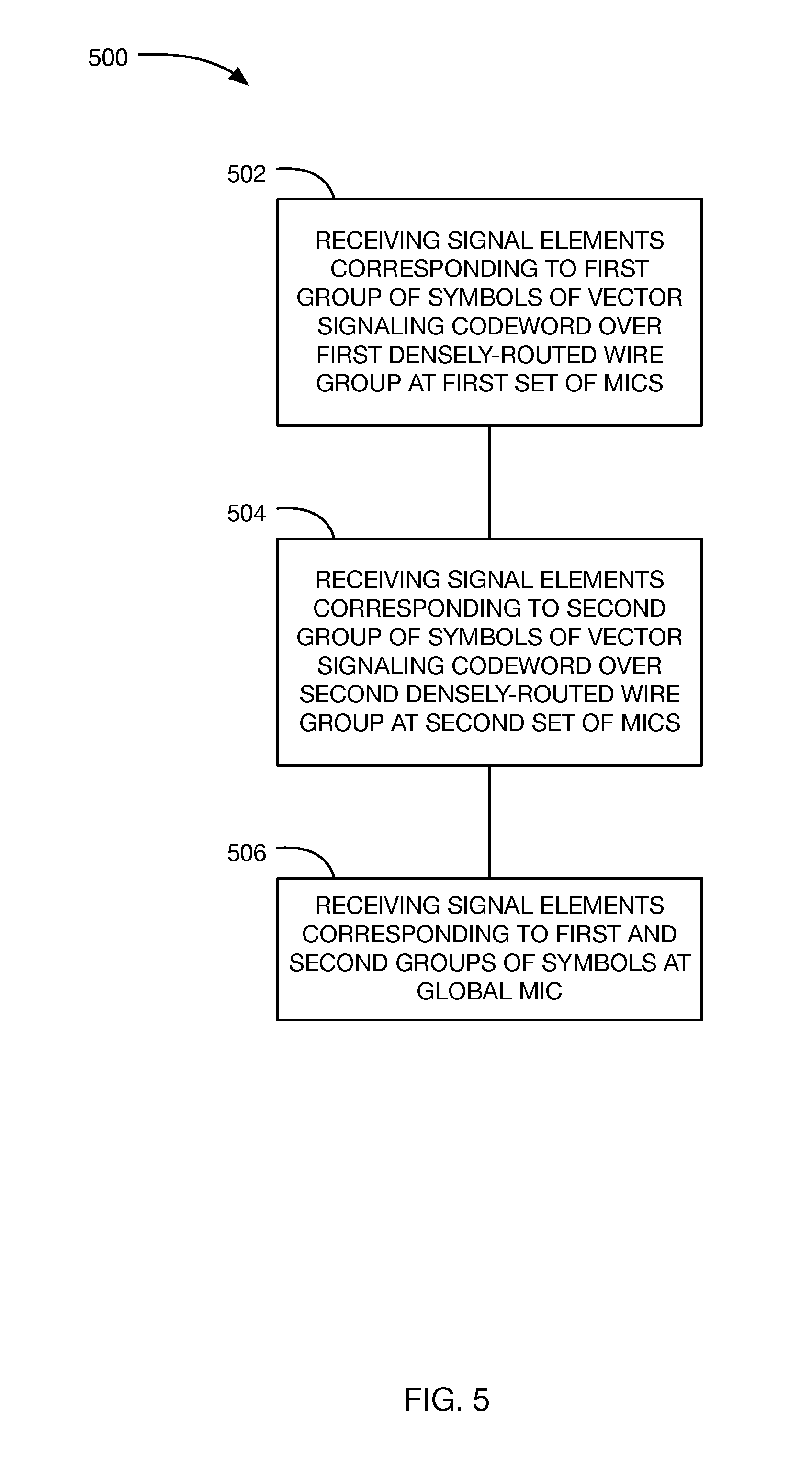
FIG. 5 is a flowchart of a method 500, in accordance with some embodiments. As shown, method 500 includes receiving 502 signal elements corresponding to a first group of symbols of a vector signaling codeword over a first densely-routed wire group of a multi-wire bus at a first set of MICs, receiving 504 signal elements corresponding to a second group of symbols of the vector signaling codeword over a second densely-routed wire group of the multi-wire bus at a second set of MICs, and receiving signal elements corresponding to the first and the second groups of symbols of the vector signaling codeword at a global MIC.
In some embodiments, the symbols of the vector signaling code represent a superposition of a plurality of subchannel vectors, each sub-channel vector weighted by a corresponding antipodal weight. In some embodiments, the first group of symbols of the vector signaling codeword correspond to a superposition of a first subset of the plurality of subchannel vectors and wherein the second group of symbols of the vector signaling codeword correspond to a superposition of a second subset of the plurality of subchannel vectors. For example, in the first group of symbols may correspond to symbols received on wires 1, 2, and 3, and the second group of symbols may correspond to symbols received on wires 4, 5, and 6 in accordance with the embodiment described with respect to FIG. 2. The symbols received on wires 1, 2, and 3 are formed using a summation of signal components provided by subchannel vectors corresponding to rows 2, 3, and 6 of matrix D. Similarly, symbols received on wires 4, 5, and 6 are formed using a summation of signal components provided by subchannel vectors corresponding to rows 4, 5, and 6 of matrix D. In such an embodiment, the first and second subsets of the plurality of subchannel vectors share a single subchannel vector corresponding to row 6.
In some embodiments, the signal elements of the first group of subchannel vectors are locally symmetric over the first densely-routed wire group and the signal elements of the second group of subchannel vectors are locally symmetric over the second densely-routed wire group. Such symmetry is illustrated above regarding the permutations of the columns of matrix D to obtain matrix E. As described above, the first densely-routed group of wires 1, 2, and 3 carry a superposition of signal components of subchannel vectors corresponding to rows 2, 3 and 6 of the matrix. By providing subchannel symmetry, the crosstalk associated with each subchannel vector is reduced. The subchannel vector corresponding to row 2 has differential signal components on wires 1 and 3, which reduces crosstalk compared to the signal components being on wires 1 and 2. Similarly, the subchannel vector corresponding to row 3 has signal component values of `1` on wires 1 and 3, with a signal component value of `-2` in the middle on wire 2, further reducing crosstalk. As the signal component values put on wires 1, 2, and 3 from the subchannel vector corresponding to row 6 of the matrix are all equal, there is no change in crosstalk due to the permutation of the columns of the matrix.
In some embodiments, the method further includes generating a first set of sampled outputs of the first set of MICs using a first sampling clock and generating a second set of sampled outputs of the second set of MICs using a second sampling clock, and forming a comparison of (i) a sum of the first set of sampled outputs and (ii) the second set of sampled outputs, and sampling the comparison using a third sampling clock. In some embodiments, the third sampling clock has a delay with respect to the first and second sampling clocks, and may be formed using the first and second sampling clocks, or using another means of generating a sampling clock.
In some embodiments, the first and second densely-routed wire group comprises three conductors. In alternative embodiments, the first densely-routed wire group comprises three conductors and the second densely-routed wire group comprises two conductors. Other densely-routed wire group formats may also be plausible, such as three densely-routed wire groups each having three wires. In such and embodiment having three densely-routed wire groups, the method further includes receiving signal elements corresponding to a third group of symbols of the vector signaling codeword over a third densely-routed wire group of the multi-wire bus at a third set of MICs, and wherein the global MIC is further configured to receive the signal elements corresponding to the third group of symbols of the vector signaling codeword.
Extension to Additional Wire Groups
In some embodiments, the wire arrangements of FIG. 1 may be extended to support additional wiring groups beyond the two groups of the previous example by introducing another inter-group space s and another set of wires of width w and spacing d.
As one familiar with vector signaling codes will observe, the same coding methodologies used for encoding signals on individual wires may be applied to encoding the common mode values of wire groups. Without limitation, these methods include differential signaling between the common mode values of pairs of groups (as in the previous example), differential signaling between the sum of common modes on two groups versus the common mode of another group, differential signaling between the sum of common modes of two groups versus the sum of common modes of two other groups, and extensions of these methods to larger sets of groups.
Normalizing Subchannel Gain
It may be observed that the MICs defined by matrix rows 1, 3, and 5 of matrices D and E produce output values of .+-.2/3, whereas the MICs defined by matrix rows 2 and 4 produce output values of .+-.1. The loss in vertical eye opening compared to differential signaling is therefore 20*log 10(3)=.about.9.5 dB. This output level variation is the result of our loosened definition of orthogonality for the receive matrix, as the non-unity values of the diagonal M.sup.TM=D represent non-unity gains for the corresponding sub-channels. In some embodiments, normalizing the matrix (i.e. scaling its elements such that the diagonal values are 1), results in a system having constant unity gain across all sub-channels. However, such known normalization methods may lead to suboptimal embodiments as the large number of distinct normalized coefficient values, in many cases including irrational values, are difficult to embody in a practical system.
At least one embodiment retains the un-normalized matrix with its convenient-to-implement coefficient values, and instead compensates for the variation of sub-channel amplitude by modifying the input signal amplitudes modulating the various sub-channel. For example, a hypothetical system having eight sub-channels of unity gain and one sub-channel of 0.8 gain will ultimately be SNR limited by the latter output. Thus, increasing the last sub-channel's transmission input to {+1.2, -1.2} rather than {+1, -1} will bring up the corresponding channel output. Alternatively, decreasing all other sub-channel inputs to {+0.8, -0.8} will lower the corresponding channel outputs, such that all channels have equal output levels and use less transmit power.
This compensation technique is not without cost, however. As taught by [Shokrollahi III], modifying the input vector in this manner leads to an increase in the alphabet size needed (and thus, the number of discrete signal levels the transmitter must generate) to communicate the codewords over the channel. [Shokrollahi III] teaches numeric methods to select suitable modulation amplitudes that result in closer matching of sub-channel outputs with minimal expansion of the alphabet size.
Applying the procedure taught by [Shokrollahi III], the optimal initial code set for Glasswing is calculated to be (0, .+-.3/8, .+-.1/4, .+-.3/8, .+-.1/4, .+-.3/8) with the corresponding code having an alphabet of size 10 given by (1, 7/8, 1/2, 1/4, 1/8, -1/8, -1/4, -1/2, -7/8, -1). The resulting codewords are shown in Table 1, with the new code herein called the 5b6w_10_5 code.
TABLE-US-00001 TABLE 1 .+-. [1, 1/4, -1/8, 1/4, -1/2, -7/8] .+-. [1, 1/4, -1/8, -1/4, -1, 1/8] .+-. [1/4, 1, -1/8, 1/4, -1/2, -7/8] .+-. [1/4, 1, -1/8, -1/4, -1, 1/8] .+-. [1/2, -1/4, 7/8, 1/4, -1/2, -7/8] .+-. [1/2, -1/4, 7/8, -1/4, -1, 1/8] .+-. [-1/4, 1/2, 7/8, 1/4, -1/2, -7/8] .+-. [-1/4, 1/2, 7/8, -1/4, -1, 1/8] .+-. [1, 1/4, -1/8, -1/2, 1/4, -7/8] .+-. [1, 1/4, -1/8, -1, -1/4, 1/8] .+-. [1/4, 1, -1/8, -1/2, 1/4, -7/8] .+-. [1/4, 1, -1/8, -1, -1/4, 1/8] .+-. [1/2, -1/4, 7/8, -1/2, 1/4, -7/8] .+-. [1/2, -1/4, 7/8, -1, -1/4, 1/8] .+-. [-1/4, 1/2, 7/8, -1/2, 1/4, -7/8] .+-. [-1/4, 1/2, 7/8, -1, -1/4, 1/8]
With this code, all MICs as defined by matrix E produce output values of .+-.3/4. The increase in vertical eye opening compared to the unmodified 5b6w code is 20*log 10((3/4)/(2/3))=.about.1 dB. The termination power of 5b6w_10_5 is about 88% of the termination power of the unmodified 5b6w code, so even at a smaller termination power, 5b6w_10_5 leads to a fractionally improved vertical eye opening. However, the implementation cost to obtain this improvement is the added complexity within the transmitter to encode data into an internal representation capable of selecting among ten rather than four symbol values per wire, and line drivers capable of generating ten discrete output levels rather than four. Such a transmitter embodiment would be fully compatible with any Glasswing receiver defined by matrix E, and would use less line driver power than an unmodified 5b6w transmit driver. Because of this generally disadvantageous cost/benefit tradeoff, most embodiments of Glasswing transmitters are expected to utilize unmodified 5b6w signal levels; where they are cost-effective, alternative embodiments incorporating the 5b6w_10_5 modifications may transparently be interchanged and/or interoperate with unmodified ones.
Addressing Transistor Mismatch
Especially with very small integrated circuit feature sizes, there can be considerable mismatch between "identical" transistors in a circuit design. As examples, consider two MIC designs as taught by [Holden I] for detection of the second and third rows of matrix E. The MIC detecting the second row utilizes a differential comparator input having one transistor on each input leg, making it more susceptible to process variations between those transistors, while the MIC detecting the third row has two transistors on each input leg, reducing its susceptibility to process variations.
One embodiment addresses such susceptibilities by increasing the number of transistors per differential input leg by, as one example, paralleling two or more transistors per input signal rather than utilizing a single transistor. This paralleling may be seen in matrix F,
##EQU00004## which differs from matrix E in that its second and fourth rows have been multiplied by three, and its third and fifth rows have been multiplied by two. Thus, a MIC embodying the second row of matrix F would utilize three paralleled transistors per differential input leg where a MIC embodying the second row of matrix E would use a single transistor per differential input leg.
EMBODIMENTS
Following are some embodiments that incorporate various aspects of the signaling and associated wire groupings described above. The term "normal matrix" is used to refer to matrices with integer values for ease of understanding, with the normalization factor specified separately. The term "symmetric-eye matrix" specifies the matrix variation that provides equal eye openings at the output of the receive comparators/amplifiers.
2b3w:
Normal Matrix:
##EQU00005## Normalization factor=2. The alphabet is {1,0,-1}. Eye openings are .+-.1, .+-. 3/2. Symmetric-Eye Matrix:
##EQU00006## Normalization factor=5. The alphabet is {1, 4/5, 1/5, -1/5, -4/5, -1}. All eye openings are .+-. 6/5. Routing can be done by having tight skew match across wires 1 and 3, and less skew match on the middle wire.
4b5w:
Normal Matrix:
##EQU00007## Normalization factor=4. The alphabet in this case is {1, 1/3, 0, -1/3, -1}. Eye openings are .+-.1/2, .+-.3/4, .+-.1/2, .+-. 5/4. Symmetric-Eye Matrix:
##EQU00008## Normalization factor=37 to provide values between .+-.1. The alphabet size is 16, and the alphabet is [-37, -33, -32, -17, -13, -8, -7, -3, 3, 7, 8, 13, 17, 32, 33, 37]/37. All eye openings are 30/37.about.0.81.
Routing is in a dense group of 3 wires and a dense group of 2 wires: spacing of w-space-w-space-w 3.times.space w-space-w where space is 5 units, and w is 5 units. Skew between the group of 3 and group of 2 can be handled similarly to what is described for GW and skew between two groups of 3 wires.
8b9w:
Normal Matrix:
##EQU00009## Normalization factor=4. The alphabet in this case is {1, 1/2, 0, -1/2, -1]. Eye openings are .+-.1/2, .+-.3/4, .+-.1/2, .+-.3/4, .+-.1/2. .+-.1/2, .+-.3/4. Symmetric-Eye Matrix:
##EQU00010## Normalization factor=10. The alphabet in this case is of size 21 and equals [-10, -9, -8, -6, -5, -4, -3, -2, -1, 0, 1, 2, 3, 4, 5, 6, 8, 9, 10]/10. The eye openings are .+-.3/5.
Routing can be done in groups of three wires, distance 5 between wires in each group, distance 15 between groups. The two outer three wire groups have closer matching between groups than matching with the middle group of three wires.
Example signal levels, signal frequencies, and physical dimensions described herein are provided for purposes of explanation, and are not limiting. Different vector signaling codes may be used, communicated using more or fewer wires per group, fewer or greater numbers of signal levels per wire, and/or with different code word constraints. For convenience, signal levels are described herein as voltages, rather than their equivalent current values.
Other embodiments may utilize different signaling levels, connection topology, termination methods, and/or other physical interfaces, including optical, inductive, capacitive, or electrical interconnection. Similarly, examples based on unidirectional communication from transmitter to receiver are presented for clarity of description; combined transmitter-receiver embodiments and bidirectional communication embodiments are also explicitly in accordance with some embodiments.
The examples presented herein illustrate the use of vector signaling codes carried by parallel transmission line interconnections for intra-chip and chip-to-chip communication. However, those exemplary details should not be seen as limiting the scope of the described embodiments. The methods disclosed in this application are equally applicable to other interconnection topologies and other communication media including optical, capacitive, inductive, and wireless communications which may rely on any of the characteristics of the described embodiments, including but not limited to communications protocol, signaling methods, and physical interface characteristics. Thus, descriptive terms such as "voltage" or "signal level" should be considered to include equivalents in other measurement systems, such as "current", "optical intensity", "RF modulation", etc. As used herein, the term "signal" includes any suitable behavior and/or attribute of a physical phenomenon capable of conveying information. The information conveyed by such signals may be tangible and non-transitory.
* * * * *
References
D00000
D00001
D00002
D00003
D00004
D00005
M00001
M00002
M00003
M00004
M00005
M00006
M00007
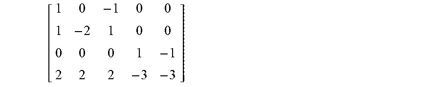
M00008
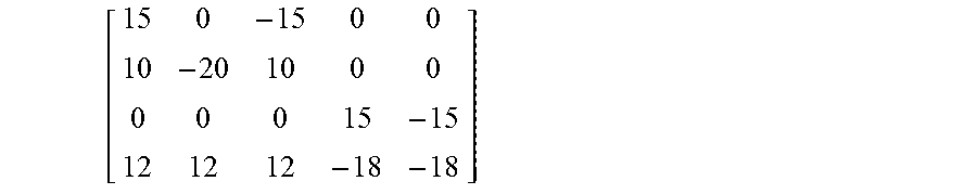
M00009

M00010

XML
uspto.report is an independent third-party trademark research tool that is not affiliated, endorsed, or sponsored by the United States Patent and Trademark Office (USPTO) or any other governmental organization. The information provided by uspto.report is based on publicly available data at the time of writing and is intended for informational purposes only.
While we strive to provide accurate and up-to-date information, we do not guarantee the accuracy, completeness, reliability, or suitability of the information displayed on this site. The use of this site is at your own risk. Any reliance you place on such information is therefore strictly at your own risk.
All official trademark data, including owner information, should be verified by visiting the official USPTO website at www.uspto.gov. This site is not intended to replace professional legal advice and should not be used as a substitute for consulting with a legal professional who is knowledgeable about trademark law.