Photovoltaic device
Archer , et al.
U.S. patent number 10,326,033 [Application Number 13/772,043] was granted by the patent office on 2019-06-18 for photovoltaic device. This patent grant is currently assigned to ALTA DEVICES, INC.. The grantee listed for this patent is Alta Devices, Inc.. Invention is credited to Melissa J. Archer, Thomas J. Gmitter, Gang He, Gregg Higashi.


View All Diagrams
| United States Patent | 10,326,033 |
| Archer , et al. | June 18, 2019 |
Photovoltaic device
Abstract
Methods and apparatus are provided for converting electromagnetic radiation, such as solar energy, into electric energy with increased efficiency when compared to conventional solar cells. One embodiment of the present invention provides a photovoltaic (PV) device. The PV device comprises an absorber layer made of a compound semiconductor; and an emitter layer located closer than the absorber layer to a first side of the device. The PV device includes a p-n junction formed between the emitter layer and the absorber layer, the p-n junction causing a voltage to be generated in the device in response to the device being exposed to light at a second side of the device. Such innovations may allow for greater efficiency and flexibility in PV devices when compared to conventional solar cells.
| Inventors: | Archer; Melissa J. (San Jose, CA), Gmitter; Thomas J. (Sunnyvale, CA), He; Gang (Cupertino, CA), Higashi; Gregg (San Jose, CA) | ||||||||||
|---|---|---|---|---|---|---|---|---|---|---|---|
| Applicant: |
|
||||||||||
| Assignee: | ALTA DEVICES, INC. (Sunnyvale,
CA) |
||||||||||
| Family ID: | 42120001 | ||||||||||
| Appl. No.: | 13/772,043 | ||||||||||
| Filed: | February 20, 2013 |
Prior Publication Data
| Document Identifier | Publication Date | |
|---|---|---|
| US 20130153013 A1 | Jun 20, 2013 | |
Related U.S. Patent Documents
| Application Number | Filing Date | Patent Number | Issue Date | ||
|---|---|---|---|---|---|
| 12605108 | Oct 23, 2009 | 8937244 | |||
| 61107954 | Oct 23, 2008 | ||||
| Current U.S. Class: | 1/1 |
| Current CPC Class: | H01L 31/0236 (20130101); H01L 31/0693 (20130101); H01L 31/022441 (20130101); H01L 31/056 (20141201); H01L 31/03046 (20130101); H01L 31/065 (20130101); H01L 31/02363 (20130101); H01L 31/0735 (20130101); H01L 31/0682 (20130101); H01L 31/0304 (20130101); Y02E 10/50 (20130101); Y02E 10/52 (20130101); Y02E 10/544 (20130101); Y02E 10/547 (20130101) |
| Current International Class: | H01L 31/00 (20060101); H01L 31/0224 (20060101); H01L 31/065 (20120101); H01L 31/0693 (20120101); H01L 31/0236 (20060101); H01L 31/068 (20120101); H01L 31/0304 (20060101); H01L 31/0735 (20120101) |
| Field of Search: | ;136/244,252,255,256,262 |
References Cited [Referenced By]
U.S. Patent Documents
| 3615853 | October 1971 | Paine et al. |
| 3988167 | October 1976 | Kressel |
| 3990101 | November 1976 | Ettenberg et al. |
| 4015280 | March 1977 | Matsushita et al. |
| 4017332 | April 1977 | James |
| 4094704 | June 1978 | Milnes |
| 4107723 | August 1978 | Kamath |
| 4191593 | March 1980 | Cacheux |
| 4197141 | April 1980 | Bozler et al. |
| 4295002 | October 1981 | Chappell et al. |
| 4338480 | July 1982 | Antypas et al. |
| 4385198 | May 1983 | Rahilly |
| 4400221 | August 1983 | Rahilly |
| 4410758 | October 1983 | Grolitzer |
| 4419533 | December 1983 | Czubatyj et al. |
| 4444992 | April 1984 | Cox, III |
| 4479027 | October 1984 | Todorof |
| 4497974 | February 1985 | Deckman et al. |
| 4543441 | September 1985 | Kumada et al. |
| 4571448 | February 1986 | Barnett |
| 4582952 | April 1986 | McNeely |
| 4633030 | December 1986 | Cook |
| 4667059 | May 1987 | Olson |
| 4775639 | October 1988 | Yoshida |
| 4889656 | December 1989 | Flynn et al. |
| 4916503 | April 1990 | Uematsu et al. |
| 4989059 | January 1991 | Micheels et al. |
| 4997491 | March 1991 | Hokuyo et al. |
| 5101260 | March 1992 | Nath et al. |
| 5103268 | April 1992 | Yin et al. |
| 5116427 | May 1992 | Fan et al. |
| 5136351 | August 1992 | Inoue et al. |
| 5217539 | June 1993 | Fraas et al. |
| 5223043 | June 1993 | Olson et al. |
| 5316593 | May 1994 | Olson et al. |
| 5330585 | July 1994 | Chang et al. |
| 5342453 | August 1994 | Olson |
| 5356488 | October 1994 | Hezel |
| 5376185 | December 1994 | Wanlass |
| 5385960 | January 1995 | Emmons et al. |
| 5465009 | November 1995 | Drabik et al. |
| 5468652 | November 1995 | Gee |
| 6107563 | August 2000 | Nakanishi et al. |
| 6166218 | December 2000 | Ravichandran |
| 6166318 | December 2000 | Freeouf |
| 6229084 | May 2001 | Katsu |
| 6231931 | May 2001 | Blazey et al. |
| 6255580 | July 2001 | Karam et al. |
| 6372981 | April 2002 | Ueda et al. |
| 6534336 | March 2003 | Iwane et al. |
| 6617508 | September 2003 | Kilmer et al. |
| 7038250 | May 2006 | Sugiyama et al. |
| 7875945 | January 2011 | Krasnov et al. |
| 8183081 | May 2012 | Weidman et al. |
| 8258596 | September 2012 | Nasuno et al. |
| 8664515 | March 2014 | Hong et al. |
| 8697553 | April 2014 | Adibi et al. |
| 9099595 | August 2015 | King et al. |
| 2001/0027805 | October 2001 | Ho et al. |
| 2002/0000244 | January 2002 | Zaidi |
| 2002/0053683 | May 2002 | Hill et al. |
| 2002/0144724 | October 2002 | Kilmer et al. |
| 2002/0179141 | December 2002 | Ho et al. |
| 2003/0070707 | April 2003 | King et al. |
| 2003/0140962 | July 2003 | Sharps et al. |
| 2003/0222278 | December 2003 | Liu et al. |
| 2004/0112426 | June 2004 | Hagino |
| 2004/0166681 | August 2004 | Iles et al. |
| 2004/0200523 | October 2004 | King et al. |
| 2005/0022863 | February 2005 | Agostinelli et al. |
| 2006/0081963 | April 2006 | Rehder et al. |
| 2006/0090790 | May 2006 | Kobayashi et al. |
| 2006/0144435 | July 2006 | Wanlass |
| 2006/0162767 | July 2006 | Mascarenhas et al. |
| 2006/0207651 | September 2006 | Posthuma et al. |
| 2006/0255340 | November 2006 | Manivannan et al. |
| 2007/0131275 | June 2007 | Kinsey et al. |
| 2007/0137695 | June 2007 | Fetzer et al. |
| 2007/0137698 | June 2007 | Wanlass et al. |
| 2007/0151596 | July 2007 | Nasuno et al. |
| 2007/0166862 | July 2007 | Kim et al. |
| 2007/0199591 | August 2007 | Harder et al. |
| 2007/0235074 | October 2007 | Henley et al. |
| 2007/0277874 | December 2007 | Dawson-Elli et al. |
| 2008/0128020 | June 2008 | Zafar et al. |
| 2008/0245409 | October 2008 | Varghese et al. |
| 2009/0151784 | June 2009 | Luan et al. |
| 2009/0283802 | November 2009 | Henderson et al. |
| 2010/0006143 | January 2010 | Weiser |
| 2010/0015751 | January 2010 | Weidman et al. |
| 2010/0055397 | March 2010 | Kurihara et al. |
| 2010/0065117 | March 2010 | Kim et al. |
| 2010/0089443 | April 2010 | Bloomstein et al. |
| 2010/0096010 | April 2010 | Welser |
| 2010/0126552 | May 2010 | Kizilyalli et al. |
| 2010/0126570 | May 2010 | Kizilyalli et al. |
| 2010/0126571 | May 2010 | Kizilyalli et al. |
| 2010/0126572 | May 2010 | Kizilyalli et al. |
| 2010/0132774 | June 2010 | Borden |
| 2010/0132780 | June 2010 | Kizilyalli et al. |
| 2010/0193002 | August 2010 | Dimroth et al. |
| 2010/0294356 | November 2010 | Parikh et al. |
| 2011/0088771 | April 2011 | Lin et al. |
| 2011/0108098 | May 2011 | Kapur |
| 2011/0156000 | June 2011 | Cheng |
| 2011/0214728 | September 2011 | Veerasamy |
| 2011/0244692 | October 2011 | Jeong et al. |
| 2011/0290322 | December 2011 | Meguro et al. |
| 2012/0024336 | February 2012 | Hwang |
| 2012/0031478 | February 2012 | Boisvert et al. |
| 2012/0055541 | March 2012 | Granek et al. |
| 2012/0067423 | March 2012 | Lochtefeld et al. |
| 2012/0104411 | May 2012 | Iza et al. |
| 2012/0125256 | May 2012 | Kramer et al. |
| 2012/0132930 | May 2012 | Young et al. |
| 2012/0160296 | June 2012 | Laparra et al. |
| 2012/0164796 | June 2012 | Lowenthal et al. |
| 2012/0227805 | September 2012 | Hermle et al. |
| 2013/0026481 | January 2013 | Xu et al. |
| 2013/0112258 | May 2013 | Park et al. |
| 2013/0220396 | August 2013 | Janssen et al. |
| 2013/0288418 | October 2013 | Wang et al. |
| 2014/0076386 | March 2014 | King et al. |
| 2014/0261611 | September 2014 | King et al. |
| 2014/0312373 | October 2014 | Donofrio |
| 2015/0171261 | June 2015 | Domine |
| 0595634 | May 1994 | EP | |||
| 63-211775 | Sep 1988 | JP | |||
| 3-285368 | Dec 1991 | JP | |||
| 06-244443 | Sep 1994 | JP | |||
| 07-007148 | Jan 1995 | JP | |||
| 8-130321 | May 1996 | JP | |||
| 10-0762772 | Oct 2007 | KR | |||
| WO 02065553 | Aug 2002 | WO | |||
| 2008100603 | Aug 2008 | WO | |||
Other References
|
M M. Sanfacon et al, "Analysis of AlGaAs/GaAs Solar Cell Structures by Optical Reflectance Spectroscopy" IEEE Transactions on Electron Devices, vol. 37, No. 2, Feb. 1990, pp. 450-454. cited by applicant . Q. M. Zhang et al., "Effects of Displaced p-n Junction of Heterojunction Bipolar Transistors", IEEE Transactions on Electron Devices, vol. 39, No. 11, Nov. 1992, pp. 2430-2437. cited by applicant . Peter A. Lewis, "Pigment Handbook vol. I: Properties and Economics, 2nd Edition", John Wiley & Sons, New York, pp. 790-791 (1988). cited by applicant . B. H. Floyd, et al., "An N--AlGaAs P--GaAs Graded Heterojunction for High Concentration Ratios," pp. 81-86, IEEE, 1987. cited by applicant . Hiroshi Yamaguchi, et al., "Development Status of "Space Solar Sheet"", IEEE PVSC Proceedings, 2008. cited by applicant . Tatsuya Takamoto, et al., "Paper-Thin InGaP/GaAs Solar Cells", IEEE PVSC Proceedings, pp. 1769-1772, 2006. cited by applicant . Nielson et al. "Microfabrication of microsystem-enabled photovoltaic (MEPV) cells." Proceedings of the International Society of Optics and Photonics (SPIE) [online], (Jan. 25, 2011) Retreived from the internet: <URL: http://photovoltaics.sandia.gov/Pubs_2010/2011/Microfab_of_MEPV_- Cells_SPIE_2011.pdf> See entire document especially Figure 5, p. 5. cited by applicant . Van Wijngaarden et al. "Direct Imaging of Propagation and Damping of Near-Resonance Surface Plasmon Polaritons using Cathodoluminescence Spectroscopy" (Jun. 1, 2006) Appl. Phys. Left. 88, 221111, pp. 1-3. cited by applicant . Pacifici et al. "Quantitative Determination of Optical Transmission through Subwavelength Slit Arrays in Ag films: The Essential role of Surface Wave Interference and Local Coupling between Adjacent Slits" (Oct. 22, 2007) Thomas J. Watson Lab. of Appl. Phys., pp. 1-4. cited by applicant . Park et al. "Surface Plasmon Enhanced Photoluminescence of Conjugated Polymers" (Apr. 17, 2007) Appl. Phys. Letters 90, 161107, pp. 1-3. cited by applicant . Tanabe et al. "Direct-bonded GaAs/InGaAs Tandem Solar Cell" (Sep. 6, 2006) Appl. Phys. Left. 89, 102106, pp. 1-3. cited by applicant . Dionne et al. "Highly Confined Photon Transport in Subwavelength Metallic Slot Waveguides" (Jun. 20, 2006) Nano Lett., vol. 6, No. 9, pp. 1928-1932. cited by applicant . Biteen et al. "Spectral Tuning of Plasmon-enhanced Silicon Quantum Dot Luminescence" (Mar. 31, 2006) Applied Physics Letters 88, 131109, pp. 1-3. cited by applicant . Aisaka et al. "Enhancement of upconversion Luminescence of Er Doped Al2O3 Films by Ag Islands Films" (Apr. 1, 2008) Applied Physics Letters 92, 132105, pp. 1-3. cited by applicant . Lezec et al. "Negative Refraction at Visible Frequencies" (Apr. 20, 2007) Science, vol. 316, pp. 430-432. cited by applicant . Pillai et al. "Enhanced emission from Si-based Light-emitting Diodes using Surface Plasmons" (Apr. 17, 2006) Applied Physics Letters, 88, 161102, pp. 1-3. cited by applicant . "Volmer-Weber and Stranski-Krastanov InAs..As quantum dots emitting at 1.3um" by Tsatsul'nikov et al., Journal of Applied Physics, vol. 88, No. 11, Dec. 1, 2000. cited by applicant . "The Stranski--Krastanov Three Dimensional Island Growth Prediction on Finite Size Model" to Othaman et al., 2008. cited by applicant. |
Primary Examiner: Bernier; Lindsey A
Attorney, Agent or Firm: Arent Fox, LLP
Parent Case Text
CROSS-REFERENCE TO RELATED APPLICATIONS
Under 35 U.S.C. .sctn. 120, this application is a Continuation application and claims the benefit of priority to U.S. patent application Ser. No. 12/605,108, filed Oct. 23, 2009 and U.S. Provisional Patent Application Ser. No. 61/107,954, filed Oct. 23, 2008, all of which is incorporated herein by reference.
Claims
The invention claimed is:
1. A photovoltaic (PV) device comprising: a base layer having a first portion and a second portion, wherein the first portion and the second portion of the base layer are made of a material including a compound semiconductor material having an n-type doping; an emitter layer located closer than the base layer to a first side of the device and having a p-type doping, wherein the second portion of the base layer is located closer than the first portion of the base layer to the emitter layer; a reflector layer configured to redirect photons towards the emitter layer and the base layer, wherein the emitter layer is disposed between the base layer and the reflector layer; and a p-n junction formed between the emitter layer and the base layer, the p-n junction causing a voltage to be generated in the PV device in response to the PV device being exposed to a light source at a second side of the PV device, wherein the emitter layer is made of one material including a compound semiconductor material and that compound semiconductor material has a compound that is different than a compound of the compound semiconductor material of the material of the first portion of the base layer by at least one element, such that a heterojunction is formed between the emitter layer and the first portion of the base layer, wherein the emitter layer is of higher band gap energy than the first portion of the base layer; wherein the second portion of the base layer provides a gradual transition in composition that is limited to a region between the composition of the material of the first portion of the base layer nearest to the emitter layer and the composition of the material of the emitter layer nearest to the first portion of the base layer, and wherein composition of the first portion of the base layer is constant.
2. The PV device of claim 1, wherein the second portion of the base layer provides an offset between the p-n junction and the heterojunction.
3. The PV device of claim 1, wherein recesses are formed through the emitter layer and partly through the base layer, allowing for electrical contact to both the emitter and base layers from the same side of the device.
4. The PV device of claim 1, wherein the compound semiconductor material of the material of the base layer is a group III-V compound semiconductor material.
5. The PV device of claim 4, wherein the compound semiconductor material of the material of the first portion of the base layer is gallium arsenide (GaAs).
6. The PV device of claim 4, wherein the compound semiconductor material of the material of the first portion of the base layer is indium gallium phosphide (InGaP).
7. The PV device of claim 1, wherein the compound semiconductor material of the material of the emitter layer is a group III-V compound semiconductor material.
8. The PV device of claim 7, wherein the compound semiconductor material of the material of the emitter layer is aluminum gallium arsenide (AlGaAs).
9. The PV device of claim 7, wherein the compound semiconductor material of the material of the emitter layer is aluminum gallium indium phosphide (AlGaInP).
10. The PV device of claim 1, wherein the reflector layer is metallic.
11. The PV device of claim 1, wherein the reflector layer also provides electrical connection to the device.
12. The PV device of claim 1, wherein a dielectric layer is located between the emitter layer and the reflector layer.
13. The PV device of claim 1, further comprising a diffuser layer located between the base layer and the reflector layer, wherein the diffuser layer scatters light at multiple angles for improved light trapping.
14. A photovoltaic (PV) device comprising: a base layer made of a material including a compound semiconductor material having an n-type doping; an emitter layer located closer than the base layer to a first side of the device and having a p-type doping; a reflector layer configured to redirect photons towards the emitter layer and the base layer, wherein the emitter layer is disposed between the base layer and the reflector layer; and a p-n junction formed between the emitter layer and the base layer, the p-n junction causing a voltage to be generated in the PV device in response to the PV device being exposed to a light source at a second side of the PV device, wherein the emitter layer is made of one material including a compound semiconductor material and that compound semiconductor material has a compound that is different than a compound of the compound semiconductor material of the material of the base layer by at least one element, such that a heterojunction is formed between the emitter layer and the base layer, wherein the emitter layer is of higher band gap energy than the base layer and there is a gradual transition in composition that is limited to a region between the composition of the material of the base layer nearest the emitter layer and the composition of the material of the emitter layer nearest the base layer.
15. The PV device of claim 14, wherein the base layer further comprises a first portion and a second portion, and wherein the second portion of the base layer is located closer than the first portion of the base layer to the emitter layer.
16. The PV device of claim 15, wherein the second portion of the base layer provides an offset between the p-n junction and the heterojunction.
17. The PV device of claim 15, wherein the second portion of the base layer provides a gradual transition in composition from the composition of the first portion of the base layer to the composition of the emitter layer and wherein composition of the first portion of the base layer is constant.
18. The PV device of claim 14, wherein recesses are formed through the emitter layer and partly through the base layer, allowing for electrical contact to both the emitter and base layers from the same side of the device.
19. The PV device of claim 14, wherein the compound semiconductor material of the material of the base layer is a group III-V compound semiconductor material.
20. The PV device of claim 19, wherein the compound semiconductor material of the material of the base layer is gallium arsenide (GaAs).
21. The PV device of claim 15, wherein the compound semiconductor material of the material of the first portion of the base layer is gallium arsenide (GaAs).
22. The PV device of claim 19, wherein the compound semiconductor material of the material of the base layer is indium gallium phosphide (InGaP).
23. The PV device of claim 15, wherein the compound semiconductor material of the material of the first portion of the base layer is indium gallium phosphide (InGaP).
24. The PV device of claim 14, wherein the compound semiconductor material of the material of the emitter layer is a group III-V compound semiconductor material.
25. The PV device of claim 24, wherein the compound semiconductor material of the material of the emitter layer is aluminum gallium arsenide (AlGaAs).
26. The PV device of claim 24, wherein the compound semiconductor material of the material of the emitter layer is aluminum gallium indium phosphide (AlGaInP).
27. The PV device of claim 14, wherein the reflector layer is metallic.
28. The PV device of claim 14, wherein the reflector also provides electrical connection to the device.
29. The PV device of claim 14, wherein a dielectric layer is located between the emitter layer and the reflector layer.
30. The PV device of claim 14, further comprising a diffuser layer located between the base layer and the reflector layer, wherein the diffuser layer scatters light at multiple angles for improved light trapping.
Description
BACKGROUND
Technical Field
Embodiments of the present invention generally relate to photovoltaic (PV) devices, such as solar cells, with increased efficiency and greater flexibility and methods for fabricating the same.
Description of the Related Art
As fossil fuels are being depleted at ever-increasing rates, the need for alternative energy sources is becoming more and more apparent. Energy derived from wind, from the sun, and from flowing water offer renewable, environment-friendly alternatives to fossil fuels, such as coal, oil, and natural gas. Being readily available almost anywhere on Earth, solar energy may someday be a viable alternative.
To harness energy from the sun, the junction of a solar cell absorbs photons to produce electron-hole pairs, which are separated by the internal electric field of the junction to generate a voltage, thereby converting light energy to electric energy. The generated voltage can be increased by connecting solar cells in series, and the current may be increased by connecting solar cells in parallel. Solar cells may be grouped together on solar panels. An inverter may be coupled to several solar panels to convert DC power to AC power.
Nevertheless, the currently high cost of producing solar cells relative to the low efficiency levels of contemporary devices is preventing solar cells from becoming a mainstream energy source and limiting the applications to which solar cells may be suited. Accordingly, there is a need for more efficient photovoltaic devices suitable for a myriad of applications.
SUMMARY OF THE INVENTION
Embodiments of the present invention generally relate to methods and apparatus for converting electromagnetic radiation, such as solar energy, into electric energy with increased efficiency when compared to conventional solar cells.
One embodiment of the present invention provides a photovoltaic (PV) device. The PV device comprises an absorber layer made of a compound semiconductor; and an emitter layer located closer than the absorber layer to a first side of the device. The PV device includes a p-n junction formed between the emitter layer and the absorber layer, the p-n junction causing a voltage to be generated in the device in response to the device being exposed to light at a second side of the device.
BRIEF DESCRIPTION OF THE DRAWINGS
So that the manner in which the above-recited features of the invention can be understood in detail, a more particular description of the invention, briefly summarized above, may be had by reference to embodiments, some of which are illustrated in the appended drawings. It is to be noted, however, that the appended drawings illustrate only typical embodiments of this invention and are therefore not to be considered limiting of its scope, for the invention may admit to other equally effective embodiments.
FIG. 1 illustrates multiple epitaxial layers for a photovoltaic (PV) unit in cross-section with example thickness, composition, and doping of the semiconductor layers, in accordance with an embodiment of the present invention.
FIGS. 2A-D illustrate various layer stack profiles for the base and emitter layers of the PV unit, in accordance with embodiments of the present invention.
FIGS. 3A and 3B illustrate semiconductor layers for a PV unit with offset p-n layers between the base and emitter layers, in accordance with embodiments of the present invention.
FIG. 4 illustrates semiconductor layers for a PV unit with an emitter layer having a doping profile fine-tuned such that the doping levels increase from the p-n layer to the top of the emitter layer, in accordance with an embodiment of the present invention.
FIG. 5 illustrates semiconductor layers for a PV unit with multiple AlGaAs emitter layers having graded aluminum (Al) levels, in accordance with an embodiment of the present invention.
FIG. 6 illustrates contacts to the semiconductor layers being on the back side of the PV unit, in accordance with an embodiment of the present invention.
FIG. 7 illustrates passivation on the edges of the recesses in the emitter layer, in accordance with an embodiment of the present invention.
FIG. 8 illustrates an antireflective coating added to the semiconductor layers on the front side of the PV unit, in accordance with an embodiment of the present invention.
FIG. 9 illustrates roughening a window layer before applying the antireflective coating, in accordance with an embodiment of the present invention.
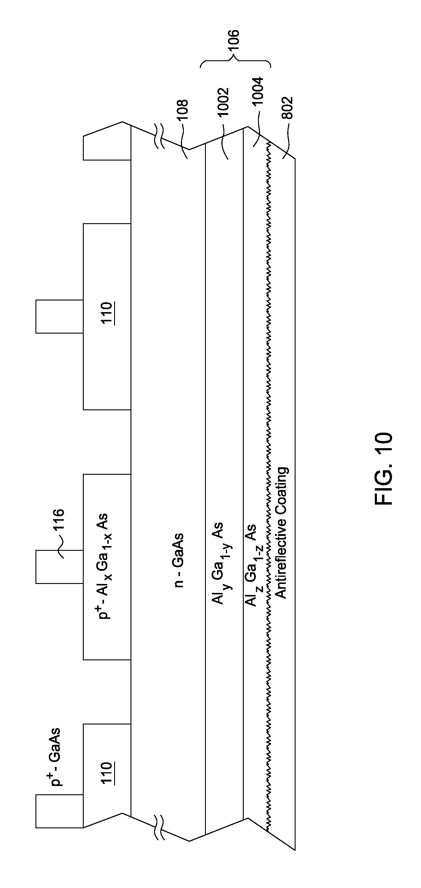
FIG. 10 illustrates multiple window layers, wherein the outermost window layer is roughened before the antireflective coating is applied, in accordance with an embodiment of the present invention.
FIG. 11 illustrates a roughened emitter layer on the back side of the PV unit, in accordance with an embodiment of the present invention.
FIG. 12 illustrates a diffuser on the back side of the PV unit, in accordance with an embodiment of the present invention.
FIG. 13 illustrates dielectric particles and white paint functioning as the diffuser of FIG. 12, in accordance with an embodiment of the present invention.
FIG. 14 illustrates metal particles functioning as the diffuser of FIG. 12, in accordance with an embodiment of the present invention.
FIG. 15A illustrates the back side of the PV unit, in accordance with an embodiment of the present invention.
FIG. 15B illustrates an equivalent electrical circuit of the PV unit of FIG. 15A, in accordance with an embodiment of the present invention.
FIG. 16 illustrates the interconnection of the p-contacts and of the n-contacts between the multiple PV units to form a PV bank, in accordance with an embodiment of the present invention.
FIG. 17 illustrates the interconnection of multiple PV banks to form a PV module, in accordance with an embodiment of the present invention.
DETAILED DESCRIPTION
Embodiments of the present invention provide techniques and apparatus for converting electromagnetic radiation, such as solar energy, into electric energy with increased efficiency when compared to conventional solar cells.
AN EXEMPLARY THIN ABSORBER LAYER
FIG. 1 illustrates various epitaxial layers of a photovoltaic (PV) unit 100 in cross-section during fabrication. The various layers may be formed using any suitable method for semiconductor growth, such as molecular beam epitaxy (MBE) or metalorganic chemical vapor deposition (MOCVD), on a substrate (not shown).
To form the PV unit 100, one or more buffer layers may be formed on the substrate. The purpose of the buffer layer(s) is to provide an intermediary between the substrate and the semiconductor layers of the final PV unit that can accommodate their different crystallographic structures as the various epitaxial layers are formed. Having a thickness of about 200 nm, for example, a buffer layer 102 may comprise a group III-V compound semiconductor, such as gallium arsenide (GaAs), depending on the desired composition of the final PV unit. For some embodiments, for example, the substrate may comprise GaAs when creating a GaAs buffer layer.
For some embodiments, a release layer 104 may be formed above the buffer layer 102. The release layer 104 may comprise aluminum arsenide (AlAs), for example, and have a thickness in a range from about 5 to 10 nm. The purpose of the thin release layer 104 is described in greater detail below.
Above the release layer 104, a window layer 106 may be formed. The window layer 106 may comprise aluminum gallium arsenide (AlGaAs), such as Al.sub.0.3Ga.sub.0.7As. The window layer 106 may have a thickness in a range of about 5 to 30 nm (e.g., 20 nm as shown) and may be undoped. The window layer 106 may be transparent to allow photons to pass through the window layer on the front side of the PV unit to other underlying layers.
A base layer 108 may be formed above the window layer 106. The base layer 108 may comprise any suitable group III-V compound semiconductor, such as GaAs. The base layer 108 may be monocrystalline. The base layer 108 may be n-doped, and for some embodiments, the doping concentration of the n-doped base layer 108 may be in a range from about 1.times.10.sup.16 to 1.times.10.sup.19 cm.sup.-3 (e.g., 2.times.10.sup.17 cm.sup.-3 as shown). The thickness of the base layer 108 may be in a range from about 300 to 3500 nm.
As illustrated in FIG. 1, an emitter layer 110 may be formed above the base layer 108. The emitter layer 110 may comprise any suitable group III-V compound semiconductor for forming a heterojunction with the base layer 108. For example, if the base layer 108 comprises GaAs, the emitter layer 110 may comprise a different semiconductor material, such as AlGaAs. If the emitter layer 110 and the window layer 106 both comprise AlGaAs, the Al.sub.xGa.sub.1-xAs composition of the emitter layer 110 may be the same as or different than the Al.sub.yGa.sub.1-yAs composition of the window layer 106. The emitter layer 110 may be monocrystalline. The emitter layer 110 may be heavily p-doped (i.e., p.sup.+-doped), and for some embodiments, the doping concentration of the p.sup.+-doped emitter layer may be in a range from about 1.times.10.sup.17 to 1.times.10.sup.20 cm.sup.-3 (e.g., 1.times.10.sup.19 cm.sup.-3 as shown). The thickness of the emitter layer 110 may be about 300 nm, for example. The combination of the base layer 108 and the emitter layer 110 may form an absorber layer for absorbing photons. For some embodiments, the absorber layer may have a thickness less than 800 nm, or even less than 500 nm.
The contact of an n-doped base layer to a p.sup.+-doped emitter layer creates a p-n layer 112. When light is absorbed near the p-n layer 112 to produce electron-hole pairs, the built-in electric field may force the holes to the p.sup.+-doped side and the electrons to the n-doped side. This displacement of free charges results in a voltage difference between the two layers 108, 110 such that electron current may flow when a load is connected across terminals coupled to these layers.
Rather than an n-doped base layer 108 and a p.sup.+-doped emitter layer 110 as described above, conventional photovoltaic semiconductor devices typically have a p-doped base layer and an n.sup.+-doped emitter layer. The base layer is typically p-doped in conventional devices due to the diffusion length of the carriers. Fabricating a thinner base layer according to embodiments of the invention allows for the change to an n-doped doped base layer. The higher mobility of electrons in an n-doped layer compared to the mobility of holes in a p-doped layer leads to the lower doping density in the n-doped base layer 108 of embodiments of the invention.
Once the emitter layer 110 has been formed, cavities or recesses 114 may be formed in the emitter layer deep enough to reach the underlying base layer 108. Such recesses 114 may be formed by applying a mask to the emitter layer 110 using photolithography, for example, and removing the semiconductor material in the emitter layer 110 not covered by the mask using any suitable technique, such as wet or dry etching. In this manner, the base layer 108 may be accessed via the back side of the PV unit 100.
For some embodiments, an interface layer 116 may be formed above the emitter layer 110. The interface layer 116 may comprise any suitable group III-V compound semiconductor, such as GaAs. The interface layer 116 may be p.sup.+-doped, and for some embodiments, the doping concentration of the p.sup.+-doped interface layer 116 may be 1.times.10.sup.19 cm.sup.-3. The thickness of the interface layer 116 may be about 300 nm, for example.
Once the remaining epitaxial layers have been formed above the release layer 104, the thin release layer 104 may be sacrificed via etching with aqueous HF, for example. In this manner, the functional layers of the PV unit 100 (e.g., the window layer 106, the base layer 108, and the emitter layer 110) may be separated from the buffer layer(s) 102 and substrate during the epitaxial lift-off (ELO) process.
A PV unit created in this manner has a significantly thin absorber layer (e.g., <500 nm) compared to conventional solar units, which may be several micrometers thick. The thickness of the absorber layer is proportional to dark current levels in the PV unit (i.e., the thinner the absorber layer, the lower the dark current). Dark current is the small electric current that flows through the PV unit or other similar photosensitive device (e.g., a photodiode) even when no photons are entering the device. This background current may be present as the result of thermionic emission or other effects. Because the open circuit voltage (V.sub.oc) increases as the dark current is decreased in a photosensitive semiconductor device, a thinner absorber layer may most likely lead to a greater V.sub.oc for a given light intensity and, thus, increased efficiency. As long as the absorber layer is able to trap light, the efficiency increases as the thickness of the absorber layer is decreased.
The thinness of the absorber layer may not only be limited by the capabilities of thin film technology and ELO. For example, efficiency increases with the thinness of the absorber layer, but the absorber layer should be thick enough to carry current. However, higher doping levels may allow current to flow, even in very thin absorber layers. Therefore, increased doping may be utilized to fabricate very thin absorber layers with even greater efficiency. Conventional PV devices may suffer from volume recombination effects, and therefore, such conventional devices do not employ high doping in the absorber layer. The sheet resistance of the absorber layer may also be taken into consideration when determining the appropriate thickness.
Not only does a thin absorber layer lead to increased efficiency, but PV units with such a thin absorber layer may be more flexible than conventional solar cells having a thickness of several micrometers. Therefore, PV units according to embodiments of the invention may be appropriate for a greater number of applications than conventional solar cells.
FIGS. 2A-D illustrate various layer stack profiles 200.sub.a-d for the base and emitter layers 108, 110 of the PV unit, in accordance with embodiments of the present invention. The layer stack profile 200.sub.a in FIG. 2A illustrates the base and emitter layers 108, 110 as illustrated in FIG. 1. For some embodiments, an intermediate layer 202 may be formed above the base layer 108, and the emitter layer 110 may be formed above the intermediate layer. The intermediate layer 202 may provide a more gradual transition between the base and emitter layers 108, 110.
The intermediate layer 202 may be n-doped, heavily n-doped (i.e., n.sup.+-doped), or p.sup.+-doped. For example, FIG. 2B illustrates an intermediate layer 202.sub.b comprising n-AlGaAs. As another example, FIG. 2C depicts an intermediate layer 202.sub.c comprising n.sup.+-AlGaAs. As yet another example, FIG. 2D portrays an intermediate layer 202.sub.d comprising p.sup.+-GaAs.
In FIG. 1, the p-n layer 112 between the base layer 108 and the emitter layer 110 is flat and is not exposed in the recesses 114. In other words, the p-n layer 112 of FIG. 1 may be considered as a plane having only two-dimensional geometry. For some embodiments, as shown in FIGS. 3A and 3B, the semiconductor layers for a PV unit may be formed to create an offset p-n layer 312 between the base and emitter layers 108, 110. In other words, an offset p-n layer 312 may be considered to have three-dimensional geometry. An offset p-n layer 312 may be exposed in the recesses 114.
As illustrated in FIG. 3A, an offset p-n layer 312.sub.a may be produced by removing semiconductor material all the way through the emitter layer 110 and partially into the base layer 108 when forming the recesses 114 as described above. Another method of forming an offset p-n layer 312.sub.b, as illustrated in FIG. 3B, may comprise applying a mask to the base layer 108 before forming the emitter layer 110. Semiconductor material may be removed via any suitable technique, such as etching, from a portion of the base layer 108 where the emitter layer is intended to remain (i.e., everywhere except the desired locations of the recesses 114). Once the emitter layer 110 and the recesses 114 are formed in the emitter layer, the resulting offset p-n layer 312.sub.b has a greater surface area than a flat p-n layer 112.
For some embodiments, doping levels may be fine-tuned within a layer of the PV unit during fabrication. For example, FIG. 4 illustrates a PV unit 400 with an emitter layer 110 having a doping profile fine-tuned such that the doping concentration increases from the p-n layer 112 to the top of the emitter layer 110 in the z-direction.
For some embodiments, the emitter layer 110 may comprise multiple layers, and the multiple layers may comprise different compositions. For example, FIG. 5 illustrates semiconductor layers for a PV unit 500 with multiple p.sup.+-AlGaAs emitter layers having graded aluminum (Al) levels (i.e., percentages), in accordance with an embodiment of the present invention. In this example embodiment, a first emitter layer 510.sub.1 comprising p.sup.+-GaAs without any aluminum may be formed above the base layer 108. A second emitter layer 510.sub.2 comprising p.sup.+-Al.sub.0.1Ga.sub.0.3As may be formed above the first emitter layer 510.sub.1. Then, a third emitter layer 510.sub.3 comprising p.sup.+-Al.sub.0.2Ga.sub.0.8As and a fourth emitter layer 510.sub.4 comprising p.sup.+-Al.sub.0.3Ga.sub.0.7As may be formed above the second emitter layer 510.sub.2, in turn. Having such graded Al levels may avoid junction barriers.
Exemplary Electrical Contacts
Electrical contacts may be used to couple the semiconductor layers of the PV unit 100 to wires for connection to other PV units and for external connection to a load. A conventional solar cell typically has contacts on both the front and back sides of the cell. Front side contacts, especially thicker ones, create shadows where light cannot reach the underlying absorber layer to be converted into electric energy. Therefore, the efficiency potential of the solar cell cannot be obtained. Accordingly, techniques and apparatus for contacting the semiconductor layers of the PV unit without introducing shadows are needed.
FIG. 6 illustrates all electrical contacts to the semiconductor layers being on the back side of the PV unit 100, according to an embodiment of the present invention. For example, n-contacts 602 may be formed in the recesses 114 to provide an interface to the n-doped base layer 108, and p-contacts 604 may be formed above the interface layer 116 to couple to the p.sup.+-doped emitter layer 110. The heavy doping in the p.sup.+-doped interface layer 116 may facilitate making an ohmic contact. In this manner, efficiency need not be sacrificed by having electrical contacts on the front side of the PV unit to block light and create solar shadows.
The pattern of the recesses 114 in the emitter layer 110 and the remaining portion of the interface layer 116 for the contacts 602, 604 may be based on the desired sheet resistance. The dimensions (e.g., area) of the contacts 602, 604 may be very small compared to the dimensions (e.g., area) of a single PV unit 100. What is more, the pattern of the contacts 602, 604 may provide a built-in tolerance against local defects and shadowing.
The contacts 602, 604 may comprise any suitable electrically conductive material, such as a metal or a metal alloy. Preferably, the material for the contacts should not punch through the semiconductor layers during fabrication. Traditional contacts comprising gold (Au) often had this spiking problem. Furthermore, the material for the back side contacts may preferably be capable of being applied at relatively low metallization process temperatures, such as between 150 and 200.degree. C. For example, the contact 602, 604 may comprise palladium/germanium (Pd/Ge) to meet these design goals. Palladium does not react with GaAs.
Whatever material is selected, the contacts 602, 604 may be fabricated on the PV unit 100 by any suitable method, such as vacuum-evaporation through a photoresist, photolithography, screen printing, or merely depositing on the exposed portion of the PV units that have been partially covered with wax or another protective material. These methods all involve a system in which the part of the PV unit on which a contact is not desired is protected, while the rest of the PV unit is exposed to the metal. Of these, screen printing may be the most cost effective, helping to decrease the cost of the resulting PV devices.
Despite all the contacts 602, 604 being on the back side of the PV unit 100 to reduce solar shadows, dark current and its stability with time and temperature may still be concerns when designing an efficient PV unit. An exposed p-n layer 112 may be a source of dark current, and larger recesses 114 may be responsible for an increase in dark current. Thus, smaller recesses 114 may be desired. However, there is a tradeoff between reducing the size of the recesses 14 to reduce dark current and the probability of fabricating the n-contacts 602 in the recesses 114 without touching the sidewalls.
Therefore, for some embodiments, the sidewalls of the recesses 114 may be passivated as another way to reduce the dark current in the PV unit. FIG. 7 illustrates passivation 702 on the sidewalls (i.e., lateral surfaces) of the recesses 114 in the emitter layer 110, in accordance with an embodiment of the present invention. The sidewalls may be passivated most likely before--but possibly after--the n-contacts 602 are formed, using any suitable passivation method, such as chemical vapor deposition (CVD) or plasma-enhanced CVD (PECVD). The passivation 702 may comprise any suitable electrically non-conductive material, such as silicon nitride (SiN), SiO.sub.x, TiO.sub.x, TaO.sub.x, zinc sulfide (ZnS), or any combination thereof.
Exemplary Light Trapping
To achieve efficiency, the absorber layer of an ideal photovoltaic (PV) device would absorb all of the photons impinging on the PV device's front side facing the light source since the open circuit voltage (V.sub.oc) or short circuit current (I.sub.sc) is proportional to the light intensity. However, several loss mechanisms typically interfere with the PV device's absorber layer seeing or absorbing all of the light reaching the front side of the device. For example, the semiconductor layers of the PV device may be shiny (especially when made of pure silicon) and, therefore, may reflect a substantial portion of the impinging photons, preventing these photons from ever reaching the absorber layer. If two semiconductor layers (e.g., the window layer and the base layer) have a different index of refraction, some of the photons reaching the interface between these two layers may be reflected according to Snell's Law if their angle of incidence is too high, again preventing these photons from reaching the absorber layer. Furthermore, the absorber layer may not absorb all of the impinging photons; some photons may pass through the absorber layer without affecting any electron-hole pairs.
Accordingly, there is a need for techniques and apparatus to capture the light impinging on the front side of the PV device such that as many photons as possible may be absorbed by the absorber layer and converted into electric energy. In this manner, the PV device's efficiency may be increased.
Apparatus for trapping the light within the semiconductor layers of a PV device may be divided into two categories: front side light trapping and back side light trapping. By employing both types of light trapping in a PV device, the idea is that nearly all photons impinging on the PV device's front side may be captured and "bounce around" within the semiconductor layers until the photons are absorbed by the absorber layer and converted to electric energy.
Exemplary Front Side Light Trapping
FIG. 8 illustrates an antireflective (AR) coating 802 disposed adjacent to the window layer 106 on the front side of the PV unit 100, in accordance with an embodiment of the present invention. According to its purpose, the AR coating 802 may comprise any suitable material that allows light to pass through while preventing light reflection from its surface. For example, the AR coating 802 may comprise magnesium fluoride (MgF.sub.2), zinc sulfide (ZnS), silicon nitride (SiN), titanium dioxide (TiO.sub.2), silicon dioxide (SiO.sub.2), or any combination thereof. The AR coating 802 may be applied to the window layer 106 by any suitable technique, such as sputtering.
For some embodiments, the window layer 106 may be roughened or textured before applying the antireflective coating 802. FIG. 9 illustrates a roughened window layer 106. Roughening of the window layer 106 may be accomplished by wet etching or dry etching, for example. Texturing may be achieved by applying small particles, such as polystyrene spheres, to the surface of the window layer 106 before applying the AR coating 802. By roughening or texturing the window layer 106, different angles are provided at the interface between the AR coating 802 and the window layer, which may have different indices of refraction. In this manner, more of the incident photons may be transmitted into the window layer 106 rather than reflected from the interface between the AR coating 802 and the window layer because some photons' angles of incidence are too high according to Snell's Law. Thus, roughening or texturing the window layer 106 may provide increased light trapping.
Also for some embodiments, the window layer 106 may comprise multiple window layers. For these embodiments, the outermost window layer (i.e., the window layer closest to the front side of the PV unit 100) may be roughened or textured as described above before the antireflective coating 802 is applied, as illustrated in FIG. 10. In FIG. 10, the window layer 106 comprises a first window layer 1002 disposed adjacent to the base layer 108 and a second window layer 1004 interposed between the first window layer 1002 and the antireflective coating 802. The first and second window layers 1002, 1004 may comprise any material suitable for the window layer 106 as described above, such as AlGaAs, but typically with different compositions. For example, the first window layer 1002 may comprise Al.sub.0.3Ga.sub.0.7As, and the second window layer 1004 may comprise Al.sub.0.1Ga.sub.0.9As. Furthermore, some of the multiple window layers may be doped, while others are undoped for some embodiments. For example, the first window layer 1002 may be doped, and the second window layer 1004 may be undoped.
Exemplary Back Side Light Trapping
For some embodiments, the emitter layer 110 on the back side of the PV unit 100 may be roughened or textured, as described above with respect to the front side, in an effort to increase light trapping. FIG. 11 illustrates such a roughened emitter layer 110.
FIG. 12 illustrates a diffuser 1202 on the back side of the PV unit 100 in an effort to increase the amount of light captured by the absorber layer. Rather than reflecting photons similar to a mirror where the angle of reflectance equals the angle of incidence, the purpose of the diffuser 1202 is to diffuse or scatter photons that pass through the absorber layer without being absorbed. For some embodiments, the diffuser 1202 may be covered with a reflective layer 1204. In this manner, the diffuser 1202 may provide new angles to incident photons, some of which may be redirected back to the interior of the PV unit. For other photons that are directed to the back side of the PV unit, the reflective layer 1204 may redirect these photons back through the diffuser 1202 and towards the interior of the PV unit. Although some of the light may be absorbed by the diffuser 1202 as the photons are scattered and redirected inside, much of the light is redirected to the absorber layer to be absorbed and converted into electric energy, thereby increasing efficiency. Conventional PV devices without a diffuser and a reflective layer may not be able to recapture photons that reach the back side of the device without being absorbed initially by the absorber layer.
For some embodiments, the diffuser 1202 may comprise dielectric particles 1302, as illustrated in FIG. 13. The dielectric particles may comprise any suitable material which is electrically insulative and does not absorb light. The dielectric particles 1302 may have a diameter in range from about 0.2 to 2.0 .mu.m. The dielectric particles 1302 may be covered by white paint 1304, which reflects light and may act as the reflective layer for redirecting photons back to the interior of the PV unit 100. The white paint 1304 may comprise TiO.sub.2, for example.
For some embodiments, the diffuser 1202 may comprise metal particles 1402, as illustrated in FIG. 14. The metal particles 1402 may reflect photons that were not absorbed by the absorber layer, and by having a multitude of metal particles 1402, the photons may be scattered in different directions several times before being redirected to the interior of the PV unit 100. The metal particles 1402 may have a diameter of about 150 to 200 nm, functioning as relatively compact scatterers. With thinner particles in the diffuser 1202, the thickness of the PV unit 100 may be kept smaller, thereby maintaining the desired flexibility of the PV unit 100.
Because the metal particles 1402 are electrically conductive, lateral surfaces of the interface layer 116 may be passivated to prevent the metal particles 1402 from interfering with the operation of the device. The interface layer 116 may be passivated using any suitable passivation method, such as chemical vapor deposition (CVD) or plasma-enhanced CVD (PECVD). The passivation 1404 may comprise any suitable electrically non-conductive material, such as silicon nitride (SiN), SiO.sub.x, TiO.sub.x, TaO.sub.x, zinc sulfide (ZnS), or any combination thereof. Furthermore, for some embodiments, a dielectric layer 1406 may be formed above the metal particles 1402 in an effort to avoid shunting the contacts 602, 604, as depicted in FIG. 14. The dielectric layer 1406 may comprise any suitable electrically insulative material, such as SiO.sub.2, SiN, or glass.
Exemplary Integration
FIG. 15A illustrates the back side of the PV unit 100, wherein all the contacts 602, 604 are disposed on the back side. As described above, the n-contacts 602 may be located within the recesses 114 in the emitter layer 110. The PV unit 100 may have a width w of about 2 to 3 cm and a length/of about 10 cm.
FIG. 15B illustrates an equivalent electrical circuit 1500 of the PV unit 100 of FIG. 15A. One may consider the PV unit 100 as having an efficient miniature solar cell 1502 between each n-contact 602 and p-contact 604. Within a PV unit 100, all of the n-contacts 602 are coupled to the same base layer 108 and all of the p-contacts 604 are coupled to the same emitter layer 110. Therefore, the open circuit voltage (V.sub.oc) of the equivalent circuit 1500 may be modeled as the sum of the open circuit voltages across the miniature solar cells 1502 in series, and the short circuit current (I.sub.sc) may be modeled as the sum of the short circuit currents across the miniature solar cells 1502 in parallel. In essence, the equivalent electrical circuit 1500 of the PV unit 100 may be thought of as a single solar cell with a greater V.sub.oc and a larger I.sub.sc than those of the miniature solar cells 1502 which compose it.
FIG. 16 illustrates the interconnection of the p-contacts 604 and of the n-contacts between multiple PV units 100 to form a PV bank 1600, in accordance with an embodiment of the present invention. For some embodiments, a PV bank 1600 may comprise one column of about ten PV units 100 arranged in parallel. In this manner, the short circuit current (I.sub.sc) of the PV bank 1600 may be about ten times greater than that of a single PV unit 100.
The interconnection may be accomplished by thin strips 1602, 1604 placed between the PV units 100 according to a certain pattern. For example, strips 1604 may connect the p-contacts 604 of a first PV unit 100.sub.1 to the p-contacts 604 of a second PV unit 100.sub.2. Rather than connecting the first PV unit 100.sub.1 to the second PV unit 100.sub.2 for the n-contacts, strips 1602 may connect the n-contacts 602 of the second PV unit 100.sub.2 to the n-contacts 602 of a third PV unit 100.sub.3 as illustrated in FIG. 16. This interconnection pattern may be selected to provide considerable flexibility in the PV bank 1600.
The strips 1602, 1604 may comprise any suitable electrically conductive material, such as metal or metal alloys. For example, the strips 1602, 1604 may comprise tin-coated copper. For some embodiments, the strips 1602 for the n-contacts may comprise a different material than the strips 1604 for the p-contacts 604. To form strips made of metal or metal alloys, the strips may be applied to the back side of the PV units 100 across the "dot geometry" of the contacts 602, 604 via screen printing, for example.
Screen printing metals or metal alloys may indicate a high process temperature. Therefore, for some embodiments, the strips 1602, 1604 may comprise an electrically conductive polymer instead of a metal or metal alloy. The conductive polymer strips may be formed by screen printing at a lower temperature than that suggested by silk-screening metal.
The spacing between adjacent PV units 100 may be about 1 to 2 mm on the PV bank 1600. This relatively close spacing may also allow for greater flexibility in the PV bank 1600, especially when combined with an interconnection pattern selected for this purpose, such as the interconnection pattern described above.
FIG. 17 illustrates the interconnection of multiple PV banks 1600 arranged in an array to form a PV module 1700, in accordance with an embodiment of the present invention. Adjacent PV banks 1600 in a row may be connected together by couplings 1702. The couplings 1702 may connect the n-contact 602 of one PV bank to the p-contact 604 of an adjacent PV bank within the row, such that the PV banks 1600 (and the equivalent electric circuit) of a row are connected in series, thereby combining the open circuit voltage (V.sub.oc) capabilities of the PV banks 1600. The couplings 1702 may comprise a wire or a strip of metal, metal alloy, or a conductive polymer, similar to the strips 1602, 1604 in the PV banks 1600.
The couplings 1702 may also connect a p-contact 604 on each row of PV banks 1600 to a p-side bus-bar 1704 on one side and connect an n-contact 602 on each row of PV banks 1600 to an n-side bus-bar 1706 on the other side of the PV module 1700. In this manner, the rows of series-connected PV banks 1600 may be connected in parallel, thereby combining the short circuit current (I.sub.sc) capabilities of the PV banks 1600. The bus-bars 1704, 1706 may be relatively thick in an effort to carry substantial current generated by the PV banks 1600 to a load (not shown). For some embodiments, the DC output voltage (V.sub.oc) of the module 1700 may be coupled to an inverter in an effort to create AC voltage.
The finished PV module 1700 may be encapsulated. The front side of the PV module 1700 may be covered with a thin transparent sheet comprising glass or plastic, for example. The length L of the module may be about 1 m with a 4.times.4 array of PV banks 1600 as illustrated in FIG. 16.
By connecting the PV units 100 with the strips 1602, 1604 to form PV banks 1600 and by integrating the PV banks 1600 with couplings 1702 to develop the PV module 1700, the PV module 1700 may have a built-in tolerance against local defects. In other words, a defect (e.g., a shunt between an n-contact 602 and a p-contact 604) localized to a PV unit 100 need not cause the module 1700 to fail. Furthermore, protection may be added at the macroscopic and/or the microscopic level. In other words, protection, such as fuses, may be added to one or more PV banks 1600 and/or to the PV module 1700. For some embodiments, protection circuitry may be built into the PV units 100 at the wafer level.
While the foregoing is directed to embodiments of the invention, other and further embodiments of the invention may be devised without departing from the basic scope thereof, and the scope thereof is determined by the claims that follow.
* * * * *
References
D00000
D00001
D00002
D00003
D00004
D00005
D00006
D00007
D00008
D00009
D00010
D00011
D00012

D00013

D00014

D00015

D00016

D00017

D00018

XML
uspto.report is an independent third-party trademark research tool that is not affiliated, endorsed, or sponsored by the United States Patent and Trademark Office (USPTO) or any other governmental organization. The information provided by uspto.report is based on publicly available data at the time of writing and is intended for informational purposes only.
While we strive to provide accurate and up-to-date information, we do not guarantee the accuracy, completeness, reliability, or suitability of the information displayed on this site. The use of this site is at your own risk. Any reliance you place on such information is therefore strictly at your own risk.
All official trademark data, including owner information, should be verified by visiting the official USPTO website at www.uspto.gov. This site is not intended to replace professional legal advice and should not be used as a substitute for consulting with a legal professional who is knowledgeable about trademark law.