Switching in an audio system with multiple playback paths
Das , et al.
U.S. patent number 10,321,230 [Application Number 15/482,250] was granted by the patent office on 2019-06-11 for switching in an audio system with multiple playback paths. This patent grant is currently assigned to Cirrus Logic, Inc.. The grantee listed for this patent is Cirrus Logic International Semiconductor Ltd.. Invention is credited to Tejasvi Das, Xiaofan Fei, Ku He, Xin Zhao.


| United States Patent | 10,321,230 |
| Das , et al. | June 11, 2019 |
Switching in an audio system with multiple playback paths
Abstract
In accordance with embodiments of the present disclosure, a system may include a playback path and a control circuit. The playback path may have a playback input for receiving an input signal and configured to generate at a playback path output an output signal based on the input signal, wherein the playback path is configured to operate in a plurality of operational modes. The control circuit may be configured to receive a first signal from within the playback path and indicative of the input signal, receive a second signal generated from the input signal externally to the playback path, and select a selected operational mode from the plurality of operational modes based on the first signal and the second signal.
| Inventors: | Das; Tejasvi (Austin, TX), Zhao; Xin (Austin, TX), He; Ku (Austin, TX), Fei; Xiaofan (Austin, TX) | ||||||||||
|---|---|---|---|---|---|---|---|---|---|---|---|
| Applicant: |
|
||||||||||
| Assignee: | Cirrus Logic, Inc. (Austin,
TX) |
||||||||||
| Family ID: | 59010976 | ||||||||||
| Appl. No.: | 15/482,250 | ||||||||||
| Filed: | April 7, 2017 |
Prior Publication Data
| Document Identifier | Publication Date | |
|---|---|---|
| US 20180295442 A1 | Oct 11, 2018 | |
| Current U.S. Class: | 1/1 |
| Current CPC Class: | H03F 1/0277 (20130101); H03F 3/211 (20130101); H03F 3/217 (20130101); H03F 3/2178 (20130101); H03F 3/185 (20130101); H03F 3/30 (20130101); H04R 29/00 (20130101); H04R 3/00 (20130101); H03F 3/72 (20130101); H03F 2200/03 (20130101); H03F 2200/411 (20130101); H03F 2200/432 (20130101); H04R 2420/03 (20130101) |
| Current International Class: | H04R 3/00 (20060101); H03F 99/00 (20090101); H03F 1/02 (20060101); H03F 3/21 (20060101); H03F 3/217 (20060101); H03F 3/30 (20060101); H03F 3/72 (20060101); H03F 3/185 (20060101); H04R 29/00 (20060101) |
References Cited [Referenced By]
U.S. Patent Documents
| 3683164 | August 1972 | Minami |
| 4346349 | August 1982 | Yokoyama |
| 4441081 | April 1984 | Jenkins |
| 4446440 | May 1984 | Bell |
| 4493091 | January 1985 | Gundry |
| 4628526 | December 1986 | Germer |
| 4890107 | December 1989 | Pearce |
| 4972436 | November 1990 | Halim et al. |
| 4999628 | March 1991 | Kakaubo et al. |
| 4999830 | March 1991 | Agazzi |
| 5077539 | December 1991 | Howatt |
| 5148167 | September 1992 | Ribner |
| 5198814 | March 1993 | Ogawara et al. |
| 5212551 | May 1993 | Conanan |
| 5272449 | December 1993 | Izawa |
| 5321758 | June 1994 | Charpentier et al. |
| 5323159 | June 1994 | Imamura et al. |
| 5343161 | August 1994 | Tokumo et al. |
| 5434560 | July 1995 | King et al. |
| 5495505 | February 1996 | Kundmann |
| 5550923 | July 1996 | Hotvet et al. |
| 5600317 | February 1997 | Knoth et al. |
| 5714956 | February 1998 | Jahne et al. |
| 5719641 | February 1998 | Mizoguchi |
| 5771301 | June 1998 | Fuller et al. |
| 5796303 | August 1998 | Vinn et al. |
| 5808575 | September 1998 | Himeno et al. |
| 5810477 | September 1998 | Abraham et al. |
| 6088461 | July 2000 | Lin |
| 6160455 | December 2000 | French et al. |
| 6201490 | March 2001 | Kawano et al. |
| 6260176 | July 2001 | Chen |
| 6271780 | August 2001 | Gong et al. |
| 6333707 | December 2001 | Oberhammer et al. |
| 6353404 | March 2002 | Kuroiwa |
| 6542612 | April 2003 | Needham |
| 6614297 | September 2003 | Score |
| 6683494 | January 2004 | Stanley |
| 6745355 | June 2004 | Tamura |
| 6768443 | July 2004 | Willis |
| 6810266 | October 2004 | Ecklund et al. |
| 6822595 | November 2004 | Robinson |
| 6853242 | February 2005 | Melanson et al. |
| 6888888 | May 2005 | Tu et al. |
| 6897794 | May 2005 | Kuyel et al. |
| 6989955 | January 2006 | Ziemer et al. |
| 7020892 | March 2006 | Levesque et al. |
| 7023268 | April 2006 | Taylor et al. |
| 7061312 | June 2006 | Andersen et al. |
| 7167112 | January 2007 | Andersen et al. |
| 7216249 | May 2007 | Fujiwara et al. |
| 7279964 | October 2007 | Bolz et al. |
| 7302354 | November 2007 | Zhuge |
| 7312734 | December 2007 | McNeill et al. |
| 7315204 | January 2008 | Seven |
| 7365664 | April 2008 | Caduff et al. |
| 7378902 | May 2008 | Sorrells et al. |
| 7385443 | June 2008 | Denison |
| 7403010 | July 2008 | Hertz |
| 7440891 | October 2008 | Shozakai et al. |
| 7522677 | April 2009 | Liang |
| 7583215 | September 2009 | Yamamoto et al. |
| 7671768 | March 2010 | De Ceuninck |
| 7679538 | March 2010 | Tsang |
| 7733592 | June 2010 | Hutchins et al. |
| 7737776 | June 2010 | Cyrusian |
| 7893856 | February 2011 | Ek et al. |
| 7924189 | April 2011 | Sayers |
| 7937106 | May 2011 | Sorrells et al. |
| 7952502 | May 2011 | Kolze et al. |
| 8060663 | November 2011 | Murray et al. |
| 8130126 | March 2012 | Breitschaedel et al. |
| 8194889 | June 2012 | Seefeldt |
| 8298425 | October 2012 | Kanbe |
| 8330631 | December 2012 | Kumar et al. |
| 8362936 | January 2013 | Ledzius et al. |
| 8462035 | June 2013 | Schimper et al. |
| 8483753 | July 2013 | Behzad et al. |
| 8508397 | August 2013 | Hisch |
| 8717211 | May 2014 | Miao et al. |
| 8786477 | July 2014 | Albinet |
| 8836551 | September 2014 | Nozaki |
| 8873182 | October 2014 | Liao et al. |
| 8878708 | November 2014 | Sanders et al. |
| 8952837 | February 2015 | Kim et al. |
| 9071201 | June 2015 | Jones et al. |
| 9071267 | June 2015 | Schneider et al. |
| 9071268 | June 2015 | Schneider et al. |
| 9118401 | August 2015 | Nieto et al. |
| 9148164 | September 2015 | Schneider et al. |
| 9171552 | October 2015 | Yang |
| 9178462 | November 2015 | Kurosawa et al. |
| 9210506 | December 2015 | Nawfal et al. |
| 9306588 | April 2016 | Das et al. |
| 9337795 | May 2016 | Das et al. |
| 9391576 | July 2016 | Satoskar et al. |
| 9444504 | September 2016 | Robinson et al. |
| 9503027 | November 2016 | Zanbaghi |
| 9525940 | December 2016 | Schneider et al. |
| 9543975 | January 2017 | Melanson et al. |
| 9584911 | February 2017 | Das et al. |
| 9596537 | March 2017 | He et al. |
| 9635310 | April 2017 | Chang et al. |
| 9680488 | June 2017 | Das et al. |
| 9762255 | September 2017 | Satoskar et al. |
| 9774342 | September 2017 | Schneider et al. |
| 9780800 | October 2017 | Satoskar et al. |
| 9807504 | October 2017 | Melanson et al. |
| 9813814 | November 2017 | Satoskar |
| 9831843 | November 2017 | Das et al. |
| 9917557 | March 2018 | Zhu et al. |
| 9929703 | March 2018 | Zhao |
| 2001/0001547 | May 2001 | Delano et al. |
| 2001/0009565 | July 2001 | Singvall |
| 2004/0078200 | April 2004 | Alves |
| 2004/0184621 | September 2004 | Andersen et al. |
| 2005/0068097 | March 2005 | Kirn et al. |
| 2005/0084037 | April 2005 | Liang |
| 2005/0258989 | November 2005 | Li et al. |
| 2005/0276359 | December 2005 | Xiong |
| 2006/0056491 | March 2006 | Lim et al. |
| 2006/0064037 | March 2006 | Shalon et al. |
| 2006/0098827 | May 2006 | Paddock et al. |
| 2006/0261886 | November 2006 | Hansen et al. |
| 2006/0284675 | December 2006 | Krochmal et al. |
| 2007/0018719 | January 2007 | Seven |
| 2007/0026837 | February 2007 | Bagchi |
| 2007/0057720 | March 2007 | Hand et al. |
| 2007/0092089 | April 2007 | Seefeldt et al. |
| 2007/0103355 | May 2007 | Yamada |
| 2007/0120721 | May 2007 | Caduff et al. |
| 2007/0123184 | May 2007 | Nesimoglu et al. |
| 2007/0142943 | June 2007 | Torrini et al. |
| 2007/0146069 | June 2007 | Wu |
| 2008/0012639 | January 2008 | Mels |
| 2008/0030577 | February 2008 | Cleary et al. |
| 2008/0114239 | May 2008 | Randall et al. |
| 2008/0143436 | June 2008 | Xu |
| 2008/0159444 | July 2008 | Terada |
| 2008/0198048 | August 2008 | Klein et al. |
| 2008/0278632 | November 2008 | Morimoto |
| 2008/0292107 | November 2008 | Bizjak |
| 2009/0015327 | January 2009 | Wu |
| 2009/0021643 | January 2009 | Hsueh et al. |
| 2009/0051423 | February 2009 | Miaille |
| 2009/0058531 | March 2009 | Hwang et al. |
| 2009/0084586 | April 2009 | Nielsen |
| 2009/0220110 | September 2009 | Bazarjani et al. |
| 2010/0168882 | July 2010 | Zhang et al. |
| 2010/0176980 | July 2010 | Breitschadel et al. |
| 2010/0183163 | July 2010 | Matsui et al. |
| 2010/0195771 | August 2010 | Takahashi |
| 2011/0013733 | January 2011 | Martens et al. |
| 2011/0025540 | February 2011 | Katsis |
| 2011/0029109 | February 2011 | Thomsen et al. |
| 2011/0044414 | February 2011 | Li |
| 2011/0063148 | March 2011 | Kolze et al. |
| 2011/0096370 | April 2011 | Okamoto |
| 2011/0136455 | June 2011 | Sundstrom et al. |
| 2011/0150240 | June 2011 | Akiyama et al. |
| 2011/0170709 | July 2011 | Guthrie et al. |
| 2011/0188671 | August 2011 | Anderson et al. |
| 2011/0228952 | September 2011 | Lin |
| 2011/0242614 | October 2011 | Okada |
| 2011/0268301 | November 2011 | Nielsen et al. |
| 2011/0285463 | November 2011 | Walker et al. |
| 2012/0001786 | January 2012 | Hisch |
| 2012/0007757 | January 2012 | Choe et al. |
| 2012/0047535 | February 2012 | Bennett et al. |
| 2012/0133411 | May 2012 | Miao et al. |
| 2012/0177201 | July 2012 | Ayling et al. |
| 2012/0177226 | July 2012 | Silverstein et al. |
| 2012/0188111 | July 2012 | Ledzius et al. |
| 2012/0207315 | August 2012 | Kimura et al. |
| 2012/0242521 | September 2012 | Kinyua |
| 2012/0250893 | October 2012 | Carroll et al. |
| 2012/0263090 | October 2012 | Porat et al. |
| 2012/0274490 | November 2012 | Kidambi et al. |
| 2012/0280726 | November 2012 | Colombo et al. |
| 2012/0293348 | November 2012 | Snelgrove |
| 2012/0314750 | December 2012 | Mehrabani |
| 2013/0095870 | April 2013 | Phillips et al. |
| 2013/0106635 | May 2013 | Doi |
| 2013/0129117 | May 2013 | Thomsen et al. |
| 2013/0188808 | July 2013 | Pereira et al. |
| 2013/0235484 | September 2013 | Liao et al. |
| 2013/0241753 | September 2013 | Nozaki |
| 2013/0241755 | September 2013 | Chen et al. |
| 2014/0044280 | February 2014 | Jiang |
| 2014/0105256 | April 2014 | Hanevich et al. |
| 2014/0105273 | April 2014 | Chen et al. |
| 2014/0126747 | May 2014 | Huang |
| 2014/0135077 | May 2014 | Leviant et al. |
| 2014/0184332 | July 2014 | Shi et al. |
| 2014/0269118 | September 2014 | Taylor et al. |
| 2014/0363023 | December 2014 | Li et al. |
| 2014/0368364 | December 2014 | Hsu |
| 2015/0009079 | January 2015 | Bojer |
| 2015/0170663 | June 2015 | Disch et al. |
| 2015/0214974 | July 2015 | Currivan |
| 2015/0214975 | July 2015 | Gomez et al. |
| 2015/0249466 | September 2015 | Elyada |
| 2015/0295584 | October 2015 | Das et al. |
| 2015/0327174 | November 2015 | Rajagopal et al. |
| 2015/0381130 | December 2015 | Das et al. |
| 2016/0072465 | March 2016 | Das et al. |
| 2016/0080862 | March 2016 | He et al. |
| 2016/0080865 | March 2016 | He et al. |
| 2016/0139230 | May 2016 | Petrie et al. |
| 2016/0173112 | June 2016 | Das et al. |
| 2016/0181988 | June 2016 | Du et al. |
| 2016/0286310 | September 2016 | Das et al. |
| 2016/0365081 | December 2016 | Satoskar et al. |
| 2017/0047895 | February 2017 | Zanbaghi |
| 2017/0150257 | May 2017 | Das et al. |
| 2017/0212721 | July 2017 | Satoskar et al. |
| 2017/0374459 | December 2017 | Satoskar |
| 2018/0046239 | February 2018 | Schneider |
| 2018/0048325 | February 2018 | Schneider |
| 2018/0098149 | April 2018 | Das |
| 3351788 | Jul 1989 | EP | |||
| 0966105 | Dec 1999 | EP | |||
| 1244218 | Sep 2002 | EP | |||
| 1575164 | Sep 2005 | EP | |||
| 1689075 | Aug 2006 | EP | |||
| 1753130 | Feb 2007 | EP | |||
| 1798852 | Jun 2009 | EP | |||
| 2207264 | Jul 2010 | EP | |||
| 1599401 | Sep 1981 | GB | |||
| 2119189 | Nov 1983 | GB | |||
| 2307121 | Jun 1997 | GB | |||
| 2507096 | Apr 2014 | GB | |||
| 2527637 | Dec 2015 | GB | |||
| 2527677 | Oct 2016 | GB | |||
| 2537694 | Oct 2016 | GB | |||
| 2537697 | Oct 2016 | GB | |||
| 2539517 | Dec 2016 | GB | |||
| 2552860 | Feb 2018 | GB | |||
| 2552867 | Feb 2018 | GB | |||
| 2008294803 | Dec 2008 | JP | |||
| WO0054403 | Sep 2000 | WO | |||
| 02/37686 | May 2002 | WO | |||
| 2006018750 | Feb 2006 | WO | |||
| 2007005380 | Jan 2007 | WO | |||
| 2007136800 | Nov 2007 | WO | |||
| 2008067260 | Jun 2008 | WO | |||
| 2014113471 | Jul 2014 | WO | |||
| 2015160655 | Oct 2015 | WO | |||
| 2016040165 | Mar 2016 | WO | |||
| 2016040171 | Mar 2016 | WO | |||
| 2016040177 | Mar 2016 | WO | |||
| 2016160336 | Oct 2016 | WO | |||
| 2016202636 | Dec 2016 | WO | |||
| 2017116629 | Jul 2017 | WO | |||
| 2018031525 | Feb 2018 | WO | |||
| 2018031646 | Feb 2018 | WO | |||
Other References
|
Combined Search and Examination Report under Sections 17 and 18(3) of the UKIPO, Application No. GB1620427.3, dated Jun. 1, 2017. cited by applicant . Combined Search and Examination Report under Sections 17 and 18(3) of the UKIPO, Application No. GB1620428.1, dated Jul. 21, 2017. cited by applicant . Combined Search and Examination Report under Sections 17 and 18(3), United Kingdom Intellectual Property Office, Application No. GB1700371.6, dated Aug. 1, 2017. cited by applicant . Thaden, Rainer et al., A Loudspeaker Management System with FIR/IRR Filtering; AES 32nd International Conference, Hillerod, Denmark, Sep. 21-23, 2007; pp. 1-12. cited by applicant . Thaden, Rainer et al., A Loudspeaker Management System with FIR/IRR Filtering; Slides from a presentation given at the 32nd AES conference "DSP for Loudspeakers" in Hillerod, Denmark in Sep. 2007; http://www.four-audio.com/data/AES32/AES32FourAudio.pdf; 23 pages. cited by applicant . GB Patent Application No. 1419651.3, Improved Analogue-to-Digital Convertor, filed Nov. 4, 2014, 65 pages. cited by applicant . Combined Search and Examination Report, GB Application No. GB1506258.1, dated Oct. 21, 2015, 6 pages. cited by applicant . International Search Report and Written Opinion, International Patent Application No. PCT/US2015/025329, dated Aug. 11, 2015, 9 pages. cited by applicant . International Search Report and Written Opinion, International Patent Application No. PCT/US2015/048633, dated Dec. 10, 2015, 11 pages. cited by applicant . International Search Report and Written Opinion, International Patent Application No. PCT/US2015/048591, dated Dec. 10, 2015, 11 pages. cited by applicant . Combined Search and Examination Report, GB Application No. GB1510578.6, dated Aug. 3, 2015, 3 pages. cited by applicant . International Search Report and Written Opinion, International Application No. PCT/US2015/056357, dated Jan. 29, 2015, 13 pages. cited by applicant . Combined Search and Examination Report, GB Application No. GB1514512.1, dated Feb. 11, 2016, 7 pages. cited by applicant . International Search Report and Written Opinion, International Application No. PCT/US2015/048609, dated Mar. 23, 2016, 23 pages. cited by applicant . International Search Report and Written Opinion, International Application No. PCT/US2016/022578, dated Jun. 22, 2016, 12 pages. cited by applicant . Combined Search and Examination Report, GB Application No. GB1600528.2, dated Jul. 7, 2016, 8 pages. cited by applicant . Combined Search and Examination Report, GB Application No. GB1603628.7, dated Aug. 24, 2016, 6 pages. cited by applicant . International Search Report and Written Opinion, International Application No. PCT/EP2016/062862, dated Aug. 26, 2016, 14 pages. cited by applicant . Combined Search and Examination Report, GB Application No. GB1602288.1, dated Aug. 9, 2016, 6 pages. cited by applicant . International Search Report and Written Opinion of the International Searching Authority, International Application No. PCT/US2016/065134, dated Mar. 15, 2017. cited by applicant . International Search Report and Written Opinion of the International Searching Authority, International Application No. PCT/US2016/040096, dated Mar. 24, 2017. cited by applicant . International Search Report and Written Opinion of the International Searching Authority, International Application No. PCT/US2017/014240, dated Apr. 24, 2017. cited by applicant . Groeneweg, B.P., et al., A Class-AB/D Audio Power Amplifier for Mobile Applications Integrated Into a 2.5G/3G Baseband Processo1016r, IEEE Transactions on Circuits and Systems--I: Regular Papers, vol. 57, No. 5, May 2010, pp. 1003-1016. cited by applicant . Chen, K., et al., A High-PSRR Reconfigurable Class-AB/D Audio. Amplifier Driving a Hands-Free/Receiver. 2-in-1 Loudspeaker, IEEE Journal of Solid-State Circuits, vol. 47, No. 11, Nov. 2012, pp. 2586-2603. cited by applicant . Combined Search and Examination Report under Sections 17 and 18(3), United Kingdom Intellectual Property Office, Application No. GB1702540.4, dated Oct. 2, 2017. cited by applicant . Combined Search and Examination Report under Sections 17 and 18(3), United Kingdom Intellectual Property Office, Application No. GB1702655.0, dated Oct. 24, 2017. cited by applicant . Combined Search and Examination Report under Sections 17 and 18(3), United Kingdom Intellectual Property Office, Application No. GB1706693.7, dated Oct. 26, 2017. cited by applicant . Combined Search and Examination Report under Sections 17 and 18(3), United Kingdom Intellectual Property Office, Application No. GB1706690.3, dated Oct. 30, 2017. cited by applicant . Search Report under Section 17, United Kingdom Intellectual Property Office, Application No. GB1702656.8, dated Oct. 31, 2017. cited by applicant . International Search Report and Written Opinion of the International Searching Authority, International Patent Application No. PCT/US2017/045861, dated Nov. 14, 2017. cited by applicant . International Search Report and Written Opinion of the International Searching Authority, International Patent Application No. PCT/US2017/046083, dated Nov. 14, 2017. cited by applicant . Combined Search and Examination Report under Sections 17 and 18(3), United Kingdom Intellectual Property Office, Application No. GB1708546.5, dated Nov. 22, 2017. cited by applicant . Combined Search and Examination Report under Sections 17 and 18(3), United Kingdom Intellectual Property Office, Application No. GB1708544.0, dated Nov. 28, 2017. cited by applicant . International Search Report and Written Opinion of the International Searching Authority, International Patent Application No. PCT/US2017/052439, dated Dec. 14, 2017. cited by applicant . Chen, Kuo-Hsin, et al., A 106dB PSRR Direct Battery Connected Reconfigurable Class-AB/D Speaker Amplifier for Hands-Free/Receiver 2-in-1 Loudspeaker, Solid State Circuits Conference (A-SSCC), 2011 IEEE Asian, Nov. 14, 2011, pp. 221-224. cited by applicant . International Search Report and Written Opinion of the International Searching Authority, International Application No. PCT/US2018/026410, dated Jul. 6, 2018. cited by applicant. |
Primary Examiner: Tran; Thang V
Attorney, Agent or Firm: Jackson Walker L.L.P.
Claims
What is claimed is:
1. A system comprising: a playback path having a playback input for receiving an input signal and configured to generate at a playback path output an output signal based on the input signal, wherein: the playback path is configured to operate in a plurality of operational modes, wherein each of the plurality of operational modes defines a selection of an output stage for driving the output signal at the playback path output; and the playback path comprises an inline filter configured to filter the input signal to generate a first filtered input signal; and a control circuit configured to: receive a first signal from within the playback path and indicative of the input signal and the first filtered input signal; receive a second signal generated from the input signal externally to the playback path; and select a selected operational mode from the plurality of operational modes based on the first signal and the second signal.
2. The system of claim 1, further comprising an offline filter external to the playback path and configured to filter the input signal to generate a second filtered input signal, and wherein the second signal is indicative of the second filtered input signal.
3. The system of claim 2, wherein the control circuit is configured to switch the selected operational mode in response to one of the first signal crossing a first predetermined threshold and the second signal crossing a second predetermined threshold.
4. The system of claim 3, wherein the control circuit is configured to set the first predetermined threshold by: measuring a difference between the first signal and the second signal when the input signal is zero, the difference indicative of noise present in the inline filter; and setting the first predetermined threshold based on the difference.
5. The system of claim 2, wherein: the input signal is a pulse-density modulated signal; the system further comprises a ones density detector for determining a density of logical ones of the input signal; and the control circuit is further configured to select a selected operational mode from the plurality of operational modes based on the first signal, the second signal, and a third signal indicative of the density.
6. The system of claim 2, wherein the offline filter is of a higher latency than the inline filter.
7. The system of claim 1, wherein: the input signal is a pulse-density modulated signal; the system further comprises a ones density detector for determining a density of logical ones of the input signal; and the second signal is indicative of the density.
8. The system of claim 7, wherein the control circuit is configured to switch the selected operational mode in response to one of the first signal crossing a first predetermined threshold and the second signal crossing a second predetermined threshold.
9. The system of claim 1, wherein the control circuit is further configured to: measure a difference between the first signal and the second signal when the input signal is zero, the difference indicative of noise present in the signal path; and set a threshold of the first signal for exiting a noise-gating mode of operation of the system based on the difference.
10. The system of claim 1, wherein the system further comprises a multi-stage output driver, the multi-stage output driver comprising an output stage that operates as a Class-D audio output stage in a first mode of the plurality of operational modes and operates as a Class-AB audio output stage in a second mode of the plurality of operational modes.
11. The system of claim 10, wherein the system further comprises a common feedback loop that remains constant and operative as the systems is switched between the first mode and the second mode.
12. The system of claim 1, wherein the input signal comprises one of a pulse-density modulated signal, a pulse-width modulated signal, and a pulse-code modulated signal.
13. A method comprising: receiving a first signal from within a playback path and indicative of an input signal, wherein the playback path comprises a playback input for receiving the input signal and configured to generate at a playback path output an output signal based on the input signal, wherein the playback path is configured to operate in a plurality of operational modes, and wherein each of the plurality of operational modes defines a selection of an output stage for driving the output signal at the playback path output; filtering the input signal with an inline filter integral to the playback path to generate a first filtered input signal, wherein the first signal is indicative of the first filtered input signal; receiving a second signal generated from the input signal externally to the playback path; and selecting a selected operational mode from the plurality of operational modes based on the first signal and the second signal.
14. The method of claim 13, further comprising filtering the input signal with an offline filter external to the playback path to generate a second filtered input signal, and wherein the second signal is indicative of the second filtered input signal.
15. The method of claim 14, further comprising switching the selected operational mode in response to one of the first signal crossing a first predetermined threshold and the second signal crossing a second predetermined threshold.
16. The method of claim 15, further comprising setting the first predetermined threshold by: measuring a difference between the first signal and the second signal when the input signal is zero, the difference indicative of noise present in the inline filter; and setting the first predetermined threshold based on the difference.
17. The method of claim 14, wherein the input signal is a pulse-density modulated signal and the method further comprises: determining a density of logical ones of the input signal with a ones density detector; and selecting a selected operational mode from the plurality of operational modes based on the first signal, the second signal, and a third signal indicative of the density.
18. The method of claim 14, wherein the offline filter is of a higher latency than the inline filter.
19. The method of claim 13, wherein the input signal is a pulse-density modulated signal and the method further comprises determining a density of logical ones of the input signal with a ones density detector, and further wherein the second signal is indicative of the density.
20. The method of claim 19, further comprising switching the selected operational mode in response to one of the first signal crossing a first predetermined threshold and the second signal crossing a second predetermined threshold.
21. The method of claim 13, further comprising: measuring a difference between the first signal and the second signal when the input signal is zero, the difference indicative of noise present in the signal path; and setting a threshold of the first signal for exiting a noise-gating mode of operation of the system based on the difference.
22. The method of claim 13, wherein the playback path further comprises a multi-stage output driver, the multi-stage output driver comprising an output stage that operates as a Class-D audio output stage in a first mode of the plurality of operational modes and operates as a Class-AB audio output stage in a second mode of the plurality of operational modes.
23. The method of claim 22, wherein a system comprising the playback path further comprises a common feedback loop that remains constant and operative as the playback path is switched between the first mode and the second mode.
24. The method of claim 13, wherein the input signal comprises one of a pulse-density modulated signal, a pulse-width modulated signal, and a pulse-code modulated signal.
25. A system comprising: a playback path having a playback input for receiving an input signal and configured to generate at a playback path output an output signal based on the input signal, wherein the playback path is configured to operate in a plurality of operational modes; and a control circuit configured to: receive a first signal from within the playback path and indicative of the input signal; receive a second signal generated from the input signal externally to the playback path; select a selected operational mode from the plurality of operational modes based on the first signal and the second signal; measure a difference between the first signal and the second signal when the input signal is zero, the difference indicative of noise present in the signal path; and set a threshold of the first signal for exiting a noise-gating mode of operation of the system based on the difference.
26. The system of claim 25, wherein the system further comprises a multi-stage output driver, the multi-stage output driver comprising an output stage that operates as a Class-D audio output stage in a first mode of the plurality of operational modes and operates as a Class-AB audio output stage in a second mode of the plurality of operational modes.
27. The system of claim 26, wherein the system further comprises a common feedback loop that remains constant and operative as the systems is switched between the first mode and the second mode.
28. The system of claim 25, wherein the input signal comprises one of a pulse-density modulated signal, a pulse-width modulated signal, and a pulse-code modulated signal.
29. A method comprising: receiving a first signal from within a playback path and indicative of an input signal, wherein the playback path comprises a playback input for receiving the input signal and configured to generate at a playback path output an output signal based on the input signal, and wherein the playback path is configured to operate in a plurality of operational modes; receiving a second signal generated from the input signal externally to the playback path; selecting a selected operational mode from the plurality of operational modes based on the first signal and the second signal; measuring a difference between the first signal and the second signal when the input signal is zero, the difference indicative of noise present in the signal path; and setting a threshold of the first signal for exiting a noise-gating mode of operation of the system based on the difference.
30. The method of claim 29, wherein the playback path further comprises a multi-stage output driver, the multi-stage output driver comprising an output stage that operates as a Class-D audio output stage in a first mode of the plurality of operational modes and operates as a Class-AB audio output stage in a second mode of the plurality of operational modes.
31. The method of claim 30, wherein a system comprising the playback path further comprises a common feedback loop that remains constant and operative as the playback path is switched between the first mode and the second mode.
32. The method of claim 29, wherein the input signal comprises one of a pulse-density modulated signal, a pulse-width modulated signal, and a pulse-code modulated signal.
33. A system comprising: a playback path having a playback input for receiving an input signal and configured to generate at a playback path output an output signal based on the input signal, wherein the playback path is configured to operate in a plurality of operational modes; a multi-stage output driver, the multi-stage output driver comprising an output stage that operates as a Class-D audio output stage in a first mode of the plurality of operational modes and operates as a Class-AB audio output stage in a second mode of the plurality of operational modes; a common feedback loop that remains constant and operative as the systems is switched between the first mode and the second mode; and a control circuit configured to: receive a first signal from within the playback path and indicative of the input signal; receive a second signal generated from the input signal externally to the playback path; and select a selected operational mode from the plurality of operational modes based on the first signal and the second signal.
34. A method comprising: providing a playback path, wherein the playback path comprises: playback input for receiving an input signal and configured to generate at a playback path output an output signal based on the input signal, and wherein the playback path is configured to operate in a plurality of operational modes and wherein each of the plurality of operational modes defines a selection of an output stage for driving the output signal at the playback path output; and a multi-stage output driver, the multi-stage output driver comprising an output stage that operates as a Class-D audio output stage in a first mode of the plurality of operational modes and operates as a Class-AB audio output stage in a second mode of the plurality of operational modes; wherein the playback path included in a system which further comprises a common feedback loop that remains constant and operative as the playback path is switched between the first mode and the second mode; receiving a first signal from within the playback path and indicative of the input signal; receiving a second signal generated from the input signal externally to the playback path; and selecting an operational mode from the plurality of operational modes based on the first signal and the second signal.
Description
RELATED APPLICATION
The present disclosure is related to U.S. patent application Ser. No. 15/277,465, filed Sep. 27, 2016, and entitled "Amplifier with Configurable Final Output Stage," which is incorporated herein by reference.
FIELD OF DISCLOSURE
The present disclosure relates in general to circuits for audio devices, including without limitation personal audio devices, such as wireless telephones and media players, and more specifically, to systems and methods relating to switching between configurations of an audio system with multiple playback paths.
BACKGROUND
Personal audio devices, including wireless telephones, such as mobile/cellular telephones, cordless telephones, mp3 players, and other consumer audio devices, are in widespread use. Such personal audio devices may include circuitry for driving a pair of headphones or one or more speakers. Such circuitry often includes a power amplifier for driving an audio output signal to headphones or speakers. Generally speaking, a power amplifier amplifies an audio signal by taking energy from a power supply and controlling an audio output signal to match an input signal shape but with a larger amplitude.
One example of an audio amplifier is a class-D amplifier. A class-D amplifier (also known as a "switching amplifier") may comprise an electronic amplifier in which the amplifying devices (e.g., transistors, typically metal-oxide-semiconductor field effect transistors) operate as electronic switches, and not as linear gain devices as in other amplifiers (e.g., class-A, class-B, and class-AB amplifiers). In a class-D amplifier, an analog signal to be amplified may be converted to a series of pulses by pulse-width modulation, pulse-density modulation, or another method of modulation, such that the analog signal is converted into a modulated signal in which a characteristic of the pulses of the modulated signal (e.g., pulse widths, pulse density, etc.) is a function of the magnitude of the analog signal. After amplification with a class-D amplifier, the output pulse train may be converted back to an unmodulated analog signal by passing through a passive low-pass filter, wherein such low-pass filter may be inherent in the class-D amplifier or a load driven by the class-D amplifier. Class-D amplifiers are often used due to the fact that they may be more power efficient than linear analog amplifiers, in that class-D amplifiers may dissipate less power as heat in active devices as compared to linear analog amplifiers. However, class-D amplifiers may have high quiescent power when amplifying low-magnitude signals and may require a large amount of area in order to meet stringent dynamic range requirements in audio devices.
Accordingly, it may be desired to have an amplifier that has a configurable final output stage, wherein the final output stage is configurable between a Class-AB output stage and a Class-D output stage. However, having an amplifier with a configurable output stage may be susceptible to audio artifacts caused by switching between the modes of the final output stage.
SUMMARY
In accordance with the teachings of the present disclosure, one or more disadvantages and problems associated with existing approaches to signal amplification in an audio system may be reduced or eliminated.
In accordance with embodiments of the present disclosure, a system may include a playback path and a control circuit. The playback path may have a playback input for receiving an input signal and configured to generate at a playback path output an output signal based on the input signal, wherein the playback path is configured to operate in a plurality of operational modes. The control circuit may be configured to receive a first signal from within the playback path and indicative of the input signal, receive a second signal generated from the input signal externally to the playback path, and select a selected operational mode from the plurality of operational modes based on the first signal and the second signal.
In accordance with these and other embodiments of the present disclosure, a method may include receiving a first signal from within a playback path and indicative of an input signal, wherein the playback path comprises a playback input for receiving the input signal and configured to generate at a playback path output an output signal based on the input signal, and wherein the playback path is configured to operate in a plurality of operational modes. The method may also include receiving a second signal generated from the input signal externally to the playback path and selecting a selected operational mode from the plurality of operational modes based on the first signal and the second signal.
Technical advantages of the present disclosure may be readily apparent to one skilled in the art from the figures, description and claims included herein. The objects and advantages of the embodiments will be realized and achieved at least by the elements, features, and combinations particularly pointed out in the claims.
It is to be understood that both the foregoing general description and the following detailed description are examples and explanatory and are not restrictive of the claims set forth in this disclosure.
BRIEF DESCRIPTION OF THE DRAWINGS
A more complete understanding of the present embodiments and advantages thereof may be acquired by referring to the following description taken in conjunction with the accompanying drawings, in which like reference numbers indicate like features, and wherein:
FIG. 1 is an illustration of an example personal audio device, in accordance with embodiments of the present disclosure;
FIG. 2 is a block diagram of selected components of an example audio integrated circuit of a personal audio device, in accordance with embodiments of the present disclosure;
FIG. 3 is a block diagram of selected components of an example amplifier, in accordance with embodiments of the present disclosure;
FIG. 4 is a block diagram of selected components of an example class-AB audio output stage, in accordance with embodiments of the present disclosure;
FIG. 5 is a block diagram of selected components of another example class-AB audio output stage, in accordance with embodiments of the present disclosure;
FIG. 6 is a block diagram of selected components of an example preconditioning circuit, in accordance with embodiments of the present disclosure;
FIG. 7 is a circuit diagram of selected components of an example quick charge circuit, in accordance with embodiments of the present disclosure;
FIG. 8 is a block diagram of selected components of another example preconditioning circuit, in accordance with embodiments of the present disclosure;
FIG. 9 is a flow chart of an example method for switching between a first mode of a final output stage of an amplifier and a second mode of the final output stage of the amplifier, in accordance with embodiments of the present disclosure;
FIG. 10 is a flow chart of an example method for switching between a second mode of a final output stage of an amplifier and a first mode of the final output stage of the amplifier, in accordance with embodiments of the present disclosure; and
FIG. 11 is a block diagram of selected components of an example control circuit of the amplifier depicted in FIG. 3, in accordance with embodiments of the present disclosure.
DETAILED DESCRIPTION
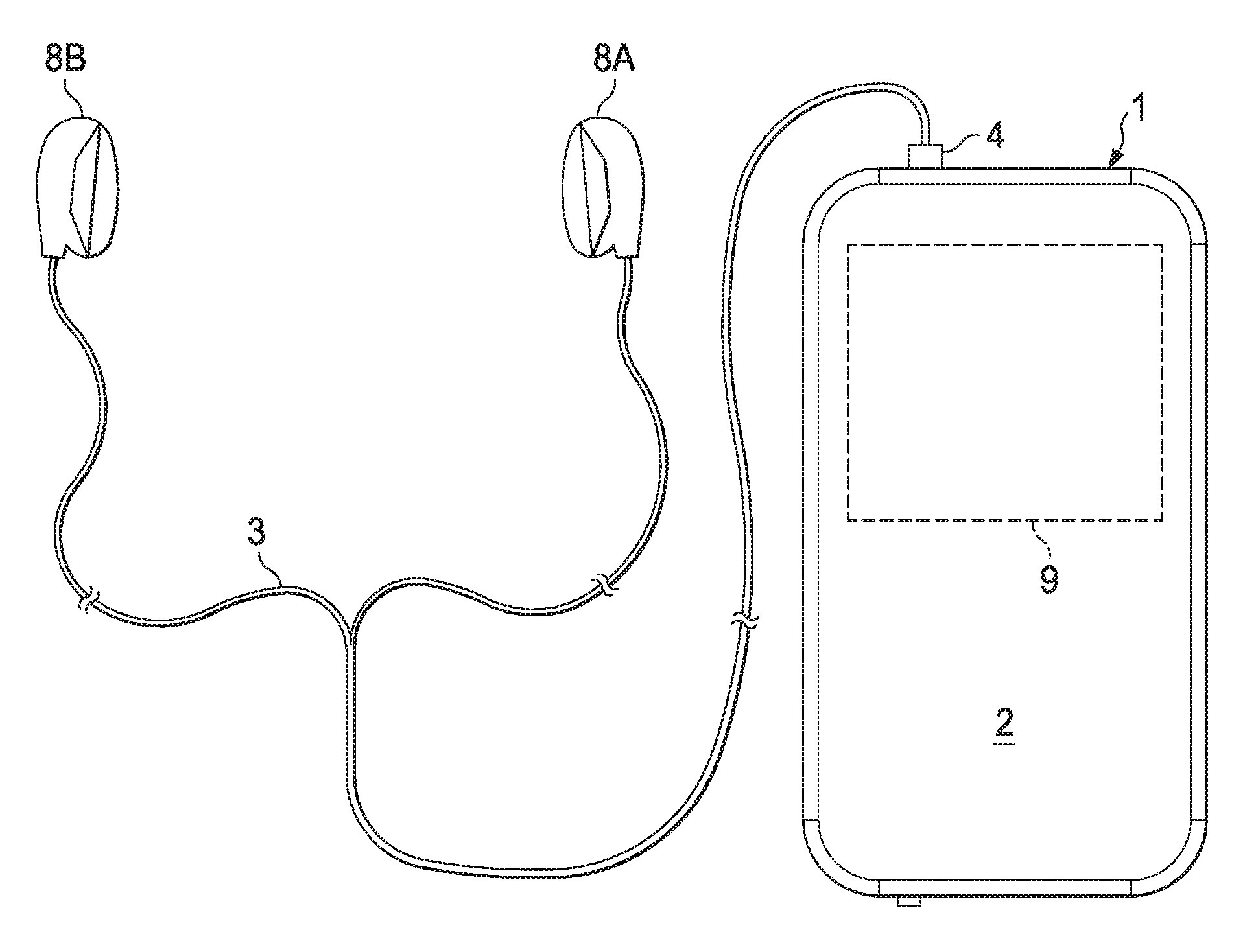
FIG. 1 is an illustration of an example personal audio device 1, in accordance with embodiments of the present disclosure. FIG. 1 depicts personal audio device 1 coupled to a headset 3 in the form of a pair of earbud speakers 8A and 8B. Headset 3 depicted in FIG. 1 is merely an example, and it is understood that personal audio device 1 may be used in connection with a variety of audio transducers, including without limitation, headphones, earbuds, in-ear earphones, and external speakers. A plug 4 may provide for connection of headset 3 to an electrical terminal of personal audio device 1. Personal audio device 1 may provide a display to a user and receive user input using a touch screen 2, or alternatively, a standard liquid crystal display (LCD) may be combined with various buttons, sliders, and/or dials disposed on the face and/or sides of personal audio device 1. As also shown in FIG. 1, personal audio device 1 may include an audio integrated circuit (IC) 9 for generating an analog audio signal for transmission to headset 3 and/or another audio transducer.
FIG. 2 is a block diagram of selected components of an example audio IC 9 of a personal audio device, in accordance with embodiments of the present disclosure. In some embodiments, example audio IC 9 may be used to implement audio IC 9 of FIG. 1. As shown in FIG. 2, a microcontroller core 18 may supply a digital audio input signal DIG_IN to a digital-to-analog converter (DAC) 14, which may convert the digital audio input signal to an analog input signal V.sub.IN. DAC 14 may supply analog signal V.sub.IN to an amplifier 16 which may amplify or attenuate analog input signal V.sub.IN to provide an audio output signal V.sub.OUT, which may operate a speaker, headphone transducer, a line level signal output, and/or other suitable output. In some embodiments, digital audio input signal DIG_IN may be a digital signal with significant out-of-band noise, such as a pulse-density modulated signal, a pulse-width modulated signal, or a pulse-code modulated signal.
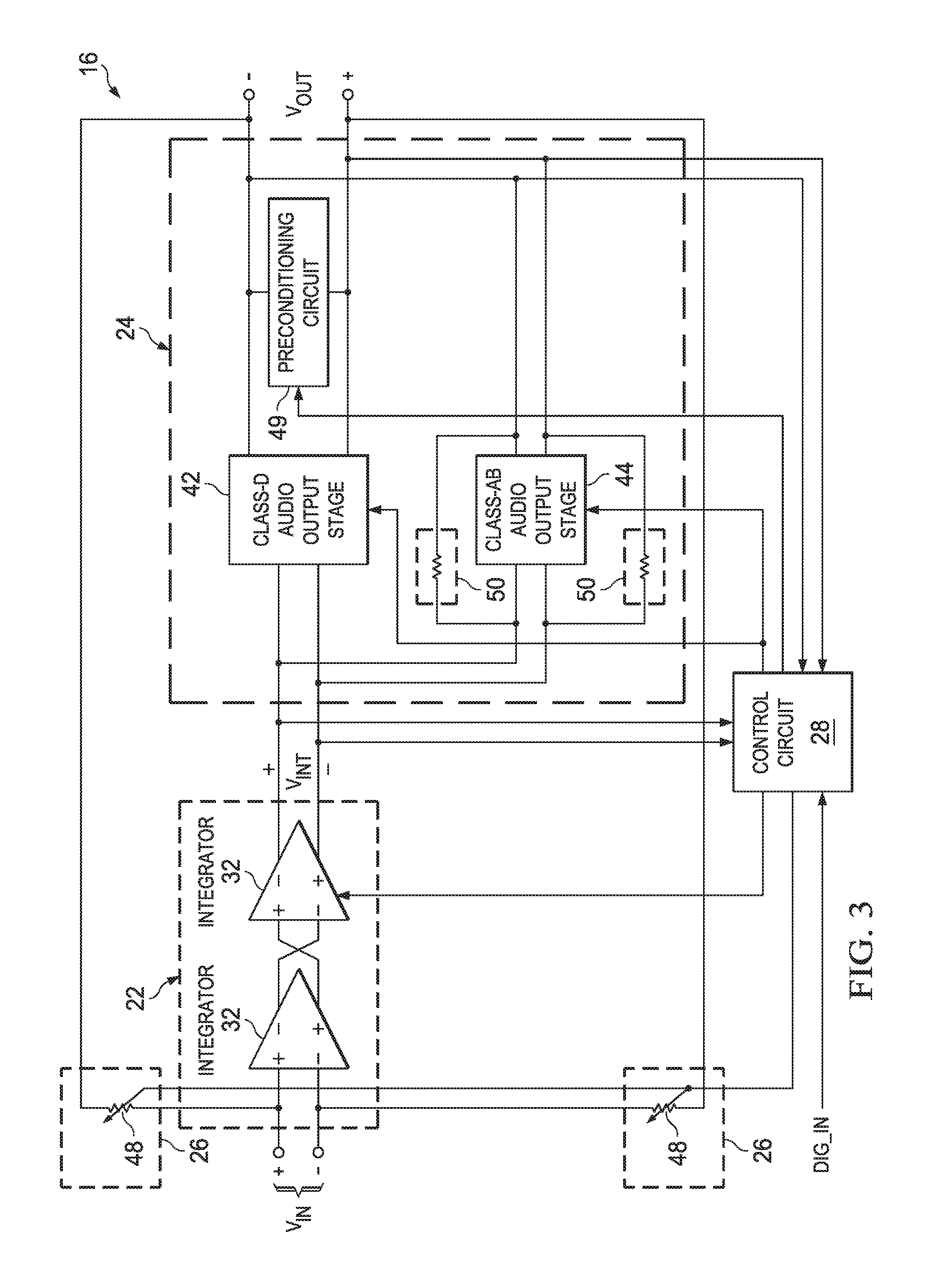
FIG. 3 is a block diagram of selected components of an example amplifier 16, in accordance with embodiments of the present disclosure. As shown in FIG. 3, amplifier 16 may include a first stage 22 (e.g., an analog front end) configured to receive analog input signal V.sub.IN at an amplifier input of amplifier 16 and generate an intermediate signal V.sub.INT which is a function of analog input signal V.sub.IN, a final output stage 24 configured to generate audio output signal V.sub.OUT at an amplifier output of amplifier 16 as a function of intermediate signal V.sub.INT, a signal feedback network 26 coupled between the amplifier output and the amplifier input, and a control circuit 28 for controlling the operation of certain components of amplifier 16, as described in greater detail below.
First stage 22 may include any suitable analog front end circuit for conditioning analog input signal V.sub.IN for use by final output stage 24. For example, first stage 22 may include one or more analog integrators 32 cascaded in series, as shown in FIG. 3.
Final output stage 24 may include any suitable driving circuit for driving audio output signal V.sub.OUT as a function of intermediate signal V.sub.INT (thus, also making audio output signal V.sub.OUT a function of analog input signal V.sub.IN) wherein final output stage 24 is switchable among a plurality of modes including at least a first mode in which final output stage 24 generates audio output signal V.sub.OUT as a modulated output signal which is a function of intermediate signal V.sub.INT and a second mode in which final output stage 24 generates audio output signal V.sub.OUT as an unmodulated output signal which is a function of intermediate signal V.sub.INT. To carry out this functionality, final output stage 24 may include a class-D audio output stage 42 which may be enabled in the first mode (and disabled in the second mode) to generate audio output signal V.sub.OUT as a modulated output signal which is a function of intermediate signal V.sub.INT and a class-AB audio output stage 44 which may be enabled in the second mode (and disabled in the first mode) to generate audio output signal V.sub.OUT as an unmodulated output signal which is a function of intermediate signal V.sub.INT.
Class-D audio output stage 42 may comprise any suitable system, device, or apparatus configured to amplify intermediate signal V.sub.INT and convert intermediate signal V.sub.INT into a series of pulses by pulse-width modulation, pulse-density modulation, or another method of modulation, such that intermediate signal V.sub.INT is converted into a modulated signal in which a characteristic of the pulses of the modulated signal (e.g., pulse widths, pulse density, etc.) is a function of the magnitude of intermediate signal V.sub.INT. After amplification by class-D audio output stage 42, its output pulse train may be converted back to an unmodulated analog signal by passing through a passive low-pass filter, wherein such low-pass filter may be inherent in output circuitry of class-D audio output stage 42 or a load driven by final output stage 24. As shown in FIG. 3, class-D audio output stage 42 may include a control input for receiving a control input from control circuit 28 in order to selectively enable class-D audio output stage 42 during the first mode and disable class-D audio output stage 42 during the second mode (e.g., prevent class-D audio output stage 42 from driving the amplifier output of amplifier 16 by disabling or decoupling a supply voltage from class-D audio output stage 42 or by disabling or decoupling driving devices of the amplifier output of amplifier 16).
Class-AB audio output stage 44 may comprise any suitable system, device, or apparatus configured to amplify intermediate signal V.sub.INT with a linear gain and convert intermediate signal V.sub.INT into an unmodulated audio output signal V.sub.OUT. For example, in some embodiments, unmodulated audio output signal V.sub.OUT may include a continuous-time baseband signal (e.g., an audio baseband signal). As shown in FIG. 3, class-AB audio output stage 44 may include a control input for receiving a control input from control circuit 28 in order to selectively enable class-AB audio output stage 44 during the second mode and disable class-AB audio output stage 44 during the first mode (e.g., prevent class-AB audio output stage 44 from driving the amplifier output of amplifier 16 by disabling or decoupling a supply voltage from class-AB audio output stage 44 or by disabling or decoupling driving devices of the amplifier output of amplifier 16). Example implementations of class-AB audio output stage 44 are depicted in FIGS. 4 and 5 and described in greater detail below.
As shown in FIG. 3, final output stage 24 may include a signal feedback network 50 for feeding back a signal indicative of audio output signal V.sub.OUT to the input of final output stage 24, thus forming a feedback loop around Class-AB audio output stage 44. For example, as shown in FIG. 3, signal feedback network 50 may include resistors and/or other suitable circuit elements.
In some embodiments, a signal gain (e.g., V.sub.OUT/V.sub.INT) of final output stage 24 in the first mode may be approximately equal to the signal gain of final output stage 24 in the second mode. In these and other embodiments, an offset (e.g., direct current offset) of final output stage 24 in the first mode may be approximately equal to the offset of final output stage 24 in the second mode.
As shown in FIG. 3, final output stage 24 may also include a preconditioning circuit 49 coupled to one or both of the output terminals of the amplifier output of amplifier 16, with preconditioning circuit 49 having a control input received from control circuit 28 for controlling functionality of preconditioning circuit 49, as described in greater detail below. In some embodiments, preconditioning circuit 49 may be configured to precondition at least one of a voltage (e.g., voltage V.sub.OUT) and a current of the output (e.g., a current flowing into a load coupled across the terminals of voltage V.sub.OUT) of final output stage 24 prior to switching between modes of final output stage 24 in order to limit audio artifacts caused by switching final output stage 24 between modes. For example, preconditioning circuit 49 may precondition at least one of the voltage and the current of the output of final output stage 24 prior to switching between modes of final output stage 24 by charging each of the output terminals of the output of final output stage 24 to a common mode voltage of a class-AB output driver stage integral to class-AB audio output stage 44. In these and other embodiments, preconditioning circuit 49 may be configured to perform a switching sequence to switch between modes of final output stage 24, such that at all points of the switching sequence, output terminals of the output of final output stage 24 have a known impedance.
Signal feedback network 26 may include any suitable feedback network for feeding back a signal indicative of audio output signal V.sub.OUT to the amplifier input of amplifier 16. For example, as shown in FIG. 3, signal feedback network 26 may include variable feedback resistors 48, wherein resistances of variable feedback resistors 48 are controlled by control signals received from control circuit 28, as described in greater detail below.
Thus, final output stage 24 may operate as an open-loop switched-mode driver in the first mode and may operate as a continuous-time closed-loop amplifier in the second mode. In addition, when the final output stage is operating in the second mode, amplifier 16 may comprise a first feedback loop including signal feedback network 26 and a second feedback loop coupled between the amplifier output and the intermediate output implemented by signal feedback network 50.
Control circuit 28 may include any suitable system, device, or apparatus configured to receive information indicative of digital audio input signal DIG_IN, audio output voltage V.sub.OUT, intermediate signal V.sub.INT, and/or another operational characteristic of amplifier 16, and based at least thereon, control operation of one or more components of amplifier 16. For example, control circuit 28 may be configured to, based on a characteristic of digital audio input signal DIG_IN and/or analog input signal V.sub.IN (e.g., which may be determined from receiving and analyzing digital audio input signal DIG_IN, analog input signal V.sub.IN, intermediate signal V.sub.INT and/or audio output signal V.sub.OUT), switch between the first mode and the second mode of final output stage 24. Such characteristic may include one or more of a frequency of analog input signal V.sub.IN, an amplitude of analog input signal V.sub.IN, a signal-to-noise ratio of analog input signal V.sub.IN, a noise floor of analog input signal V.sub.IN, or another noise characteristic of analog input signal V.sub.IN. For example, in some embodiments, control circuit 28 may be configured to switch final output stage 24 from the first mode to the second mode when an amplitude of analog input signal V.sub.IN decreases below a threshold amplitude, and may be configured to switch final output stage 24 from the second mode to the first mode when an amplitude of analog input signal V.sub.IN increases above the same threshold amplitude or another threshold amplitude. In some embodiments, to reduce audio artifacts associated with switching between modes, control circuit 28 may also be configured to switch between modes only when the amplitude of audio output signal V.sub.OUT is approximately zero (e.g., when a modulated signal generated by class-D audio output stage 42 is at its minimum voltage in its generated pulse train).
In these and other embodiments, control circuit 28 may further be configured to, in order to reduce audio artifacts induced by switching between the two modes, cause final output stage 24 to switch between the first mode and the second mode at an approximate completion of a modulation period of the modulated output signal output by Class-D audio output stage 42, and cause final output stage 24 to switch between the second mode and the first mode at an approximate beginning of another modulation period of the modulated output signal output by Class-D audio output stage 42.
In these and other embodiments, control circuit 28 may further be configured to, in order to reduce audio artifacts induced by switching between the two modes, control preconditioning circuit 49 and components thereof as described elsewhere in this disclosure.
In addition, control circuit 28 may also be configured to perform calibration of final output stage 24. For example, control circuit 28 may receive and analyze intermediate signal V.sub.INT and audio output signal V.sub.OUT to determine a gain of class-D audio output stage 42 (e.g., the signal gain of final output stage 24 in the first mode) and a gain of class-AB audio output stage 44 (e.g., the signal gain of final output stage 24 in the second mode), and based thereon, modify the gain of class-D audio output stage 42 and/or the gain of class-AB audio output stage 44 in order to calibrate the signal gain of final output stage 24 in the second mode to match the signal gain of final output stage 24 in the first mode. As another example, control circuit 28 may receive and analyze intermediate signal V.sub.INT and/or audio output signal V.sub.OUT to determine an offset (e.g., direct current offset) of class-D audio output stage 42 (e.g., the offset of final output stage 24 in the first mode) and an offset of class-AB audio output stage 44 (e.g., the offset of final output stage 24 in the second mode), and based thereon, modify the offset of class-D audio output stage 42 and/or the offset of class-AB audio output stage 44 in order to calibrate the offset of final output stage 24 in the second mode to match the offset of final output stage 24 in the first mode.
In these and other embodiments, control circuit 28 may also be configured to control characteristics of first stage 22 (e.g., integrator 32) and/or signal feedback network 26. Control circuit 28 may maintain such characteristics and structure of first stage 22 and signal feedback network 26 as static when switching between the first mode and the second mode of final output stage 24 and when switching between the second mode and the first mode. Maintaining the characteristics and structure of first stage 22 and signal feedback network 26 as static when switching between modes allows the modes to share the same analog front end and feedback network, thus reducing or minimizing the likelihood of mismatched signal gain and offset between the modes, and thus reducing or minimizing audio artifacts caused by switching between modes. However, after control circuit 28 has switched final output stage 24 to the second mode (e.g., amplifier output driven by class-AB audio output stage 44), control circuit 28 may modify characteristics of first stage 22 and/or signal feedback network 26 in order to decrease a noise floor of amplifier 16. For example, in some embodiments, control circuit 28 may modify characteristics of integrator 32 (e.g., resistances and/or capacitances of filters internal to integrator 32) and/or other components of first stage 22 in order to decrease a noise floor of amplifier 16 when final output stage 24 operates in the second mode. As another example, in these and other embodiments, control circuit 28 may modify characteristics of signal feedback network 26 (e.g., resistances of variable feedback resistors 48) in order to decrease a noise floor of amplifier 16 when final output stage 24 operates in the second mode. When making such modification, control circuit 28 may, before switching final output stage 24 from the second mode to the first mode, return such characteristics to their unmodified states.
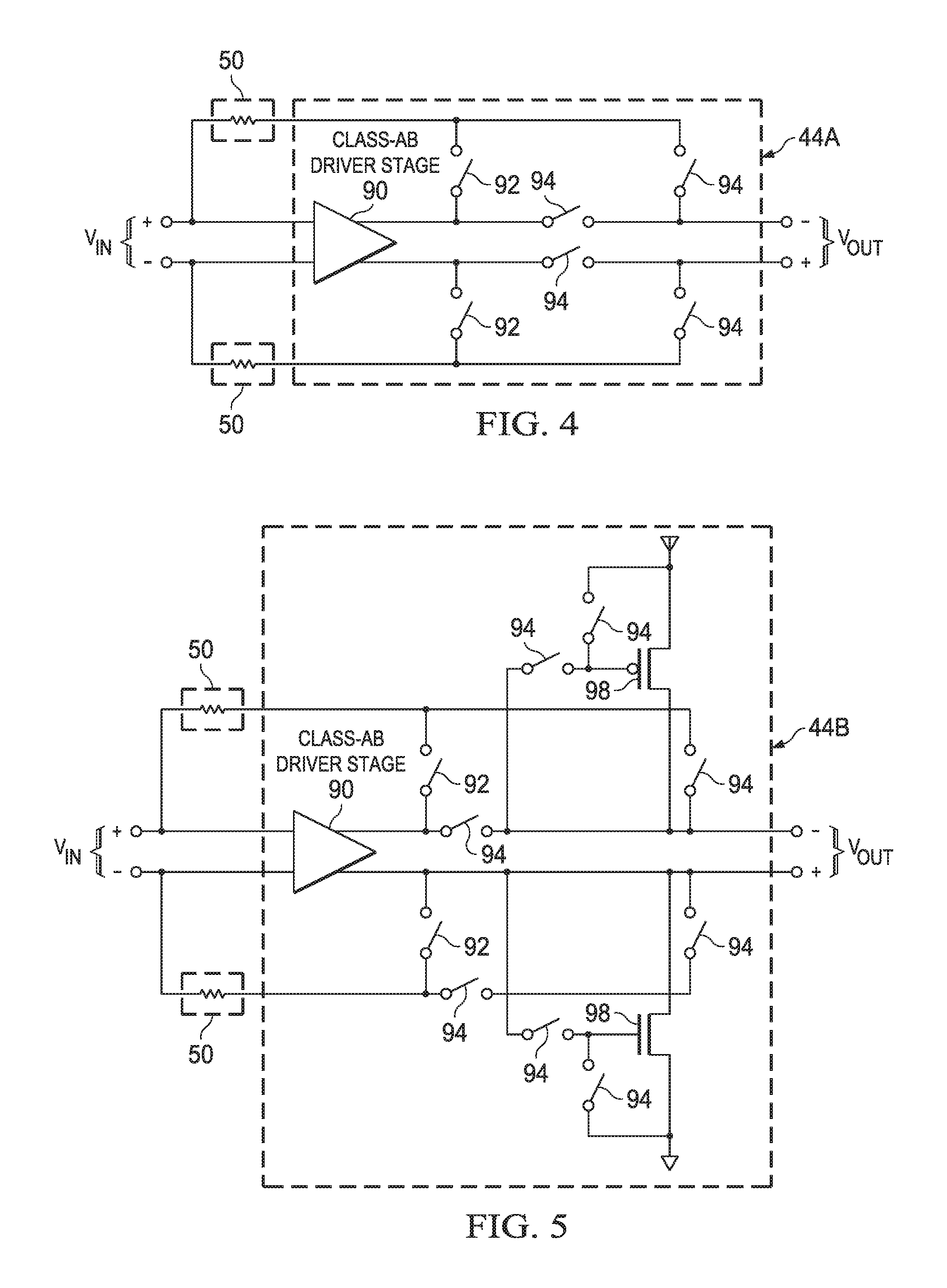
FIG. 4 is a block diagram of selected components of an example class-AB audio output stage 44A, in accordance with embodiments of the present disclosure. In some embodiments, class-AB audio output stage 44 of amplifier 16 may be implemented using class-AB audio output stage 44A. As depicted, class-AB audio output stage 44A may include a class-AB driver stage 90, switches 92, and switches 94 arranged along with signal feedback network 50 as shown in FIG. 4. In operation, when switching between modes of final output stage 24 from its class-D mode of operation to class-AB mode of operation, such switching may first involve powering on components of class-AB audio output stage 44A including class-AB driver stage 90 from a powered-off or powered-down state. After powering on components of class-AB audio output stage 44A including class-AB driver stage 90, switches 92 may be activated (e.g., closed, enabled, turned on) and switches 94 deactivated (e.g., opened, disabled, turned off) under the control of control signals communicated from control circuit 28 to allow operation of class-AB audio output stage 44A to settle into a normal steady-state operation before coupling the output of class-AB driver stage 90 to the output of final output stage 24. After class-AB output stage 44A has settled (and other conditions for switching between modes of final output stage 24 have been satisfied, as described elsewhere in this disclosure), switches 94 may be activated and switches 92 deactivated under the control of control signals communicated from control circuit 28 in order to couple the output of class-AB driver stage 90 to the output of final output stage 24.
FIG. 5 is a block diagram of selected components of another example class-AB audio output stage 44B, in accordance with embodiments of the present disclosure. In some embodiments, class-AB audio output stage 44 of amplifier 16 may be implemented using class-AB audio output stage 44B. Class-AB audio output stage 44B may in many respects be similar to class-AB audio output stage 44A of FIG. 4, and thus, only the main differences between class-AB audio output stage 44B and class-AB audio output stage 44A may be described below. As shown in FIG. 5, class-AB audio output stage 44B may include a p-type metal-oxide-semiconductor field-effect transistor (p-MOSFET) 96, an n-type metal-oxide-semiconductor field-effect transistor (N-MOSFET) 98, and additional switches 94 beyond those present in class-AB audio output stage 44A of FIG. 4. The characteristics of p-MOSFET 96 and N-MOSFET 98 may be such that they replicate characteristics of analogous devices integral to that of class-AB driver stage 90.
Thus, in operation, when switching between modes of final output stage 24 from its class-D mode of operation to class-AB mode of operation, switches 92 may be activated and switches 94 deactivated under the control of control signals communicated from control circuit 28 to allow operation of class-AB audio output stage 44B to settle into a normal steady-state operation before coupling the output of class-AB driver stage 90 to the output of final output stage 24. After class-AB output stage 44B has settled (and other conditions for switching between modes of final output stage 24 have been satisfied, as described elsewhere in this disclosure), switches 94 may be activated and switches 92 deactivated under the control of control signals communicated from control circuit 28 in order to couple the output of class-AB driver stage 90 to the output of final output stage 24. Accordingly, during the process of switching between modes of final output stage 24 from its class-D mode of operation to class-AB mode of operation, the replica of class-AB driver stage 90 formed by p-MOSFET 96 and N-MOSFET 98 may precondition at least one of the voltage (e.g., voltage V.sub.OUT) and the current of the output of final output stage 28 by charging the output to a common mode voltage of class-AB driver stage 90 using a replica of class-AB driver stage 90 to provide the common mode voltage.
Although FIG. 5 depicts that the replica of class-AB driver stage 90 formed by p-MOSFET 96 and N-MOSFET 98 is present within class-AB audio output stage 44B, in some embodiments, such replica and one or more other components depicted in FIG. 5 as integral to class-AB audio output stage 44B may instead be integral to preconditioning circuit 49 described elsewhere herein.
FIG. 6 is a block diagram of selected components of an example preconditioning circuit 49A, in accordance with embodiments of the present disclosure. In some embodiments, preconditioning circuit 49 of amplifier 16 may be implemented using preconditioning circuit 49A. As shown in FIG. 6, preconditioning circuit 49A may include a clamp 46 and a quick charge circuit 47. Clamp 46, which may be embodied as a switch, may be coupled between the output terminals of the amplifier output of amplifier 16, with clamp 46 having a control input received from control circuit 28 for selectively enabling clamp 46 (to short the output terminals together) and disabling clamp 46, as described in greater detail below. Quick charge circuit 47 may include any suitable circuit for preconditioning at least one of the voltage (e.g., voltage V.sub.OUT) and the current of the output of final output stage 24 to a particular voltage and/or current (e.g., to a common-mode voltage of class-AB audio output stage 44).
FIG. 7 is a circuit diagram of selected components of an example quick charge circuit 47, in accordance with embodiments of the present disclosure. As depicted in FIG. 7, quick charge circuit 47 may include a flip-flop 100, logic NOR gate 102, n-MOSFET 104, n-MOSFET 106, p-MOSFET 108, n-MOSFET 110, p-MOSFET 112, and n-MOSFET 114 arranged as shown in FIG. 7. In operation, when quick charge circuit 47 is enabled in accordance with one or more control signals communicated from control circuit 28, quick charge circuit 47 may charge the output terminals (which may be coupled together via clamp 46) of final output stage 24 to a common mode voltage V.sub.cm, which may be a common mode voltage of class-AB audio output stage 44. In operation, n-MOSFET 104 and n-MOSFET 106 may charge the output terminals of final output stage 24, with a current-mode feedback which controls the voltage to which the output terminals are charged. Accordingly, quick charge circuit 47 may also precondition a current on the output of final output stage 24 based on a load present across the terminals of the output of final output stage 24.
FIG. 8 is a block diagram of selected components of another example preconditioning circuit 49B, in accordance with embodiments of the present disclosure. In some embodiments, preconditioning circuit 49 of amplifier 16 may be implemented using preconditioning circuit 49B. As shown in FIG. 8, preconditioning circuit 49B may include a clamp 46, a capacitor 39, and switches 41 and 43 arranged as shown.
Clamp 46 of preconditioning circuit 49B may be similar to that of clamp 46 of preconditioning circuit 49A. When preconditioning circuit 49B is enabled under the control of control signals communicated from control circuit 28, clamp 46 may be enabled to short the output terminals of final output stage 24 together, switch 43 may be activated, and switch 41 deactivated to allow charge present on capacitor 39 to charge each of the output terminals of final output stage 24 to a common mode voltage V.sub.cm. When preconditioning circuit 49B is disabled under the control of control signals communicated from control circuit 28, clamp 46 may be disabled, switch 41 may be activated, and switch 43 deactivated to allow capacitor 39 to charge to common mode voltage V.sub.cm. Those of skill in the art may recognize that a dual equivalent current source and inductor may be substituted in place of voltage V.sub.cm and capacitor 39 such that the inductor may precondition a current of the output terminals of final output stage 24 when preconditioning circuit 49B is enabled.
FIG. 9 is a flow chart of an example method 51 for switching between a first mode of a final output stage 24 of amplifier 16 and a second mode of final output stage 24 of amplifier 16, in accordance with embodiments of the present disclosure. According to some embodiments, method 51 begins at step 52. As noted above, teachings of the present disclosure are implemented in a variety of configurations of personal audio device 1. As such, the preferred initialization point for method 51 and the order of the steps comprising method 51 may depend on the implementation chosen.
At step 52, control circuit 28 may monitor intermediate signal V.sub.INT, audio output signal V.sub.OUT, or another signal indicative of analog input signal V.sub.IN, to determine if analog input signal V.sub.IN has decreased from above to below a threshold amplitude. If analog input signal V.sub.IN has decreased from above to below the threshold amplitude, method 51 may proceed to step 53. Otherwise, method 51 may remain at step 52 until such threshold amplitude crossing occurs.
At step 53, control circuit 28 may monitor audio output signal V.sub.OUT to determine when the amplitude of audio output signal V.sub.OUT is approximately zero (e.g., when a modulated signal generated by class-D audio output stage 42 is at its minimum voltage in its generated pulse train). If audio output signal V.sub.OUT has reached approximately zero, method 51 may proceed to step 54. Otherwise, method 51 may remain at step 53 until audio output signal V.sub.OUT reaches approximately zero.
At step 54, control circuit 28 may cause class-AB amplifier 44 to power on from a powered-off or powered-down state, which state class-AB amplifier 44 may operate in order to save power when final output stage 24 is operating in the class-D mode.
At step 55, control circuit 28 may monitor audio output signal V.sub.OUT to determine when class-AB amplifier 44 has settled into a steady-state operation from being powered on. Once class-AB amplifier 44 has settled, method 51 may proceed to step 56.
At step 56, control circuit 28 may enable clamp 46, thus shorting the output terminals at the amplifier output of amplifier 16 together, forcing audio output signal V.sub.OUT to zero. At step 57, control circuit 28 may disable class-D amplifier 42. For example, class-D amplifier 42 may be disabled by deactivating switches integral to class-D amplifier 42 such that the output terminals of class-D amplifier 42 are in a high-impedance state.
At step 58, class-AB audio output stage 44 and/or preconditioning circuit 49 may ramp a common mode voltage of audio output signal V.sub.OUT to a predetermined value (e.g., a common-mode voltage equal to one-half of a supply voltage for class-AB audio output stage 44). At step 60, control circuit 28 may fully enable class-AB audio output stage 44 such that audio output signal V.sub.OUT is an unmodulated signal which is a function of intermediate signal V.sub.INT. For example, class-AB amplifier 44 may be enabled by activating switches integral to class-AB amplifier 44 (e.g., switches 94 depicted in FIGS. 4 and 5) such that the output terminals of a class-AB driver stage (e.g., class-AB driver stage 90) integral to class-AB amplifier 44 are coupled to the output terminals of final output stage 24. In some embodiments, steps 56 through 60 may take place when the modulated output signal output by class-D audio output stage 42 is at an approximate completion of a modulation period.
At step 62, control circuit 28 may disable clamp 46, thus allowing audio output signal V.sub.OUT to take on a non-zero value driven by class-AB audio output stage 44. After completion of step 62, method 51 may end.
Although FIG. 9 discloses a particular number of steps to be taken with respect to method 51, method 51 may be executed with greater or fewer steps than those depicted in FIG. 9. In addition, although FIG. 9 discloses a certain order of steps to be taken with respect to method 51, the steps comprising method 51 may be completed in any suitable order.
Method 51 may be implemented using personal audio device 1 or any other system operable to implement method 51. In certain embodiments, method 51 may be implemented partially or fully in software and/or firmware embodied in computer-readable media and executable by a controller.
FIG. 10 is a flow chart of an example method 70 for switching between a second mode of final output stage 24 of amplifier 16 and a first mode of final output stage 24 of amplifier 16, in accordance with embodiments of the present disclosure. According to some embodiments, method 70 begins at step 72. As noted above, teachings of the present disclosure are implemented in a variety of configurations of personal audio device 1. As such, the preferred initialization point for method 70 and the order of the steps comprising method 70 may depend on the implementation chosen.
At step 72, control circuit 28 may monitor intermediate signal V.sub.INT, audio output signal V.sub.OUT, or another signal indicative of analog input signal V.sub.IN, to determine if analog input signal V.sub.IN has increased from below to above a threshold amplitude (which may be the same threshold as that of step 52, or a different threshold). If analog input signal V.sub.IN has increased from below to above the threshold amplitude, method 70 may proceed to step 73. Otherwise, method 70 may remain at step 72 until such threshold amplitude crossing occurs.
At step 73, control circuit 28 may monitor audio output signal V.sub.OUT to determine when the amplitude of audio output signal V.sub.OUT is approximately zero (e.g., when audio output signal V.sub.OUT experiences a zero crossing). If audio output signal V.sub.OUT is approximately zero, method 70 may proceed to step 74. Otherwise, method 70 may remain at step 73 until audio output signal V.sub.OUT is approximately zero.
At step 74, control circuit 28 may cause class-D amplifier 42 to power on from a powered-off or powered-down state, which state class-D amplifier 42 may operate in order to save power when final output stage 24 is operating in the class-AB mode.
At step 75, control circuit 28 may monitor audio output signal V.sub.OUT to determine when class-D amplifier 42 has settled into a steady-state operation from being powered on. Once class-D amplifier 42 has settled, method 70 may proceed to step 76.
At step 76, control circuit 28 may enable clamp 46, thus shorting the output terminals at the amplifier output of amplifier 16 together, forcing audio output signal V.sub.OUT to zero. At step 77, control circuit 28 may disable class-AB amplifier 44. For example, class-AB amplifier 44 may be disabled by activating switches integral to class-AB amplifier 44 (e.g., switches 94 depicted in FIGS. 4 and 5) such that the output terminals of a class-AB driver stage (e.g., class-AB driver stage 90) integral to class-AB amplifier 44 are decoupled to the output terminals of final output stage 24.
At step 78, preconditioning circuit 49 (or another auxiliary amplifier, not shown in FIG. 3) may ramp a common mode voltage of audio output signal V.sub.OUT to zero. At step 80, control circuit 28 may fully enable class-D audio output stage 42 such that audio output signal V.sub.OUT is a modulated signal which is a function of intermediate signal V.sub.INT. For example, class-D amplifier 42 may be enabled by activating switches integral to class-D amplifier 42 such that the output terminals of class-D amplifier 42 are coupled to the output terminals of final output stage 24. In some embodiments, steps 76 through 80 may take place when the modulated output signal output by class-D audio output stage 42 is at an approximate beginning of a modulation period.
At step 82, control circuit 28 may disable clamp 46, thus allowing audio output signal V.sub.OUT to take on a non-zero value driven by class-D audio output stage 42. After completion of step 82, method 70 may end.
Although FIG. 10 discloses a particular number of steps to be taken with respect to method 70, method 70 may be executed with greater or fewer steps than those depicted in FIG. 10. In addition, although FIG. 10 discloses a certain order of steps to be taken with respect to method 70, the steps comprising method 70 may be completed in any suitable order.
Method 70 may be implemented using personal audio device 1 or any other system operable to implement method 70. In certain embodiments, method 70 may be implemented partially or fully in software and/or firmware embodied in computer-readable media and executable by a controller.
A particular challenge in determining whether to switch between modes of final output stage 24 is that detection of in-band signal levels for such switching requires low-pass filtering. However, such a low-pass filter adds latency to the determination of whether to switch nodes. Thus, for a rising magnitude of an input signal, the latency in such determination of whether to switch modes (e.g., from the second mode with Class AB output stage 44 enabled to the first mode with Class D output stage 42 enabled) may cause switching to occur too slowly, such that signal clipping of the output signal occurs.
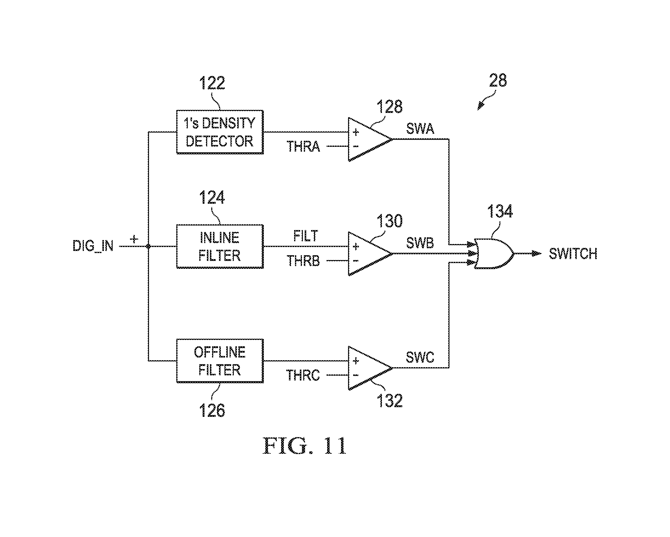
FIG. 11 is a block diagram of selected components of an example control circuit 28 of amplifier 16 depicted in FIG. 3, in accordance with embodiments of the present disclosure. Such components of control circuit 28 may reduce or eliminate the challenge described above with respect to low-pass filter inducing latency in the control of switching between modes.
As shown in FIG. 11, control circuit 28 may include a ones density detector 122, an inline filter 124, an offline filter 126, comparators 128, 130, and 132, and a logical OR gate 134.
Ones density detector 122 may include any system, device, or apparatus configured to determine (particularly in embodiments in which digital audio input signal DIG_IN is a pulse-density modulated signal) a density of logical ones of digital audio input signal DIG_IN and generate an output signal indicative of such density. Such output signal may be received by comparator 128 and compared by comparator 128 against a threshold density THRA in order to generate an intermediate switching signal SWA.
Inline filter 124 may include any suitable filter configured to receive digital audio input signal DIG_IN and low-pass filter digital audio input signal DIG_IN to generate a low-pass filtered version of digital audio input signal DIG_IN. Such filtered signal may be received by comparator 130 and compared by comparator 130 against a threshold density THRB in order to generate an intermediate switching signal SWB. As its name indicates, inline filter 124 may be integral to the signal path between digital audio input signal DIG_IN and audio output signal V.sub.OUT, and thus may generate an output signal FILT that may represent an intermediate voltage internal to DAC 14, first stage 22, or any other suitable portion of amplifier 16 comprising the signal path between digital audio input signal DIG_IN and audio output signal V.sub.OUT.
Offline filter 126 may include any suitable filter configured to receive digital audio input signal DIG_IN and low-pass filter digital audio input signal DIG_IN to generate a low-pass filtered version of digital audio input signal DIG_IN. Such filtered signal may be received by comparator 132 and compared by comparator 132 against a threshold density THRC in order to generate an intermediate switching signal SWC. As its name indicates, offline filter 126 may be external to the signal path between digital audio input signal DIG_IN and audio output signal V.sub.OUT. Because it is external to the signal path, offline filter 126 may be of a higher latency (and thus greater accuracy) than inline filter 124.
Logical OR gate 134 may perform a logical OR operation on the intermediate switching signals SWA, SWB, and SWC and generate a switching signal SWITCH that indicates that final output stage 24 of amplifier 16 should switch from the second mode (e.g., Class-AB output stage 44 enabled) to the first mode (e.g., Class-D output stage 42 enabled) in response to digital audio input signal DIG_IN increasing in magnitude. Accordingly, an assertion of any of switching signals SWA, SWB, and SWC may trigger a switch between the second mode to the first mode of final output stage 24. Due to their individual characteristics, the combination of ones density detector 122 and comparator 128 may be best suited for detecting threshold crossings of fast-rising signal magnitudes of digital audio input signal DIG_IN, the combination of inline filter 124 and comparator 130 may be best suited for detecting threshold crossings of medium-rising signal magnitudes of digital audio input signal DIG_IN, and the combination of offline filter 126 and comparator 132 may be best suited for detecting threshold crossings of slow-rising signal magnitudes of digital audio input signal DIG_IN. Accordingly, control circuit 28 may efficiently switch from the second mode (e.g., Class-AB output stage 44 enabled) to the first mode (e.g., Class-D output stage 42 enabled) of final output stage 24 while reducing or eliminating audio artifacts of switching.
The various thresholds THRA, THRB, and THRC may be equal/equivalent, or may be different. For example, in some embodiments, threshold THRB may be larger than threshold THRC to account for noise present in inline filter 124 and/or noise present in all or a portion of the signal path between digital audio input signal DIG_IN and audio output signal V.sub.OUT. Thus, control circuit 28 may set threshold THRB relative to threshold THRC by measuring a difference between the filtered signal output by inline filter 124 and the filtered signal output by offline filter 126 when digital audio input signal DIG_IN is zero, such that the difference is indicative of noise present in inline filter 124, and setting threshold THRB based on the difference.
Although the foregoing contemplates use of the components of control circuit 28 depicted in FIG. 11 to switch between a second mode and a first mode of final output stage 24, the systems and methods used herein may be applied to any audio system which employs a threshold for switching between operating modes of the audio system and/or active signal paths of the audio system. For example, in some embodiments, systems and methods identical or similar to those described above may be employed for use in noise gating, whereby for low magnitudes of an audio input signal, an output signal of an audio system is forced to zero, so as to avoid audio output of noise present in the signal path. Thus, referring to FIG. 11, control circuit 28 may set threshold THRB for exiting a noise-gating mode of operation of an audio system by measuring a difference between the filtered signal output by inline filter 124 and the filtered signal output by offline filter 126 when digital audio input signal DIG_IN is zero, such that the difference is indicative of noise present in an audio signal path, and setting threshold THRB based on the difference.
As used herein, when two or more elements are referred to as "coupled" to one another, such term indicates that such two or more elements are in electronic communication or mechanical communication, as applicable, whether connected indirectly or directly, with or without intervening elements.
This disclosure encompasses all changes, substitutions, variations, alterations, and modifications to the exemplary embodiments herein that a person having ordinary skill in the art would comprehend. Similarly, where appropriate, the appended claims encompass all changes, substitutions, variations, alterations, and modifications to the exemplary embodiments herein that a person having ordinary skill in the art would comprehend. Moreover, reference in the appended claims to an apparatus or system or a component of an apparatus or system being adapted to, arranged to, capable of, configured to, enabled to, operable to, or operative to perform a particular function encompasses that apparatus, system, or component, whether or not it or that particular function is activated, turned on, or unlocked, as long as that apparatus, system, or component is so adapted, arranged, capable, configured, enabled, operable, or operative.
All examples and conditional language recited herein are intended for pedagogical objects to aid the reader in understanding the invention and the concepts contributed by the inventor to furthering the art, and are construed as being without limitation to such specifically recited examples and conditions. Although embodiments of the present inventions have been described in detail, it should be understood that various changes, substitutions, and alterations could be made hereto without departing from the spirit and scope of the disclosure.
* * * * *
References
D00000
D00001
D00002
D00003
D00004
D00005
D00006
XML
uspto.report is an independent third-party trademark research tool that is not affiliated, endorsed, or sponsored by the United States Patent and Trademark Office (USPTO) or any other governmental organization. The information provided by uspto.report is based on publicly available data at the time of writing and is intended for informational purposes only.
While we strive to provide accurate and up-to-date information, we do not guarantee the accuracy, completeness, reliability, or suitability of the information displayed on this site. The use of this site is at your own risk. Any reliance you place on such information is therefore strictly at your own risk.
All official trademark data, including owner information, should be verified by visiting the official USPTO website at www.uspto.gov. This site is not intended to replace professional legal advice and should not be used as a substitute for consulting with a legal professional who is knowledgeable about trademark law.