Method and apparatus for the monolithic encapsulation of a micro-scale inertial navigation sensor suite
Kirby , et al.
U.S. patent number 10,308,505 [Application Number 14/456,808] was granted by the patent office on 2019-06-04 for method and apparatus for the monolithic encapsulation of a micro-scale inertial navigation sensor suite. This patent grant is currently assigned to HRL Laboratories, LLC. The grantee listed for this patent is HRL LABORATORIES LLC. Invention is credited to David T. Chang, Deborah J. Kirby, Hung Nguyen, Raviv Perahia, Frederic P. Stratton.
| United States Patent | 10,308,505 |
| Kirby , et al. | June 4, 2019 |
Method and apparatus for the monolithic encapsulation of a micro-scale inertial navigation sensor suite
Abstract
A device preferably for use in an inertial navigation system the device having a single IC wafer; a plurality of sensors bonded to bond regions on said single IC wafer, at least one of said bond regions including an opening therein in gaseous communication with a pressure chamber associated with at least one of the plurality of said sensors; and a plurality of caps encapsulating said plurality of sensors, at least one of said plurality of caps forming at least a portion of said pressure chamber. A method of making the device is also disclosed.
| Inventors: | Kirby; Deborah J. (Calabasas, CA), Perahia; Raviv (Calabasas, CA), Nguyen; Hung (Los Angeles, CA), Stratton; Frederic P. (Beverly Hills, CA), Chang; David T. (Calabasas, CA) | ||||||||||
|---|---|---|---|---|---|---|---|---|---|---|---|
| Applicant: |
|
||||||||||
| Assignee: | HRL Laboratories, LLC (Malibu,
CA) |
||||||||||
| Family ID: | 66673466 | ||||||||||
| Appl. No.: | 14/456,808 | ||||||||||
| Filed: | August 11, 2014 |
| Current U.S. Class: | 1/1 |
| Current CPC Class: | B81B 3/00 (20130101); B81C 1/00285 (20130101); G01C 19/5783 (20130101); B81B 3/0021 (20130101); B81B 7/02 (20130101); G01C 21/18 (20130101); B81C 2203/0172 (20130101); B81B 2207/012 (20130101); B81B 2201/0235 (20130101); B81B 2201/0242 (20130101); B81B 2201/0264 (20130101) |
| Current International Class: | B81B 3/00 (20060101); B81C 1/00 (20060101); G01C 21/18 (20060101) |
References Cited [Referenced By]
U.S. Patent Documents
| 392650 | November 1888 | Watrous |
| 2487165 | November 1949 | Miller |
| 3390287 | June 1968 | Sonderegger |
| 3766616 | October 1973 | Staudte |
| 4426769 | January 1984 | Grabbe |
| 4442574 | April 1984 | Wanuga et al. |
| 4618262 | October 1986 | Maydan et al. |
| 4655081 | April 1987 | Burdess |
| 4870313 | September 1989 | Hirama et al. |
| 4898031 | February 1990 | Oikawa et al. |
| 4944836 | July 1990 | Beyer et al. |
| 5203208 | April 1993 | Bernstein |
| 5226321 | July 1993 | Varnham et al. |
| 5260596 | November 1993 | Dunn et al. |
| 5421312 | June 1995 | Dawson |
| 5480747 | January 1996 | Vasudev |
| 5530408 | June 1996 | Vig et al. |
| 5552016 | September 1996 | Ghanayem |
| 5578976 | November 1996 | Yao et al. |
| 5589724 | December 1996 | Satoh et al. |
| 5604312 | February 1997 | Lutz |
| 5605490 | February 1997 | Laffey et al. |
| 5644139 | July 1997 | Allen et al. |
| 5646346 | July 1997 | Okada |
| 5648849 | July 1997 | Canteloup et al. |
| 5658418 | August 1997 | Coronel et al. |
| 5665915 | September 1997 | Kobayashi et al. |
| 5666706 | September 1997 | Tomita et al. |
| 5668057 | September 1997 | Eda et al. |
| 5728936 | March 1998 | Lutz |
| 5783749 | July 1998 | Lee et al. |
| 5894090 | April 1999 | Tang et al. |
| 5905202 | May 1999 | Kubena et al. |
| 5920012 | July 1999 | Pinson |
| 5928532 | July 1999 | Koshimizu et al. |
| 5942445 | August 1999 | Kato et al. |
| 5959206 | September 1999 | Ryrko |
| 5981392 | November 1999 | Oishi |
| 5987985 | November 1999 | Okada |
| 6009751 | January 2000 | Ljung |
| 6044705 | April 2000 | Neukermans et al. |
| 6049702 | April 2000 | Tham et al. |
| 6081334 | June 2000 | Grimbergen et al. |
| 6089088 | July 2000 | Charvet |
| 6094985 | August 2000 | Kapels et al. |
| 6114801 | September 2000 | Tanaka et al. |
| 6145380 | November 2000 | MacGugan et al. |
| 6151964 | November 2000 | Nakajima |
| 6155115 | December 2000 | Ljung |
| 6164134 | December 2000 | Cargille |
| 6182352 | February 2001 | Deschenes et al. |
| 6196059 | March 2001 | Kosslinger |
| 6204737 | March 2001 | Ella |
| 6207008 | March 2001 | Kijima |
| 6236145 | May 2001 | Biernacki |
| 6250157 | June 2001 | Touge |
| 6263552 | July 2001 | Takeuchi et al. |
| 6282958 | September 2001 | Fell et al. |
| 6289733 | September 2001 | Challoner et al. |
| 6297064 | October 2001 | Koshimizu |
| 6349597 | February 2002 | Folkmer et al. |
| 6367326 | April 2002 | Okada |
| 6367786 | April 2002 | Gutierrez et al. |
| 6413682 | July 2002 | Shibano et al. |
| 6417925 | July 2002 | Naya |
| 6424418 | July 2002 | Kawabata et al. |
| 6426296 | July 2002 | Okojie |
| 6432824 | August 2002 | Yanagisawa |
| 6481284 | November 2002 | Geen et al. |
| 6481285 | November 2002 | Shkel et al. |
| 6492195 | December 2002 | Nakanishi |
| 6513380 | February 2003 | Reeds et al. |
| 6514767 | February 2003 | Natan |
| 6515278 | February 2003 | Wine et al. |
| 6571629 | June 2003 | Kipp |
| 6584845 | July 2003 | Gutierrez et al. |
| 6614529 | September 2003 | Tang |
| 6621158 | September 2003 | Martin et al. |
| 6627067 | September 2003 | Branton et al. |
| 6628177 | September 2003 | Clark et al. |
| 6629460 | October 2003 | Challoner |
| 6651027 | November 2003 | McCall et al. |
| 6662656 | December 2003 | Jeanroy |
| 6686807 | February 2004 | Giousouf et al. |
| 6710681 | March 2004 | Figueredo et al. |
| 6715352 | April 2004 | Tracy |
| 6744335 | June 2004 | Ryhanen |
| 6750728 | June 2004 | Takahashi et al. |
| 6756304 | June 2004 | Robert |
| 6768396 | July 2004 | Klee et al. |
| 6796179 | September 2004 | Bae et al. |
| 6806557 | October 2004 | Ding |
| 6815228 | November 2004 | Usui et al. |
| 6856217 | February 2005 | Clark et al. |
| 6862398 | March 2005 | Elkind et al. |
| 6883374 | April 2005 | Fell et al. |
| 6915215 | July 2005 | Closkey et al. |
| 6933164 | August 2005 | Kubena |
| 6943484 | September 2005 | Clark et al. |
| 6985051 | January 2006 | Nguyen et al. |
| 7040163 | May 2006 | Shcheglov |
| 7057331 | June 2006 | Shimodaira et al. |
| 7118657 | October 2006 | Goloychenko et al. |
| 7152290 | December 2006 | Junhua et al. |
| 7168318 | January 2007 | Challoner et al. |
| 7211933 | May 2007 | Kawakubo |
| 7224245 | May 2007 | Song et al. |
| 7232700 | June 2007 | Kubena |
| 7234214 | June 2007 | Xu |
| 7237315 | July 2007 | Kubena |
| 7281425 | October 2007 | Chikovani |
| 7295088 | November 2007 | Nguyen et al. |
| 7317354 | January 2008 | Lee |
| 7404325 | July 2008 | Delevoye |
| 7446628 | November 2008 | Morris, III |
| 7459099 | December 2008 | Kubena et al. |
| 7459992 | December 2008 | Matsuda et al. |
| 7479846 | January 2009 | Inoue et al. |
| 7490390 | February 2009 | Kawakubo et al. |
| 7543496 | June 2009 | Ayazi et al. |
| 7551054 | June 2009 | Mizuno et al. |
| 7555824 | July 2009 | Chang |
| 7557493 | July 2009 | Fujimoto |
| 7559130 | July 2009 | Kubena et al. |
| 7564177 | July 2009 | Yoshimatsu et al. |
| 7579748 | August 2009 | Kuroda |
| 7579926 | August 2009 | Jhung |
| 7581443 | September 2009 | Kubena |
| 7663196 | February 2010 | Liu et al. |
| 7671427 | March 2010 | Kim et al. |
| 7675224 | March 2010 | Tanaya |
| 7750535 | July 2010 | Kubena et al. |
| 7757393 | July 2010 | Ayazi et al. |
| 7791431 | September 2010 | Piazza et al. |
| 7802356 | September 2010 | Chang |
| 7830074 | November 2010 | Kubena |
| 7872548 | January 2011 | Nishihara et al. |
| 7884930 | February 2011 | Kirby |
| 7895892 | March 2011 | Aigner |
| 7994877 | August 2011 | Kubena |
| 8138016 | March 2012 | Chang |
| 8151640 | April 2012 | Kubena |
| 8176607 | May 2012 | Kubena |
| 8305154 | November 2012 | Kubena |
| 8522612 | September 2013 | Kubena |
| 8569937 | October 2013 | Kubena |
| 8765615 | July 2014 | Chang |
| 8766745 | July 2014 | Kubena |
| 9038459 | May 2015 | Kubena |
| 9404748 | August 2016 | Perahia |
| 2002/0066317 | June 2002 | Lin |
| 2002/0072246 | June 2002 | Goo et al. |
| 2002/0074947 | June 2002 | Tsukamoto |
| 2003/0003608 | January 2003 | Arikado et al. |
| 2003/0010123 | January 2003 | Malvern et al. |
| 2003/0029238 | February 2003 | Challoner |
| 2003/0196490 | October 2003 | Cardarelli |
| 2003/0205948 | November 2003 | Lin et al. |
| 2004/0055380 | March 2004 | Shcheglov et al. |
| 2004/0065864 | April 2004 | Vogt et al. |
| 2004/0189311 | September 2004 | Glezer |
| 2004/0211052 | October 2004 | Kubena et al. |
| 2004/0219700 | November 2004 | Silverbrook |
| 2004/0239341 | December 2004 | Aoyagi et al. |
| 2005/0034822 | February 2005 | Kim et al. |
| 2005/0062368 | March 2005 | Hirasawa |
| 2005/0093659 | May 2005 | Larson et al. |
| 2005/0156309 | July 2005 | Fujii |
| 2005/0172714 | August 2005 | Challoner |
| 2005/0260792 | November 2005 | Patel |
| 2006/0016065 | January 2006 | Nagaura |
| 2006/0022556 | February 2006 | Bail et al. |
| 2006/0055479 | March 2006 | Okazaki et al. |
| 2006/0066419 | March 2006 | Iwaki et al. |
| 2006/0139121 | June 2006 | Jhung |
| 2006/0144142 | July 2006 | Gogoi |
| 2006/0197619 | September 2006 | Oishi et al. |
| 2006/0213266 | September 2006 | French et al. |
| 2006/0252906 | November 2006 | Godschalx et al. |
| 2007/0017287 | January 2007 | Kubena |
| 2007/0034005 | February 2007 | Acar et al. |
| 2007/0205839 | September 2007 | Kubena et al. |
| 2007/0220971 | September 2007 | Ayazi et al. |
| 2007/0240508 | October 2007 | Watson |
| 2008/0034575 | February 2008 | Chang et al. |
| 2008/0074661 | March 2008 | Zhang |
| 2008/0096313 | April 2008 | Patel |
| 2008/0148846 | June 2008 | Whelan et al. |
| 2009/0146527 | June 2009 | Lee |
| 2009/0189294 | July 2009 | Chang |
| 2010/0000324 | January 2010 | Yoshikawa et al. |
| 2010/0020311 | January 2010 | Kirby |
| 2010/0024546 | February 2010 | Challoner |
| 2010/0148803 | June 2010 | Ohnishi et al. |
| 2010/0314969 | December 2010 | Gaidarzhy et al. |
| 2011/0107838 | May 2011 | Suijlen et al. |
| 2011/0227173 | September 2011 | Seppala |
| 2012/0000288 | January 2012 | Matsuura et al. |
| 2012/0049300 | March 2012 | Yamaguchi |
| 2012/0137774 | June 2012 | Judy |
| 2012/0181900 | July 2012 | Puccio |
| 2012/0212109 | August 2012 | Yamazaki et al. |
| 2012/0266682 | October 2012 | Torashima et al. |
| 2013/0104653 | May 2013 | Bernstein |
| 2013/0214461 | August 2013 | Shkel et al. |
| 2014/0033814 | February 2014 | Wen |
| 2014/0183729 | July 2014 | Bowles |
| 4442033 | May 1996 | DE | |||
| 19719601 | Nov 1998 | DE | |||
| 0461761 | Dec 1991 | EP | |||
| 0531985 | Mar 1993 | EP | |||
| 1055908 | Nov 2000 | EP | |||
| 0971208 | Dec 2000 | EP | |||
| 57-091017 | Jun 1982 | JP | |||
| 401129517 | May 1989 | JP | |||
| 04322507 | Nov 1992 | JP | |||
| 05286142 | Nov 1993 | JP | |||
| 06232678 | Aug 1994 | JP | |||
| 6-318533 | Nov 1994 | JP | |||
| 08330878 | Dec 1996 | JP | |||
| 9-247025 | Sep 1997 | JP | |||
| 2003-318685 | Nov 2003 | JP | |||
| 2005-180921 | Jul 2005 | JP | |||
| 2006-352487 | Dec 2006 | JP | |||
| 10-2001-0110428 | Dec 2001 | KR | |||
| 84/00082 | Jan 1984 | WO | |||
| 96/38710 | Dec 1996 | WO | |||
| 98/15799 | Apr 1998 | WO | |||
| 00/68640 | Nov 2000 | WO | |||
| 01/44823 | Jun 2001 | WO | |||
| 01/74708 | Oct 2001 | WO | |||
| 02/12873 | Feb 2002 | WO | |||
| 2005/121769 | Dec 2005 | WO | |||
| 2006/010206 | Feb 2006 | WO | |||
| 2006/103439 | Oct 2006 | WO | |||
Other References
|
From U.S. Appl. No. 15/083,190 (unpublished; non publication request filed), Office Action dated Feb. 1, 2018. cited by applicant . From U.S. Appl. No. 15/083,190 (unpublished; non publication request filed), Office Action dated Dec. 15, 2017. cited by applicant . U.S. Appl. No. 10/426,931, Kubena, filed Apr. 30, 2003. cited by applicant . U.S. Appl. No. 11/458,911, Kubena, filed Jul. 20, 2006. cited by applicant . U.S. Appl. No. 11/502,336, Chang, filed Aug. 9, 2006. cited by applicant . U.S. Appl. No. 11/818,797, Kirby, filed Jun. 14. 2007. cited by applicant . U.S. Appl. No. 11/881,461, Kubena, filed Jul. 27, 2007. cited by applicant . U.S. Appl. No. 12/026,486, Kubena, filed Feb. 5, 2008. cited by applicant . U.S. Appl. No. 12/027, 247, Kubena, filed Feb. 6, 2008. cited by applicant . U.S. Appl. No. 12/034,852, Chang, filed Feb. 21, 2008. cited by applicant . U.S. Appl. No. 12/268,309, Kubena, filed Nov. 10, 2008. cited by applicant . U.S. Appl. No. 12/488,784, Kubena, filed Jun. 22, 2009. cited by applicant . U.S. Appl. No. 13/410,998, Kubena, filed Mar. 2, 2012. cited by applicant . U.S. Appl. No. 13/930,769, Perahia, filed Jun. 28, 2013. cited by applicant . U.S. Appl. No. 14/024,506, Kirby, filed Sep. 11, 2013. cited by applicant . U.S. Appl. No. 14/456,808, Kirby, filed Aug. 11, 2014. cited by applicant . U.S. Appl. No. 15/083,190, Perahia, filed Mar. 28, 2016. cited by applicant . From U.S. Appl. No. 13/930,769 (now U.S. Pat. No. 9,404,748), Notice of Allowance dated Apr. 6, 2016. cited by applicant . From U.S. Appl. No. 13/930,769 (now U.S. Pat. No. 9,404,748), Office Action dated Mar. 10, 2016. cited by applicant . From U.S. Appl. No. 13/930,769 (now U.S. Pat. No. 9,404,748), Office Action dated Nov. 4, 2015. cited by applicant . From U.S. Appl. No. 13/930,769 (now U.S. Pat. No. 9,404,748), Office Action dated Jul. 20, 2015. cited by applicant . From U.S. Appl. No. 14/024,506 (filed Sep. 11, 2013, unpublished, non publication request filed), Notice of Allowance dated Nov. 8, 2016. cited by applicant . From U.S. Appl. No. 14/024,506 (filed Sep. 11, 2013, unpublished, non publication request filed), Office Action dated Jul. 19, 2016. cited by applicant . From U.S. Appl. No. 14/024,506 (filed Sep. 11, 2013, unpublished, non publication request filed), Office Action dated Mar. 23, 2016. cited by applicant . From U.S. Appl. No. 14/024,506 (filed Sep. 11, 2013, unpublished, non publication request filed), Office Action dated Nov. 13, 2015. cited by applicant . Aaltonen, T., et al., "ALD of Rhodium thin films from Rh(acac).sub.3 and Oxygen," Electrochemical and Solid-State Lettersm, 8, (8) C99-C101 (2005). cited by applicant . Abe, Takashi, et al., "One-chip multichannel quartz crystal microbalance (QCM) fabricated by Deep RIE," Sensors and Actuators, vol. 82, pp. 139-143 (2000). cited by applicant . Aoyagi, et al., "Development of Surface Micromachinable Capacitive Accelerometer Using Fringe Electrical Field," Proc. IEEE Transducers 2003, pp. 1383-1386 (2003). cited by applicant . Barbour et al., "Micromechanical Silicon Instrument and Systems Development at Draper Laboratory," AIAA Guidance Navigation and Control Conference, 1996, Paper No. 96-3709 (20 pages). cited by applicant . Blevins, R.D., "Formulas for natural frequency and mode shape", Krieger Publishing Company, pp. 298-299, 2001. cited by applicant . Burdess et al., "The Theory of a Piezoelectric Disc Gyroscope", Jul. 1986, IEEE vol. AES 22, No. 4; p. 410-418. cited by applicant . Chan, M.L., "Micromachined Polycrystalline Diamond Hemispherical Shell Resonators", Solid-State Sensors, Actuators, and Microsystems Workshop, Hilton Head Island, South Carolina, Jun. 3-7, 2012, p. 355-358. cited by applicant . Cho, J. et. al, "A High-Q Birdbath Resonator Gyroscope (BRG)," IEEE Transducers 2013, Barcelona, Spain, Jun. 16-20, 2013, pp. 1847-1850. cited by applicant . Cleland, A.N., et al., "Fabrication of High Frequency Nanometer Scale Mechanical Resonators From Bulk Si Crystals," Applied Physics Letters, 69 (18), Oct. 28, 1996. cited by applicant . Evoy, S., et al., "Temperature-dependent internal friction in silicon nanoelectromechanical systems," Applied Physics Letters, vol. 77, No. 15, pp. 2397-2399 (Oct. 9, 2000). cited by applicant . Freidht, J.-M. and Carry, E., "Introduction to the quartz tuning fork", American Journal of Physics 75, 415 (2007), pp. 415-422 (9 pages). cited by applicant . Fujita et al., "Disk-shaped bulk micromachined gyroscope with vacuum sealing," Sensors and Actuators, vol. 82, May 2000, pp. 198-204. cited by applicant . Greer, J.A., et al., "Properties of SAW resonators fabricated on quartz substrates of various qualities," Ultrasonics Symposium, 1994 IEEE, vol. 1, Nov. 1-4, 1994, pp. 31-36. cited by applicant . Griffiths, D. J. (1999). Introduction to Electrodynamics, Third Edition, Upper Saddle River: Prentice Hall, pp. 179-196 (22 pages). cited by applicant . Heidari, et al., "Micromachined Polycrystalline Diamond Hemispherical Shell Resonators," Transducers 2013, Barcelona, Spain, Jun. 16-20, 2013, pp. 2415-2418. cited by applicant . Johnson et al., "Surface Micromachined Angular Rate Sensor," A1995 SAE Conference, Paper No. 950538, pp. 77-83 (9 pages). cited by applicant . Kuhns, Richard Michael, Design and Fabrication of a Micromechanical Gyroscope Thesis, Jun. 17, 1996, Pertinent Section: Chapter 5. cited by applicant . Lee, Kwan H., "Cooling and control of a cavity opto-electromechanical system" Phys. Rev. Lett., vol. 104, 123604 2010 (4 pages). cited by applicant . Lin, J. W, et al., "A Robust High-Q Micromachined RF Inductor for RFIC Applications," IEEE Transactions on Electronic Devices, vol. 52, No. 7, pp. 1489-1496 (Jul. 2005). cited by applicant . Park, K.J., et al., "Selective area atomic layer deposition of rhodium and effective work function characterization in capacitor structures," Applied Physics Letters 89, 043111 (2006), 3 pages. cited by applicant . Perahia, R., et al. "Electric gradient force drive mechanism for novel microscale all-dielectric gyroscope," Micro Electro Mechanical Systems (MEMS), 2014 IEEE 27th International Conference on Jan. 26-30, 2014. cited by applicant . Putty et al., "A Micromachined Vibrating Ring Gyroscope," Solid State Sensor and Actuator Workshop, Transducer Research Foundation, Hilton Head, 1994, pp. 213-220. cited by applicant . Senkal, D., "Titania silicate/fused Quartz Glassblowing for 3-D Fabrication of Low Internal Wineglass Micro-structures" Solid-State Sensors, Actuators, and Microsystems Workshop Hilton Head Island, South Carolina, Jun. 3-7, 2012, p. 267-270. cited by applicant . Shao, P., "Wineglass on-a-chip" Solid-State Sensors, Actuators, and Microsystems Workshop, Hilton Head Island, South Carolina, Jun. 3-7, 2012, pp. 275-278. cited by applicant . Sirbuly, Donald J. et al., Multifunctional Nanowire Evanescent Wave Optical Sensors, Advanced Materials, 2007 (published online: Dec. 5, 2006), 19, pp. 61-66. cited by applicant . Skulski et al., "Planar resonator sensor for moisture measurements", Microwaves and Radar, 1998, MIKON '98, 12th International Conf., vol. 3, May 20-22, 1998, pp. 692-695. cited by applicant . Sorenson, L.D., et al., "Effect of Thickness Anisotropy on Degenerate Modes in Oxide Micro-Hemispherical Shell Resonators," Proc. IEEE MEMS 2013, Taipei, Taiwan, Jan. 20-24, 2013, pp. 169-172. cited by applicant . Tang et al., "A Packaged Silicon MEMS Vibratory Gyroscope for Microspacecraft," Proceedings IEEE, 10th Annual Int. Workshop on MEMS, Japan, 1997, pp. 500-505. cited by applicant . Tang et al., "Silicon Bulk Micromachined Vibratory Gyroscope," Jet Propulsion Lab, Jun. 2, 1996 (6 pages). cited by applicant . Unterreithmeier, Q.P., "Universal transduction scheme for nanomechanical systems based on dielectric forces," Nature, vol. 458, pp. 1001-1004 (Apr. 2009). cited by applicant . White, Lan M., et al., Increasing the Enhancement of SERS with Dielectric Microsphere Resonators, Spectroscopy-Eugene, Apr. 2006 (5 pages). cited by applicant . Wright et al., "The HRG Applied to a Satellite Attitude Reference System," Guidance and Control, AASAAS, 1994, vol. 86: pp. 55-67 (14 pages). cited by applicant . Yan, Fei, et al., "Surface-enhanced Raman scattering (SERS) detection for chemical and biological agents," IEEE Sensors Journal, vol. 5, No. 4, Aug. 2005 (7 pages). cited by applicant . Yazdi, N., et al. , "Micromachined Inertial Sensors," Proceedings of the IEEE, VoI. 86, No. 8, pp. 1640-1659 (Aug. 1998). cited by applicant . Zhiyong et al., "Ultra-Low Noise Charge Sensitive Amplifier for MEMS Gyroscope," 2009 Fifth International Conference on MEMS, NANO, and Smart Systems, 2009, pp. 29-32. cited by applicant . Zotov, S.A., Journal of Microelectromechanical Systems, vol. 21, No. 3, Jun. 2012, pp. 509-510. cited by applicant. |
Primary Examiner: Armand; Marc Anthony
Assistant Examiner: Brasfield; Quinton A
Attorney, Agent or Firm: Ladas & Parry
Claims
What is claimed is:
1. An apparatus comprising a sensor suite comprising several sensors each having quartz members formed of quartz from a common body of quartz material; said sensors being disposed on a single wafer and where each sensor is sealed in a distinct pressure and/or a distinct gaseous environment, the sensor suite further comprising a plurality of cap wafers sealing said sensors in said distinct pressure and/or gaseous environments, at least two of said cap wafers overlapping other ones of said cap wafers; and a vibration damping unit adhered to at least one of said caps in said plurality of caps.
2. The apparatus of claim 1 wherein each of said cap wafers has a depending sidewall which surrounds at least one of said sensors and which is bonded to said single wafer to thereby hermetically seal said at least one of said sensors.
3. The apparatus of claim 1 further including a gyroscope adhered to a side of said vibration damping unit remote from said plurality of caps.
4. The apparatus of claim 1 wherein at least one of said cap wafers has a depending sidewall which surrounds one of said sensors and which is bonded to said single wafer to thereby hermetically seal said one of said sensors.
5. The apparatus of claim 4 wherein at least another one of said cap wafers has a depending sidewall which at least partially surrounds another one of said sensors, the depending sidewall of said at least another one of said cap wafers has an opening therein for venting at least a portion of said another one of said sensors to ambient.
6. A device comprising: a single IC wafer; a plurality of sensors bonded to bond regions on said single IC wafer, at least one of said bond regions including an opening therein in gaseous communication with a pressure chamber associated with at least one of the plurality of said sensors; a plurality of caps hermetically encapsulating all or at least a portion of said plurality of sensors, at least one of said plurality of caps forming at least a portion of said pressure chamber; and a monolithic vibration damping unit adhered to at least one of said caps in said plurality of caps.
7. The device of claim 6 wherein a majority of said cap wafers are disposed in an overlapping relationship with one or more other ones of said cap wafers.
8. A device comprising: a single IC wafer; a plurality of sensors bonded to bond regions on said single IC wafer; a plurality of caps hermetically encapsulating all or at least a portion of said plurality of sensors, at least one of said plurality of caps forming at least a portion of a pressure chamber; and a damping unit adhered to at least one of said plurality of caps.
9. The device of claim 8 further including a gyroscope disposed on a side of said damping unit remote from said caps.
10. The device of claim 8 wherein: (a) said vibration damping unit is a monolithic vibration damping unit; (b) one of said encapsulating caps encapsulates (i) one or more of said sensors and/or devices and (ii) another one or ones of said encapsulating caps in a separate fluid or vacuum environment remote from said plurality of caps; and (c) said monolithic vibration damping unit is disposed on said one of said encapsulating caps.
11. The device of claim 8 wherein said damping unit comprises a squeezed film.
12. The device of claim 11 wherein said plurality of caps are adhered to additional bond regions on said single IC wafer at least one of said additional bond regions includes an opening therein in gaseous communication with said pressure chamber which is associated with at least one of the plurality of said sensors.
13. The device of claim 12 wherein said at least one of said sensors is associated with said bond regions having an opening therein is a pressure detecting device in fluid communication with said opening and wherein the remaining ones of said sensors are selected from the group consisting: magnetometers, accelerometers and resonators.
14. The device of claim 12 wherein said sensors are formed from a common wafer of quartz.
15. The device of claim 14 wherein all of said sensors have a common crystallographic orientation based on the common wafer of quartz from which they are formed.
16. A device comprising: a. an integrated circuit chip or wafer; b. a plurality of sensors and/or devices disposed on said integrated circuit chip or wafer; c. a plurality of encapsulating caps disposed over said sensors and/or devices, each of said plurality of encapsulating caps being affixed directly to said integrated circuit chip or wafer and encapsulating one or more of said sensors and/or devices with a separate fluid or vacuum environment; d. a damping material adhered on one side thereof to at least one of said plurality of encapsulating caps; and e. a gyroscope adhered to another side of said damping material.
17. The device of claim 16 wherein each and every one of said sensors and/or devices is at least partially encapsulated with a unique gaseous pressure and/or a unique gaseous material.
18. The device of claim 16 wherein at least one of said sensors and/or devices is encapsulated with a unique gaseous pressure and/or a unique gaseous material compared with other ones of said sensors and/or devices.
19. The device of claim 16 wherein a vibration damping unit is bonded to at least one of said caps and wherein an accelerometer is disposed on a side of said vibration damping unit spaced from said at least one of said caps.
20. The device of claim 16 wherein said sensors and/or devices are formed from a quartz wafer.
21. The device of claim 16 wherein each of said encapsulating caps has a depending sidewall which surrounds at least one of said plurality of sensors and which is bonded to said integrated circuit chip or wafer to thereby hermetically seal said at least one of said plurality of sensors.
22. The device of claim 16 wherein at least one of said encapsulating caps encapsulates (i) one or more of said sensors and/or devices and (ii) another one or ones of said encapsulating caps in a separate fluid or vacuum environment.
23. The device of claim 16 wherein at least one of said encapsulating caps has a depending sidewall which surrounds one of said plurality of sensors and which is bonded to said integrated circuit chip or wafer to thereby hermetically seal said one of said plurality of sensors.
24. The apparatus of claim 23 wherein at least another one of said encapsulating caps has a depending sidewall which at least partially surrounds another one of said plurality of sensors, the depending sidewall of said at least another one of said encapsulating caps has an opening therein for venting at least a portion of said another one of said plurality of sensors to ambient.
25. A device comprising: a. an integrated circuit chip or wafer; b. a plurality of sensors and/or devices disposed on said integrated circuit chip or wafer; c. encapsulating caps disposed over said sensors and/or devices, each encapsulating cap encapsulating one or more of said sensors and/or devices with a separate fluid or vacuum environment for each of said plurality of sensors and/or devices; d. a vibration damping unit adhered to each of said plurality of caps; wherein exposed surfaces of said sensors and/or devices are affixed to bond regions on said integrated circuit chip or wafer and wherein at least one of said bond regions has a opening therein which helps form a fluid communication passage associated with a given one of said sensor or devices, the given one of said sensor or devices comprising a pressure detector, the pressure detector confronting two chambers for measuring a differential pressure across said two chambers, said fluid communication channel being in fluid communication with one of said two chambers.
26. An apparatus comprising a sensor suite in which a plurality of sensors are disposed on a single substrate and wherein said sensors are sealed in distinct pressure and/or a distinct gaseous environments by means of a plurality of caps, each of said plurality of caps being affixed to said single substrate and sealing one or more of said plurality of sensors in said distinct pressure and/or gaseous environment and a silicon wafer containing a vibration damping unit bonded to at least one of said plurality of caps.
27. The apparatus of claim 26 wherein at least one of said caps seals one or more of said sensors and/or devices and also seals another one or ones of said caps in a common separate fluid or vacuum environment.
Description
CROSS REFERENCE TO RELATED APPLICATIONS AND PATENTS
This application is related to U.S. patent application Ser. No. 13/930,769 filed Jun. 28, 2013 and entitled "Electric Gradient Force Drive and Sense Mechanism for a Micro-Electromechanical-System Gyroscope", the disclosure of which is hereby incorporated herein by reference.
This application is also related to U.S. patent application Ser. No. 14/024,506 filed Sep. 11, 2013 and entitled "A Dielectric High Q MEMS Shell Gyro Structure", the disclosure of which is hereby incorporated herein by reference.
This disclosure takes advantage of techniques disclosed in U.S. Pat. No. 7,237,315 and therefore U.S. Pat. No. 7,237,315 is hereby incorporated herein by reference.
STATEMENT REGARDING FEDERALLY SPONSORED RESEARCH OR DEVELOPMENT
None
TECHNICAL FIELD
This invention describes an apparatus and method for monolithic encapsulation of a micro-scale quartz sensor suite to provide a highly integrated, highly stable inertial navigation system (INS).
BACKGROUND
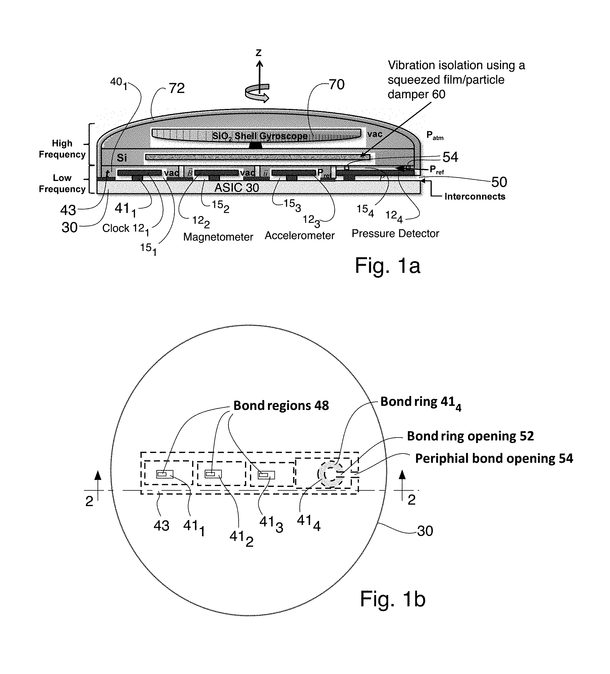
An INS typically includes accelerometers and gyroscopes for rotation and acceleration detection. The accuracy of an INS is improved with inclusion of additional sensors such as magnetometers and pressure sensors. MEMs integrated INS's presently combine and align these individually packaged sensors within an outer package housing to form a complete INS. An INS comprised of a clock, gyroscope, accelerometer, pressure sensor and magnetometer; typically requires different environments for the individual sensors, leading to increased size, complexity and cost of the composite unit.
In this invention, we describe an approach for monolithic integration of such sensors at the wafer level, yielding a composite system that is compact, low cost and while maintaining high stability and accuracy. We propose to package a sensor suite monolithically, such that each sensor component is sealed within in its required environment (eg vacuum, nitrogen, under pressure etc), via a monolithic process. Furthermore, sensor alignment is completed lithographically, eliminating the need for post processing alignment.
BRIEF DESCRIPTION OF THE INVENTION
In one aspect the present invention provides a sensor suite for an inertial navigation system in which several sensors are monolithically formed on a single wafer and where each sensor is sealed under a unique pressure and/or a unique gaseous material.
In another aspect the present invention provides a device comprising: a single IC wafer; a plurality of sensors bonded to bond regions on said single IC wafer, at least one of said bond regions including an opening therein in gaseous communication with a pressure chamber associated with at least one of the plurality of said sensors; and a plurality of caps encapsulating said plurality of sensors, at least one of said plurality of caps forming at least a portion of said pressure chamber.
In still another aspect the present invention provides a method of making a device comprising the steps of: temporarily bonding a handle wafer with a wafer from which sensors and/or devices are to be formed; forming said sensors and/or devices at least in part from said wafer; adhering exposed surfaces of said sensors and/or devices to bond regions on an integrated circuit chip or wafer; removing the handle wafer from the sensors and/or devices; and encapsulating the sensors and/or devices with a plurality of caps, each cap encapsulating one or more of said sensors and/or devices with a unique environment.
BRIEF DESCRIPTION OF THE DRAWINGS
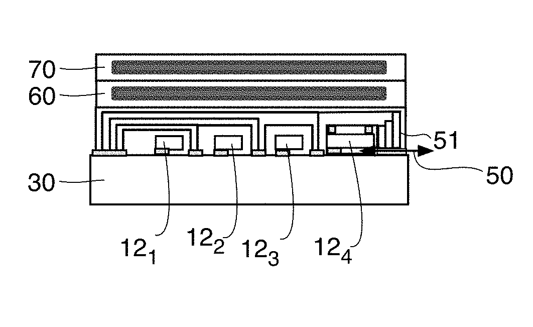
FIG. 1a is a side view schematic illustration of the monolithically formed INS showing sensor components sealed in individual environments and at specific required pressures, while FIG. 1b is a cross section view thereof.
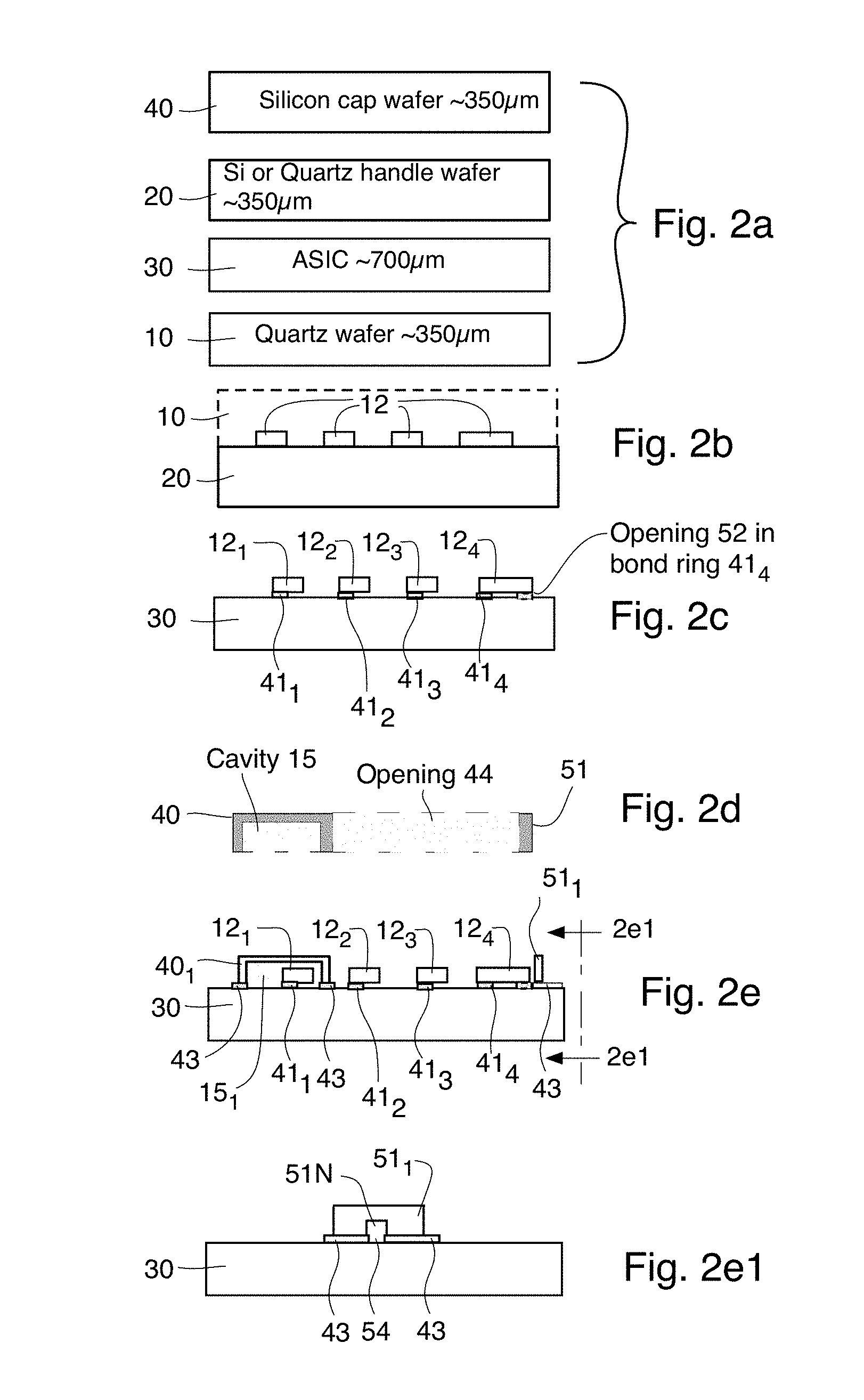
FIGS. 2a-2j are across view (taken along line 2-2 shown in FIG. 1b) showing the steps used in a method described herein to form a slightly modified embodiment of the monolithically formed INS depicted by FIG. 1a;
FIG. 2e1 is a side elevational view of the INS being formed at the step corresponding to FIG. 2e.
DETAILED DESCRIPTION
A schematic of the inertial navigation system (INS) is presented in FIG. 1a, in which components of the INS are preferably formed monolithically and then wafer bonded to enclose each sensor (or device) 12.sub.1-12.sub.4 of the INS in individual environments with individual cavities 15.sub.1-15.sub.4 using respective caps 40.sub.1-40.sub.4. In this way, the size of the composite unit is reduced and the alignment of the sensors (or devices) 12.sub.1-12.sub.4 within the system is also simplified since sensor alignment is achieved via lithographic wafer scale fabrication techniques and therefore post processing alignment can be eliminated. In order to discuss the construction of such an INS, the corresponding fabrication process flow is shown below in FIGS. 2a-2j. The sensors (or devices) are typically sensors (such as compasses, pressure detectors, magnetometers and/or accelerometers), but devices (such as electronic clocks) are sometimes also used in an INS and can be embodied in the INS using the same construction techniques as used with the sensors, as is described below.
Initially (see FIG. 2a) one begins with a quartz wafer 10, a quartz or silicon handle wafer 20, an Application Specific Integrated Circuit (ASIC) wafer 30 containing electronics and preferably as many silicon cap wafers 40.sub.1 . . . 40.sub.N as there are planned monolithic sensors 12.sub.1 . . . 12.sub.N to be formed from the quartz wafer 10. The embodiment of FIGS. 2a-2j has four sensors (or devices) three of which 12.sub.1 . . . 12.sub.3 are preferably totally encapsulated by an associated cap 40.sub.1 . . . 40.sub.3 in a hermetically sealed cavity 15.sub.1 . . . 15.sub.3 and one of which 12.sub.4 (a pressure detector) is partially encapsulated by cap 40.sub.4 and has an sealed cavity or pressure chamber 15.sub.4 associated with it for containing a gas at a reference pressure P.sub.ref. The pressure detector 12.sub.4 detects a differential pressure across a diaphragm, one side of which is exposed to that reference pressure P.sub.ref and the other side of which is preferably exposed to ambient pressure via a channel 50. The number and types of sensors and devices may be varied as needed to the use of any of them is optional.
The suggested initial thicknesses of these elements are identified on FIG. 2a but these thicknesses can be varied as needed or desired.
The quartz wafer 10 is temporarily bonded to the quartz or silicon handle wafer 20 (the quartz wafer 10 is shown in dashed lines in FIG. 2b) using a temporary adhesive, for example wax, (not shown) or a temporary fusion bond, followed by thinning and patterning of the quartz wafer 10 to define individual quartz sensors and/or devices 12 from quartz wafer 10 which are thus temporarily adhered to the quartz or silicon handle wafer 20 by the aforementioned temporary adhesive or fusion bond (or other temporary bonding technique). The individual quartz sensors and/or devices 12 of FIG. 2b are individually numbered 12.sub.1-12.sub.4 in the following figures. Four sensors and/or devices 12 are shown on FIG. 2b, but the number of sensors and/or devices 12 formed from the quartz wafer 10 may be varied as needed to accommodate the number needed in the sensor suite to be monolithically encapsulated.
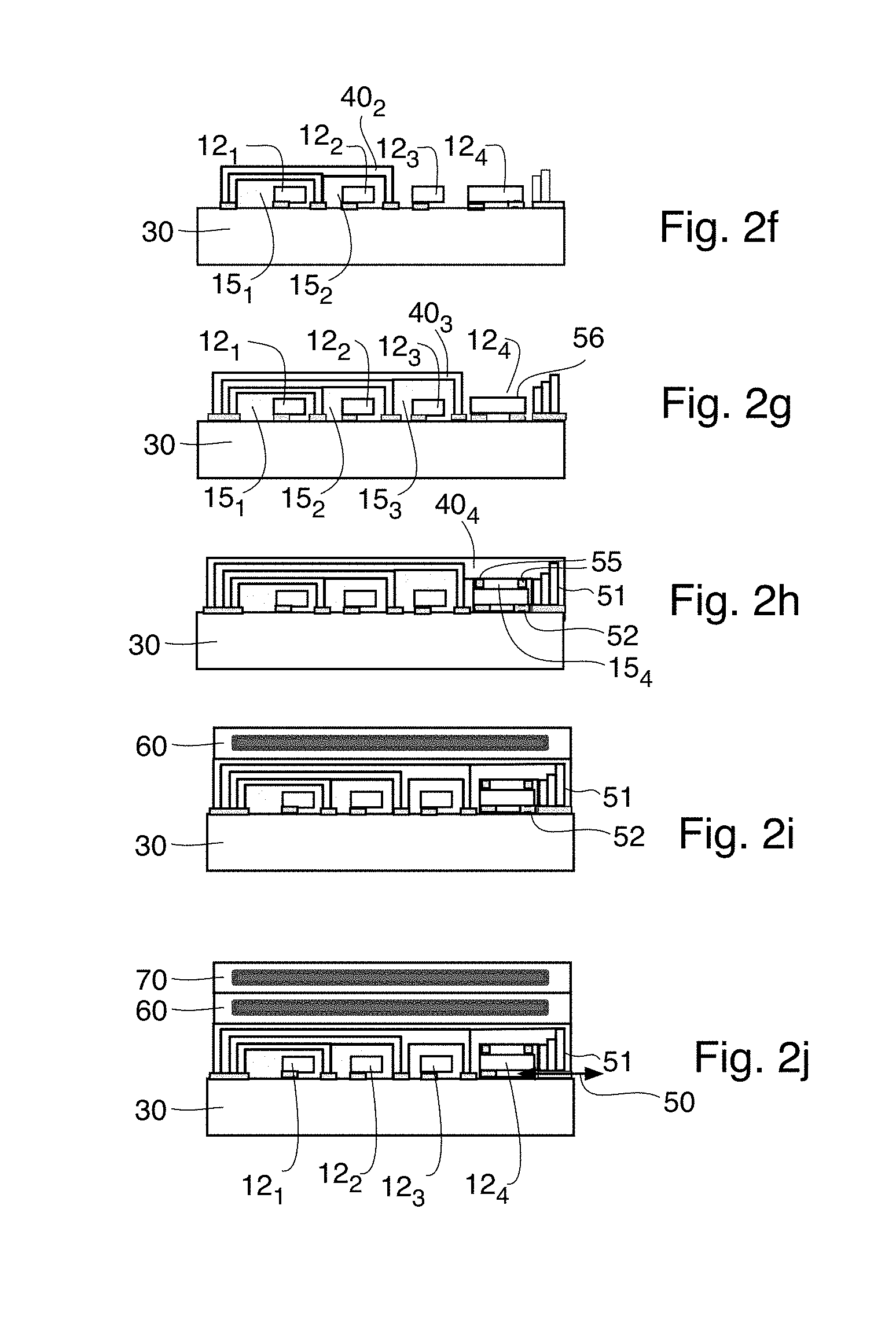
Next the sensors and/or devices 12 are bonded to the ASIC wafer 30 at bond regions 41.sub.1-41.sub.3 and at a ring bond 41.sub.4 preferably using a thermo-compression bond under vacuum. The temporary quartz or silicon handle wafer 20 is then preferably removed resulting in the structure depicted by FIG. 2c. One of the sensors is preferably a pressure sensor to sense ambient pressure and therefor an opening 52 in the bond ring 41.sub.4 is provided to allow pressure equalization for the pressure sensor, which in this embodiment is sensor 12.sub.4. See FIG. 1b.
Recall that there are preferably a number of silicon cap wafers 40 which is preferably less than or equal to the number of sensors to be encapsulated. If two sensors both require the same ambient conditions then they may potentially share a common sealed cavity 15. In this embodiment four sensors are encapsulated individually and thus four silicon cap wafers 40 are utilized. Each of the cap wafers 40 is patterned with an appropriate cavity 15 and appropriate opening(s) 44 to seal individual sensors in particular environments needed by the individual sensor. FIG. 2d shows a cap wafer 40 with a single cavity 15 and an opening 44 therein (located between the cavity 15 and an end wall 51) positioned so that when this particular cap wafer 40 is applied to the structure depicted by FIG. 2c, the cavity 15 therein will cover and seal the left most sensor (or device) 12.sub.1 shown in FIG. 2c and leave the remaining sensors (or devices) 12.sub.2-12.sub.4 exposed through opening 44. Cavities 15 define the sealing environment (encapsulation) for typically a single sensor (or device) as each successive patterned cap wafer 40 is bonded into position on the ASIC wafer 30. The openings or holes 44 allow for a different environment when encapsulating of the other devices or sensors 12. The first sensor (or device) 12.sub.1 (a quartz clock, for example, in the embodiment of FIG. 1a) is sealed at some desired gas pressure P.sub.1 in a desired gas G.sub.1 through the bonding of the first patterned cap wafer 40.sub.1 to the ASIC wafer 30 at bond 43 forming the hermetically sealed cavity 15.sub.1 as shown in FIG. 2e.
In FIG. 2e the height of the bond regions 41.sub.1-41.sub.4 for the four sensors (or devices) 12.sub.1-12.sub.4 in this embodiment and the height of the peripheral bond region 43 for the four cap wafers 40.sub.1-40.sub.4 in this embodiment are exaggerated for ease of illustration. The peripheral bond region 43 is also shown in FIG. 1b by dashed lines. The peripheral bond region 43 preferably completely encircles each of the four sensors or devices 12.sub.1-12.sub.4 except the last one (12.sub.4) which is a preferably an ambient pressure detector and therefor needs a path 50 to ambient air. Therefore the pressure detector 12.sub.4 is only partially encircled by the peripheral bond region 43 in that there is preferably a break or opening in bond region 43 labeled by numeral 54. The end walls 51 of the four cap wafers 40.sub.1-40.sub.4 each also preferably has an opening or notch 51N therein to provide the path 50 to ambient air from sensor 12.sub.4 through opening 52 and through the openings 54 and/or notches 51N.
After the first sensor (or device) 12.sub.1 encapsulated within its cavity of cap wafer 40.sub.1, the second sensor 12.sub.2 (a quartz magnetometer, for example, in the embodiment of FIG. 1a) is then encapsulated at a gas pressure P.sub.2 in ambient gas G.sub.2 with the second patterned cap wafer 40.sub.2 at the peripheral bond 43 as shown in FIG. 2f. This process with successive cap wafers 40 (each with suitable cavities 15 and openings 44 defined therein) continues with the remaining sensors and cap wafers at their required environmental conditions being encapsulated preferably as shown by FIGS. 2g and 2h and bonded to layer 30 at, for example, bond the peripheral bond 43. The encapsulated pressure (P.sub.1, P.sub.2, etc.) may be 0, i.e., a vacuum and the gases G.sub.1, and G.sub.2, etc., if used, are preferably nitrogen and/or helium. The same gas (or a common vacuum) be used in two different encapsulations. So each encapsulated environment may have its own unique gas type and pressure, but, if desired, neighboring sensors or devices can share a unique gas type and pressure if desired.
In FIGS. 2f-2h each cap wafer 40 not only encapsulates a single sensor (or device) 12 with a desired gas at a desired pressure, but also re-encapsulates the previously encapsulated sensors (or devices) 12. Instead of having each successive cap wafer 40 re-encapsulate prior encapsulation(s), each successive cap wafer 40 may be formed instead to encapsulate only its associated sensor without also encapsulating any previous encapsulations as shown in FIG. 1a. Of course, various combinations of these two encapsulation techniques will suggest themselves to those skilled in the art.
The bonds 41.sub.1-41.sub.4 and 43 are preferably formed as a thermo-compression metal bond but other bond techniques could alternatively be used especially if the bonds need to be made at lower than usual temperatures for thermo-compression bonding due to, for example, a temperature sensitivity of one or more of the sensors. The stoichiometry of the bonds 43 for each of the cap wafers 40 is preferably selected to achieve a hermetic seal of the encapsulated sensors 12.sub.1-12.sub.3 within cavities 15.
The fourth device 12.sub.4 in this embodiment is preferably a pressure sensor which has a diaphragm 56 (see FIG. 2g) which is sealed around its perimeter by a perimeter seal 55 from above to define the cavity or chamber 15.sub.4 which preferably formed at the reference pressure of P.sub.ref. Below the diaphragm 56 is located a air path 50 (see also FIG. 2e1) to ambient in the form of the missing segment 52 of the bond metal ring 41.sub.4 and the missing portion 54 in the peripheral bond 43 in combination with opening(s) and/or notch(es) 51N allows equalization of the pressure under the diaphragm 56 with the ambient pressure to be measured via the air path 50.
The pressure sensor 12.sub.4 of this embodiment measures a differential pressure difference across diaphragm 56. On one side of the diaphragm 56, the pressure is well defined (at a reference pressure P.sub.ref) by the capping process of cap wafer 40.sub.4 under a controlled environment (gas and pressure) at seals 54. Alternatively, the damping unit 60 may be used as the final cap (see FIG. 1a). The final cap wafer 40.sub.4 in the embodiment of FIG. 2h utilizes a seal 54 at the edge of the cavity 15.sub.4 thereby locking in that controlled environment between the diaphragm 56 and the cap. On the other side of the diaphragm 56, the gap or opening 52 in the seal ring 41.sub.4 allows pressure to equalize to ambient pressure (via passage 50), which is the pressure to be measured.
Vibration isolation is desirable for many sensors and therefore a silicon wafer containing a vibration damping unit 60 is preferably bonded (see FIG. 2i) to the topmost cap 40 of the capped wafer stack shown in FIG. 2h. The vibration damping unit 60 may utilize a squeezed film or particles as the damping agent. The final component is preferably a gyroscope 70 which is bonded to the top of the vibration damping unit 60 (see FIG. 2j) to complete the encapsulation of the inertial navigation system. The vibration damping unit 60 is preferably bonded to the composite unit depicted in FIG. 2h providing a vibration-damped surface for receiving the gyroscope 70. The gyroscope 70 is mounted on the the vibration damping unit 60. The vibration damping unit 60 may be fabricated using standard MEMS fabrications techniques. Preferred materials for the composite unit include semiconductors (silicon, etc.), dielectrics (silicon dioxide, silicon nitride, etc.), metals (aluminum, gold, titanium, etc.) and polymers (polyamide, etc.).
The vibration damping unit 60 in some embodiments may be located under the ASIC wafer 30 (as viewed in FIG. 1a) instead of (or in addition to) on top of the encapsulated sensors 12 if none of the sensors is an accelerometer, for example.
The gyroscope 70, the damper 60 and the sensors 12 may be all enclosed within a rounded shell 72 as depicted by FIG. 1a if desired. Of course, the shell 72 may assume some other geometric shape (square, rectangular, etc.).
As can be seen with reference to FIG. 1a, sensor or device 12.sub.1 may serve as a resonator for a clock, while sensor or device 12.sub.2 may be magnetometer while sensor or device 12.sub.3 may be an accelerometer in order to form an INS as mentioned above. The sensors and devices 12.sub.1-12.sub.4 may perform other or additional tasks if desired.
This method may utilize quartz processing techniques described in U.S. Pat. No. 7,237,315 to make quartz based sensors 12.
This concludes the description of embodiments of the present invention. The foregoing description of these embodiments and methods of making same have been presented for the purposes of illustration and description. It is not intended to be exhaustive or to limit the invention to the precise form or methods disclosed. Many modifications and variations are possible in light of the above teachings. It is intended that the scope of the invention be limited not by this detailed description, but rather by the claims appended hereto.
* * * * *
D00000
D00001
D00002
D00003
XML
uspto.report is an independent third-party trademark research tool that is not affiliated, endorsed, or sponsored by the United States Patent and Trademark Office (USPTO) or any other governmental organization. The information provided by uspto.report is based on publicly available data at the time of writing and is intended for informational purposes only.
While we strive to provide accurate and up-to-date information, we do not guarantee the accuracy, completeness, reliability, or suitability of the information displayed on this site. The use of this site is at your own risk. Any reliance you place on such information is therefore strictly at your own risk.
All official trademark data, including owner information, should be verified by visiting the official USPTO website at www.uspto.gov. This site is not intended to replace professional legal advice and should not be used as a substitute for consulting with a legal professional who is knowledgeable about trademark law.