Method of forming a power module with a magnetic device having a conductive clip
Lotfi , et al.
U.S. patent number 10,304,615 [Application Number 14/220,478] was granted by the patent office on 2019-05-28 for method of forming a power module with a magnetic device having a conductive clip. This patent grant is currently assigned to Enpirion, Inc.. The grantee listed for this patent is Enpirion, Inc.. Invention is credited to Trifon M. Liakopoulos, Ashraf W. Lotfi, John D. Weld, Mathew A. Wilkowski.


| United States Patent | 10,304,615 |
| Lotfi , et al. | May 28, 2019 |
Method of forming a power module with a magnetic device having a conductive clip
Abstract
A method of forming a power module located on a conductive substrate by providing power conversion circuitry. The method of providing the power conversion circuitry includes forming a magnetic device by placing a magnetic core proximate a conductive substrate with a surface thereof facing a conductive substrate, and placing a conductive clip proximate a surface of the magnetic core. The method of forming the magnetic device also includes electrically coupling ends of the conductive clip to the conductive substrate to cooperatively form a winding therewith about the magnetic core. The method of providing the power conversion circuitry also includes providing at least one switch on the conductive substrate. The method of forming the power module also includes depositing an encapsulant about the power conversion circuitry.
| Inventors: | Lotfi; Ashraf W. (Bridgewater, NJ), Wilkowski; Mathew A. (Nazareth, PA), Liakopoulos; Trifon M. (Bridgewater, NJ), Weld; John D. (Ledgewood, NJ) | ||||||||||
|---|---|---|---|---|---|---|---|---|---|---|---|
| Applicant: |
|
||||||||||
| Assignee: | Enpirion, Inc. (Hampton,
NJ) |
||||||||||
| Family ID: | 37900566 | ||||||||||
| Appl. No.: | 14/220,478 | ||||||||||
| Filed: | March 20, 2014 |
Prior Publication Data
| Document Identifier | Publication Date | |
|---|---|---|
| US 20140203903 A1 | Jul 24, 2014 | |
Related U.S. Patent Documents
| Application Number | Filing Date | Patent Number | Issue Date | ||
|---|---|---|---|---|---|
| 11243787 | Oct 5, 2005 | 8701272 | |||
| Current U.S. Class: | 1/1 |
| Current CPC Class: | H01F 17/04 (20130101); H01F 27/2847 (20130101); H02M 3/00 (20130101); H01L 23/495 (20130101); H01L 25/16 (20130101); H01L 2224/49052 (20130101); H01L 2224/48247 (20130101); Y10T 29/49073 (20150115); H01L 2924/19107 (20130101); H01L 2924/01015 (20130101); H01L 2924/19105 (20130101); H01L 2924/00014 (20130101); Y10T 29/49076 (20150115); Y10T 29/49121 (20150115); H01L 2224/49096 (20130101); H01F 2027/2814 (20130101); H01L 2224/45144 (20130101); H01L 2924/14 (20130101); H01L 2224/49175 (20130101); H01L 24/45 (20130101); Y10T 29/4902 (20150115); H01L 24/48 (20130101); H01L 2924/00011 (20130101); H01L 2924/10253 (20130101); Y10T 29/49146 (20150115); H01L 2224/45147 (20130101); H01L 24/49 (20130101); H01L 2924/01047 (20130101); H01L 2224/49171 (20130101); H01L 2924/10253 (20130101); H01L 2924/00 (20130101); H01L 2924/01047 (20130101); H01L 2924/00 (20130101); H01L 2224/45147 (20130101); H01L 2924/00 (20130101); H01L 2224/45144 (20130101); H01L 2924/00014 (20130101); H01L 2924/01015 (20130101); H01L 2924/00 (20130101); H01L 2924/00014 (20130101); H01L 2224/05599 (20130101); H01L 2924/14 (20130101); H01L 2924/00 (20130101); H01L 2924/00011 (20130101); H01L 2924/01033 (20130101) |
| Current International Class: | H01F 27/24 (20060101); H01L 23/495 (20060101); H01F 17/04 (20060101); H01F 27/29 (20060101); H01F 27/02 (20060101); H01L 25/16 (20060101); H02M 3/00 (20060101); H01F 27/28 (20060101); H01L 23/00 (20060101) |
| Field of Search: | ;336/221,192,200 |
References Cited [Referenced By]
U.S. Patent Documents
| 1889398 | November 1932 | Bishop |
| 2600473 | June 1952 | Brockman |
| 3210707 | October 1965 | Constantakes |
| 3691497 | September 1972 | Bailey et al. |
| 3762039 | October 1973 | Douglass |
| 3902148 | August 1975 | Drees et al. |
| 3908264 | September 1975 | Friberg et al. |
| 3947699 | March 1976 | Whitmer |
| 4101389 | July 1978 | Uedaira |
| 4103267 | July 1978 | Olschewski |
| 4187128 | February 1980 | Billings et al. |
| 4199743 | April 1980 | Martincic |
| 4433927 | February 1984 | Cavallari |
| 4538118 | August 1985 | Lorieux |
| 4586436 | May 1986 | Denney et al. |
| 4636752 | January 1987 | Saito |
| 4668310 | May 1987 | Kudo et al. |
| 4681718 | July 1987 | Oldham |
| 4751199 | June 1988 | Phy |
| 4754317 | June 1988 | Comstock et al. |
| 4777465 | October 1988 | Meinel |
| 4808118 | February 1989 | Wilson et al. |
| 4847986 | July 1989 | Meinel |
| 4870224 | September 1989 | Smith et al. |
| 4916522 | April 1990 | Cohn |
| 4975671 | December 1990 | Dirks |
| 5056214 | October 1991 | Holt |
| 5059278 | October 1991 | Cohen et al. |
| 5096513 | March 1992 | Sawa et al. |
| 5118298 | June 1992 | Murphy |
| 5161098 | November 1992 | Balakrishnan |
| 5187119 | February 1993 | Cech et al. |
| 5262296 | November 1993 | Ogawa et al. |
| 5279988 | January 1994 | Saadat et al. |
| 5285369 | February 1994 | Balakrishnan |
| 5345670 | September 1994 | Pitzele et al. |
| 5351167 | September 1994 | Wai |
| 5353001 | October 1994 | Meinel |
| 5428245 | June 1995 | Lin |
| 5436409 | July 1995 | Sawada et al. |
| 5469334 | November 1995 | Balakrishnan |
| 5484494 | January 1996 | Oda et al. |
| 5524334 | June 1996 | Boesel |
| 5561438 | October 1996 | Nakazawa |
| 5574273 | November 1996 | Nakagawa et al. |
| 5574420 | November 1996 | Roy |
| 5578261 | November 1996 | Manzione et al. |
| 5692296 | December 1997 | Variot |
| 5783025 | July 1998 | Hwang et al. |
| 5787569 | August 1998 | Lotfi et al. |
| 5788854 | August 1998 | Desaigoudar et al. |
| 5802702 | September 1998 | Fleming et al. |
| 5807959 | September 1998 | Wu et al. |
| 5834691 | November 1998 | Aoki |
| 5835350 | November 1998 | Stevens |
| 5837155 | November 1998 | Inagaki et al. |
| 5846441 | December 1998 | Roh |
| 5898991 | May 1999 | Fogel et al. |
| 5920249 | July 1999 | Huss |
| 5973923 | October 1999 | Jitaru |
| 5998925 | December 1999 | Shimizu et al. |
| 6005377 | December 1999 | Chen et al. |
| 6005467 | December 1999 | Abramov |
| 6060176 | May 2000 | Semkow et al. |
| 6081997 | July 2000 | Chia et al. |
| 6087920 | July 2000 | Abramov |
| 6087921 | July 2000 | Morrison |
| 6094123 | July 2000 | Roy |
| 6101218 | August 2000 | Nagano |
| 6118351 | September 2000 | Kossives et al. |
| 6118360 | September 2000 | Neff |
| 6160721 | December 2000 | Kossives et al. |
| 6204745 | March 2001 | Liu |
| 6255714 | July 2001 | Kossives et al. |
| 6317948 | November 2001 | Kola et al. |
| 6353379 | March 2002 | Busletta et al. |
| 6362714 | March 2002 | Rice |
| 6366486 | April 2002 | Chen et al. |
| 6440750 | August 2002 | Feygenson et al. |
| 6448640 | September 2002 | Corisis |
| 6466454 | October 2002 | Jitaru |
| 6479981 | November 2002 | Schweitzer, Jr. et al. |
| 6495019 | December 2002 | Filas et al. |
| 6541819 | April 2003 | Lotfi et al. |
| 6549409 | April 2003 | Saxelby, Jr. et al. |
| 6552629 | April 2003 | Dixon et al. |
| 6578253 | June 2003 | Herbert |
| 6608332 | August 2003 | Shimizu et al. |
| 6624498 | September 2003 | Filas et al. |
| 6649422 | November 2003 | Kossives et al. |
| 6691398 | February 2004 | Gutierrez |
| 6693805 | February 2004 | Steigerwald et al. |
| 6731002 | May 2004 | Choi |
| 6747538 | June 2004 | Kuwata et al. |
| 6757174 | June 2004 | Nagai |
| 6790379 | September 2004 | Aoki et al. |
| 6808807 | October 2004 | Anand et al. |
| 6912781 | July 2005 | Morrison et al. |
| 6922130 | July 2005 | Okamoto |
| 6989121 | January 2006 | Thummel |
| 6998952 | February 2006 | Zhou et al. |
| 7015544 | March 2006 | Lotfi et al. |
| 7019505 | March 2006 | Dwarakanath et al. |
| 7020295 | March 2006 | Hamada et al. |
| 7021518 | April 2006 | Kossives et al. |
| 7023315 | April 2006 | Yeo et al. |
| 7038438 | May 2006 | Dwarakanath et al. |
| 7057486 | June 2006 | Kiko |
| 7101737 | September 2006 | Cobbley |
| 7175718 | February 2007 | Nobutoki et al. |
| 7180395 | February 2007 | Lotfi et al. |
| 7214985 | May 2007 | Lotfi et al. |
| 7229886 | June 2007 | Lotfi et al. |
| 7230302 | June 2007 | Lotfi et al. |
| 7230316 | June 2007 | Yamazaki et al. |
| 7232733 | June 2007 | Lotfi et al. |
| 7236086 | June 2007 | Vinciarelli et al. |
| 7244994 | July 2007 | Lotfi et al. |
| 7250842 | July 2007 | Johnson et al. |
| 7256674 | August 2007 | Lotfi et al. |
| 7276998 | October 2007 | Lotfi et al. |
| 7330017 | February 2008 | Dwarakanath et al. |
| 7426780 | September 2008 | Lotfi et al. |
| 7434306 | October 2008 | Gardner |
| 7462317 | December 2008 | Lotfi et al. |
| 7498522 | March 2009 | Itoh |
| 7521907 | April 2009 | Cervera et al. |
| 7544995 | June 2009 | Lotfi et al. |
| 7642762 | January 2010 | Xie et al. |
| 7688172 | March 2010 | Lotfi et al. |
| 7786837 | August 2010 | Hebert |
| 7791440 | September 2010 | Ramadan et al. |
| 7876572 | January 2011 | Sota |
| 7920042 | April 2011 | Lotfi et al. |
| 7936160 | May 2011 | Sheehan |
| 7948772 | May 2011 | Tung et al. |
| 7952459 | May 2011 | Lotfi et al. |
| 7955868 | June 2011 | Lotfi et al. |
| 7974103 | July 2011 | Lim et al. |
| 8018315 | September 2011 | Lotfi et al. |
| 8043544 | October 2011 | Lotfi et al. |
| 2001/0030595 | October 2001 | Hamatani et al. |
| 2001/0041384 | November 2001 | Ohgiyama et al. |
| 2002/0067234 | June 2002 | Kung |
| 2002/0153258 | October 2002 | Filas et al. |
| 2003/0062541 | April 2003 | Warner |
| 2003/0076662 | April 2003 | Miehling |
| 2003/0232196 | December 2003 | Anand et al. |
| 2004/0130428 | July 2004 | Mignano et al. |
| 2004/0150500 | August 2004 | Kiko |
| 2004/0263309 | December 2004 | Ito |
| 2005/0011672 | January 2005 | Alawani et al. |
| 2005/0052267 | March 2005 | Singu |
| 2005/0167756 | August 2005 | Lotfi et al. |
| 2005/0168203 | August 2005 | Dwarakanath et al. |
| 2005/0168205 | August 2005 | Dwarakanath et al. |
| 2005/0169024 | August 2005 | Dwarakanath et al. |
| 2005/0212132 | September 2005 | Hsuan et al. |
| 2006/0009023 | January 2006 | Nair et al. |
| 2006/0038225 | February 2006 | Lotfi et al. |
| 2006/0040449 | February 2006 | Lotfi et al. |
| 2006/0040452 | February 2006 | Lotfi et al. |
| 2006/0081937 | April 2006 | Lotfi et al. |
| 2006/0096087 | May 2006 | Lotfi et al. |
| 2006/0096088 | May 2006 | Lotfi et al. |
| 2006/0097831 | May 2006 | Lotfi et al. |
| 2006/0097832 | May 2006 | Lotfi et al. |
| 2006/0097833 | May 2006 | Lotfi et al. |
| 2006/0109071 | May 2006 | Thongsouk |
| 2006/0109072 | May 2006 | Giandalia et al. |
| 2006/0145800 | July 2006 | Dadafshar et al. |
| 2006/0197207 | September 2006 | Chow et al. |
| 2007/0025092 | February 2007 | Lee et al. |
| 2007/0074386 | April 2007 | Lotfi et al. |
| 2007/0075815 | April 2007 | Lotfi et al. |
| 2007/0075816 | April 2007 | Lotfi et al. |
| 2007/0075817 | April 2007 | Lotfi et al. |
| 2007/0246808 | October 2007 | Ewe et al. |
| 2008/0001701 | January 2008 | Gardner et al. |
| 2008/0090079 | April 2008 | Fajardo et al. |
| 2008/0258274 | October 2008 | Sinaga et al. |
| 2008/0258278 | October 2008 | Ramos et al. |
| 2008/0301929 | December 2008 | Lotfi et al. |
| 2008/0303131 | December 2008 | McElrea et al. |
| 2009/0004774 | January 2009 | Lee et al. |
| 2009/0057822 | March 2009 | Wen et al. |
| 2009/0065964 | March 2009 | Lotfi et al. |
| 2009/0068347 | March 2009 | Lotfi et al. |
| 2009/0146297 | June 2009 | Badakere et al. |
| 2010/0084750 | April 2010 | Lotfi et al. |
| 2010/0087036 | April 2010 | Lotfi et al. |
| 2010/0164449 | July 2010 | Dwarakanath et al. |
| 2010/0164650 | July 2010 | Abou-Alfotouh et al. |
| 2010/0212150 | August 2010 | Lotfi et al. |
| 2010/0214746 | August 2010 | Lotfi et al. |
| 2011/0181383 | July 2011 | Lotfi et al. |
| 10022980 | Dec 2000 | DE | |||
| 2 041 818 | Sep 1980 | GB | |||
| 402228013 | Sep 1990 | JP | |||
| 5-314885 | Nov 1993 | JP | |||
| 6-251958 | Sep 1994 | JP | |||
Other References
|
Betancourt-Zamora, R.J., et al., "A 1.5 mW, 200 MHz CMOS VCO for Wireless Biotelemetry," First International Workshop on Design of Mixed-Mode Integrated Circuits and Applications, Jul. 1997, pp. 72-74, Cancun, Mexico. cited by applicant . Goodman, J., et al., "An Energy/Security Scalable Encryption Processor Using an Embedded Variable Voltage DC/DC Converter," IEEE Journal of Solid-State Circuits, Nov. 1998, pp. 1799-1809, vol. 33, No. 11, IEEE, Los Alamitos, CA. cited by applicant . Horowitz, P., et al., "The Art of Electronics," Second Edition, 1989, Chapter 5: Active Filters and Oscillators, pp. 288-291, Cambridge University Press, Cambridge, MA. cited by applicant . Lotfi, A.W., et al., "Issues and Advances in High-Frequency Magnetics for Switching Power Supplies," Proceedings of the IEEE, Jun. 2001, pp. 833-845, vol. 89, No. 6, IEEE, Los Alamitos, CA. cited by applicant . Sato, M., et al., "Influences of Molding Conditions on Die-pad Behavior in IC Encapsulation Process Analyzed by Hall Element Method," IEEE Transactions on Advanced Packaging, Aug. 2000, pp. 574-581, vol. 23, No. 3, IEEE, Los Alamitos, CA. cited by applicant . "Technical Specification: PMF 8000 Series: POL Regulator, Input 10.8-13.2 V, Output 10 A/55 W," EN/LZT 146 318 R1C, Sep. 2006, pp. 1-47, Ericsson Power Modules AB, Stockholm, Sweden. cited by applicant. |
Primary Examiner: Enad; Elvin G
Assistant Examiner: Hossain; Kazi S
Attorney, Agent or Firm: Fletcher Yoder P.C.
Parent Case Text
This application is a continuation of U.S. patent application Ser. No. 11/243,787, entitled "Method of Forming a Power Module with a Magnetic Device Having a Conductive Clip", filed on Oct. 5, 2005. The above-listed application is commonly assigned with the present invention and is incorporated herein by reference as if reproduced herein in its entirety.
Claims
What is claimed is:
1. A magnetic device, comprising: a magnetic core, including: a first surface continuously spanning an end-to-end boundary of said magnetic core and facing a first conductive substrate; and an opposing second surface continuously spanning said end-to-end boundary of said magnetic core; a first u-shaped conductive clip facing said second surface and continuously spanning said end-to-end boundary of said magnetic core to form a first portion of a winding of said magnetic device; and a second u-shaped conductive clip facing said second surface and continuously spanning said end-to-end boundary of said magnetic core to form a second portion of said winding of said magnetic device, wherein said first u-shaped conductive clip is coupled by a first solder area to said first conductive substrate, and said second u-shaped conductive clip is coupled by a second solder area to a second conductive substrate separate from said first conductive substrate, and wherein a first location on said first conductive substrate where said first u-shaped conductive clip is coupled to said first conductive substrate by the first solder area and a second location on said second conductive substrate where said second u-shaped conductive clip is coupled to said second conductive substrate by the second solder area are separated by a gap, wherein the gap comprises an air gap between the first solder area and the second solder area.
2. The magnetic device as recited in claim 1 wherein ends of said first and second u-shaped conductive clips are electrically coupled to said first and second conductive substrates to cooperatively form said winding therewith about said magnetic core.
3. The magnetic device as recited in claim 1 wherein ends of said first and second u-shaped conductive clips are bent toward said first and second conductive substrates about ends of said magnetic core.
4. The magnetic device as recited in claim 1 wherein said first and second conductive substrates also form an electrically conductive interconnect layer for a component coupled thereto.
5. The magnetic device as recited in claim 1 wherein said first and second conductive substrate also form an electrically conductive interconnect layer for a component wire bonded thereto.
6. The magnetic device as recited in claim 1 wherein said magnetic device is an inductor.
7. The magnetic device as recited in claim 1 wherein said first and second conductive substrates comprise a conductive leadframe.
8. The magnetic device as recited in claim 7 wherein said conductive leadframe includes leadframe fingers that form terminals for external electrical connections.
9. The magnetic device as recited in claim 1 further comprising an additional gap between said second surface of said magnetic core and said second u-shaped conductive clip.
10. The magnetic device as recited in claim 1 wherein said first surface of said magnetic core is adhered to an adhesive on said first conductive substrate.
11. The magnetic device as recited in claim 1 wherein said first surface of said magnetic core is soldered to said first conductive substrate.
12. The magnetic device as recited in claim 1 wherein said first or second u-shaped conductive clip is about 8 to 12 millimeters (mils) in thickness.
13. The magnetic device as recited in claim 1 wherein said magnetic core is formed from manganese zinc ferrite.
14. The magnetic device as recited in claim 1 wherein said magnetic core is formed from a bar of magnetic material.
15. The magnetic device as recited in claim 1 wherein said magnetic core is a single piece magnetic core.
16. The magnetic device as recited in claim 1 further comprising an encapsulant about said magnetic device.
17. A magnetic device, comprising: a magnetic core, including: a first surface continuously spanning an end-to-end boundary of said magnetic core and facing a first conductive substrate; and an opposing second surface continuously spanning said end-to-end boundary of said magnetic core; a first u-shaped conductive clip facing said second surface and continuously spanning end-to-end boundary of said magnetic core to form a first portion of a winding of said magnetic device; a second u-shaped conductive clip facing said second surface and continuously spanning said end-to-end boundary of said magnetic core to form a second portion of said winding of said magnetic device, wherein said first u-shaped conductive clip is coupled by a first solder area to said first conductive substrate, and said second u-shaped conductive clip is coupled by a second solder area to a second conductive substrate separate from said first conductive substrate, and wherein a first location on said first conductive substrate where said first u-shaped conductive clip is coupled to said first conductive substrate by the first solder area and a second location on said second u-shaped conductive substrate where said second u-shaped conductive clip is coupled to said second conductive substrate are separated by a gap, wherein the gap comprises an air gap between the first solder area and the second solder area; and a plurality of wire bonds coupled between said first conductive substrate and a semiconductor die.
18. A magnetic device, comprising: a magnetic core, including: a first surface continuously spanning an end-to-end boundary of said magnetic core and facing a first conductive substrate; and an opposing second surface continuously spanning said end-to-end boundary of said magnetic core; a first conductive clip facing said second surface and continuously spanning said end-to-end boundary of said magnetic core to form a first portion of a winding of said magnetic device; a second conductive clip facing said second surface and continuously spanning said end-to-end boundary of said magnetic core to form a second portion of said winding of said magnetic device, wherein said first conductive clip is coupled by a first solder area to said first conductive substrate, and said second conductive clip is coupled by a second solder area to a second conductive substrate separate from said first conductive substrate, and wherein a first location on said first conductive substrate where said first conductive clip is coupled to said first conductive substrate and a second location on said first conductive substrate where said second conductive clip is coupled to said second conductive substrate are separated by a gap, wherein the gap comprises an air gap between the first solder area and the second solder area; a plurality of wire bonds coupled between said first conductive substrate and a semiconductor die; and at least one wire bond coupled between said first conductive substrate and second conductive substrate.
Description
TECHNICAL FIELD
The present invention is directed, in general, to electronic devices and, in particular, to magnetic devices and power modules, and related methods of forming the same.
BACKGROUND
Magnetic devices such as inductors are often used in circuit design for electronic devices (e.g., power modules) in which energy is stored in a magnetic field surrounding an electrically conductive element such as a coil of copper wire. To produce an inductor that can store a useful amount of energy for a given size and a given current level, a number of electrically conductive turns or wires are formed around a magnetic structure or core such as a layer of magnetic material. The magnetic field is enhanced by the permeability of the magnetic material and by the presence of the multiple conductive turns. As the size of electronic devices has been reduced by using integrated circuits and printed wiring boards with surface mount assembly techniques, the size of inductors has not, to date, decreased proportionately.
Attempts to use finer wire sizes have resulted in inductor designs with limited current handling capability. Silver is recognized as a slightly better conductor than copper for higher current levels, but its expense is generally not warranted in practical products. These effects have combined to make the design of magnetic devices a continuing object for further size and cost reductions without compromising the respective current ratings.
A number of approaches beyond the use of finer copper wire have been used in the past to produce smaller inductors. For instance, U.S. Pat. No. 6,094,123 entitled "Low Profile Surface Mount Chip Inductor," to Apurba Roy, issued Jul. 25, 2000 and U.S. Pat. No. 5,802,702 entitled "Method of Making a Device including a Metallized Magnetic Substrate," to Fleming, et al., issued Sep. 8, 1998, which are incorporated herein by reference, disclose magnetic devices that form recesses in a bar of magnetic material for conductors and deposit conductive material in the recesses. Additionally, U.S. Pat. No. 5,574,420 entitled "Low Profile Surface Mounted Magnetic Devices and Components Therefor," to Roy, et al., issued Nov. 12, 1996, which is incorporated by reference, discloses a magnetic device that forms conductive pathways in a body of magnetic material, adds windings by inserting staple-like conductive piece parts through apertures in the body, and solders the staples to a patterned printed wiring board placed below a ceramic magnetic bar to complete the winding structure. Each of the magnetic devices disclosed in the aforementioned references suffer from a current limitation therefor, which is an impractical design and manufacturing approach for a mass market. The aforementioned magnetic devices also provide inadequate heat dissipation capability or reduction in the size thereof.
Thus, the designs for the magnetic devices in the past are inadequate to produce a sufficiently miniaturized magnetic device with a substantial current rating for application in compact devices such as high density power converters embodied in power modules. The power converters often employ magnetic devices that can sustain currents exceeding one ampere and are operable at switching frequencies that exceed one megahertz. Additionally, the magnetic devices should exhibit very low electrical resistance at the switching frequency and should be more compact than presently achievable designs. The design of power converters is inadequately served by these aforementioned limitations of present magnetic devices. In addition, a magnetic device integrable with manufacturing processes of the commensurate end product such as a power module would provide substantial cost savings therefor.
Accordingly, what is needed in the art is a magnetic device, and related method of forming the same, that can meet the more stringent requirements of present applications such as compact, efficient and high density power modules, while being manufacturable at high volume and with lower cost than is achieved with the prior art.
SUMMARY OF THE INVENTION
These and other problems are generally solved or circumvented, and technical advantages are generally achieved, by advantageous embodiments of the present invention which includes a method of forming a power module located on a conductive substrate by providing power conversion circuitry. The method of providing the power conversion circuitry includes forming a magnetic device by placing a magnetic core proximate a conductive substrate with a surface thereof facing a conductive substrate, and placing a conductive clip proximate a surface of the magnetic core. The method of forming the magnetic device also includes electrically coupling ends of the conductive clip to the conductive substrate to cooperatively form a winding therewith about the magnetic core. The method of providing the power conversion circuitry also includes providing at least one switch on the conductive substrate. The method of forming the power module also includes depositing an encapsulant about the power conversion circuitry.
In another aspect, the present invention provides a method of forming a power module located on a patterned, conductive leadframe, including providing power conversion circuitry. The method of forming the power conversion circuitry includes forming a magnetic device by adhering a magnetic core formed from a bar of magnetic material to the conductive leadframe, locating at least one conductive clip above the magnetic core, and soldering ends of the at least one conductive clip to the conductive leadframe to cooperatively form a winding therewith about the magnetic core. The method of forming the power conversion circuitry also includes providing at least one switch on the conductive leadframe. The method of forming the power module also includes depositing an encapsulant about the power conversion circuitry.
The foregoing has outlined rather broadly the features and technical advantages of the present invention in order that the detailed description of the invention that follows may be better understood. Additional features and advantages of the invention will be described hereinafter which form the subject of the claims of the invention. It should be appreciated by those skilled in the art that the conception and specific embodiment disclosed may be readily utilized as a basis for modifying or designing other structures or processes for carrying out the same purposes of the present invention. It should also be realized by those skilled in the art that such equivalent constructions do not depart from the spirit and scope of the invention as set forth in the appended claims.
BRIEF DESCRIPTION OF THE DRAWINGS
For a more complete understanding of the present invention, and the advantages thereof, reference is now made to the following descriptions taken in conjunction with the accompanying drawings, in which:
FIGS. 1 and 2 illustrate isometric views of an embodiment of an electronic device, before encapsulation, constructed according to the principles of the present invention;
FIG. 3 illustrates an isometric view of an embodiment of an electronic device, after encapsulation, constructed according to the principles of the present invention; and
FIG. 4 illustrates a diagram of an embodiment of a power converter including power conversion circuitry constructed according to the principles of the present invention.
DETAILED DESCRIPTION OF ILLUSTRATIVE EMBODIMENTS
The making and using of the presently preferred embodiments are discussed in detail below. It should be appreciated, however, that the present invention provides many applicable inventive concepts that can be embodied in a wide variety of specific contexts. The specific embodiments discussed are merely illustrative of specific ways to make and use the invention, and do not limit the scope of the invention.
The present invention will be described with respect to preferred embodiments in a specific context, namely, a magnetic device, an electronic device (e.g., a power module) and a method of manufacture thereof. As the size of magnetic devices continues to shrink, the magnetic devices are also referred to as micromagnetic devices. For the purposes of the present invention, the terms may be used synonymously. While the principles of the present invention will be described in the environment of a power module, any application that may benefit from a magnetic device as described herein is well within the broad scope of the present invention.
As will become more apparent, a magnetic device embodied in an inductor is formed with a magnetic core (e.g., a bar of magnetic material) proximate (e.g., above) a conductive substrate (e.g., an electrically conductive leadframe), and a conductive clip positioned proximate (e.g., above) the magnetic core to complete a winding thereabout (e.g., around). Thus, a surface (e.g., a lower surface) of the magnetic core faces (e.g., generally oriented toward) the conductive substrate and a surface (e.g., an upper surface) of the magnetic core faces (e.g., generally oriented toward) the conductive clip. As described herein, the magnetic core is formed of a medium that generally conducts a given magnetic flux level for a lower level of applied magneto-motive force, such as measured in ampere-turns, compared to a non-magnetic medium such as air (or a vacuum). The magnetic core may occupy a closed flux path such as provided by a torroidal structure, or may occupy a portion of a flux path such as provided by a flat or round bar of magnetic material. The magnetic core includes structures such as bars and rods, as well as films, and may include multiple layers including intervening layers and layers that improve the magnetic properties thereof.
In addition to the magnetic device, an electronic device such as a power module includes other integrated circuits (either in bare die or module form) and surface-mount components coupled (e.g., adhesively mounted) to the conductive substrate and electrically coupled thereto with wire bonds. An encapsulant such as plastic molded material is placed around the magnetic device, integrated circuit and/or the surface-mount components. The power module may also include a power conversion circuitry that includes or may be embodied in the magnetic device, the integrated circuit, and at least one surface-mount component. It should be understood that the power module may form, at least in part, a power management system, which itself is often referred to as a power management integrated circuit.
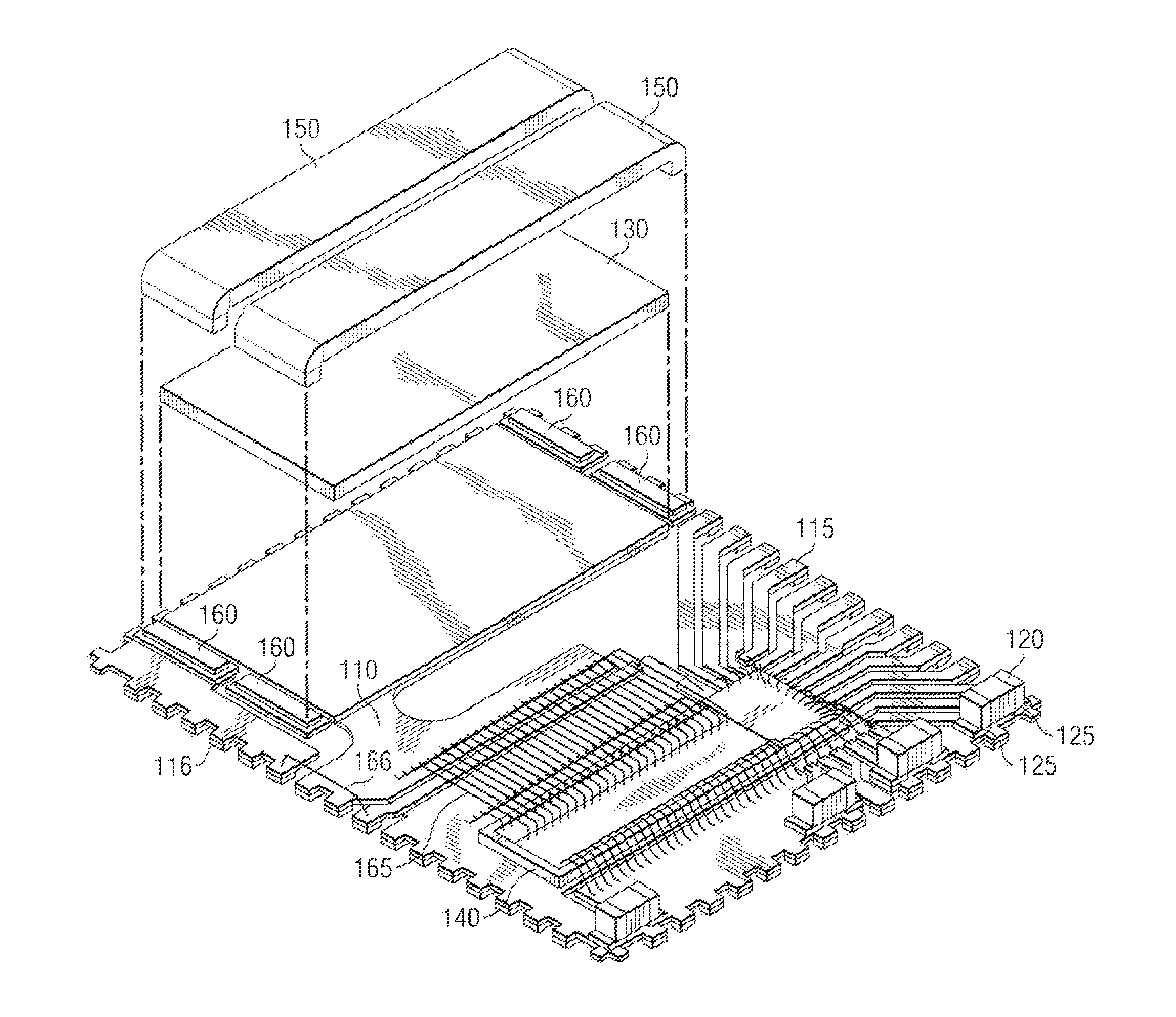
Referring initially to FIGS. 1 and 2, illustrated are isometric views of an embodiment of an electronic device (e.g., power module), before encapsulation, constructed according to the principles of the present invention. The power module includes a magnetic device (e.g., inductor), an integrated circuit and surface-mount components. The power module may include power conversion circuitry that includes or may be embodied in the magnetic device, the integrated circuit and at least one of the surface-mount components. The power conversion circuitry may form a power converter that often includes switching regulators such as buck switching regulators with digital control circuits for reduced component count, and synchronous rectifiers for high power conversion efficiency. Of course, the broad scope of the present invention is not limited to a power module, power converter or the like, and may be applicable to other electronic devices.
A conductive substrate (e.g., conductive leadframe or leadframe) 110 is patterned and etched to form an electrically conductive interconnect layer for the lower portion of a winding for the inductor as well as the electrical interconnections among surface-mount components, the integrated circuit, and the inductor. A typical thickness of the leadframe 110 is about eight mils. While the leadframe 110 is often constructed of copper, alternative electrically conductive materials can be used therefor. The leadframe 110 provides external connections for the power module, as well as a support base for a magnetic material for the inductor. The external connections are formed as fingers of the leadframe 110, referenced as leadframe fingers (two of which are designated 115, 116).
The leadframe 110 is generally constructed with an integral strip surrounding the electrically conductive pattern to provide mechanical support during the manufacturing steps, which strip is discarded later in the manufacturing process. The surrounding strip is generally sheared off after the electronic device has been constructed. The leadframe 110 is generally produced in an array of repeating of patterns (not shown), such as a 16.times.16 array, to form, for example, 256 substantially identical electronic devices. Forming an array of leadframes 110 is a process well known in the art to reduce the manufacturing cost of producing the electronic devices.
Solder paste is selectively applied to the leadframe 110 in a thin layer to areas (one of which is designated 125) for screening processes, to provide electrical and mechanical attachment for surface-mount components. The surface-mount components such as capacitors (one of which is designated 120) are placed with their conductive ends in the solder paste. The solder paste may be composed of lead-based as well as lead-free compositions. The array of leadframes 110 with the surface-mount components 120 is reflowed in an oven to mechanically and electrically attach the surface-mount components 120 to the leadframe 110.
The steps as described above generally do not require execution in the highly controlled environment of a clean room. The following steps, however, are preferably performed in a clean room environment such as typically used for assembly of integrated circuits into a molded plastic package, as is generally well known in the art.
An adhesive (e.g., a die attach adhesive such as Abletherm 2600AT by Ablestik of Rancho Dominguez, Calif.) is dispensed onto the leadframe 110 to hold a magnetic core (e.g., a bar of magnetic material) 130 and an integrated circuit in the form of a semiconductor die 140. The bar of magnetic material 130 and the semiconductor die 140 are positioned on the leadframe 110 over the die attach adhesive. Thus, a lower surface of the bar of magnetic material 130 faces, and is preferably adhered to, the leadframe 110. The bar of magnetic material 130 is included to enhance the magnetic properties of the inductor and may be about 250 micrometers (.mu.m) thick, four mils wide and 7.5 mils long. The adhesive is cured, typically in a controlled thermal process, to secure the bar of magnetic material 130 and the semiconductor die 140 to the leadframe 110.
Solder paste is applied to areas (generally designated 160) of the leadframe 110 wherein ends of conductive clips 150 are placed. Again, the solder paste may be composed of lead-based as well as lead-free compositions. The conductive clips 150 (e.g., about 8-12 mils thick) are placed on the leadframe 110 above the bars of magnetic material 130 with their ends in the solder paste. The conductive clips 150 are formed with their ends bent toward the leadframe 110 about ends of the bar of magnetic material 130 without mechanical interference. Thus, an upper surface of the bar of magnetic material 130 faces the conductive clips 150. An insulating gap, for example, about a five mil air gap, is thus preferably left between the upper surfaces of the bars of magnetic material 130 and the lower surfaces of the conductive clips 150, which gap may be filled later by an encapsulant. The conductive clips 150 provide the portion of the electrically conductive inductor winding above each bar of magnetic material 130. The leadframe 110 is heated in a reflow oven to mechanically and electrically bond the conductive clips 150 to the leadframe 110.
Wire bonds preferably formed of gold wire such as a first wire bond 165 are attached to each semiconductor die 140 and to the leadframe 110 to electrically couple pads on the semiconductor die 140 to bonding areas of the leadframe 110 thereby providing electrical circuit connections therebetween. Wire bonds such as a second wire bond 166 may also be used to selectively electrically couple portions of the leadframe 110 to provide circuit interconnections that cannot be easily wired in a single planar layout, thus producing the topological layout equivalent for the leadframe 110 of a two-layer printed wiring board or substrate.
When the electronic devices are formed in an array as mentioned above, the array is placed in a mold, and an encapsulant such as a molding material, preferably epoxy, is deposited (e.g., injected) thereover as is well known in the art to provide environmental and mechanical protection as well as a thermally conductive covering to facilitate heat dissipation during operation. Other molding materials and processes as well as electronic devices constructed without an encapsulant are well within the broad scope of the present invention.
The individual electronic devices are singulated from the array thereof by a punching and shearing operation to produce an encapsulated power module including power conversion circuitry as illustrated with respect to FIG. 3. The power module is mechanically and hermetically protected by the encapsulant 170 as illustrated. External electrical connections to a system employing the power module are made via terminals 180 which are created from exposed leadframe fingers (see FIG. 1) protruding from sides and a lower surface of the power module after encapsulation. Typically, the terminals 180 are substantially coplanar with the sides and lower surface of the power module. The terminals 180 are formed by the shearing and molding operation on the leadframe 110 as is well known in the art.
Electrical connections to the system employing the power module are made by placing the power module on another circuit board or printed wiring board formed with interconnect pads that are covered with solder paste, generally by a screening operation, and heating the power module on the circuit board in a reflow oven. The reflow soldering operation is generally also adequate to provide mechanical attachment of the power module to another printed wiring board, but other attachment methods such as adhesive compound are well within the broad scope of the present invention.
Turning now to FIG. 4, illustrated is a diagram of an embodiment of a power converter including power conversion circuitry constructed according to the principles of the present invention. The power converter includes a power train 410, a controller 420 and a driver 430, and provides power to a system such as a microprocessor. While in the illustrated embodiment, the power train 410 employs a buck converter topology, those skilled in the art should understand that other converter topologies such as a forward converter topology are well within the broad scope of the present invention.
The power train 410 receives an input voltage V.sub.in from a source of electrical power (represented by a battery) at an input thereof and provides a regulated output voltage V.sub.out to power, for instance, a microprocessor at an output thereof. In keeping with the principles of a buck converter topology, the output voltage V.sub.out is generally less than the input voltage V.sub.in such that a switching operation of the power converter can regulate the output voltage V.sub.out. A switch (e.g., a main switch Q.sub.mn) is enabled to conduct for a primary interval (generally co-existent with a primary duty cycle "D" of the main switch Q.sub.mn) and couples the input voltage V.sub.in to an output filter inductor L.sub.out. During the primary interval, an inductor current L.sub.out flowing through the output filter inductor L.sub.out increases as a current flows from the input to the output of the power train 410. A component of the inductor current I.sub.Lout is filtered by the output capacitor C.sub.out.
During a complementary interval (generally co-existent with a complementary duty cycle "1-D" of the main switch Q.sub.mn), the main switch Q.sub.mn is transitioned to a non-conducting state and another switch (e.g., an auxiliary switch Q.sub.aux) is enabled to conduct. The auxiliary switch Q.sub.aux provides a path to maintain a continuity of the inductor current I.sub.Lout flowing through the output filter inductor L.sub.out. During the complementary interval, the inductor current I.sub.Lout through the output filter inductor L.sub.out decreases. In general, the duty cycle of the main and auxiliary switches Q.sub.mn, Q.sub.aux may be adjusted to maintain a regulation of the output voltage V.sub.out of the power converter. Those skilled in the art should understand, however, that the conduction periods for the main and auxiliary switches Q.sub.mn, Q.sub.aux may be separated by a small time interval to avoid cross conduction therebetween and beneficially to reduce the switching losses associated with the power converter.
The controller 420 receives a desired characteristic such as a desired system voltage V.sub.system from an internal or external source associated with the microprocessor, and the output voltage V.sub.out of the power converter. The controller 420 is also coupled to the input voltage V.sub.in of the power converter and a return lead of the source of electrical power (again, represented by a battery) to provide a ground connection therefor. A decoupling capacitor C.sub.dec is coupled to the path from the input voltage V.sub.in to the controller 420. The decoupling capacitor C.sub.dec is configured to absorb high frequency noise signals associated with the source of electrical power to protect the controller 420.
In accordance with the aforementioned characteristics, the controller 420 provides a signal (e.g., a pulse width modulated signal S.sub.PWM) to control a duty cycle and a frequency of the main and auxiliary switches Q.sub.mn, Q.sub.aux of the power train 410 to regulate the output voltage V.sub.out thereof. The controller 420 may also provide a complement of the signal (e.g., a complementary pulse width modulated signal S.sub.1-PWM) in accordance with the aforementioned characteristics. Any controller adapted to control at least one switch of the power converter is well within the broad scope of the present invention. As an example, a controller employing digital circuitry is disclosed in U.S. Patent Application Publication No. 2005/0169024, entitled "Controller for a Power Converter and a Method of Controlling a Switch Thereof," to Dwarakanath, et al. and U.S. Patent Application Publication No. 2005/0168205, entitled "Controller for a Power Converter and Method of Controlling a Switch Thereof," to Dwarakanath, et al., which are incorporated herein by reference.
The power converter also includes the driver 430 configured to provide drive signals S.sub.DRV1, S.sub.DRV2 to the main and auxiliary switches Q.sub.mn, Q.sub.aux, respectively, based on the signals S.sub.PWM, S.sub.1-PWM provided by the controller 420. There are a number of viable alternatives to implement a driver 430 that include techniques to provide sufficient signal delays to prevent crosscurrents when controlling multiple switches in the power converter. The driver 430 typically includes switching circuitry incorporating a plurality of driver switches that cooperate to provide the drive signals S.sub.DRV1, S.sub.DRV2 to the main and auxiliary switches Q.sub.mn, Q.sub.aux. Of course, any driver 430 capable of providing the drive signals S.sub.DRV1, S.sub.DRV2 to control a switch is well within the broad scope of the present invention. As an example, a driver is disclosed in U.S. Patent Application Publication No. 2005/0168203, entitled "Driver for a Power Converter and Method of Driving a Switch Thereof," to Dwarakanath, et al., which is incorporated herein by reference. Also, an embodiment of a semiconductor device that may embody portions of the power conversion circuitry is disclosed in U.S. Patent Application Publication No. 2005/0167756, entitled "Laterally Diffused Metal Oxide Semiconductor Device and Method of Forming the Same," to Lotfi, et al., which is incorporated herein by reference, and an embodiment of an integrated circuit embodying power conversion circuitry, or portions thereof, is disclosed in U.S. Patent Application Publication No. 2006/0038225, entitled "Integrated Circuit Employable with a Power Converter," to Lotfi, et al., which is incorporated by reference.
Thus, a magnetic device, a power module and a method of manufacture thereof with readily attainable and quantifiable advantages have been introduced. Those skilled in the art should understand that the previously described embodiments of the magnetic device and power module are submitted for illustrative purposes only. In addition, other embodiments capable of producing a magnetic device and a power module while addressing compact, efficient and high density power modules, while being manufacturable at high volume and with lower cost than is achieved with the prior art are well within the broad scope of the present invention. While the magnetic device has been described in the environment of a power converter, the magnetic device may also be incorporated into other electronic devices, systems or assemblies such as communication or computing devices or other power processing devices.
As mentioned above, the present invention provides a magnetic device including a magnetic core having a surface facing a conductive substrate and a conductive clip facing a surface of the magnetic core with ends of the conductive clip electrically coupled to the conductive substrate to cooperatively form a winding therewith about the magnetic core. As an example, the present invention provides an inductor compatible with ordinary manufacturing and packaging processes for power management integrated circuits. The inductor includes a magnetic core formed from a bar of magnetic material adhered to conductive substrate (e.g., a patterned, conductive leadframe) and at least one conductive clip is placed above the bar of magnetic material to complete the portion of the inductor winding above the leadframe. Preferably, the conductive clip is made of copper, but other electrically conductive materials are well within the broad scope of the present invention. The bar of magnetic material is adhered to the leadframe with a die attach adhesive, and the at least one conductive clip is soldered to the leadframe. The inductor is preferably encapsulated with plastic encapsulating compound including an epoxy.
In an exemplary embodiment, the bar of magnetic material includes a ceramic material such as a soft magnetic ferrite having manganese zinc or nickel zinc ferrite. In a further exemplary embodiment, the bar of magnetic material is formed with a metallic alloy such as an iron cobalt alloy deposited via an electroplating process on a semiconductor or insulating die such as a silicon die. The at least one conductive clip may be soldered to the leadframe in a reflow soldering process. Additionally, a gap may be formed between the at least one conductive clip and the bar of magnetic material. In accordance therewith, the gap is typically filled with plastic encapsulating compound. The integrated circuit is also adhered to the leadframe. Preferably, the integrated circuit is wire bonded (via, for instance, gold wires) to the leadframe to form electrical connections therebetween. Surface-mount components may also be soldered to the leadframe.
In accordance with another aspect of the present invention, a magnetic device, integrated circuit and surface-mount components are integrated to form an electronic device such as a power module or power management integrated circuit. In other aspects, the present invention provides methods of forming the magnetic device and power module that take advantage of current practices in the field of power management integrated circuits.
For a better understanding of power converters, see "Modern DC-to-DC Switchmode Power Converter Circuits," by Rudolph P. Severns and Gordon Bloom, Van Nostrand Reinhold Company, New York, N.Y. (1985) and "Principles of Power Electronics," by J. G. Kassakian, M. F. Schlecht and G. C. Verghese, Addison-Wesley (1991). For a better understanding of magnetic devices, see "Soft Ferrites: Properties and Applications," by E. C. Snelling, published by Butterworth-Heinemann, Second Edition, 1989. The aforementioned references are incorporated herein by reference in their entirety.
Also, although the present invention and its advantages have been described in detail, it should be understood that various changes, substitutions and alterations can be made herein without departing from the spirit and scope of the invention as defined by the appended claims. For example, many of the processes discussed above can be implemented in different methodologies and replaced by other processes, or a combination thereof.
Moreover, the scope of the present application is not intended to be limited to the particular embodiments of the process, machine, manufacture, composition of matter, means, methods and steps described in the specification. As one of ordinary skill in the art will readily appreciate from the disclosure of the present invention, processes, machines, manufacture, compositions of matter, means, methods, or steps, presently existing or later to be developed, that perform substantially the same function or achieve substantially the same result as the corresponding embodiments described herein may be utilized according to the present invention. Accordingly, the appended claims are intended to include within their scope such processes, machines, manufacture, compositions of matter, means, methods, or steps.
* * * * *
D00000
D00001
D00002
D00003
XML
uspto.report is an independent third-party trademark research tool that is not affiliated, endorsed, or sponsored by the United States Patent and Trademark Office (USPTO) or any other governmental organization. The information provided by uspto.report is based on publicly available data at the time of writing and is intended for informational purposes only.
While we strive to provide accurate and up-to-date information, we do not guarantee the accuracy, completeness, reliability, or suitability of the information displayed on this site. The use of this site is at your own risk. Any reliance you place on such information is therefore strictly at your own risk.
All official trademark data, including owner information, should be verified by visiting the official USPTO website at www.uspto.gov. This site is not intended to replace professional legal advice and should not be used as a substitute for consulting with a legal professional who is knowledgeable about trademark law.