Discrete flexible interconnects for modules of integrated circuits
Dalal , et al.
U.S. patent number 10,297,572 [Application Number 14/870,802] was granted by the patent office on 2019-05-21 for discrete flexible interconnects for modules of integrated circuits. This patent grant is currently assigned to MC10, INC.. The grantee listed for this patent is MC10, Inc.. Invention is credited to Mitul Dalal, Sanjay Gupta.
| United States Patent | 10,297,572 |
| Dalal , et al. | May 21, 2019 |
Discrete flexible interconnects for modules of integrated circuits
Abstract
Flexible interconnects, flexible integrated circuit systems and devices, and methods of making and using flexible integrated circuitry are presented herein. A flexible integrated circuit system is disclosed which includes first and second discrete devices that are electrically connected by a discrete flexible interconnect. The first discrete devices includes a first flexible multi-layer integrated circuit (IC) package with a first electrical connection pad on an outer surface thereof. The second discrete device includes a second flexible multi-layer integrated circuit (IC) package with a second electrical connection pad on an outer surface thereof. The discrete flexible interconnect is attached to and electrically connects the first electrical connection pad of the first discrete device to the second electrical connection pad of the second discrete device.
| Inventors: | Dalal; Mitul (South Grafton, MA), Gupta; Sanjay (Bedford, MA) | ||||||||||
|---|---|---|---|---|---|---|---|---|---|---|---|
| Applicant: |
|
||||||||||
| Assignee: | MC10, INC. (Lexington,
MA) |
||||||||||
| Family ID: | 55633335 | ||||||||||
| Appl. No.: | 14/870,802 | ||||||||||
| Filed: | September 30, 2015 |
Prior Publication Data
| Document Identifier | Publication Date | |
|---|---|---|
| US 20160099227 A1 | Apr 7, 2016 | |
Related U.S. Patent Documents
| Application Number | Filing Date | Patent Number | Issue Date | ||
|---|---|---|---|---|---|
| 62060147 | Oct 6, 2014 | ||||
| Current U.S. Class: | 1/1 |
| Current CPC Class: | H01L 24/19 (20130101); H01L 24/20 (20130101); H01L 24/73 (20130101); H01L 24/48 (20130101); H01L 25/0655 (20130101); H01L 24/95 (20130101); H01L 23/66 (20130101); H01L 24/50 (20130101); H01L 24/92 (20130101); H01L 25/50 (20130101); H01L 23/5385 (20130101); H01L 24/32 (20130101); H01L 23/5383 (20130101); H01L 23/5389 (20130101); H01L 23/5387 (20130101); H01L 2224/73265 (20130101); H01L 2224/85203 (20130101); H01L 2224/73267 (20130101); H01L 2224/50 (20130101); H01L 2224/85005 (20130101); H01L 2224/73219 (20130101); H01L 2224/85801 (20130101); H01L 2224/04042 (20130101); H01L 2224/32225 (20130101); H01L 2224/45144 (20130101); H01L 2224/85205 (20130101); H01L 2224/85207 (20130101); H01L 2924/00014 (20130101); H01L 24/45 (20130101); H01L 24/83 (20130101); H05K 1/147 (20130101); H01L 2224/05553 (20130101); H01L 2224/4809 (20130101); H01L 2224/8385 (20130101); H01L 2224/92247 (20130101); H01L 2223/6616 (20130101); H05K 1/0298 (20130101); H01L 2224/86005 (20130101); H01L 2224/48157 (20130101); H01L 24/13 (20130101); H01L 24/85 (20130101); H01L 2224/05554 (20130101); H01L 2224/131 (20130101); H01L 2224/45015 (20130101); H01L 2224/16227 (20130101); H01L 2924/14 (20130101); H01L 25/105 (20130101); H01L 24/16 (20130101); H01L 2224/92248 (20130101); H01L 2224/95 (20130101); H01L 2224/04105 (20130101); H01L 2224/92244 (20130101); H01L 2224/49176 (20130101); H01L 24/86 (20130101); H01L 2224/32013 (20130101); H01L 2224/48101 (20130101); H01L 2224/45147 (20130101); H05K 1/189 (20130101); H01L 2223/6677 (20130101); H01L 24/49 (20130101); H01L 2224/86801 (20130101); H01L 2224/2919 (20130101); H01L 24/29 (20130101); H01L 2224/95001 (20130101); H01L 2224/48091 (20130101); H01L 2224/48499 (20130101); H01L 2224/45144 (20130101); H01L 2924/00014 (20130101); H01L 2224/45147 (20130101); H01L 2924/00014 (20130101); H01L 2224/85203 (20130101); H01L 2924/00014 (20130101); H01L 2224/85205 (20130101); H01L 2924/00014 (20130101); H01L 2224/85207 (20130101); H01L 2924/00014 (20130101); H01L 2224/45015 (20130101); H01L 2924/00014 (20130101); H01L 2224/48091 (20130101); H01L 2924/00014 (20130101); H01L 2224/4809 (20130101); H01L 2924/00012 (20130101); H01L 2224/48499 (20130101); H01L 2924/014 (20130101); H01L 2224/85801 (20130101); H01L 2924/00014 (20130101); H01L 2224/131 (20130101); H01L 2924/014 (20130101); H01L 2224/95 (20130101); H01L 2224/19 (20130101); H01L 2224/95 (20130101); H01L 2224/85 (20130101); H01L 2224/95 (20130101); H01L 2224/86 (20130101); H01L 2224/86801 (20130101); H01L 2924/00014 (20130101); H01L 2224/8385 (20130101); H01L 2924/00014 (20130101); H01L 2224/2919 (20130101); H01L 2924/00014 (20130101); H01L 2924/00014 (20130101); H01L 2224/05599 (20130101); H01L 2924/00014 (20130101); H01L 2224/85399 (20130101) |
| Current International Class: | H01L 25/00 (20060101); H01L 23/66 (20060101); H01L 23/00 (20060101); H01L 25/065 (20060101); H01L 23/538 (20060101) |
References Cited [Referenced By]
U.S. Patent Documents
| 3716861 | February 1973 | Root |
| 3805427 | April 1974 | Epstein |
| 4304235 | December 1981 | Kaufman |
| 4416288 | November 1983 | Freeman |
| 4558395 | December 1985 | Yamada |
| 4658153 | April 1987 | Brosh |
| 5050036 | September 1991 | Oudick |
| 5306917 | April 1994 | Black |
| 5326521 | July 1994 | East |
| 5331966 | July 1994 | Bennett |
| 5360987 | November 1994 | Shibib |
| 5454270 | October 1995 | Brown |
| 5491651 | February 1996 | Janic |
| 5567975 | October 1996 | Walsh |
| 5580794 | December 1996 | Allen |
| 5617870 | April 1997 | Hastings |
| 5776797 | July 1998 | Nicewarner, Jr. |
| 5811790 | September 1998 | Endo |
| 5817008 | October 1998 | Rafert |
| 5907477 | May 1999 | Tuttle |
| 6027958 | February 2000 | Vu |
| 6063046 | May 2000 | Allum |
| 6265090 | July 2001 | Nishide |
| 6282960 | September 2001 | Samuels et al. |
| 6343514 | February 2002 | Smith |
| 6387052 | May 2002 | Quinn |
| 6421016 | July 2002 | Phillips |
| 6455930 | September 2002 | Palanisamy |
| 6455931 | September 2002 | Hamilton |
| 6567158 | May 2003 | Falcial |
| 6641860 | November 2003 | Kaiserman |
| 6775906 | August 2004 | Silverbrook |
| 6784844 | August 2004 | Boakes |
| 6936855 | August 2005 | Harrah |
| 6965160 | November 2005 | Cobbley |
| 6987314 | January 2006 | Yoshida |
| 7141874 | November 2006 | Nakatani |
| 7259030 | August 2007 | Daniels |
| 7265298 | September 2007 | Maghribi |
| 7302751 | December 2007 | Hamburgen |
| 7337012 | February 2008 | Maghribi |
| 7487587 | February 2009 | Vanfleteren |
| 7491892 | February 2009 | Wagner |
| 7521292 | April 2009 | Rogers |
| 7557367 | July 2009 | Rogers |
| 7618260 | November 2009 | Daniel |
| 7622367 | November 2009 | Nuzzo |
| 7649245 | January 2010 | Zingher |
| 7656673 | February 2010 | Fries |
| 7727228 | June 2010 | Abboud |
| 7739791 | June 2010 | Brandenburg |
| 7759167 | July 2010 | Vanfleteren |
| 7960246 | June 2011 | Flamand |
| 7982296 | July 2011 | Nuzzo |
| 8097926 | January 2012 | De Graff |
| 8129823 | March 2012 | Tanikella |
| 8198621 | June 2012 | Rogers |
| 8207473 | June 2012 | Axisa |
| 8217381 | July 2012 | Rogers |
| 8372726 | February 2013 | De Graff |
| 8389862 | March 2013 | Arora |
| 8431828 | April 2013 | Vanfleteren |
| 8440546 | May 2013 | Nuzzo |
| 8472207 | June 2013 | Rendek, Jr. |
| 8536667 | September 2013 | De Graff |
| 8552299 | October 2013 | Rogers |
| 8664699 | March 2014 | Nuzzo |
| 8679888 | March 2014 | Rogers |
| 8729524 | May 2014 | Rogers |
| 8754396 | June 2014 | Rogers |
| 8865489 | October 2014 | Rogers |
| 8879276 | November 2014 | Wang |
| 8886334 | November 2014 | Ghaffari |
| 8905772 | December 2014 | Rogers |
| 9012784 | April 2015 | Arora |
| 9082025 | July 2015 | Fastert |
| 9105555 | August 2015 | Rogers |
| 9105782 | August 2015 | Rogers |
| 9119533 | September 2015 | Ghaffari |
| 9123614 | September 2015 | Graff |
| 9159635 | October 2015 | Elolampi |
| 9168094 | October 2015 | Lee |
| 9171794 | October 2015 | Rafferty |
| 9186060 | November 2015 | De Graff |
| 9209151 | December 2015 | Chauhan |
| 9407798 | August 2016 | Havskjold |
| 2001/0006252 | July 2001 | Kim |
| 2001/0012918 | August 2001 | Swanson |
| 2001/0021867 | September 2001 | Kordis |
| 2002/0026127 | February 2002 | Balbierz |
| 2002/0082515 | June 2002 | Campbell |
| 2002/0094701 | July 2002 | Biegelsen |
| 2002/0113739 | August 2002 | Howard |
| 2002/0128700 | September 2002 | Cross, Jr. |
| 2002/0145467 | October 2002 | Minch |
| 2002/0151934 | October 2002 | Levine |
| 2002/0158330 | October 2002 | Moon |
| 2003/0017848 | January 2003 | Engstrom |
| 2003/0045025 | March 2003 | Coyle |
| 2003/0081392 | May 2003 | Cady |
| 2003/0097165 | May 2003 | Krulevitch |
| 2003/0120271 | June 2003 | Burnside |
| 2003/0162507 | August 2003 | Vatt |
| 2003/0214408 | November 2003 | Grajales |
| 2003/0236455 | December 2003 | Swanson |
| 2004/0006264 | January 2004 | Mojarradi |
| 2004/0052052 | March 2004 | Rivera |
| 2004/0085469 | May 2004 | Johnson |
| 2004/0092806 | May 2004 | Sagon |
| 2004/0106334 | June 2004 | Suzuki |
| 2004/0135094 | July 2004 | Niigaki |
| 2004/0138558 | July 2004 | Dunki-Jacobs |
| 2004/0149921 | August 2004 | Smyk |
| 2004/0178466 | September 2004 | Merrill |
| 2004/0192082 | September 2004 | Wagner |
| 2004/0201134 | October 2004 | Kawai |
| 2004/0203486 | October 2004 | Shepherd |
| 2004/0221370 | November 2004 | Hannula |
| 2004/0243204 | December 2004 | Maghribi |
| 2005/0021103 | January 2005 | DiLorenzo |
| 2005/0067293 | March 2005 | Naito |
| 2005/0070778 | March 2005 | Lackey |
| 2005/0096513 | May 2005 | Ozguz |
| 2005/0113744 | May 2005 | Donoghue |
| 2005/0139683 | June 2005 | Yi |
| 2005/0171524 | August 2005 | Stern |
| 2005/0203366 | September 2005 | Donoghue |
| 2006/0003709 | January 2006 | Wood |
| 2006/0038182 | February 2006 | Rogers |
| 2006/0071349 | April 2006 | Tokushige |
| 2006/0084394 | April 2006 | Engstrom |
| 2006/0106321 | May 2006 | Lewinsky |
| 2006/0128346 | June 2006 | Yasui |
| 2006/0154398 | July 2006 | Qing |
| 2006/0160560 | July 2006 | Josenhans |
| 2006/0248946 | November 2006 | Howell |
| 2006/0257945 | November 2006 | Masters |
| 2006/0264767 | November 2006 | Shennib |
| 2006/0286785 | December 2006 | Rogers |
| 2007/0027514 | February 2007 | Gerber |
| 2007/0031283 | February 2007 | Davis |
| 2007/0108389 | May 2007 | Makela |
| 2007/0113399 | May 2007 | Kumar |
| 2007/0123756 | May 2007 | Kitajima |
| 2007/0270672 | November 2007 | Hayter |
| 2008/0046080 | February 2008 | Vanden Bulcke |
| 2008/0074383 | March 2008 | Dean |
| 2008/0096620 | April 2008 | Lee |
| 2008/0139894 | June 2008 | Szydlo-Moore |
| 2008/0143379 | June 2008 | Norman |
| 2008/0157235 | July 2008 | Rogers |
| 2008/0193749 | August 2008 | Thompson |
| 2008/0204021 | August 2008 | Leussler |
| 2008/0211087 | September 2008 | Mueller-Hipper |
| 2008/0237840 | October 2008 | Alcoe |
| 2008/0259576 | October 2008 | Johnson |
| 2008/0287167 | November 2008 | Caine |
| 2008/0313552 | December 2008 | Buehler |
| 2009/0000377 | January 2009 | Shipps |
| 2009/0001550 | January 2009 | Li |
| 2009/0015560 | January 2009 | Robinson |
| 2009/0016032 | January 2009 | Chow |
| 2009/0017884 | January 2009 | Rotschild |
| 2009/0048556 | February 2009 | Durand |
| 2009/0088750 | April 2009 | Hushka |
| 2009/0107704 | April 2009 | Vanfleteren |
| 2009/0154736 | June 2009 | Lee |
| 2009/0184254 | July 2009 | Miura |
| 2009/0204168 | August 2009 | Kallmyer |
| 2009/0215385 | August 2009 | Waters |
| 2009/0225751 | September 2009 | Koenck |
| 2009/0261828 | October 2009 | Nordmeyer-Massner |
| 2009/0273909 | November 2009 | Shin |
| 2009/0283891 | November 2009 | Dekker |
| 2009/0291508 | November 2009 | Babu |
| 2009/0294803 | December 2009 | Nuzzo |
| 2009/0302760 | December 2009 | Tchakarov |
| 2009/0322480 | December 2009 | Benedict |
| 2010/0002402 | January 2010 | Rogers |
| 2010/0059863 | March 2010 | Rogers |
| 2010/0072577 | March 2010 | Nuzzo |
| 2010/0073669 | March 2010 | Colvin |
| 2010/0087782 | April 2010 | Ghaffari |
| 2010/0090781 | April 2010 | Yamamoto |
| 2010/0090824 | April 2010 | Rowell |
| 2010/0116526 | May 2010 | Arora |
| 2010/0117660 | May 2010 | Douglas |
| 2010/0178722 | July 2010 | De Graff |
| 2010/0245011 | September 2010 | Chatzopoulos |
| 2010/0271191 | October 2010 | De Graff |
| 2010/0298895 | November 2010 | Ghaffari |
| 2010/0317132 | December 2010 | Rogers |
| 2010/0321161 | December 2010 | Isabell |
| 2010/0327387 | December 2010 | Kasai |
| 2011/0011179 | January 2011 | Gustafsson |
| 2011/0034912 | February 2011 | De Graff |
| 2011/0051384 | March 2011 | Kriechbaum |
| 2011/0054583 | March 2011 | Litt |
| 2011/0101789 | May 2011 | Salter |
| 2011/0121822 | May 2011 | Parsche |
| 2011/0140897 | June 2011 | Purks |
| 2011/0175735 | July 2011 | Forster |
| 2011/0184320 | July 2011 | Shipps |
| 2011/0215931 | September 2011 | Callsen |
| 2011/0218756 | September 2011 | Callsen |
| 2011/0218757 | September 2011 | Callsen |
| 2011/0220890 | September 2011 | Nuzzo |
| 2011/0277813 | November 2011 | Rogers |
| 2011/0306851 | December 2011 | Wang |
| 2012/0016258 | January 2012 | Webster |
| 2012/0051005 | March 2012 | Vanfleteren |
| 2012/0052268 | March 2012 | Axisa |
| 2012/0065937 | March 2012 | De Graff |
| 2012/0074546 | March 2012 | Chong |
| 2012/0087216 | April 2012 | Keung |
| 2012/0091594 | April 2012 | Landesberger |
| 2012/0092178 | April 2012 | Callsen |
| 2012/0092222 | April 2012 | Kato |
| 2012/0101413 | April 2012 | Beetel |
| 2012/0101538 | April 2012 | Ballakur |
| 2012/0108012 | May 2012 | Yasuda |
| 2012/0157804 | June 2012 | Rogers |
| 2012/0170231 | July 2012 | Lee |
| 2012/0172697 | July 2012 | Urman |
| 2012/0226130 | September 2012 | De Graff |
| 2012/0244848 | September 2012 | Ghaffari |
| 2012/0256308 | October 2012 | Helin |
| 2012/0314382 | December 2012 | Wesselmann |
| 2012/0316455 | December 2012 | Rahman |
| 2012/0327608 | December 2012 | Rogers |
| 2013/0041235 | February 2013 | Rogers |
| 2013/0056862 | March 2013 | Kim |
| 2013/0099358 | April 2013 | Elolampi |
| 2013/0100618 | April 2013 | Rogers |
| 2013/0118255 | May 2013 | Callsen |
| 2013/0150693 | June 2013 | D'angelo |
| 2013/0185003 | July 2013 | Carbeck |
| 2013/0192356 | August 2013 | De Graff |
| 2013/0200268 | August 2013 | Rafferty |
| 2013/0211761 | August 2013 | Brandsma |
| 2013/0214300 | August 2013 | Lerman |
| 2013/0215467 | August 2013 | Fein |
| 2013/0225965 | August 2013 | Ghaffari |
| 2013/0237150 | September 2013 | Royston |
| 2013/0245388 | September 2013 | Rafferty |
| 2013/0274562 | October 2013 | Ghaffari |
| 2013/0313713 | November 2013 | Arora |
| 2013/0316442 | November 2013 | Meurville |
| 2013/0316487 | November 2013 | De Graff |
| 2013/0320503 | December 2013 | Nuzzo |
| 2013/0321373 | December 2013 | Yoshizumi |
| 2013/0335011 | December 2013 | Bohringer |
| 2014/0001058 | January 2014 | Ghaffari |
| 2014/0012160 | January 2014 | Ghaffari |
| 2014/0012242 | January 2014 | Lee |
| 2014/0021522 | January 2014 | Lin |
| 2014/0022746 | January 2014 | Hsu |
| 2014/0039290 | February 2014 | De Graff |
| 2014/0097944 | April 2014 | Fastert |
| 2014/0110859 | April 2014 | Rafferty |
| 2014/0133179 | May 2014 | Franklin |
| 2014/0140020 | May 2014 | Rogers |
| 2014/0183698 | July 2014 | Hsu |
| 2014/0188426 | July 2014 | Fastert |
| 2014/0191236 | July 2014 | Nuzzo |
| 2014/0216524 | August 2014 | Rogers |
| 2014/0240932 | August 2014 | Hsu |
| 2014/0249520 | September 2014 | Ghaffari |
| 2014/0268594 | September 2014 | Wang |
| 2014/0268780 | September 2014 | Wang |
| 2014/0303452 | October 2014 | Ghaffari |
| 2014/0340857 | November 2014 | Hsu |
| 2014/0364794 | December 2014 | Jordan |
| 2014/0374872 | December 2014 | Rogers |
| 2014/0375465 | December 2014 | Fenuccio |
| 2015/0001462 | January 2015 | Rogers |
| 2015/0019135 | January 2015 | Kacyvenski |
| 2015/0035680 | February 2015 | Li |
| 2015/0069617 | March 2015 | Arora |
| 2015/0099976 | April 2015 | Ghaffari |
| 2015/0100135 | April 2015 | Ives |
| 2015/0194817 | July 2015 | Lee |
| 2015/0237711 | August 2015 | Rogers |
| 2015/0241288 | August 2015 | Keen |
| 2015/0260713 | September 2015 | Ghaffari |
| 2015/0272652 | October 2015 | Ghaffari |
| 2015/0286913 | October 2015 | Fastert |
| 2015/0320472 | November 2015 | Ghaffari |
| 2015/0335254 | November 2015 | Fastert |
| 2015/0342036 | November 2015 | Elolampi |
| 2015/0348942 | December 2015 | Kim |
| 2015/0380848 | December 2015 | Kato |
| 2016/0056102 | February 2016 | Konchady |
| 103619590 | Mar 2014 | CN | |||
| 0585670 | Mar 1994 | EP | |||
| 2259062 | Dec 2010 | EP | |||
| H04 290489 | Oct 1992 | JP | |||
| 05-087511 | Apr 1993 | JP | |||
| 2009-170173 | Jul 2009 | JP | |||
| WO 99/38211 | Jul 1999 | WO | |||
| WO 2005/122285 | Dec 2005 | WO | |||
| WO 03/021679 | Mar 2006 | WO | |||
| WO 2007/003019 | Jan 2007 | WO | |||
| WO 2007/116344 | Oct 2007 | WO | |||
| WO 2007/136726 | Nov 2007 | WO | |||
| WO 2008/030960 | Mar 2008 | WO | |||
| WO 2009/111641 | Sep 2009 | WO | |||
| WO 2009/114689 | Sep 2009 | WO | |||
| WO 2010/036807 | Apr 2010 | WO | |||
| WO 2010/042653 | Apr 2010 | WO | |||
| WO 2010/042957 | Apr 2010 | WO | |||
| WO 2010/046883 | Apr 2010 | WO | |||
| WO 2010/056857 | May 2010 | WO | |||
| WO 2010/081137 | Jul 2010 | WO | |||
| WO 2010/082993 | Jul 2010 | WO | |||
| WO 2010/102310 | Sep 2010 | WO | |||
| WO 2010/132552 | Nov 2010 | WO | |||
| WO 2011/003181 | Jan 2011 | WO | |||
| WO 2011/041727 | Apr 2011 | WO | |||
| WO 2011/084450 | Jul 2011 | WO | |||
| WO 2011/084709 | Jul 2011 | WO | |||
| WO 2011/127331 | Oct 2011 | WO | |||
| WO 2012/125494 | Sep 2012 | WO | |||
| WO 2012/166686 | Dec 2012 | WO | |||
| WO 2013/010171 | Jan 2013 | WO | |||
| WO 2013/022853 | Feb 2013 | WO | |||
| WO 2013/033724 | Mar 2013 | WO | |||
| WO 2013/034987 | Mar 2013 | WO | |||
| WO 2013/049716 | Apr 2013 | WO | |||
| WO 2013/052919 | Apr 2013 | WO | |||
| WO 2013/170032 | Nov 2013 | WO | |||
| WO 2014/007871 | Jan 2014 | WO | |||
| WO 2014/058473 | Apr 2014 | WO | |||
| WO 2014/059032 | Apr 2014 | WO | |||
| WO 2014/106041 | Jul 2014 | WO | |||
| WO 2014/110176 | Jul 2014 | WO | |||
| WO 2014/130928 | Aug 2014 | WO | |||
| WO 2014/130931 | Aug 2014 | WO | |||
| WO 2014/186467 | Nov 2014 | WO | |||
| WO 2014/197443 | Dec 2014 | WO | |||
| WO 2014/205434 | Dec 2014 | WO | |||
| WO 2015/021039 | Feb 2015 | WO | |||
| WO 2015/054312 | Apr 2015 | WO | |||
| WO 2015/077559 | May 2015 | WO | |||
| WO 2015/080991 | Jun 2015 | WO | |||
| WO 2015/102951 | Jul 2015 | WO | |||
| WO 2015/103483 | Jul 2015 | WO | |||
| WO 2015/103580 | Jul 2015 | WO | |||
| WO 2015/127458 | Aug 2015 | WO | |||
| WO 2015/134588 | Sep 2015 | WO | |||
| WO 2015/138712 | Sep 2015 | WO | |||
Other References
|
Carvalhal et al., "Electrochemical Detection in a Paper-Based Separation Device", Analytical Chemistry, vol. 82, No. 3, (1162-1165) (4 pages) (Jan. 7, 2010). cited by applicant . Demura et al., "Immobilization of Glucose Oxidase with Bombyx Mori Silk Fibroin by Only Stretching Treatment and its Application to Glucose Sensor," Biotechnology and Bioengineering, vol. 33, 598-603 (6 pages) (1989). cited by applicant . Ellerbee et al., "Quantifying Colorimetric Assays in Paper-Based Microfluidic Devices by Measuring the Transmission of Light through Paper," Analytical Chemistry, vol. 81, No. 20 8447-8452, (6 pages) (Oct. 15, 2009). cited by applicant . Halsted, "Ligature and Suture Material," Journal of the American Medical Association, vol. LX, No. 15, 1119-1126, (8 pages) (Apr. 12, 1913). cited by applicant . Kim et al., "Complementary Metal Oxide Silicon Integrated Circuits Incorporating Monolithically Integrated Stretchable Wavy Interconnects," Applied Physics Letters, vol. 93, 044102-044102.3 (3 pages) (Jul. 31, 2008). cited by applicant . Kim et al., "Dissolvable Films of Silk Fibroin for Ultrathin Conformal Bio-Integrated Electronics," Nature, 1-8 (8 pages) (Apr. 18, 2010). cited by applicant . Kim et al., "Materials and Noncoplanar Mesh Designs for Integrated Circuits with Linear Elastic Responses to Extreme Mechanical Deformations," PNAS, vol. 105, No. 48, 18675-18680 (6 pages) (Dec. 2, 2008). cited by applicant . Kim et al., "Stretchable and Foldable Silicon Integrated Circuits," Science, vol. 320, 507-511 (5 pages) (Apr. 25, 2008). cited by applicant . Kim et al., "Electrowetting on Paper for Electronic Paper Display," ACS Applied Materials & Interfaces, vol. 2, No. 11, (3318-3323) (6 pages) (Nov. 24, 2010). cited by applicant . Ko et al., "A Hemispherical Electronic Eye Camera Based on Compressible Silicon Optoelectronics," Nature, vol. 454, 748-753 (6 pages) (Aug. 7, 2008). cited by applicant . Lawrence et al., "Bioactive Silk Protein Biomaterial Systems for Optical Devices," Biomacromolecules, vol. 9, 1214-1220 (7 pages) (Nov. 4, 2008). cited by applicant . Meitl et al., "Transfer Printing by Kinetic Control of Adhesion to an Elastomeric Stamp," Nature, vol. 5, 33-38 (6 pages) (Jan. 2006). cited by applicant . Omenetto et al., "A New Route for Silk," Nature Photonics, vol. 2, 641-643 (3 pages) (Nov. 2008). cited by applicant . Omenetto et al., "New Opportunities for an Ancient Material," Science, vol. 329, 528-531 (5 pages) (Jul. 30, 2010). cited by applicant . Siegel et al., "Foldable Printed Circuit Boards on Paper Substrates," Advanced Functional Materials, vol. 20, No. 1, 28-35, (8 pages) (Jan. 8, 2010). cited by applicant . Tsukada et al., "Structural Changes of Silk Fibroin Membranes Induced by Immersion in Methanol Aqueous Solutions," Journal of Polymer Science, vol. 32, 961-968 (8 pages) (1994). cited by applicant . Wang et al., "Controlled Release From Multilayer Silk Biomaterial Coatings to Modulate Vascular Cell Responses" Biomaterials, 29, 894-903 (10 pages) (Nov. 28, 2008). cited by applicant . International Search Report, PCT/US2015/053647, 2 pages (Jan. 7, 2016). cited by applicant . Written Opinion, PCT/US2015/053647, 7 pages (Jan. 7, 2016). cited by applicant . Cauwe M. et al., "Flexible and Stretchable Circuit Technologies for Space Applications," 5.sup.th Electronic Materials, Processes and Packaging for Space, May 22, 2014, XP055449783, downloaded at https://escies.org/download/webDocumentFile?id=61963 (18 pages). cited by applicant . European Patent Office, Extended European Search Report in European Patent Application No. 15848328.9, dated Feb. 20, 2018 (10 pages). cited by applicant. |
Primary Examiner: Soward; Ida M
Attorney, Agent or Firm: Nixon Peabody LLP
Parent Case Text
CLAIM OF PRIORITY AND CROSS-REFERENCE TO RELATED APPLICATION
This application claims the benefit of priority to U.S. Provisional Patent Application No. 62/060,147, which was filed on Oct. 6, 2014, and is incorporated herein by reference in its entirety.
Claims
What is claimed:
1. A flexible integrated circuit system comprising: a first discrete device with a first flexible multi-layer integrated circuit (IC) package including a first outer surface with a first electrical connection pad, a first flexible polymeric substrate, a first microchip embedded in or on the first flexible polymeric substrate, a first adhesive layer on the first flexible polymeric substrate, and a first conductive layer coupled to the first adhesive layer; a second discrete device with a second flexible multi-layer integrated circuit (IC) package including a second outer surface with a second electrical connection pad, a second flexible polymeric substrate, a second microchip embedded in or on the second flexible polymeric substrate, a second adhesive layer on the second flexible polymeric substrate, and a second conductive layer coupled to the second adhesive layer; and a discrete flexible interconnect attached to and electrically connecting the first electrical connection pad of the first discrete device to the second electrical connection pad of the second discrete device.
2. The flexible integrated circuit system of claim 1, wherein the discrete flexible interconnect comprises one or more pliant metal wires.
3. The flexible integrated circuit system of claim 2, wherein the one or more pliant metal wires comprise in-plane loops or out-of-plane-loops, or both, configured to increase flexibility.
4. The flexible integrated circuit system of claim 1, wherein the discrete flexible interconnect comprises a pliant multi-layer semiconductor.
5. The flexible integrated circuit system of claim 4, wherein the first flexible multi-layer IC package, the second flexible multi-layer IC package, and the pliant multi-layer semiconductor of the discrete flexible interconnect all comprise common layers of materials.
6. The flexible integrated circuit system of claim 1, wherein the discrete flexible interconnect includes a conductive substrate fabricated from an electrically conductive paste.
7. The flexible integrated circuit system of claim 6, wherein the discrete flexible interconnect comprises a web of metallic interconnects printed onto the substrate.
8. The flexible integrated circuit system of claim 1, wherein the first flexible multi-layer IC package further comprises a first via extending through the first conductive layer and the first adhesive layer to the first microchip, and the second flexible multi-layer IC package further comprises a second via extending through the second conductive layer and the second adhesive layer to the second microchip.
9. The flexible integrated circuit system of claim 1, wherein the first flexible multi-layer IC package includes a first set of surface-mount-technology (SMT) components mounted on the first outer surface, and the second flexible multi-layer IC package includes a second set of SMT components mounted on the second outer surface.
10. The flexible integrated circuit system of claim 1, wherein the discrete flexible interconnect maintains substantially identical electrical conductivity when stretched up to approximately 100% or bent up to approximately 180 degrees, or both.
11. An extremely flexible integrated circuit apparatus comprising: a first flexible multi-layer integrated circuit (IC) package including: a first flexible polymeric substrate; a first microchip embedded in or on the first flexible polymeric substrate; a first pair of adhesive layers, each on a respective side of the first flexible polymeric substrate; a first pair of conductive sheets, each coupled to the first flexible polymeric substrate by a respective one of the first adhesive layers; and a first electrical connection pad attached or coupled to an outer surface of one of the first conductive sheets; a second flexible multi-layer integrated circuit (IC) package, which is separate and distinct from the first flexible multi-later IC package, including: a second flexible polymeric substrate; a second microchip embedded in or on the second flexible polymeric substrate; a second pair of adhesive layers, each on a respective side of the second flexible polymeric substrate; a second pair of conductive sheets, each coupled to the second flexible polymeric substrate by a respective one of the second adhesive layers; and a second electrical connection pad attached or coupled to an outer surface of one of the second conductive sheets; and a flexible interconnect separate and distinct from the first and second flexible multi-layer IC packages, the flexible interconnect electrically connecting the first electrical connection pad to the second electrical connection pad.
12. A method for assembling flexible integrated circuits, the method comprising: providing a first discrete device with a first flexible multi-layer integrated circuit (IC) package including a first outer surface with a first electrical connection pad, a first flexible polymeric substrate, a first microchip embedded in or on the first flexible polymeric substrate, a first adhesive layer on the first flexible polymeric substrate, and a first conductive sheet attached to the first flexible polymeric substrate by the first adhesive layer; providing a second discrete device with a second flexible multi-layer integrated circuit (IC) package including a second outer surface with a second electrical connection pad; and electrically connecting a discrete flexible interconnect to the first electrical connection pad of the first discrete device and the second electrical connection pad of the second discrete device.
13. The method of claim 12, wherein the discrete flexible interconnect comprises one or more pliant metal wires.
14. The method of claim 12, wherein the discrete flexible interconnect comprises a pliant multi-layer semiconductor.
15. The method of claim 12, wherein the discrete flexible interconnect includes a conductive substrate fabricated from an electrically conductive paste.
16. The method of claim 12, wherein the second flexible multi-layer IC package comprises a second flexible polymeric substrate, a second microchip embedded in or on the second flexible polymeric substrate, a second adhesive layer on the second flexible polymeric substrate, and a second conductive sheet attached to the second flexible polymeric substrate by the first adhesive layer.
Description
TECHNICAL FIELD
The present disclosure relates generally to printed circuit boards (PCB) and integrated circuits (IC). More particularly, aspects of this disclosure relate to bendable, stretchable and compressible interconnects for flexible integrated circuitry.
BACKGROUND
Integrated circuits (IC) are the cornerstone of the information age and the foundation of today's information technology industries. The integrated circuit, a.k.a. "chip" or "microchip," is a set of interconnected electronic components, such as transistors, capacitors, and resistors, which are etched or imprinted onto a tiny wafer of semiconducting material, such as silicon or germanium. Integrated circuits take on various forms including, as some non-limiting examples, microprocessors, amplifiers, Flash memories, application specific integrated circuits (ASICs), static random access memories (SRAMs), digital signal processors (DSPs), dynamic random access memories (DRAMs), erasable programmable read only memories (EPROMs), and programmable logic. Integrated circuits are used in innumerable products, including personal computers, laptop and tablet computers, smartphones, flat-screen televisions, medical instruments, telecommunication and networking equipment, airplanes, watercraft and automobiles.
Advances in integrated circuit technology and microchip manufacturing have led to a steady decrease in chip size and an increase in circuit density and circuit performance. The scale of semiconductor integration has advanced to the point where a single semiconductor chip can hold tens of millions to over a billion devices in a space smaller than a U.S. penny. Moreover, the width of each conducting line in a modern microchip can be made as small as a fraction of a nanometer. The operating speed and overall performance of a semiconductor chip (e.g., clock speed and signal net switching speeds) has concomitantly increased with the level of integration. To keep pace with increases in on-chip circuit switching frequency and circuit density, semiconductor packages currently offer higher pin counts, greater power dissipation, more protection, and higher speeds than packages of just a few years ago.
Conventional microchips are generally rigid structures that are not designed to be bent or stretched during normal operating conditions. In addition, IC's are typically mounted on a printed circuit board (PCB) that is as thick or thicker than the IC and similarly rigid. Processes using thick and rigid printed circuit boards are generally incompatible with chips that are thinned or intended for applications requiring elasticity. Consequently, many schemes have been proposed for embedding microchips on or in a flexible polymeric substrate. Flexible electronic circuitry employing an elastic substrate material allows the IC to be adapted into innumerable shapes. This, in turn, enables many useful device configurations not otherwise possible with rigid silicon-based electronic devices. However, some flexible electronic circuit designs are unable to sufficiently conform to their surroundings because the interconnecting components are unable to flex in response to conformation changes. Such flexible circuit configurations are prone to damage, electronic degradation, and can be unreliable under rigorous use scenarios.
Many flexible circuits now employ stretchable and bendable interconnects that remain intact while the system stretches and bends. An "interconnect" in integrated circuits electrically couples the IC modules to distribute clock and other signals and provide power/ground throughout the electrical system. Some flexible interconnects capable of bending and elasticity comprise metal segments that are embedded in an elastomer. For example, one known approach includes using micro-fabricated tortuous wires encased in a silicone elastomer to enable significant linear strain while maintaining conductivity. Elastically stretchable metal interconnects, however, tend to experience an increase in resistance with mechanical strain. There is therefore a continuing need for improved stretchable interconnects having improved stretchability, electrical conductivity, and related properties for rapid and reliable manufacture of flexible electronic circuitry in a variety of different configurations.
SUMMARY
Disclosed herein are flexible interconnects for modules of integrated circuits and methods of making and methods of using the same. Embodiments of this disclosure include stretchable interconnect fabrication between modules of ultrathin embedded Silicon IC die. Aspects of this disclosure are for "extremely stretchable" electrical interconnects, flexible electronic circuitry using such extremely stretchable electrical interconnects, and methods of making and methods of using the same. In at least some embodiments, methods are disclosed for fabricating extremely stretchable integrated circuit electronics that are capable of stretching and compressing and bending while withstanding high translational strains, such as in the range of -100% to 100% and, in some embodiments, up to -100,000% to +100,000%, and/or high rotational strains, such as to an extent of 180.degree. or greater, while substantially maintaining electrical performance found in an unstrained state. Contrastingly, electronics fabricated from rigid single-crystal semiconductor materials or other rigid substrate materials are comparatively inflexible and brittle--many cannot withstand strains of greater than about +/-2%.
Conventional methods of manufacturing flexible electronic circuits involve fabricating the interconnects in the material that is embedding the IC modules as a continuous single-piece structure. These existing processes are not always desirable because they: (1) waste material; (2) restrict the shape of the final package to maximize substrate real estate; (3) result in Loss of Yield and increased cost for each faulty part; (4) increase material costs; and (4) are relatively expensive manufacturing processes. By way of contrast, embodiments of the present disclosure are directed to flexible multi-layer polymeric (e.g., silicon (Si)) interconnects that are fabricated separately from the IC islands and subsequently attached or coupled to connection pads on outer (top) surfaces of adjacent IC islands. Embodiments of the present disclosure are also directed to metal interconnects (e.g., gold (Au) or copper (Cu) wirebonds) that are fabricated separately from the IC islands and subsequently attached or coupled to connection pads on outer (top) surfaces of adjacent IC islands. Also disclosed are stretchable interconnects fabricated from electrically conductive paste that are fabricated separately from the IC islands and subsequently attached or coupled to connection pads on outer (top) surfaces of adjacent IC islands. Advantages of one or more of the disclosed configurations may include reduction/elimination of wasted material, limited/no restrictions on the shape of the final package, minimal Loss of Yield, and reduced material costs and manufacturing costs.
Aspects of the present disclosure are directed to a flexible integrated circuit system. The flexible integrated circuit system includes first and second discrete devices. The first discrete device includes a first flexible multi-layer integrated circuit (IC) package with a first electrical connection pad on a first outer surface thereof. In this regard, the second discrete device includes a second flexible multi-layer integrated circuit (IC) package with a second electrical connection pad on a second outer surface thereof. A discrete flexible interconnect is attached or coupled to and electrically connects the first electrical connection pad of the first discrete device to the second electrical connection pad of the second discrete device.
According to other aspects of the present disclosure, an extremely flexible IC apparatus is presented. The IC apparatus comprises a first flexible multi-layer integrated circuit (IC) package with a first microchip embedded in or on a first flexible polymeric substrate, and a first pair of adhesive layers, each of which is disposed on a respective side of the first flexible polymeric substrate. The first IC package also includes a first pair of conductive sheets, each of which is attached to the first flexible polymeric substrate by a respective one of the first adhesive layers, and a first electrical connection pad attached to an outer surface of one of the first conductive sheets. The IC apparatus further comprises a second flexible multi-layer IC package that is separate and distinct from the first IC package. The second IC package includes a second microchip embedded in or on a second flexible polymeric substrate, and a second pair of adhesive layers, each of which is disposed on a respective side of the second flexible polymeric substrate. The second IC package also includes a second pair of conductive sheets, each of which is attached to the second flexible polymeric substrate by a respective one of the second adhesive layers, and a second electrical connection pad attached to an outer surface of one of the second conductive sheets. A flexible interconnect, which is separate and distinct from the first and second IC packages, electrically connects the first electrical connection pad to the second electrical connection pad and mechanically couples the first flexible multi-layer IC package to the second flexible multi-layer IC package.
Other aspects of the present disclosure are directed to methods for making and methods for using flexible integrated circuits. In one aspect, the method includes: providing a first discrete device with a first flexible multi-layer integrated circuit (IC) package including a first outer surface with a first electrical connection pad; providing a second discrete device with a second flexible multi-layer integrated circuit (IC) package including a second outer surface with a second electrical connection pad; and, electrically connecting a discrete flexible interconnect to the first electrical connection pad of the first discrete device and the second electrical connection pad of the second discrete device.
For any of the disclosed configurations, the flexible interconnect may comprise one or more pliant metal wires. Each of the pliant metal wires may comprise in-plane loops or out-of-plane-loops, or both, configured to increase flexibility. For any of the disclosed configurations, the flexible interconnect may comprise a pliant multi-layer semiconductor. In this instance, the first flexible multi-layer IC package, the second flexible multi-layer IC package, and the pliant multi-layer semiconductor of the flexible interconnect all comprise common layers of materials, according to some embodiments. For any of the disclosed configurations, the flexible interconnect may comprise a conductive substrate fabricated from an electrically conductive paste. In this instance, the flexible interconnect may comprise a web of metallic interconnects printed onto the substrate. One or more or all of the disclosed configurations may be implemented as an "extremely stretchable" IC device.
The above summary is not intended to represent each embodiment or every aspect of the present disclosure. Rather, the foregoing summary merely provides an exemplification of some of the novel aspects and features set forth herein. The above features and advantages, and other features and advantages of the present disclosure, will be readily apparent from the following detailed description of representative embodiments and modes for carrying out the present invention when taken in connection with the accompanying drawings and the appended claims.
BRIEF DESCRIPTION OF THE DRAWINGS
FIG. 1 is a perspective-view illustration of an example of a flexible electronic circuit system with integrated circuit (IC) packages connected by pliant wirebonded interconnects in accord with aspects of the present disclosure.
FIG. 2 is a cross-sectional side-view illustration of a representative flexible electronic circuit system with a plurality of multi-layer IC modules connected by pliant wirebonded interconnects in accord with aspects of the present disclosure.
FIG. 3 is a cross-sectional side-view illustration of a representative flexible electronic circuit system with a plurality of multi-layer IC modules connected by pliant multi-layer polymeric interconnects in accord with aspects of the present disclosure.
FIG. 4 is a cross-sectional side-view illustration of a representative flexible electronic circuit system with a plurality of multi-layer IC modules connected by pliant conductive-paste interconnects in accord with aspects of the present disclosure.
FIG. 5 is a process and assembly flow diagram for fabricating a flexible integrated circuit system in accord with aspects of the present disclosure.
The present disclosure is susceptible to various modifications and alternative forms, and some representative embodiments have been shown by way of example in the drawings and will be described in detail herein. It should be understood, however, that the invention is not intended to be limited to the particular forms disclosed. Rather, the disclosure is to cover all modifications, equivalents, combinations, subcombinations, and alternatives falling within the spirit and scope of the invention as defined by the appended claims.
DETAILED DESCRIPTION OF THE ILLUSTRATED EMBODIMENTS
This disclosure is susceptible of embodiment in many different forms. There are shown in the drawings, and will herein be described in detail, representative embodiments with the understanding that the present disclosure is to be considered as an exemplification of the principles of the present disclosure and is not intended to limit the broad aspects of the disclosure to the embodiments illustrated. To that extent, elements and limitations that are disclosed, for example, in the Abstract, Summary, and Detailed Description sections, but not explicitly set forth in the claims, should not be incorporated into the claims, singly or collectively, by implication, inference or otherwise. For purposes of the present detailed description, unless specifically disclaimed or logically prohibited: the singular includes the plural and vice versa; and the word "including" or "comprising" or "having" means "including without limitation." Moreover, words of approximation, such as "about," "almost," "substantially," "approximately," and the like, can be used herein in the sense of "at, near, or nearly at," or "within 3-5% of," or "within acceptable manufacturing tolerances," or any logical combination thereof, for example.
The terms "flexible" and "stretchable" and "bendable," including roots and derivatives thereof, when used as an adjective to modify electrical circuitry, electrical systems, and electrical devices or apparatuses, are meant to encompass electronics that comprise at least some components having pliant or elastic properties such that the circuit is capable of being flexed, stretched and/or bent, respectively, without tearing or breaking or compromising their electrical characteristics. These terms are also meant to encompass circuitry having components (whether or not the components themselves are individually stretchable, flexible or bendable) that are configured in such a way so as to accommodate and remain functional when applied to a stretchable, bendable, inflatable, or otherwise pliant surface. In configurations deemed "extremely stretchable," the circuitry is capable of stretching and/or compressing and/or bending while withstanding high translational strains, such as in the range of -100% to 100% and, in some embodiments, up to -100,000% to +100,000%, and/or high rotational strains, such as to an extent of 180.degree. or greater, without fracturing or breaking and while substantially maintaining electrical performance found in an unstrained state.
The discrete "islands" or "packages" mentioned herein are discrete operative devices, e.g., arranged in a "device island" arrangement, and are themselves capable of performing the functionality described herein, or portions thereof. Such functionality of the operative devices can include, for example, integrated circuits, physical sensors (e.g. temperature, pH, light, radiation, etc.), biological sensors, chemical sensors, amplifiers, A/D and D/A converters, optical collectors, electro-mechanical transducers, piezoelectric actuators, light emitting electronics (e.g., LEDs), and any combination thereof. A purpose and an advantage of using one or more standard ICs (e.g., CMOS on single crystal silicon) is to use high-quality, high-performance, and high-functioning circuit components that are readily accessible and mass-produced with well-known processes, and which provide a range of functionality and generation of data far superior to that produced by passive means. The discrete islands may range from about, but not limited to, 10-100 micrometers (.mu.m) in size measured on an edge or by diameter.
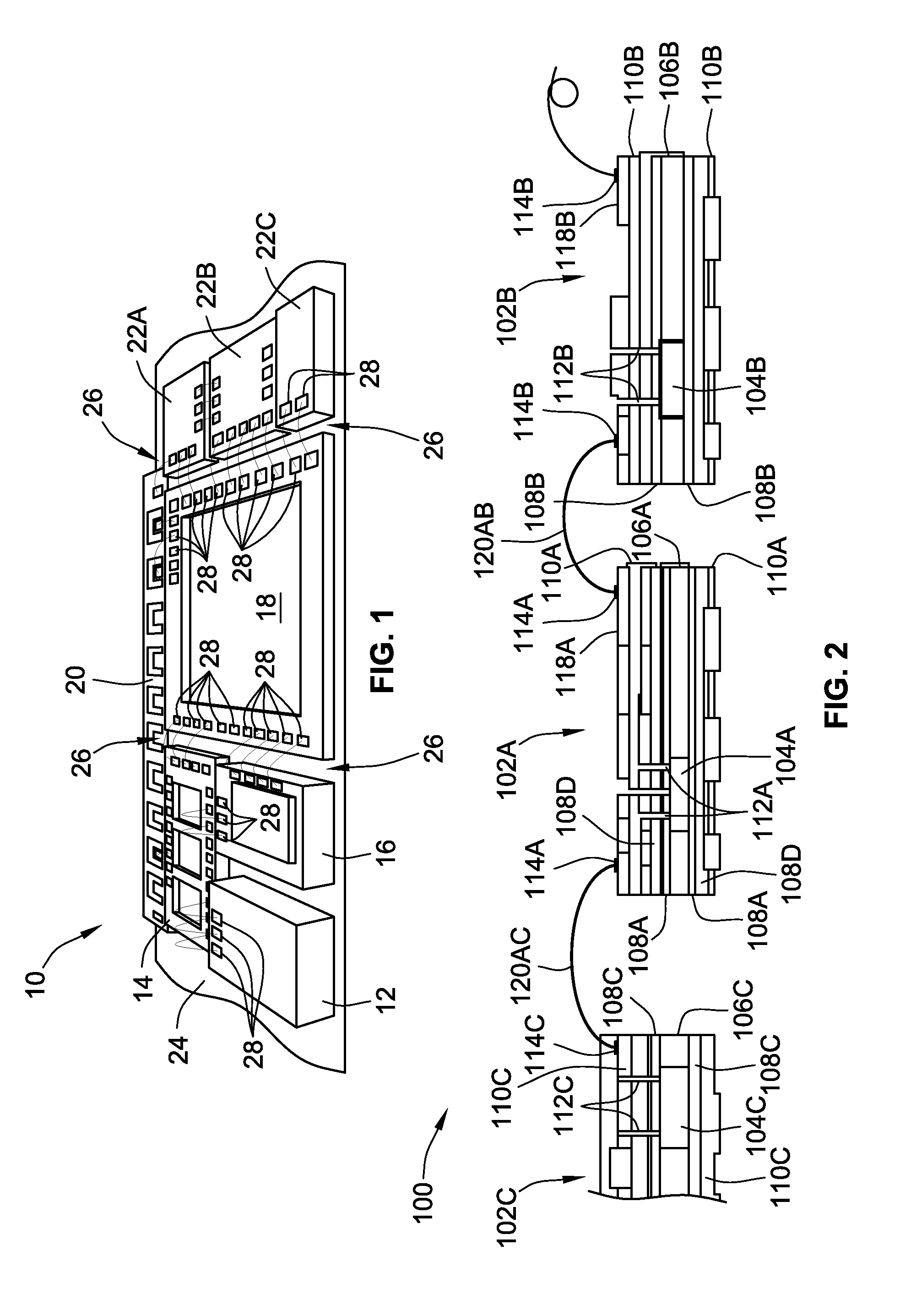
Referring now to the drawings, wherein like reference numerals refer to like components throughout the several views, FIG. 1 illustrates an example of a flexible integrated circuit (IC) system, designated generally as 10, which may be adapted as or integrated into an "extremely stretchable" IC apparatus. Many of the disclosed concepts are discussed with reference to the representative systems depicted in the drawings; the systems illustrated herein, however, are provided merely as exemplary applications by which the various inventive aspects and features of this disclosure can be applied. Thus, the novel aspects and features of the present disclosure are not per se limited to the particular arrangements and components presented in the drawings. Moreover, only selected components of the system(s) have been shown and will be described in additional detail hereinbelow. Nevertheless, the systems and devices discussed herein can include numerous additional and alternative features, and other well-known peripheral components, for example, for carrying out the various methods and functions disclosed herein. Some of the illustrated components are optional and, thus, can be removed.
The flexible IC system 10 of FIG. 1 comprises various electronic components (collectively referred to as "circuitry"), such as a laminated battery 12, a set of microchips 14, a sensor 16, a sensor hub 18, antenna 20, and an assortment of integrated passive devices (IPD) 22A, 22B and 22C. The circuitry is applied, secured, embedded or otherwise affixed to substrate 24, which is flexible--e.g., stretchable, bendable and/or compressible--as described herein. As such, the substrate 24 can be made of a plastic material or an elastomeric material, or combinations thereof. Examples of suitable flexible elastomers for the IC substrate material include polymeric organosilicon compounds (commonly referred to as "silicones"), including Polydimethylsiloxane (PDMS). Other non-limiting examples of materials suitable for the substrate 24 include polyimide, photopatternable silicon, SU8 polymer, PDS polydustrene, parylene and its derivatives and copolymers (parylene-N), ultrahigh molecular weight polyethylene, polyether ether ketones (PEEK), polyurethanes, polylactic acid, polyglycolic acid, polymer composites, silicones/siloxanes, polytetrafluoroethylene, polyamic acid, polymethyl acrylate, and combinations thereof. The substrate 24 can take on any possible number of shapes, sizes, and configurations. In the illustrated example, the substrate is substantially flat and, in some embodiments, configured to be an elongated sheet or strip.
The circuitry of FIG. 1 comprises one or more sensors 16 (also termed "sensor devices") to detect any of various parameters. These parameters can include, in any combination, thermal parameters (e.g., temperature), optical parameters (e.g., infrared energy), electrochemical and biochemical parameters, such as pH, enzymatic activity, blood components (e.g., glucose), ion concentrations, and protein concentrations, electrical parameters (e.g., resistance, conductivity, impedance, etc.), acoustic parameters, tactile parameters (e.g., pressure, surface characteristics, or other topographic features), etc. In this regard, one or more of the sensors 16 may be a thermocouple, a silicon band gap temperature sensor, a thin-film resistance temperature device, an LED emitter, a photodetector, a piezoelectric sensor, an ultrasonic sensor, an ion sensitive field effect transistor, etc. For some implementations, one or more of the sensors 16 can be coupled to a differential amplifier and/or a buffer and/or an analog to digital converter. The sensor hub 18, which may be in the nature of a microcontroller or digital signal processor (DSP), operates to integrate data signals from the sensor(s) 16 and process such signals. Signals from the sensor(s) 16 can be processed using multiplexing techniques, and can be switched into and processed by one or a few amplifier/logic circuits, including one or more of the microchips 14.
Battery 12 acts as a power source to supply power to the circuitry in the flexible IC system 10 of FIG. 1. Any suitable battery which is small in size and has a sufficiently long life with a suitable amp-hour capacity may be employed. It is also within the scope of this disclosure to employ alternative means for powering the system 10, including external power supplies. According to some embodiments, the flexible IC system 10 also includes a data transmission facility with an RF antenna 20 to wirelessly communicate with external devices. The antenna 20 can take on various forms, including a printed trace antenna coil with vias, which may be operable as a low frequency, high frequency or ultra-high frequency antenna. Other forms of wired and wireless signal transmission are also within the scope of this disclosure. Each integrated passive device (IPD) 22A-22C may comprise, as some non-limiting examples, a filter, a transformer, a photodiode, LED, TUFT, electrode, semiconductor, duplexer, coupler, phase shifter, thin-film device, circuit element, control elements, capacitors, resistors, inductors, buffer or other passive component. IPD's 22A-22C can be fabricated as standalone devices each having a silicon chip that may be connected to an active integrated circuit (e.g., a microprocessor).
For embodiments where the substrate 24 is stretchable or compressible, the illustrated circuitry is configured in applicable manners, such as those described herein, to be stretchable or compressible and/or to accommodate such stretching/compressing of the substrate 24. Similarly, for embodiments where the substrate 24 is bendable, but not necessarily stretchable, the illustrated circuitry is configured in applicable manners, such as those described herein, to be bendable and/or accommodate such bending of the substrate. For example, each of the illustrated modules or "islands" is connected to one or more adjacent modules with flexible wirebonded interconnects, some of which are designated generally as 26 in FIG. 1. The connection point of the individual interconnects to a device island may be anywhere along the device island edge, or may be at a point on the top surface of the device island (i.e., the surface opposite the substrate 24). The bond wires 26 are attached to externally mounted bond pads 28 on the modules and extend to a corresponding externally mounted bond pad 28 on an adjacent module. The bond wires can be attached through any known wirebonding technique, such as: ultrasonic bonding which uses a combination of pressure and ultrasonic vibration bursts to form a metallurgical cold weld; thermocompression bonding which uses a combination of pressure and elevated temperature to form a weld; and thermosonic bonding which uses a combination of pressure, elevated temperature, and ultrasonic vibration bursts to form a weld joint.
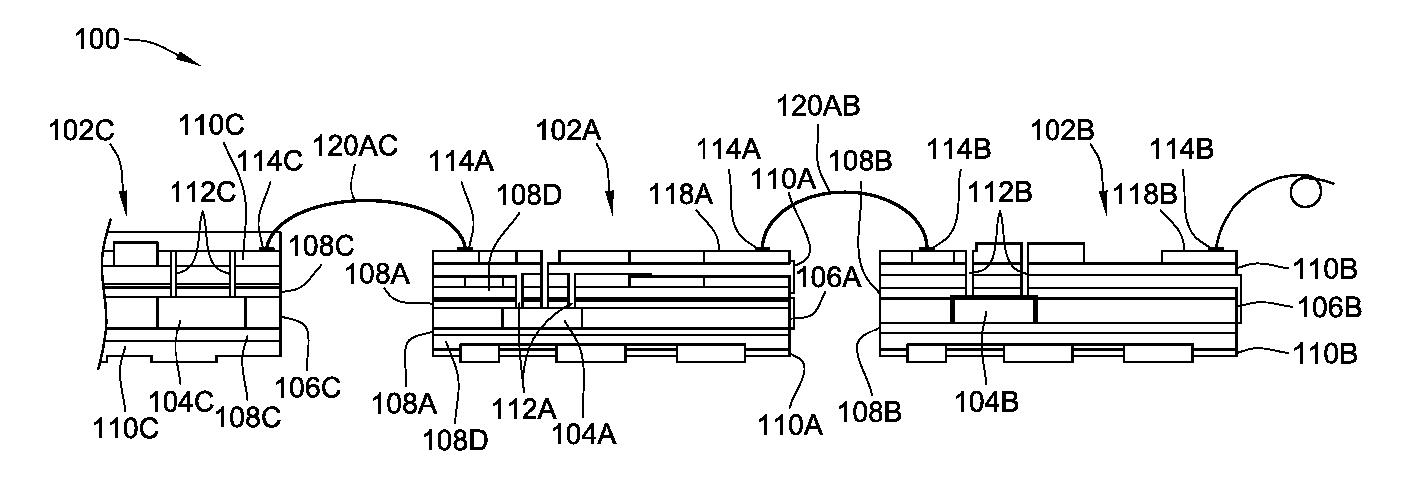
Turning next to FIG. 2, there is shown a cross-sectional illustration of a representative flexible electronic circuit system, designated generally as 100, with multi-layer IC modules connected via pliant wirebonded interconnects. While differing in appearance, the flexible IC system 100 of FIG. 2 can take on any of the various forms, optional configurations, and functional alternatives described herein with respect to the examples shown in FIGS. 1 and 3-5, and thus can include any of the corresponding options and features. Like the system 10 of FIG. 1, for example, the system 100 of FIG. 2 may be configured as an ultrathin, extremely stretchable integrated circuit system. Moreover, system 100 comprises an assortment of discrete devices--e.g., first, second and third discrete devices 102A, 102B and 102C--that are arranged in a "device island" arrangement and electrically coupled by pliant wirebonded interconnects. It is contemplated that the system 100 comprise greater or fewer than the three discrete devices shown in FIG. 2, each of which may take on alternative forms and configurations.
In the embodiment of FIG. 2, each of the discrete devices 102A-102C includes a flexible multi-layer integrated circuit (IC) package capable of performing one or more of the functions described herein. The multi-layer IC package of each discrete device, for example, includes a respective microchip--first, second and third microchips 104A, 104B and 104C--embedded in or on a respective flexible polymeric substrate--first, second and third substrates 106A, 106B and 106C. The polymeric substrates 106A-106C may be fabricated in any industry-recognized manner and from any of the materials described above with respect to the substrate 24 of FIG. 1. Optionally, the substrates 106A-106C may be fabricated from a liquid crystal polymer or a polyimide polymer, such as KAPTON.RTM. film available from DuPont.TM.. The polymeric substrate can have a thickness of about 60 .mu.m to about 85 .mu.m or, in some embodiments, about 25 .mu.m to about 50 .mu.m or, in some embodiments, about 7 .mu.m to about 10 .mu.m. Each substrate may also comprise a layer of a flexible polymer disposed on a layer of conductive material, such as copper, gold, aluminum, or some combination thereof. In an example, PCB metal layers can be patterned on opposing sides of the polymeric substrate 106A-106C.
One or more or all of the microchips 104A-104C may be a "thin chip" configuration with a thickness of about 2-7 .mu.m or, in some embodiments, a thickness of about 5-7 .mu.m or, in some embodiments, a thickness of about 3-5 .mu.m or, in some embodiments, a thickness of about 2-3 .mu.m. In the representative systems, methods and devices described herein, each thin chip can be one or more passive electronic devices and/or one or more active electronic devices. By comparison, a thin chip may be fabricated onto a silicon-based semiconductor die 104 with a thickness of approximately 35-50 .mu.m or, in some embodiments, a thickness of approximately 15-25 .mu.m or, in some embodiments, a thickness of approximately 10-15 .mu.m, for example. Non-limiting examples of devices that can be embedded according to any of the principles described herein include an amplifier, a transistor, a photodiode array, a photodetector, a sensor, a light-emitting device, a photovoltaic device, a semiconductor laser array, an optical imaging device, a logic gate array, a microprocessor, an opto-electronic device, a microelectromechanical device, a microfluidic device, a nanoelectromechanical device, a thermal device, or other device structures.
A pair of adhesive layers is disposed on opposing sides of the flexible polymeric substrates 106A-106C of the multi-layer IC package of each discrete device 102A-102C. In an example, the first flexible multi-layer IC package includes a first pair of adhesive layers 108A, each of which is attached to a respective side of the first polymeric substrate 106A. Likewise, the second flexible multi-layer IC package includes a second pair of adhesive layers 108B, each of which is attached to a respective side of the second polymeric substrate 106B. In addition, the third multi-layer IC package includes a third pair of adhesive layers 108C, each of which is attached to a respective side of the third polymeric substrate 106C. Each layer of adhesive can have a thickness of about 8 .mu.m to about 35 .mu.m or, in some embodiments, about 20 .mu.m to about 35 .mu.m or, in some embodiments, about 12 .mu.m to about 15 .mu.m or, in some embodiments, about 8 .mu.m to about 10 .mu.m. The adhesive can be a conductive adhesive or a non-conductive (dielectric) adhesive that is configured to withstand the temperatures of further processing. Conductive adhesive can be used to establish electrical communication between the conductive material of the substrate and conductive contact pads on the top surface of the thin chip. In an example, the adhesive layers 108A-108C can be a fluropolymer adhesive, a polyimide (PI) adhesive, an epoxy adhesive, or an acrylic adhesive, such as PYRALUX.RTM. Bond-Ply available from DuPont.TM.. Optionally, the material of adhesive layer can be selected such that it is a non-conductive electrical insulator capable of adhering the adjacent layers. Each multi-layer IC package may optionally include additional adhesive layers, as represented in FIG. 2 by the additional pair of adhesive layers 108D attached to the outer surfaces of the first adhesive layers 108A. With the additional layers, the total thickness of the adhesive may be as large as 85 .mu.m, according to some embodiments.
As illustrated in FIG. 2, the flexible multi-layer IC package of each discrete device 102A-102C further comprises a pair of electrically conductive (polymeric or metallic) layers on opposing sides of the flexible polymeric substrates 106A-106C. For example, the first flexible multi-layer IC package includes a first pair of metallic sheets 110A attached via the first adhesive layers 108A to the first flexible polymeric substrate 106A. Likewise, the second multi-layer IC package includes a second pair of metallic sheets 110B attached via the second adhesive layers 108B to the second flexible polymeric substrate 106B. In addition, the third multi-layer IC package includes a third pair of metallic sheets 110C attached via the third adhesive layers 108C to the third flexible polymeric substrate 106C. Each metallic sheet can have a thickness of about 5 .mu.m to about 20 .mu.m or, in some embodiments, about 15 .mu.m to about 20 .mu.m or, in some embodiments, about 10 .mu.m to about 12 .mu.m or, in some embodiments, about 5 .mu.m to about 8 .mu.m. Electrically conductive metallic layers can be fabricated, for example, from copper or aluminum or a combination thereof.
One or more vias can be generated as channels (e.g., with a laser drill) extending through outer layers of each flexible multi-layer IC package to allow for conductive connections between different layers of the multi-layer stack. In FIG. 2, for example, the first multi-layer IC package includes a first pair of vias 112A that extend through a (top) conductive sheet 110A and corresponding (top) adhesive layer 108A to the first microchip 104A. In the same vein, the second multi-layer IC package includes a second pair of vias 112B that extend through a (top) conductive sheet 110B and corresponding (top) adhesive layer 108B to the second microchip 104B. Likewise, the third multi-layer IC package includes a third pair of vias 112C that extend through a (top) conductive sheet 110C and corresponding (top) adhesive layer 108C to the second microchip 104C. Once these vias have been created, the vias can be electroplated or filled through sputtering or other known technique to create electrical connections from the top conductive layer to an electrical contact pad of the chip. The conductive layers can then be patterned and an overlay can be applied to the outer surface of each conductive layer. In some implementations, the overlay is non-conductive polymer.
On the outer surface of each discrete device 102A-102C are one or more electrical connection pads 114A, 114B and 114C, respectively, for electrically coupling with adjacent devices. By way of non-limiting example, the first discrete device 102A is shown with two electrical connection pads 114A on the top surface of the first multi-layer IC package to provide electrical communication with the first microchip 104A, while the second discrete device 102B is shown with two electrical connection pads 114B on the top surface of the second multi-layer IC package to provide electrical communication with the second microchip 104B. Similarly, the third discrete device 102C is shown with at least one electrical connection pad 114C on the top surface of the third multi-layer IC package to provide electrical communication with the third microchip 104C. Optionally, the first discrete device 102A includes a corresponding set of surface-mount-technology (SMT) components 118A mounted on the first outer surface of the first flexible multi-layer IC package, and the second discrete device 102B includes a second set of SMT components 118B mounted on the outer surface of the second flexible multi-layer IC package.
It is contemplated that one or more or all of the illustrated multi-layer IC packages comprise additional or fewer layers than the sandwich constructions shown in FIG. 2. It should also be noted that the use of the term "layer" in the description and claims does not necessarily require that particular segment of the sandwich construction be continuous or span the entirety of (i.e., be coextensive with) all remaining layers unless otherwise explicitly stated in the claims. While preferable in some applications, it is not necessary in practice that the adhesive layers of each package be fabricated from the same material and the conductive layers be fabricated from the same material. Moreover, the individual packages may be vacuum laminated as discrete, unitary structures prior to electrical coupling with one or more adjacent devices.
Discrete flexible interconnects are attached to and electrically connect the electrical connection pad of one discrete device to the electrical connection pad of another discrete device. In accord with the flexible IC system 100 of FIG. 2, a discrete flexible interconnect in the form of a curvilinear wirebond 120AB is attached or coupled to and electrically connects a first (right) electrical connection pad 114A of the first discrete device 102A to a second (left) electrical connection pad 114B of the second discrete device 102B. Likewise, a discrete flexible interconnect in the form of a curvilinear wirebond 120AC is attached or coupled to and electrically connects a first (left) electrical connection pad 114A of the first discrete device 102A to a third (right) electrical connection pad 114C of the third discrete device 102C. In the illustrated example, the flexible interconnects each comprise one or more pliant metal wires, e.g., made from copper or gold with a circular cross-section, each of which may comprise in-plane loops (one of which can be seen to the far right in FIG. 2) or out-of-plane-loops, or both, that increase the elasticity of the wire. Examples of such in-plane loops and out-of-plane-loops are depicted and described in commonly owned U.S. Pat. No. 8,536,667, which is incorporated herein by reference in its entirety and for all purposes. Any in-plane or out-of-plane loops help to ensure a sufficient degree of stretchability and flexibility. These wirebonded interconnects are fabricated separately from and subsequently attached to the discrete flexible IC modules (e.g., using thermosonic wirebonding techniques). Proper solder joints and welds are created to attach the interconnects to the externally mounted pads and thereby ensure reliability of the interconnects.
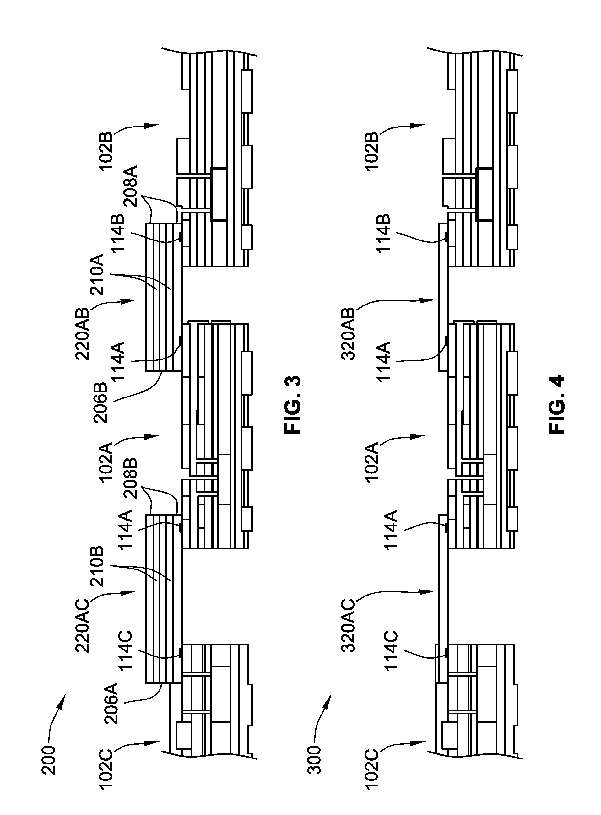
FIG. 3 illustrates another representative flexible electronic circuit system, designated generally as 200, with multi-layer IC modules that are connected via pliant multi-layer polymeric interconnects. Like reference numerals are used in FIGS. 3 and 4 to indicate similar structure from FIG. 2. For example, the system 200 of FIG. 3 and the system 300 of FIG. 4 each comprises a similar assortment of discrete devices--e.g., first, second and third discrete devices 102A, 102B and 102C--that are arranged in a "device island" arrangement and electrically coupled by pliant electrical interconnects. Moreover, the flexible IC systems 200 and 300 can take on any of the various forms, optional configurations, and functional alternatives described herein with respect to the other examples shown in the figures, and vice versa, unless explicitly or logically prohibited.
Discrete flexible interconnects mechanically attach to and electrically connect the electrical connection pads of one discrete device to the electrical connection pads of other discrete devices in FIG. 3. The top side of each module 102A-102C is provided with a connection pad 114A, 114B, 114C for electrically connecting to other packages. According to the illustrated example, a first discrete flexible interconnect in the form of a pliant multi-layer semiconductor 220AB is attached or coupled to and electrically connects a first (right) electrical connection pad 114A of the first discrete device 102A to a second (left) electrical connection pad 114B of the second discrete device 102B. Likewise, a second discrete flexible interconnect in the form of a pliant multi-layer semiconductor 220AC is attached to and electrically connects a first (left) electrical connection pad 114A of the first discrete device 102A to a third (right) electrical connection pad 114C of the third discrete device 102C. According to some embodiments, the first discrete flexible interconnect in the form of a pliant multi-layer semiconductor 220AB and the second discrete flexible interconnect in the form of a pliant multi-layer semiconductor 220AC are attached to respective electrical connection pads 114A, 114B, 114C using a traditional solder attach.
The discrete flexible IC modules 102A-102C are built as separate packages with the IC embedded in the substrate. Interconnects 220AB, 220AC are manufactured in separate PCB flex substrates from the IC modules 102A-102C, and can be cut with a serpentine or other non-linear shape to provide stretchability. Examples of interconnects with serpentine shapes are depicted and described in U.S. Pat. Nos. 8,389,862 and 8,729,524, both of which are incorporated herein by reference in their respective entireties and for all purposes. The top side of each module 102A-102C is provided with a connection pad 114A, 114B, 114C for electrically connecting to other packages. Any SMT components required for a particular IC can be mounted on the top surface of the package. It is possible to stack flexible modules on top of each other similar to Package-on-Package (PoP) technology using appropriate solder, etc. Examples of semiconductor devices having package-on-package (POP) configurations are disclosed in U.S. Pat. Nos. 7,696,618 and 7,250,675, both of which are incorporated herein by reference in their respective entireties. In so doing, the input-output connection points (I/Os) for each package can be minimized so as to restrict the number of required interconnections.
The flexible multi-layer IC package of the first discrete device 102A, the flexible multi-layer IC package of the second discrete device 102B, and the multi-layer semiconductors of each flexible interconnect 220AB, 220AC may all comprise common layers of materials, according to some embodiments. For instance, according to some embodiments, each interconnect 220AB, 220AC comprises a polymeric substrate 206A and 206B, respectively, that may be fabricated from a liquid crystal polymer or a polyimide polymer, such as KAPTON.RTM. film. According to some embodiments, the flexible interconnects 220AB, 220AC further comprise a pair of electrically conductive (polymeric or metallic) layers 210A and 210B, respectively, on opposing sides of the flexible polymeric substrates 206A, 206B. These electrically conductive layers can be fabricated, for example, from copper or aluminum or a combination thereof. First and second pairs of adhesive layers 208A and 208B are disposed on opposing sides of the flexible polymeric substrates 206A, 206B, respectively, covering one of the conductive layers 210A, 210B. Similar to the adhesive layers 108A-108C of the discrete devices 102A-102C, the adhesive layers 208A, 208B of the flexible interconnects 220AB, 220AC can be a fluropolymer adhesive, a polyimide (PI) adhesive, an epoxy adhesive, or an acrylic adhesive, such as PYRALUX.RTM. Bond-Ply.
FIG. 4 illustrates yet another representative flexible electronic circuit system, designated generally as 300, this time utilizing pliant conductive-paste-based interconnects to connect the discrete multi-layer IC modules. According to the illustrated example, a first discrete flexible interconnect in the form of a conductive substrate fabricated from an electrically conductive paste 320AB is attached or coupled to and electrically connects a first (right) electrical connection pad 114A of the first discrete device 102A to a second (left) electrical connection pad 114B of the second discrete device 102B. Likewise, a second discrete flexible interconnect in the form of a conductive substrate fabricated from an electrically conductive paste 320AC is attached or coupled to and electrically connects a first (left) electrical connection pad 114A of the first discrete device 102A to a third (right) electrical connection pad 114C of the third discrete device 102C. Each flexible interconnect 320AB, 320AC may comprise a web of metallic interconnects (e.g., copper or gold or a conductive polymer or paste) that printed or otherwise patterned, for example, using screen print or ink jet printing techniques onto the substrate.
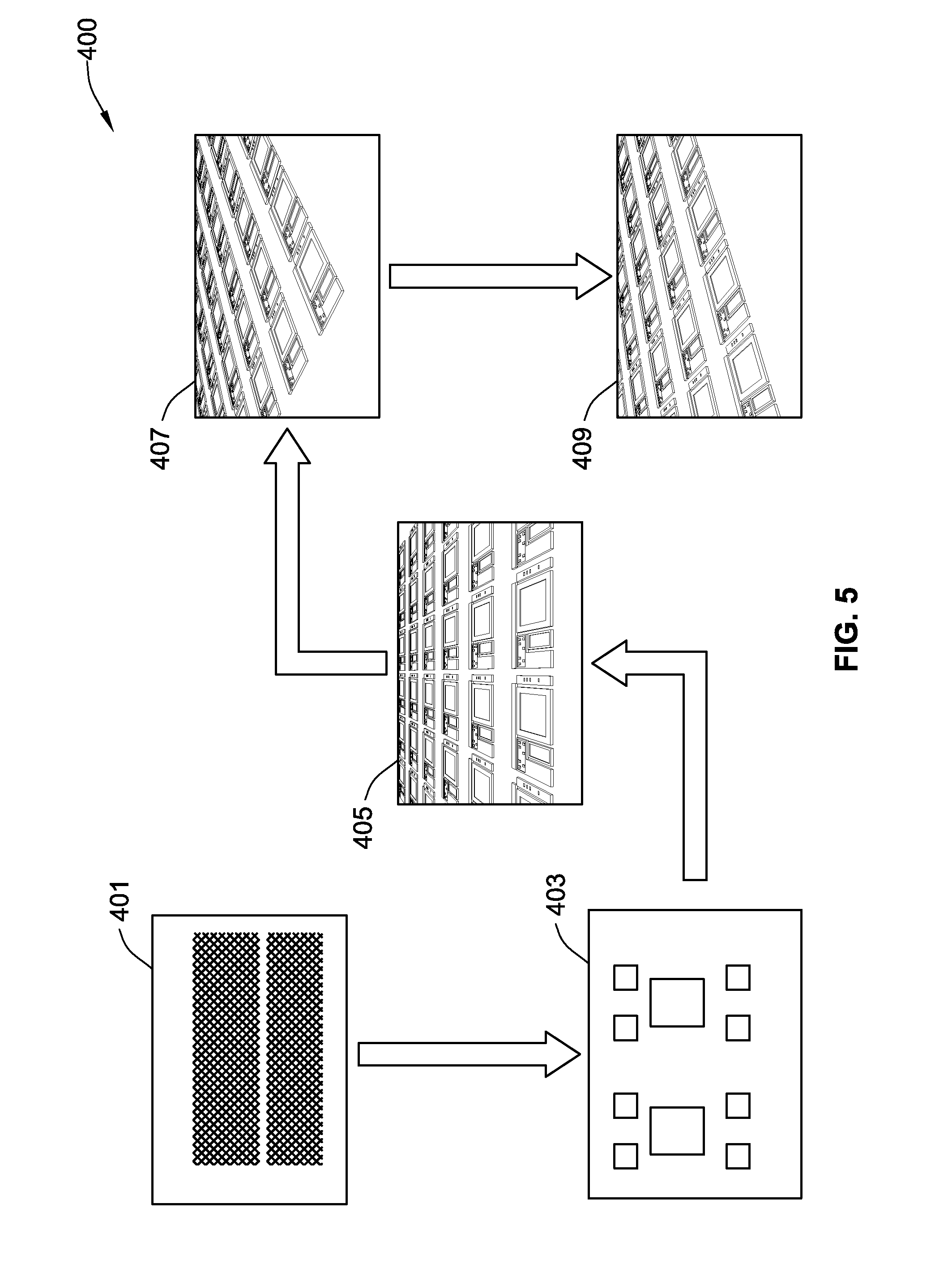
FIG. 5 illustrates a representative method 400 for manufacturing flexible integrated circuits. This method will be described with reference to the various configurations and features shown in FIGS. 1 through 4 of the drawings; such reference is being provided purely by way of explanation and clarification. At block 401, the method 400 includes embedding a thin die in large panels, punching out known good flexible parts or "KGFP," and sorting into waffle trays. Thus, the individual circuits can be tested before being punched out thereby reducing the potential for distributing malfunctioning parts. Next, the method 400 includes picking and placing the flex packages (e.g., the KGFP's are identified and sorted while any malfunctioning circuits are left) onto temporary rigid substrates (reusable substrate with disposable adhesive), as indicated at block 403. The adhesive strength can be modulated by light and/or heat. At block 405, wirebond flex package assemblies are placed on rigid substrates as a temporary carrier for copper wirebonding. The method 400 proceeds to block 407 to encapsulate the top side of the devices and remove the temporary substrate from the bottom. Block 409 includes encapsulating the bottom side of the devices and die cutting.
Also presented herein is a method for assembling flexible integrated circuits. This method includes, in any logical order and any logical combination: providing a first discrete device with a first flexible multi-layer integrated circuit (IC) package including a first outer surface with a first electrical connection pad; providing a second discrete device with a second flexible multi-layer integrated circuit (IC) package including a second outer surface with a second electrical connection pad; and electrically connecting a discrete flexible interconnect to the first electrical connection pad of the first discrete device and the second electrical connection pad of the second discrete device. The flexible interconnect may comprise one or more pliant metal wires. Optionally or alternatively, the flexible interconnect comprises a pliant multi-layer semiconductor or a conductive substrate fabricated from an electrically conductive paste. The first multi-layer IC package may comprise a first microchip embedded in or on a first flexible polymeric substrate, a first adhesive layer on the first flexible polymeric substrate, and a first conductive sheet attached to the first flexible polymeric substrate by the first adhesive layer. Likewise, the second flexible multi-layer IC package may comprise a second microchip embedded in or on a second flexible polymeric substrate, a second adhesive layer on the second flexible polymeric substrate, and a second conductive sheet attached to the second flexible polymeric substrate by the first adhesive layer.
In some embodiments, the aforementioned methods each includes at least those steps shown in FIG. 5 and/or those steps enumerated above. It is also within the scope and spirit of the present disclosure to omit steps, include additional steps, and/or modify the order presented herein. It should be further noted that each of the foregoing methods can be representative of a single sequence of related steps; however, it is expected that each of these methods will be practiced in a systematic and repetitive manner.
The present disclosure is not limited to the precise construction and compositions disclosed herein; any and all modifications, changes, and variations apparent from the foregoing descriptions are within the spirit and scope of the disclosure as defined in the appended claims. Moreover, the present concepts expressly include any and all combinations and subcombinations of the preceding elements and aspects.
* * * * *
References
D00000
D00001
D00002
D00003
XML
uspto.report is an independent third-party trademark research tool that is not affiliated, endorsed, or sponsored by the United States Patent and Trademark Office (USPTO) or any other governmental organization. The information provided by uspto.report is based on publicly available data at the time of writing and is intended for informational purposes only.
While we strive to provide accurate and up-to-date information, we do not guarantee the accuracy, completeness, reliability, or suitability of the information displayed on this site. The use of this site is at your own risk. Any reliance you place on such information is therefore strictly at your own risk.
All official trademark data, including owner information, should be verified by visiting the official USPTO website at www.uspto.gov. This site is not intended to replace professional legal advice and should not be used as a substitute for consulting with a legal professional who is knowledgeable about trademark law.