Three-dimensional semiconductor wafer
Wang , et al.
U.S. patent number 10,290,706 [Application Number 15/665,690] was granted by the patent office on 2019-05-14 for three-dimensional semiconductor wafer. This patent grant is currently assigned to LuoYang HongTai Semiconductor Co., Ltd. The grantee listed for this patent is LuoYang HongTai Semiconductor Co., Ltd. Invention is credited to Jianwei Deng, Zhenguo Wang, Zhilin Zhang.


| United States Patent | 10,290,706 |
| Wang , et al. | May 14, 2019 |
Three-dimensional semiconductor wafer
Abstract
A three-dimensional semiconductor wafer relates to a semiconductor wafer, including a raw semiconductor wafer, at least one connection layer, a conduction layer and a protection layer, wherein the protection layer is arranged on the conduction layer; the connection layer is inserted into a bottom surface or/and a top surface of the raw semiconductor wafer; and the conduction layer is arranged on the bottom surface of the raw semiconductor wafer.
| Inventors: | Wang; Zhenguo (Henan, CN), Deng; Jianwei (Henan, CN), Zhang; Zhilin (Henan, CN) | ||||||||||
|---|---|---|---|---|---|---|---|---|---|---|---|
| Applicant: |
|
||||||||||
| Assignee: | LuoYang HongTai Semiconductor Co.,
Ltd (Luoyang, Henan, CN) |
||||||||||
| Family ID: | 57274691 | ||||||||||
| Appl. No.: | 15/665,690 | ||||||||||
| Filed: | August 1, 2017 |
Prior Publication Data
| Document Identifier | Publication Date | |
|---|---|---|
| US 20170330936 A1 | Nov 16, 2017 | |
Foreign Application Priority Data
| Aug 29, 2016 [CN] | 2016 1 0736822 | |||
| Current U.S. Class: | 1/1 |
| Current CPC Class: | G06T 15/10 (20130101); H01L 23/31 (20130101); H01L 29/0684 (20130101); H01L 23/52 (20130101); H01L 23/485 (20130101); H01L 21/02002 (20130101); H01L 29/78651 (20130101); H01L 29/0634 (20130101); H01L 29/7802 (20130101) |
| Current International Class: | G06T 15/10 (20110101); H01L 29/06 (20060101); H01L 23/485 (20060101); H01L 23/52 (20060101); H01L 23/31 (20060101); H01L 29/786 (20060101); H01L 29/78 (20060101) |
References Cited [Referenced By]
U.S. Patent Documents
| 6538309 | March 2003 | Hotta |
Claims
What is claimed is:
1. A three-dimensional semiconductor wafer, comprising a raw semiconductor wafer, a connection layer, a conduction layer and a protection layer, wherein the raw semiconductor wafer is cylindrical; the protection layer is arranged on the conduction layer; the connection layer is inserted into a bottom surface or/and a top surface of the raw semiconductor wafer; and the conduction layer is arranged on the bottom surface of the raw semiconductor wafer.
2. The three-dimensional semiconductor wafer, as recited in claim 1, wherein an amount of the connection layer is at least one.
3. The three-dimensional semiconductor wafer, as recited in claim 2, wherein the connection layer comprises a plurality of connection parts; a first end of each connection part is inserted into the raw semiconductor wafer, and a second end of each connection part is level with the bottom surface or the top surface of the raw semiconductor wafer; the connection parts are prismatic, cylindrical, spherical or ellipsoidal; and the connection parts are arranged inside the raw semiconductor wafer in a form of array.
4. The three-dimensional semiconductor wafer, as recited in claim 3, wherein the protection layer is connected to the conduction layer and the protection layer is a SiO.sub.2 layer.
5. The three-dimensional semiconductor wafer, as recited in claim 2, wherein the protection layer is connected to the conduction layer and the protection layer is a SiO.sub.2 layer.
6. The three-dimensional semiconductor wafer, as recited in claim 1, wherein the connection layer comprises a plurality of connection parts; a first end of each connection part is inserted into the raw semiconductor wafer, and a second end of each connection part is level with the bottom surface or the top surface of the raw semiconductor wafer; the connection parts are prismatic, cylindrical, spherical or ellipsoidal; and the connection parts are arranged inside the raw semiconductor wafer in a form of array.
7. The three-dimensional semiconductor wafer, as recited in claim 6, wherein: the raw semiconductor wafer is defined as an N- region, which has a conduction type of N-type; the connection layer is defined as an N+ region, which has the conduction type of N-type; for the array-distributed connection parts, first ends are inserted into the raw semiconductor wafer, and second ends are connected to each other on the bottom surface of the raw semiconductor wafer through the conduction layer; the conduction layer is defined as the N+ region, which has the conduction type of N-type; and the protection layer is arranged on the conduction layer at the bottom surface of the raw semiconductor wafer.
8. The three-dimensional semiconductor wafer, as recited in claim 7, wherein the protection layer is connected to the conduction layer and the protection layer is a SiO.sub.2 layer.
9. The three-dimensional semiconductor wafer, as recited in claim 6, wherein: the raw semiconductor wafer is defined as an N- region, which has a conduction type of N-type; the connection layer is defined as a P+ region, which has a conduction type of P-type; for the array-distributed connection parts, first ends are inserted into the raw semiconductor wafer, and second ends are connected to each other on the bottom surface of the raw semiconductor wafer through the conduction layer; the conduction layer is defined as the P+ region, which has the conduction type of P-type; and the protection layer is arranged on the conduction layer at the bottom surface of the raw semiconductor wafer.
10. The three-dimensional semiconductor wafer, as recited in claim 9, wherein the protection layer is connected to the conduction layer and the protection layer is a SiO.sub.2 layer.
11. The three-dimensional semiconductor wafer, as recited in claim 6, wherein: the raw semiconductor wafer is defined as an N.sup.- region, which has a conduction type of N-type; the connection layer defined as a P.sup.+ region, which has a conduction type of P-type; for the array-distributed connection parts, first ends are inserted into the raw semiconductor wafer, and second ends are connected to each other on the bottom surface of the raw semiconductor wafer through the conduction layer; the conduction layer is defined as an N.sup.+ region, which has the conduction type of N-type; and the protection layer is arranged on the conduction layer at the bottom surface of the raw semiconductor wafer.
12. The three-dimensional semiconductor wafer, as recited in claim 11, wherein the protection layer is connected to the conduction layer and the protection layer is a SiO.sub.2 layer.
13. The three-dimensional semiconductor wafer, as recited in claim 6, wherein: the raw semiconductor wafer is defined as an N.sup.- region, which has a conduction type of N-type; the connection layer is defined as a P.sup.+ region, which has a conduction type of P-type; for the array-distributed connection parts, first ends are inserted into the raw semiconductor wafer, and second ends are level with the top surface of the raw semiconductor wafer; the conduction layer is defined as an N.sup.+ region, which has the conduction type of N-type; and the protection layer is arranged on the conduction layer at the bottom surface of the raw semiconductor wafer.
14. The three-dimensional semiconductor wafer, as recited in claim 13, wherein the protection layer is connected to the conduction layer and the protection layer is a SiO.sub.2 layer.
15. The three-dimensional semiconductor wafer, as recited in claim 6, wherein the protection layer is connected to the conduction layer and the protection layer is a SiO.sub.2 layer.
16. The three-dimensional semiconductor wafer, as recited in claim 1, wherein the protection layer is arranged on an outer surface of the conduction layer.
17. The three-dimensional semiconductor wafer, as recited in claim 16, wherein the protection layer is connected to the conduction layer and the protection layer is a SiO.sub.2 layer.
18. The three-dimensional semiconductor wafer, as recited in claim 1, wherein the protection layer is connected to the conduction layer and the protection layer is a SiO.sub.2 layer.
Description
CROSS REFERENCE OF RELATED APPLICATION
The application claims priority under 35 U.S.C. 119(a-d) to CN 201610736822.5, filed Aug. 29, 2016.
BACKGROUND OF THE PRESENT INVENTION
Field of Invention
The present invention relates to the field of semiconductor wafers. More particularly, the present invention relates to three-dimensional semiconductor wafers.
Description of Related Arts
Generally, the wafer material applied in the production of semiconductor chips is mainly a single crystal epitaxial wafer or a single crystal polished wafer. The epitaxial wafer is obtained through forming an epitaxial layer on the single crystal polished wafer. The single crystal polished wafer serves as a substrate layer to support the epitaxial layer, and the epitaxial layer is used to support the blocking voltage of power semiconductor devices.
In order to make a breakthrough to the silicon limit and achieve huge improvement for the design of high blocking voltage power devices with reduced specific on-resistance or conduction loss, superjunction (SJ) power devices with a voltage sustaining layer composed of alternating p and n doped region become popular. In order to form a three-dimensional sustaining layer, the methods of multiple epitaxy and deep trench are used. However, these manufacture processes of a SJ sustaining layer are complicated and expensive.
SUMMARY OF THE PRESENT INVENTION
An object of the present invention is to provide a three-dimensional semiconductor wafer.
The three-dimensional semiconductor wafer comprises a raw semiconductor wafer, at least one connection layer, a conduction layer and a protection layer. The protection layer is arranged on the conduction layer. The connection layer is inserted into a bottom surface or/and a top surface of the raw semiconductor wafer. The conduction layer is arranged on the bottom surface of the raw semiconductor wafer.
Preferably, the raw semiconductor wafer is cylindrical.
Preferably, the connection layer comprises a plurality of connection parts. A first end of each connection part is inserted into the raw semiconductor wafer, and a second end of each connection part is level with the bottom surface or the top surface of the raw semiconductor wafer.
Preferably, the connection parts are prismatic, cylindrical, spherical or ellipsoidal, and the connection parts are arranged inside the raw semiconductor wafer in a form of array.
Preferably, the protection layer is arranged on an outer surface of the conduction layer.
Through adopting the above technical solutions, the present invention has following beneficial effects.
The present invention provides the three-dimensional semiconductor wafer, comprising the raw semiconductor wafer, the connection layer, the conduction layer and the protection layer. The three-dimensional semiconductor wafer provided by the present invention can not only replace two-dimensional semiconductor wafer materials such as a single crystal epitaxial wafer, but also provide a design basis for high performance semiconductor devices.
BRIEF DESCRIPTION OF THE DRAWINGS
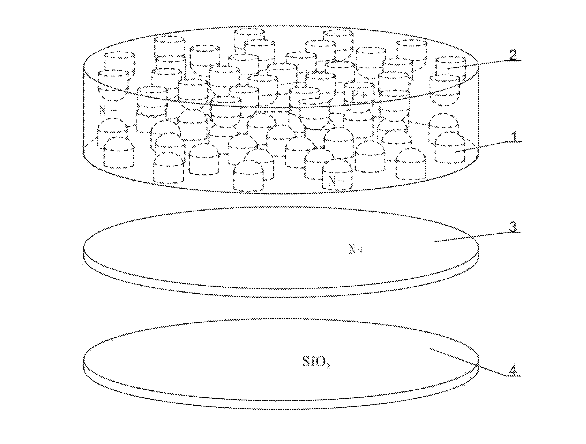
FIG. 1 is an exploded view of a three-dimensional semiconductor wafer according to preferred embodiments of the present invention.
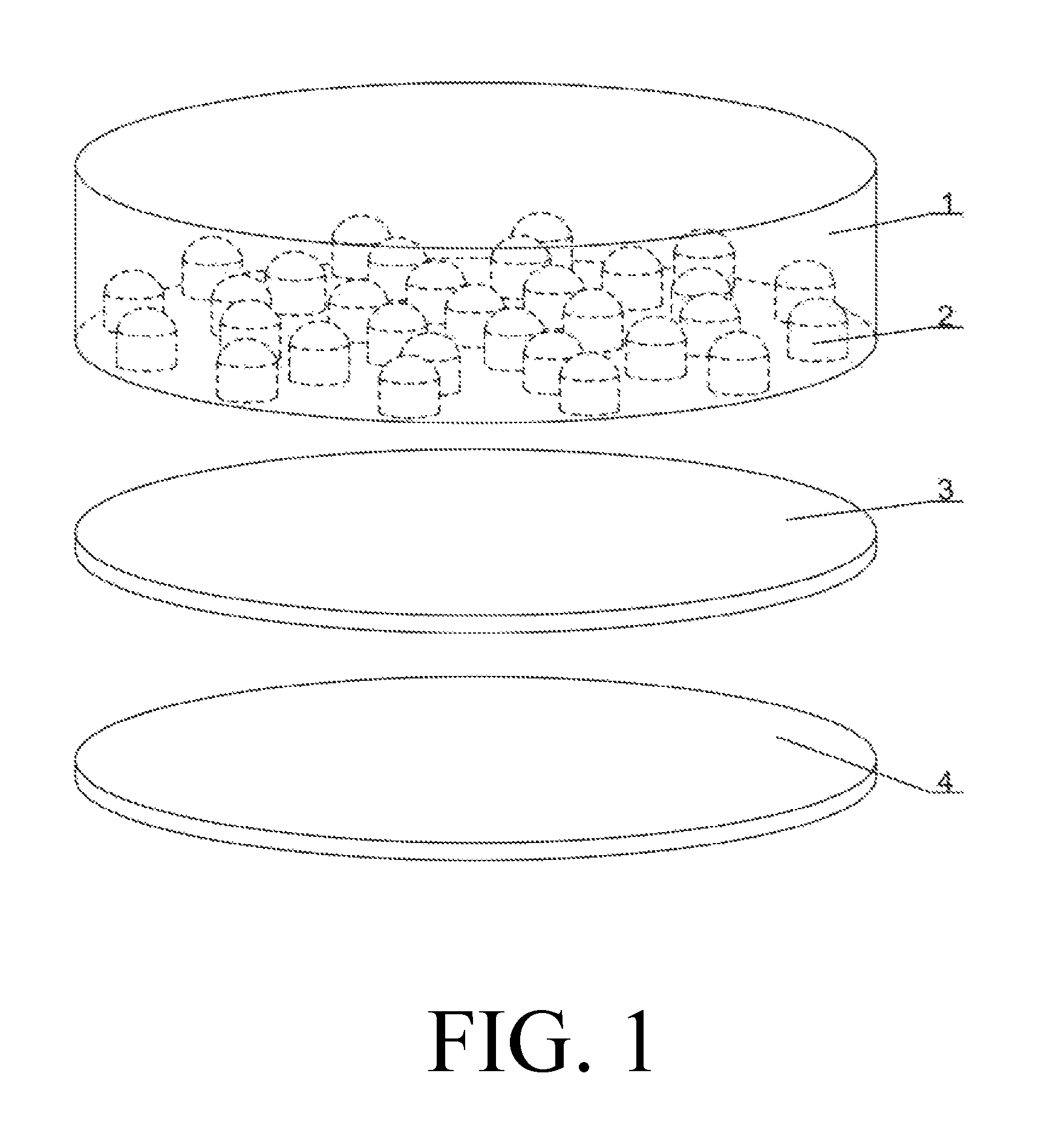
FIG. 2 is an exploded view of an (N.sup.-/N.sup.+/N.sup.+)-typed three-dimensional semiconductor wafer according to a first preferred embodiment of the present invention.
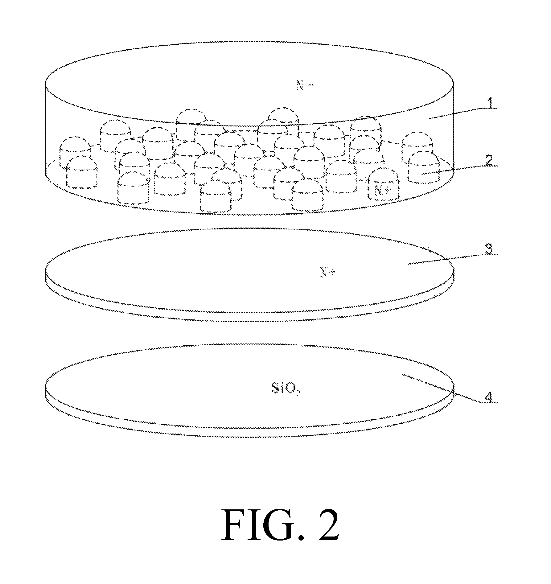
FIG. 3 is an exploded view of an (N.sup.-/P.sup.+/P.sup.+)-typed three-dimensional semiconductor wafer according to a second preferred embodiment of the present invention.
FIG. 4 is an exploded view of an (N.sup.-/N.sup.+/P.sup.+)-typed three-dimensional semiconductor wafer according to a third preferred embodiment of the present invention.
FIG. 5 is an exploded view of an (N.sup.-/P.sup.+/N.sup.+)-typed three-dimensional semiconductor wafer according to a fourth preferred embodiment of the present invention.
FIG. 6 is an exploded view of a (P.sup.-/P.sup.+/P.sup.+)-typed three-dimensional semiconductor wafer according to a fifth preferred embodiment of the present invention.
FIG. 7 is an exploded view of a (P.sup.-/N.sup.+/N.sup.+)-typed three-dimensional semiconductor wafer according to a sixth preferred embodiment of the present invention.
FIG. 8 is an exploded view of an (N.sup.-/P.sup.+ top surface/N.sup.+)-typed three-dimensional semiconductor wafer according to a seventh preferred embodiment of the present invention.
FIG. 9 is an exploded view of an (N.sup.-/P.sup.+ top surface/N.sup.+ bottom surface/N.sup.+)-typed three-dimensional semiconductor wafer according to an eighth preferred embodiment of the present invention.
DETAILED DESCRIPTION OF THE PREFERRED EMBODIMENT
A three-dimensional semiconductor wafer comprises a raw semiconductor wafer 1, at least one connection layer, a conduction layer 3 and a protection layer 4, wherein: the protection layer 4 is arranged on the conduction layer 3; the connection layer is inserted into a bottom surface or/and a top surface of the raw semiconductor wafer 1; the conduction layer is arranged on the bottom surface of the raw semiconductor wafer 1; the raw semiconductor wafer 1 is cylindrical; the connection layer comprises a plurality of connection parts 2; a first end of each connection part 2 is inserted into the raw semiconductor wafer 1, and a second end of each connection part 2 is level with the bottom surface or the top surface of the raw semiconductor wafer 1; the connection parts 2 are prismatic, cylindrical, spherical or ellipsoidal; the connection parts 2 are arranged inside the raw semiconductor wafer 1 in a form of array; and the protection layer 4 is arranged on an outer surface of the conduction layer 3.
For the three-dimensional semiconductor wafer provided by the present invention, according to types of semiconductors of different power, a conduction type of the raw semiconductor wafer 1, the connection layer, and the conduction layer 3 can be respectively selected as N-type or P-type, wherein the bottom surface of the raw semiconductor wafer 1 can be produced according to requirements of a chip.
First Preferred Embodiment
As shown in FIG. 2, the raw semiconductor wafer 1 is a lightly doped N-type region, namely an N.sup.- region; the connection layer is a heavily doped N-type region, namely an N.sup.+ region; for the array-distributed connection parts 2, the first ends are inserted into the raw semiconductor wafer 1, and the second ends are connected to each other on the bottom surface of the raw semiconductor wafer 1 through the conduction layer 3; the conduction layer 3 is a heavily doped N-type region, namely the N.sup.+ region; and the protection layer 4 is arranged on the conduction layer 3 at the bottom surface of the raw semiconductor wafer 1.
Second Preferred Embodiment
As shown in FIG. 3, the raw semiconductor wafer 1 is a lightly doped N-type region, namely an N.sup.- region; the connection layer is a heavily doped P-type region, namely a P.sup.+ region; for the array-distributed connection parts 2, the first ends are inserted into the raw semiconductor wafer 1, and the second ends are connected to each other on the bottom surface of the raw semiconductor wafer 1 through the conduction layer 3; the conduction layer 3 is a heavily doped P-type region, namely the P.sup.+ region; and the protection layer 4 is arranged on the conduction layer 3 at the bottom surface of the raw semiconductor wafer 1.
Third Preferred Embodiment
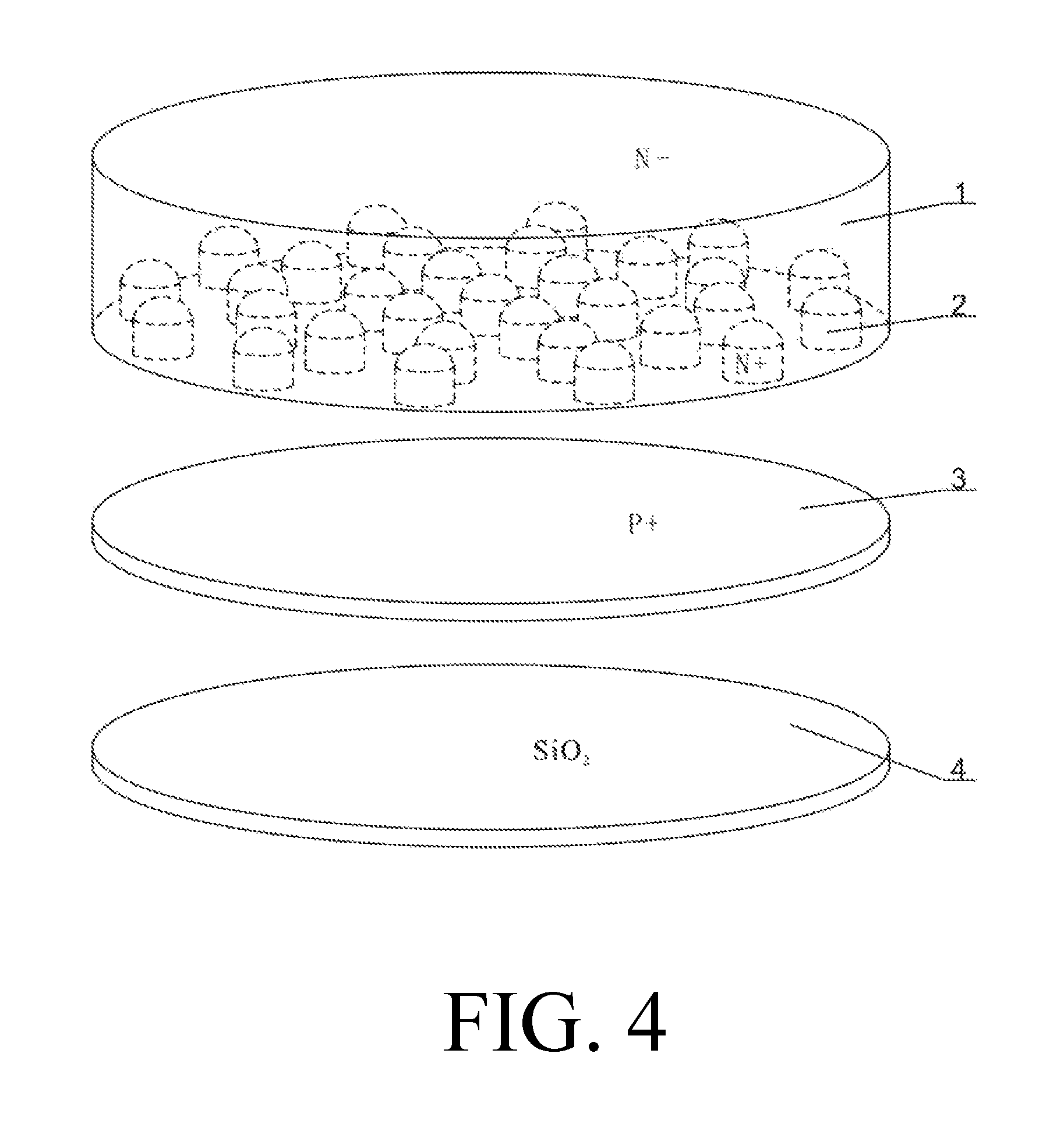
As shown in FIG. 4, the raw semiconductor wafer 1 is a lightly doped N-type region, namely an N.sup.- region; the connection layer is a heavily doped N-type region, namely an N.sup.+ region; for the array-distributed connection parts 2, the first ends are inserted into the raw semiconductor wafer 1, and the second ends are connected to each other on the bottom surface of the raw semiconductor wafer 1 through the conduction layer 3; the conduction layer 3 is a heavily doped P-type region, namely a P.sup.+ region; and the protection layer 4 is arranged on the conduction layer 3 at the bottom surface of the raw semiconductor wafer 1.
Fourth Preferred Embodiment
As shown in FIG. 5, the raw semiconductor wafer 1 is a lightly doped N-type region, namely an N.sup.- region; the connection layer is a heavily doped P-type region, namely a P.sup.+ region; for the array-distributed connection parts 2, the first ends are inserted into the raw semiconductor wafer 1, and the second ends are connected to each other on the bottom surface of the raw semiconductor wafer 1 through the conduction layer 3; the conduction layer 3 is a heavily doped N-type region, namely an N.sup.+ region; and the protection layer 4 is arranged on the conduction layer 3 at the bottom surface of the raw semiconductor wafer 1. The above three-dimensional semiconductor wafer is mainly applicable in production of N-channel enhancement mode metal-oxide-semiconductor field-effect transistor (MOSFET) and fast recovery diode (FRD) chip.
Fifth Preferred Embodiment
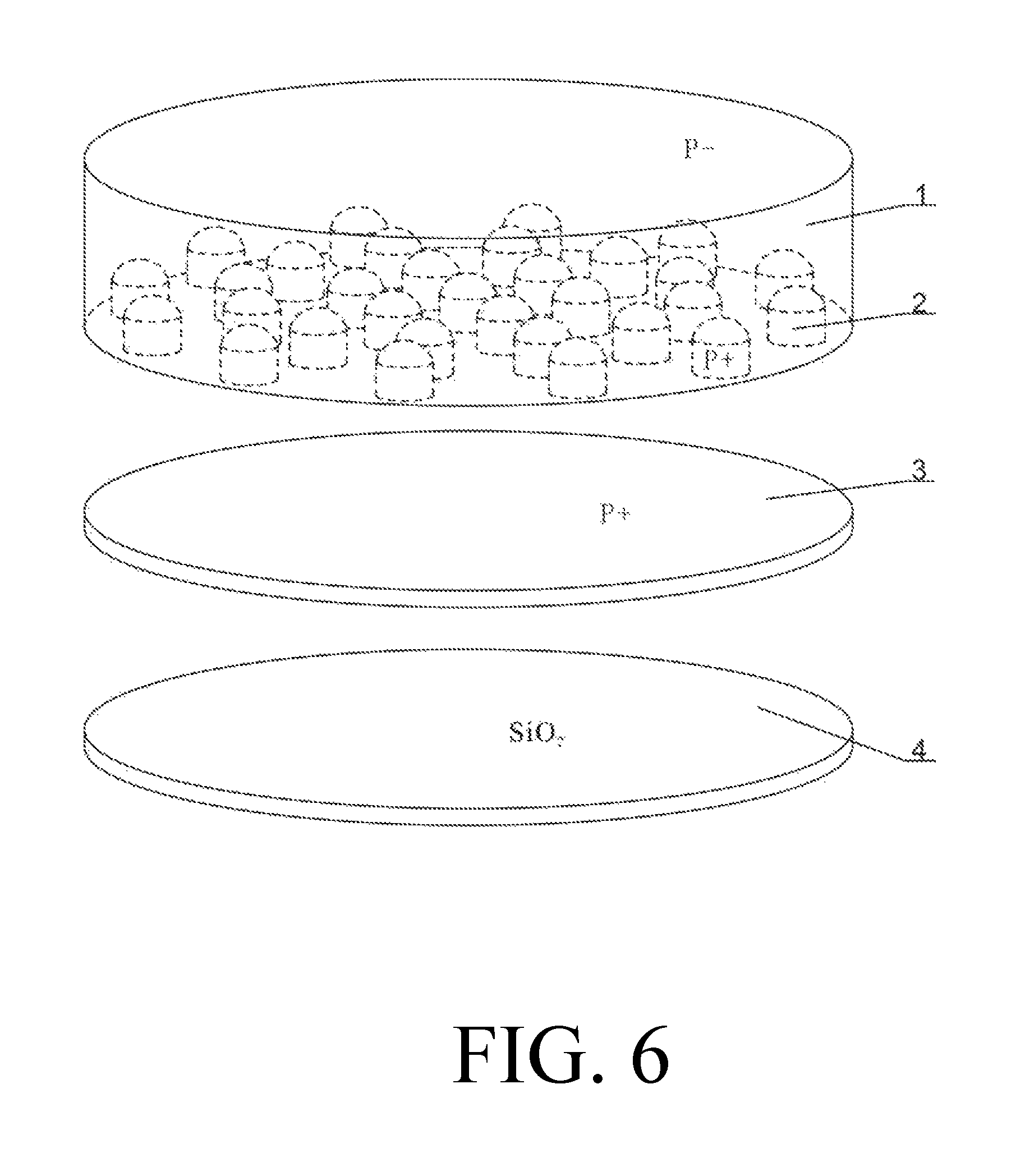
As shown in FIG. 6, the raw semiconductor wafer 1 is a lightly doped P-type region, namely a P.sup.- region; the connection layer is a heavily doped P-type region, namely a P.sup.+ region; for the array-distributed connection parts 2, the first ends are inserted into the raw semiconductor wafer 1, and the second ends are connected to each other on the bottom surface of the raw semiconductor wafer 1 through the conduction layer 3; the conduction layer 3 is a heavily doped P-type region, namely the P.sup.+ region; and the protection layer 4 is arranged on the conduction layer 3 at the bottom surface of the raw semiconductor wafer 1. The above three-dimensional semiconductor wafer is mainly applicable in production of P-channel enhancement mode MOSFET and giant transistor (GTR).
Sixth Preferred Embodiment
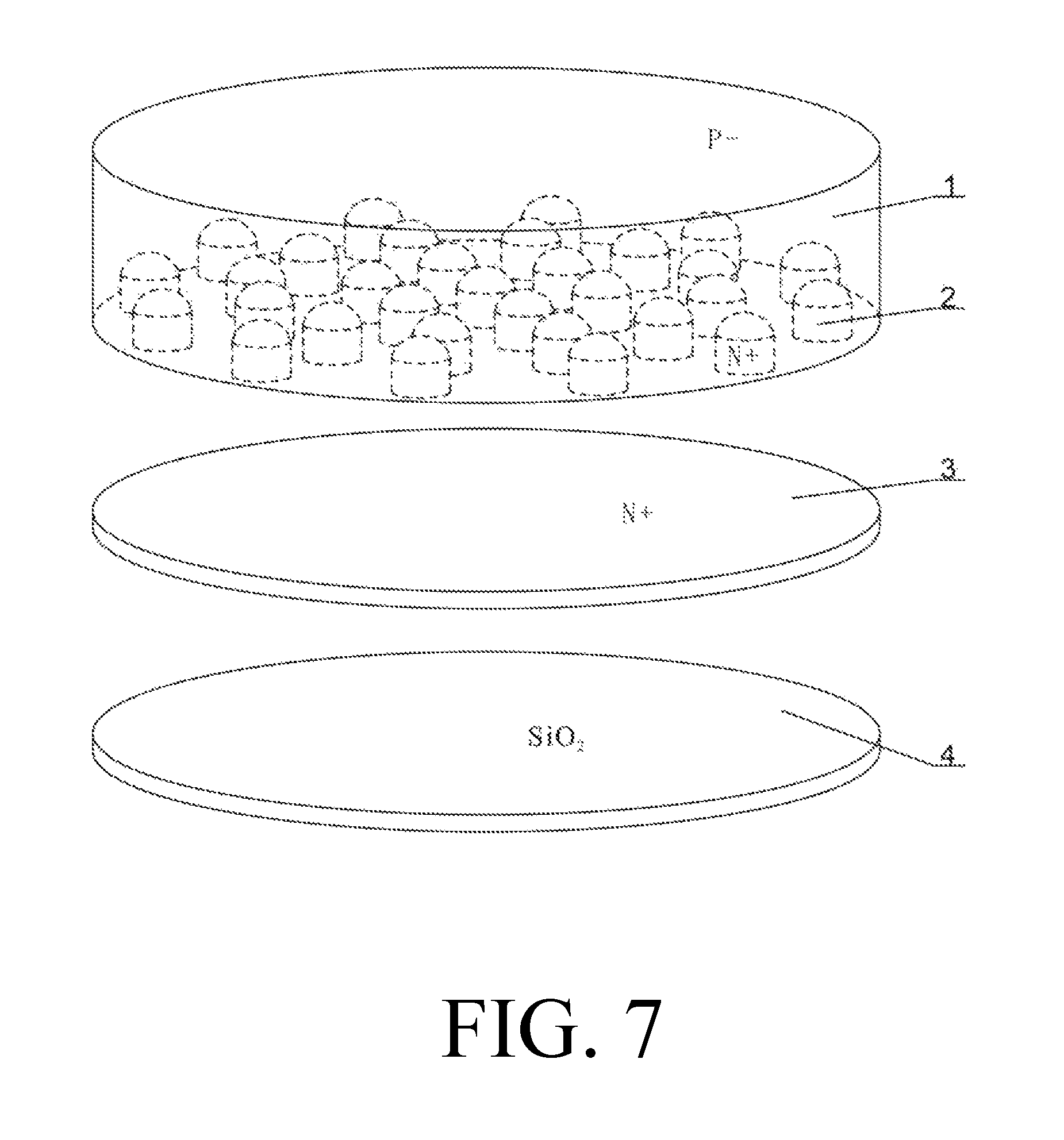
As shown in FIG. 7, the raw semiconductor wafer 1 is a lightly doped P-type region, namely a P.sup.- region; the connection layer is a heavily doped N-type region, namely an N.sup.+ region; for the array-distributed connection parts 2, the first ends are inserted into the raw semiconductor wafer 1, and the second ends are connected to each other on the bottom surface of the raw semiconductor wafer 1 through the conduction layer 3; the conduction layer 3 is a heavily doped N-type region, namely the N.sup.+ region; and the protection layer 4 is arranged on the conduction layer 3 at the bottom surface of the raw semiconductor wafer 1.
Seventh Preferred Embodiment
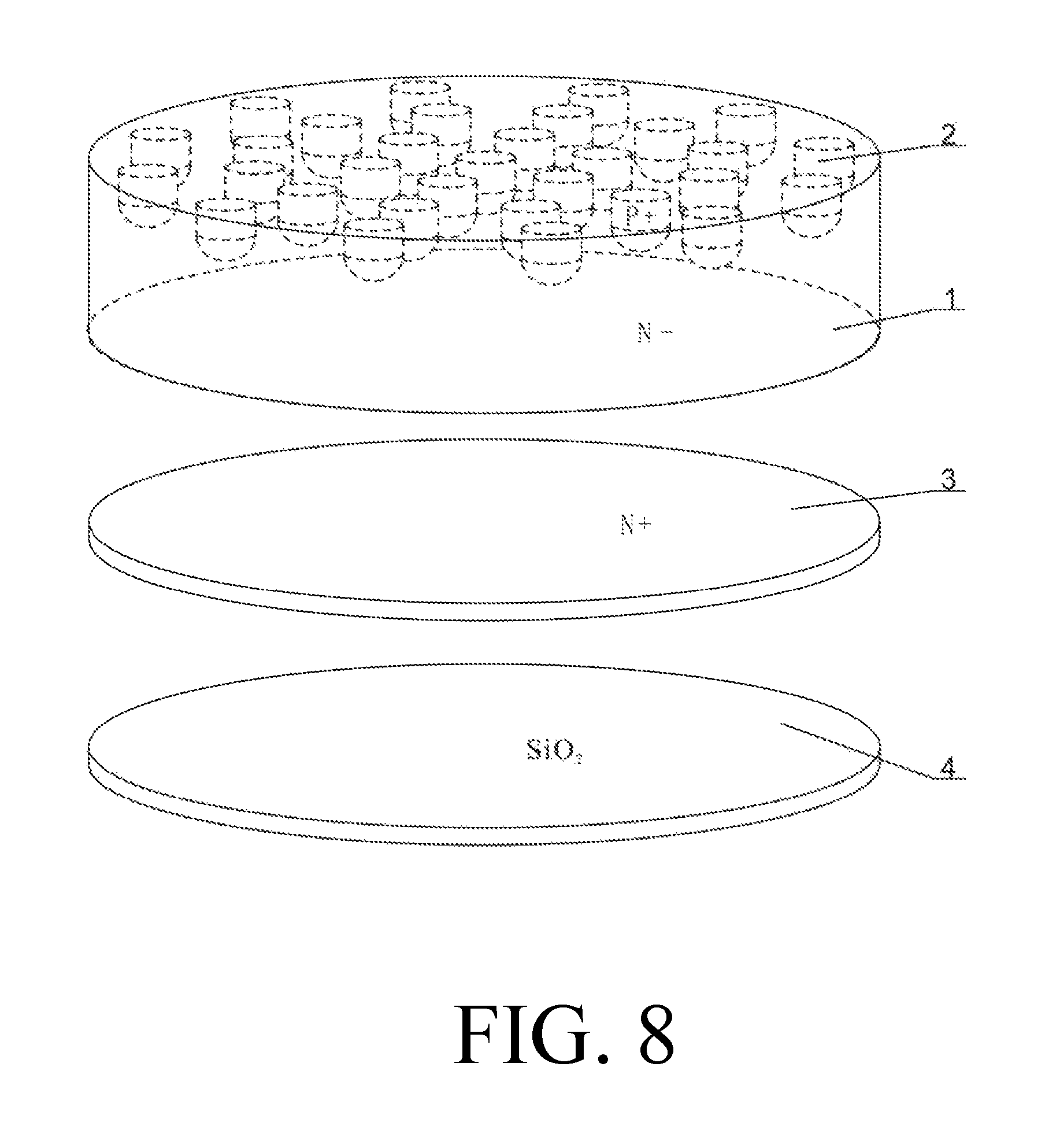
As shown in FIG. 8, the raw semiconductor wafer 1 is a lightly doped N-type region, namely an N.sup.- region; the connection layer is a heavily doped P-type region, namely a P.sup.+ region; for the array-distributed connection parts 2, the first ends are inserted into the raw semiconductor wafer 1, and the second ends are level with the top surface of the raw semiconductor wafer 1; the conduction layer 3 is a heavily doped N-type region, namely an N.sup.+ region; and the protection layer 4 is arranged on the conduction layer 3 at the bottom surface of the raw semiconductor wafer 1.
Eighth Preferred Embodiment
As shown in FIG. 9, the raw semiconductor wafer 1 is a lightly doped N-type region, namely an N.sup.- region; a first connection layer at the top surface of the raw semiconductor wafer is a heavily doped P-type region, namely a P.sup.+ region, and the array-distributed connection parts 2 of the first connection layer have the first ends inserted into the raw semiconductor wafer 1 and the second ends level with the top surface of the raw semiconductor wafer 1; a second connection layer at the bottom surface of the raw semiconductor wafer 1 is a heavily doped N-type region, namely an N.sup.+ region, and the array-distributed connection parts 2 of the second connection layer have the first ends inserted into the raw semiconductor wafer 1 and the second ends connected to each other on the bottom surface of the raw semiconductor wafer 1 through the conduction layer 3; the conduction layer 3 is a heavily doped N-type region, namely the N.sup.+ region; and the protection layer 4 is arranged on the conduction layer 3 at the bottom surface of the raw semiconductor wafer 1.
* * * * *
D00000
D00001
D00002
D00003
D00004
D00005
D00006
D00007
D00008
D00009
XML
uspto.report is an independent third-party trademark research tool that is not affiliated, endorsed, or sponsored by the United States Patent and Trademark Office (USPTO) or any other governmental organization. The information provided by uspto.report is based on publicly available data at the time of writing and is intended for informational purposes only.
While we strive to provide accurate and up-to-date information, we do not guarantee the accuracy, completeness, reliability, or suitability of the information displayed on this site. The use of this site is at your own risk. Any reliance you place on such information is therefore strictly at your own risk.
All official trademark data, including owner information, should be verified by visiting the official USPTO website at www.uspto.gov. This site is not intended to replace professional legal advice and should not be used as a substitute for consulting with a legal professional who is knowledgeable about trademark law.