Methods and apparatuses including command delay adjustment circuit
Ishibashi , et al.
U.S. patent number 10,290,336 [Application Number 15/595,056] was granted by the patent office on 2019-05-14 for methods and apparatuses including command delay adjustment circuit. This patent grant is currently assigned to Micron Technology, Inc.. The grantee listed for this patent is Micron Technology, Inc.. Invention is credited to Hiroki Fujisawa, Shuichi Ishibashi, Kazutaka Miyano.


| United States Patent | 10,290,336 |
| Ishibashi , et al. | May 14, 2019 |
Methods and apparatuses including command delay adjustment circuit
Abstract
Apparatuses for controlling latencies on input signal paths in semiconductor devices are disclosed. An example apparatus includes: a clock input buffer that provides a reference clock signal and a system clock signal based on an external clock signal; a command decoder that latches command signals with the system clock signal and further provides a signal based on the command signals; and a command delay adjustment circuit including: a clock synchronizing circuit that receives the signal, latches the signal with the system clock signal and provides a clock-synchronized read signal responsive to a shift cycle parameter.
| Inventors: | Ishibashi; Shuichi (Tachikawa, JP), Miyano; Kazutaka (Sagamihara, JP), Fujisawa; Hiroki (Sagamihara, JP) | ||||||||||
|---|---|---|---|---|---|---|---|---|---|---|---|
| Applicant: |
|
||||||||||
| Assignee: | Micron Technology, Inc. (Boise,
ID) |
||||||||||
| Family ID: | 60089689 | ||||||||||
| Appl. No.: | 15/595,056 | ||||||||||
| Filed: | May 15, 2017 |
Prior Publication Data
| Document Identifier | Publication Date | |
|---|---|---|
| US 20170309323 A1 | Oct 26, 2017 | |
Related U.S. Patent Documents
| Application Number | Filing Date | Patent Number | Issue Date | ||
|---|---|---|---|---|---|
| 15139102 | Apr 26, 2016 | 9865317 | |||
| Current U.S. Class: | 1/1 |
| Current CPC Class: | G11C 7/1015 (20130101); G11C 7/1087 (20130101); G11C 7/1093 (20130101); G11C 7/109 (20130101); G11C 29/023 (20130101); G11C 7/1057 (20130101); G11C 7/1084 (20130101); G11C 29/028 (20130101); G11C 7/222 (20130101); G11C 7/1069 (20130101); G11C 8/18 (20130101); G11C 8/10 (20130101); G11C 11/4076 (20130101); G11C 7/1096 (20130101); G11C 2207/2272 (20130101); G11C 2207/2254 (20130101); G11C 7/225 (20130101); G11C 7/1066 (20130101); G11C 7/22 (20130101); G11C 29/024 (20130101) |
| Current International Class: | G11C 11/4076 (20060101); G11C 8/10 (20060101); G11C 8/18 (20060101); G11C 7/10 (20060101); G11C 7/22 (20060101); G11C 29/02 (20060101) |
| Field of Search: | ;365/233.1,233.11,194,191 |
References Cited [Referenced By]
U.S. Patent Documents
| 4644248 | February 1987 | Brennen et al. |
| 5004933 | April 1991 | Widener |
| 5610558 | March 1997 | Mittel et al. |
| 5935253 | August 1999 | Conary et al. |
| 6111810 | August 2000 | Fujita |
| 6219384 | April 2001 | Kliza et al. |
| 6260128 | July 2001 | Ohshima et al. |
| 6275077 | August 2001 | Tobin et al. |
| 6292040 | September 2001 | Iwamoto et al. |
| 6327318 | December 2001 | Bhullar et al. |
| 6424592 | July 2002 | Maruyama |
| 6438055 | August 2002 | Taguchi et al. |
| 6459313 | October 2002 | Godbee et al. |
| 6489823 | December 2002 | Iwamoto |
| 6510095 | January 2003 | Matsuzaki et al. |
| 6636110 | October 2003 | Ooishi et al. |
| 6687185 | February 2004 | Keeth et al. |
| 6710726 | March 2004 | Kim et al. |
| 6744285 | June 2004 | Mangum et al. |
| 6759881 | July 2004 | Kizer et al. |
| 6781861 | August 2004 | Gomm et al. |
| 6839288 | January 2005 | Kim et al. |
| 6861901 | March 2005 | Prexl et al. |
| 6868504 | March 2005 | Lin |
| 6885252 | April 2005 | Hsu |
| 6914798 | July 2005 | Kwon et al. |
| 6930955 | August 2005 | Johnson et al. |
| 6973008 | December 2005 | Krause |
| 6980479 | December 2005 | Park |
| 6988218 | January 2006 | Drexler |
| 7042799 | May 2006 | Cho |
| 7046060 | May 2006 | Minzoni et al. |
| 7058799 | June 2006 | Johnson |
| 7061941 | June 2006 | Zheng |
| 7065001 | June 2006 | Johnson et al. |
| 7111185 | September 2006 | Gomm et al. |
| 7119591 | October 2006 | Lin |
| 7158443 | January 2007 | Lin |
| 7170819 | January 2007 | Szczypinski |
| 7187599 | March 2007 | Schnell et al. |
| 7209396 | April 2007 | Schnell |
| 7248512 | July 2007 | Shin |
| 7268605 | September 2007 | Fang et al. |
| 7269754 | September 2007 | Ramaswamy et al. |
| 7280430 | October 2007 | Lee |
| 7319728 | January 2008 | Bell et al. |
| 7336752 | February 2008 | Vlasenko et al. |
| 7340632 | March 2008 | Park |
| 7355464 | April 2008 | Lee |
| 7375560 | May 2008 | Lee et al. |
| 7411852 | August 2008 | Nishioka et al. |
| 7428284 | September 2008 | Lin |
| 7443216 | October 2008 | Gomm et al. |
| 7451338 | November 2008 | Lemos |
| 7463534 | December 2008 | Ku et al. |
| 7489172 | February 2009 | Kim |
| 7509517 | March 2009 | Matsumoto et al. |
| 7541851 | June 2009 | Gomm et al. |
| 7580321 | August 2009 | Fujisawa et al. |
| 7590013 | September 2009 | Yu et al. |
| 7593273 | September 2009 | Chu et al. |
| 7609584 | October 2009 | Kim et al. |
| 7616040 | November 2009 | Motomura |
| 7631248 | December 2009 | Zakharchenko et al. |
| 7643334 | January 2010 | Lee et al. |
| 7656745 | February 2010 | Kwak |
| 7660187 | February 2010 | Johnson et al. |
| 7663946 | February 2010 | Kim |
| 7671648 | March 2010 | Kwak |
| 7675439 | March 2010 | Chang et al. |
| 7675791 | March 2010 | Kim |
| 7698589 | April 2010 | Huang |
| 7715260 | May 2010 | Kuo et al. |
| 7716510 | May 2010 | Kwak |
| 7751261 | July 2010 | Cho |
| 7773435 | August 2010 | Cho |
| 7822904 | October 2010 | LaBerge |
| 7826305 | November 2010 | Fujisawa |
| 7826583 | November 2010 | Jeong et al. |
| 7872924 | January 2011 | Ma |
| 7876640 | January 2011 | Lin |
| 7885365 | February 2011 | Hagleitner et al. |
| 7913103 | March 2011 | Gold et al. |
| 7928782 | April 2011 | Booth et al. |
| 7945800 | May 2011 | Gomm et al. |
| 7948817 | May 2011 | Coteus et al. |
| 7969813 | June 2011 | Bringivijayaraghavan et al. |
| 7970090 | June 2011 | Tetzlaff |
| 7983094 | July 2011 | Roge et al. |
| 8004884 | August 2011 | Franceschini et al. |
| 8018791 | September 2011 | Kwak |
| 8030981 | October 2011 | Kim |
| 8115529 | February 2012 | Shibata |
| 8116415 | February 2012 | Wada et al. |
| 8144529 | March 2012 | Chuang et al. |
| 8321714 | November 2012 | Wu et al. |
| 8358546 | January 2013 | Kim et al. |
| 8392741 | March 2013 | Kim et al. |
| 8441888 | May 2013 | Bringivijayaraghavan et al. |
| 8509011 | August 2013 | Bringivijayaraghavan |
| 8536915 | September 2013 | Terrovitis |
| 8644096 | February 2014 | Bringivijayaraghavan |
| 8717078 | May 2014 | Idgunji et al. |
| 8732509 | May 2014 | Kwak |
| 8788896 | July 2014 | Tekumalla |
| 9001955 | April 2015 | Lamanna et al. |
| 9053815 | June 2015 | Bell |
| 9054675 | June 2015 | Mazumder et al. |
| 9166579 | October 2015 | Huber et al. |
| 9329623 | May 2016 | Vankayala |
| 9508409 | November 2016 | Kwak |
| 9529379 | December 2016 | Kwak |
| 9530473 | December 2016 | Mazumder |
| 9531363 | December 2016 | Miyano |
| 9601170 | March 2017 | Mazumder et al. |
| 9865317 | January 2018 | Ishibashi et al. |
| 10193558 | January 2019 | Ma et al. |
| 2001/0015924 | August 2001 | Arimoto et al. |
| 2002/0057624 | May 2002 | Manning |
| 2002/0110035 | August 2002 | Li et al. |
| 2002/0149506 | October 2002 | Altrichter et al. |
| 2003/0117864 | June 2003 | Hampel et al. |
| 2003/0147299 | August 2003 | Setogawa |
| 2003/0161210 | August 2003 | Acharya et al. |
| 2004/0000934 | January 2004 | Jeon |
| 2004/0008064 | January 2004 | Kashiwazaki |
| 2004/0041604 | March 2004 | Kizer et al. |
| 2005/0017774 | January 2005 | Chow et al. |
| 2005/0024107 | February 2005 | Takai et al. |
| 2005/0047222 | March 2005 | Rentschler |
| 2005/0052309 | March 2005 | Wang |
| 2005/0132043 | June 2005 | Wang et al. |
| 2005/0184780 | August 2005 | Chun |
| 2005/0270852 | December 2005 | Dietrich et al. |
| 2006/0033542 | February 2006 | Lin et al. |
| 2006/0055441 | March 2006 | McClannahan et al. |
| 2006/0062341 | March 2006 | Edmondson et al. |
| 2006/0064620 | March 2006 | Kuhn et al. |
| 2006/0155948 | July 2006 | Ruckerbauer |
| 2006/0182212 | August 2006 | Hwang et al. |
| 2006/0193194 | August 2006 | Schnell |
| 2006/0250861 | November 2006 | Park et al. |
| 2006/0250883 | November 2006 | Szczypinski |
| 2007/0033427 | February 2007 | Correale, Jr. et al. |
| 2007/0046346 | March 2007 | Minzoni |
| 2007/0086267 | April 2007 | Kwak |
| 2007/0088903 | April 2007 | Choi |
| 2007/0192651 | August 2007 | Schoch |
| 2007/0291558 | December 2007 | Joo |
| 2008/0042705 | February 2008 | Kim et al. |
| 2008/0080267 | April 2008 | Lee |
| 2008/0080271 | April 2008 | Kim |
| 2008/0082707 | April 2008 | Gupta et al. |
| 2008/0126822 | May 2008 | Kim et al. |
| 2008/0137471 | June 2008 | Schnell et al. |
| 2008/0144423 | June 2008 | Kwak |
| 2008/0180144 | July 2008 | Mai |
| 2008/0204071 | August 2008 | Lee et al. |
| 2008/0232179 | September 2008 | Kwak |
| 2008/0232180 | September 2008 | Kim et al. |
| 2008/0253205 | October 2008 | Park |
| 2009/0041104 | February 2009 | Bogdan |
| 2009/0219068 | September 2009 | Mizuhashi et al. |
| 2009/0232250 | September 2009 | Yamada et al. |
| 2009/0290445 | November 2009 | Kinoshita et al. |
| 2009/0315600 | December 2009 | Becker et al. |
| 2010/0001762 | January 2010 | Kim |
| 2010/0052739 | March 2010 | Shibata |
| 2010/0054060 | March 2010 | Ku |
| 2010/0058261 | March 2010 | Markov et al. |
| 2010/0066422 | March 2010 | Tsai |
| 2010/0124090 | May 2010 | Arai |
| 2010/0124102 | May 2010 | Lee et al. |
| 2010/0128543 | May 2010 | Kwon et al. |
| 2010/0142308 | June 2010 | Kim |
| 2010/0165769 | July 2010 | Kuroki |
| 2010/0165780 | July 2010 | Bains et al. |
| 2010/0177589 | July 2010 | Kinoshita |
| 2010/0195429 | August 2010 | Sonoda |
| 2010/0199117 | August 2010 | Kwak |
| 2010/0208534 | August 2010 | Fujisawa |
| 2010/0208535 | August 2010 | Fujisawa |
| 2010/0232213 | September 2010 | Hwang et al. |
| 2010/0254198 | October 2010 | Bringivijayaraghavan et al. |
| 2010/0295584 | November 2010 | Sano |
| 2010/0327926 | December 2010 | Takahashi |
| 2011/0026318 | February 2011 | Franceschini et al. |
| 2011/0047319 | February 2011 | Jeon et al. |
| 2011/0055671 | March 2011 | Kim et al. |
| 2011/0057697 | March 2011 | Miyano |
| 2011/0058437 | March 2011 | Miyano |
| 2011/0102039 | May 2011 | Shin |
| 2011/0194575 | August 2011 | Chen et al. |
| 2011/0228625 | September 2011 | Bringivijayaraghavan |
| 2011/0238866 | September 2011 | Zitlaw |
| 2011/0238941 | September 2011 | Xu et al. |
| 2011/0298505 | December 2011 | Khoury et al. |
| 2011/0298512 | December 2011 | Kwak |
| 2011/0304365 | December 2011 | Bunch |
| 2012/0084575 | April 2012 | Flores et al. |
| 2012/0124317 | May 2012 | Mirichigni et al. |
| 2012/0147692 | June 2012 | Nakamura et al. |
| 2012/0212268 | August 2012 | Kim |
| 2012/0254873 | October 2012 | Bringivijayaraghavan |
| 2012/0269015 | October 2012 | Bringivijayaraghavan |
| 2012/0274376 | November 2012 | Gomm et al. |
| 2013/0002318 | January 2013 | Lu et al. |
| 2013/0002320 | January 2013 | Lin et al. |
| 2013/0141994 | June 2013 | Ito et al. |
| 2013/0194013 | August 2013 | Kwak et al. |
| 2013/0250701 | September 2013 | Bringivijayaraghavan et al. |
| 2013/0321052 | December 2013 | Huber et al. |
| 2013/0329503 | December 2013 | Bringivijayaraghavan |
| 2013/0342254 | December 2013 | Mazumder et al. |
| 2014/0010025 | January 2014 | Bringivijayaraghavan |
| 2014/0035640 | February 2014 | Kwak et al. |
| 2014/0055184 | February 2014 | Vankayala |
| 2014/0119141 | May 2014 | Tamlyn et al. |
| 2014/0176213 | June 2014 | Rylov |
| 2014/0177359 | June 2014 | Kumar et al. |
| 2014/0177361 | June 2014 | Kitagawa |
| 2014/0258764 | September 2014 | Kwak |
| 2014/0293719 | October 2014 | Jung |
| 2014/0340158 | November 2014 | Thandri et al. |
| 2015/0097604 | April 2015 | Taniguchi |
| 2015/0156009 | June 2015 | Bogdan |
| 2015/0170725 | June 2015 | Kwak |
| 2015/0235691 | August 2015 | Kwak |
| 2015/0263739 | September 2015 | Jung et al. |
| 2015/0263740 | September 2015 | Jung et al. |
| 2015/0340072 | November 2015 | Mazumder |
| 2016/0013799 | January 2016 | Li et al. |
| 2016/0056807 | February 2016 | Neidengard et al. |
| 2016/0322964 | November 2016 | Miyano |
| 2016/0365860 | December 2016 | Ma et al. |
| 2017/0288682 | October 2017 | Ma et al. |
| 2017/0309320 | October 2017 | Ishibashi et al. |
| 2018/0053538 | February 2018 | Miyano et al. |
| 2018/0286470 | October 2018 | Miyano et al. |
| 2018/0358064 | December 2018 | Ishibashi et al. |
| 1952868 | Apr 2007 | CN | |||
| 101752009 | Jun 2010 | CN | |||
| 2013-222997 | Oct 2013 | JP | |||
| 201303735 | Jan 2013 | TW | |||
| 2017189127 | Nov 2017 | WO | |||
| 2018038835 | Mar 2018 | WO | |||
Other References
|
International Search Report and Written Opinion dated Jun. 27, 2017 for PCT application No. PCT/US2017/023594; pp. all. cited by applicant . U.S. Appl. No. 15/243,651, entitled "Apparatuses and Methods for Adjusting Delay of Command Signal Path", filed Aug. 22, 2016. cited by applicant . "Interfacing DDR SDRAM with Stratix II Devices", Version 3.2, Altera Corp, Sep. 2008. cited by applicant . Lee, "How to implement DDR SGRAM in Graphic System", Samsung Electric, 4Q1998 (Oct.-Dec. 1998). cited by applicant . U.S. Appl. No. 16/286,829, titled "Apparatuses and Methods for Indirectly Detecting Phase Variations" filed Feb. 27, 2019, pp. all. cited by applicant. |
Primary Examiner: Pham; Ly D
Attorney, Agent or Firm: Dorsey & Whitney LLP
Parent Case Text
CROSS-REFERENCE TO RELATED APPLICATIONS
This application is a continuation of U.S. application Ser. No. 15/139,102, filed Apr. 26, 2016, issued as U.S. Pat. No. 9,865,317 on Jan. 9, 2018. The afore-mentioned application and patent are incorporated herein by reference, in their entirety, for any purpose.
Claims
What is claimed is:
1. An apparatus comprising: a first circuit configured to respond to a first clock signal to latch a first signal, the first circuit being configured to provide a second signal; a second circuit coupled to the first circuit to latch the second signal, the second circuit being configured to provide a third signal based on the second signal in response to a first output timing signal that is substantially in phase to the first clock signal; and a clock input buffer circuit configured to generate the first clock signal in response to an enable signal, wherein the first circuit is coupled to the clock input buffer circuit and further configured to provide the enable signal to the clock input buffer.
2. The apparatus as claimed in claim 1, wherein the first circuit is configured to decode the first signal to provide the second signal.
3. The apparatus as claimed in claim 2, wherein the first circuit is a command decoder circuit and the first signal includes a command signal.
4. The apparatus as claimed in claim 1, further comprising: a first delay circuit configured to receive a second clock signal that is substantially in phase to the first clock signal and further configured to provide a third clock signal by delaying the second clock signal by a first delay that is adjustable; a second delay circuit coupled to the second circuit and configured to provide a fourth signal by delaying the third signal by a second delay that is adjustable; and a delay control circuit configured to adjust the first delay of the first circuit and the second delay of the second delay circuit to be substantially equal to each other.
5. The apparatus as claimed in claim 4, further comprising: a third circuit coupled to the second delay circuit and configured to provide a fifth signal by delaying the fourth signal in response to the third clock signal and latency information; and an output buffer coupled to the third circuit and configured to be activated in response to the fifth signal and further configured to operate in response to the third clock signal.
6. The apparatus as claimed in claim 1, wherein the second circuit is further configured to latch the second signal in response to a first input signal that is delayed in phase from the first clock signal.
7. The apparatus as claimed in claim 6, wherein the second circuit further comprises: a counter circuit configured to receive the first clock signal and further configured to provide a plurality of timing control signals in response to the first clock signal; a third delay circuit coupled to the counter circuit and configured to provide a plurality of second input timing signals by delaying the timing control signals; a first decoder coupled to the third delay circuit and configured to provide a first input timing signal by decoding the second input timing signals; and a second decoder coupled to the counter circuit and configured to provide the first output timing signal by decoding the timing control signals.
8. The apparatus as claimed in claim 7, wherein the third delay circuit is configured to represent a first delay that is substantially constant.
9. The apparatus as claimed in claim 7, wherein the first decoder is further configured to provide a third input timing signal by decoding the second input timing signals, wherein the second decoder is further configured to provide a second output timing signal by decoding the timing control signals, and wherein the second circuit further comprises: first and second input latch circuits coupled in common to the first circuit and configured to latch the second signal in response to the first input timing signal and the second input timing signal, respectively; first and second output latch circuits coupled to the first and second input latch circuit and configured to output the third signal in response to the first output timing signal and the second output timing signal, respectively; and a selector circuit including first and second input nodes coupled respectively to the first and second input latch circuits and first and second output nodes coupled respectively to the first and second output latch circuits, the selector circuit being configured to couple the first and second input latch circuits to the first and second output latch circuit in response to a selector control signal.
10. The apparatus as claimed in claim 9, further comprising: a third circuit coupled to the second circuit and configured to provide the selector control signal in response to a latency information.
11. A method comprising: providing a system clock signal; latching command signals respective to the system clock signal; providing a signal based on the command signals; latching the signal responsive to the system clock signal; and providing a clock-synchronized read signal responsive to latency information, wherein the latency information used to provide the clock-synchronized read signal is a latency between the system clock signal and the clock-synchronized read signal, and the clock-synchronized read signal is provided based on both the command signals and the signal latched responsive to the system clock signal.
12. The method of claim 11, wherein the system clock signal is based on an external clock signal.
13. The method of claim 11, wherein the clock synchronized read signal is responsive to a shift cycle parameter responsive to the latency information.
14. The method of claim 11, wherein latching command signals responsive to the system clock signal comprises: latching the command signals responsive a first clock signal responsive to the system clock signal; providing a read signal or a write signal as an output signal responsive to a read command or a write command on the command signals; latching the read signal or the write signal responsive to a second clock signal responsive to the first clock signal; providing the latched read signal or the latched write signal as an internal signal; latching the internal signal responsive to the second clock signal; and providing an enable signal responsive to the latched internal signal.
15. The method of claim 14, wherein the providing the system clock signal comprises: providing a reference clock signal responsive to the enable signal.
16. The method of claim 15, wherein providing the system clock signal comprises: providing the reference clock signal and the system clock signal based on an external clock signal.
17. The method of claim 11, wherein latching the signal responsive to the system clock signal comprises: receiving the system clock signal; providing a plurality of first timing control signals responsive to the system clock signal, providing a plurality of second timing control signals that has a predetermined delay from the system clock signal; and providing pointer input signals by decoding the plurality of second timing control signals, and wherein providing the clock-synchronized read signal responsive to the latency information comprises: receiving the system clock signal and the plurality of first timing control signals; and providing pointer output signals by decoding the plurality of first timing control signals responsive to the system clock signal.
Description
BACKGROUND
High data reliability, high speed of memory access, and low power consumption are features that are demanded from semiconductor memory. In recent years, there has been an effort to further increase the speed of memory access. Many synchronous integrated circuits in a semiconductor device perform operations based on a clock signal to meet critical timing requirements.
In order to assess performance of a pulse-signal transmission system, a window or "data eye" pattern may be evaluated. The data eye for each of the data signals defines the actual duration that each signal is valid after various factors affecting the signal are considered, such as timing skew, voltage and current drive capability, for example. In the case of timing skew of signals, it often arises from a variety of timing errors such as loading on the lines of the bus and the physical lengths of such lines. For example, a rank margining test (RMT) may be used to evaluate the window in order to assess performance tolerance of an input buffer in a semiconductor device. In the RMT, a reference voltage (VREF) level may be varied from a mid-point between a voltage of input high (VIH) and a voltage of input low (VIL) to test a margin of RMT as performance tolerance. The input buffer is required to operate without any errors even if the reference voltage shifts, as long as the reference voltage is in a predetermined range.
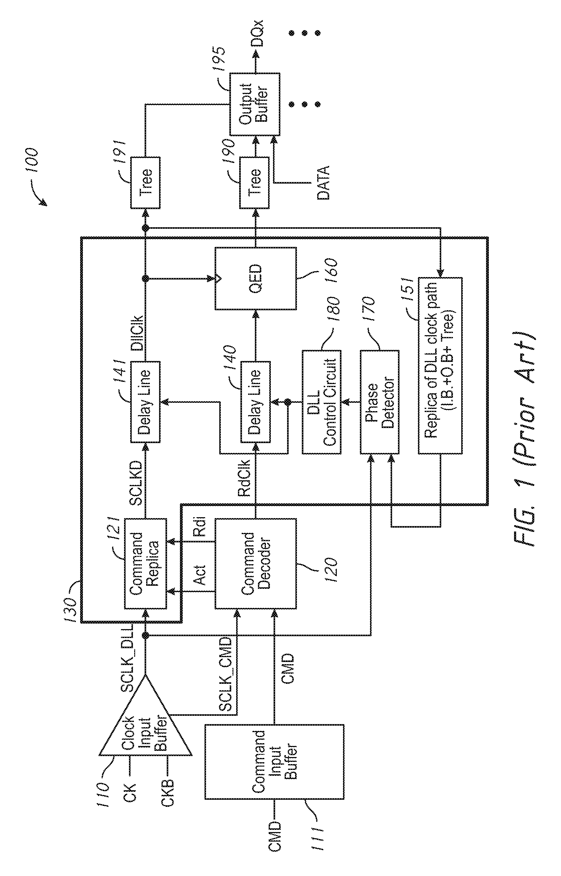
FIG. 1 is a block diagram of an apparatus 100 including a command delay adjustment circuit 130. The apparatus 100 may include a clock input buffer 110, a command input buffer 111, a command decoder circuit 120, the command delay adjustment circuit 130, signal trees 190 and 191 for a command signal and a clock signal, and an output buffer 195.
The command delay adjustment circuit 130 may include a DLL clock path and a command path. The DLL clock path may include a command replica 121, and a delay line 141 for the clock signal. The command replica 121 replicates a delay of the command decoder circuit 120 in providing an RdClk signal responsive to command signals CMD and a system clock signal SCLK_CMD signals. The command replica 121 may delay a SCLK_DLL signal and provide a delayed system clock signal SCLKD to the delay line 141. The command path includes a delay line 140 for the command signal and a dQ-Enable-Delay (QED) circuit 160. The command delay adjustment circuit 130 further includes a replica of the DLL clock path 151, a phase detector 170 and a DLL control circuit 180 which form a DLL circuit together with the delay line 141 for the clock signal.
The command delay adjustment circuit 130 may synchronize an output signal of the dQ-Enable-Delay circuit 160 with a DLL clock signal DllClk from the delay line 141 while providing a latency on the output signal of the dQ-Enable-Delay circuit 160. The latency here is, for example, a column address strobe (CAS) latency (CL), which may be set based on a clock frequency of the clock signal CK. The CL value may account for a delay time between when a memory receives a READ command and when the output buffer 195 provides read data responsive to the READ command to an output bus (e.g., via a DQ pad after the output buffer 195). The CL value may be represented as a number of clock cycles. One clock cycle can be represented by T.
However, there are side effects that increase jitter of the SCLKD signal from the command replica 121, and increased active standby current (e.g., IDD3N). In turn, the jitter in the SCLKD signal increases jitter of the DLL clock signal DllClk, which causes the decrease of the margin of RMT. Thus, higher speed of memory access enabled by adding the command replica 121 may cause a decrease in the margin of RMT, accompanied with higher power consumption.
BRIEF DESCRIPTION OF THE DRAWINGS
FIG. 1 is a block diagram of an apparatus including a command delay adjustment circuit in read operation.
FIG. 2 is a block diagram of an apparatus including a command delay adjustment circuit in accordance with an embodiment of the present disclosure.
FIG. 3 is a block diagram of a clock synchronizing circuit in accordance with an embodiment of the present disclosure.
FIG. 4A is a diagram of cells of an input pointer register in a clock synchronizing circuit in accordance with an embodiment of the present disclosure.
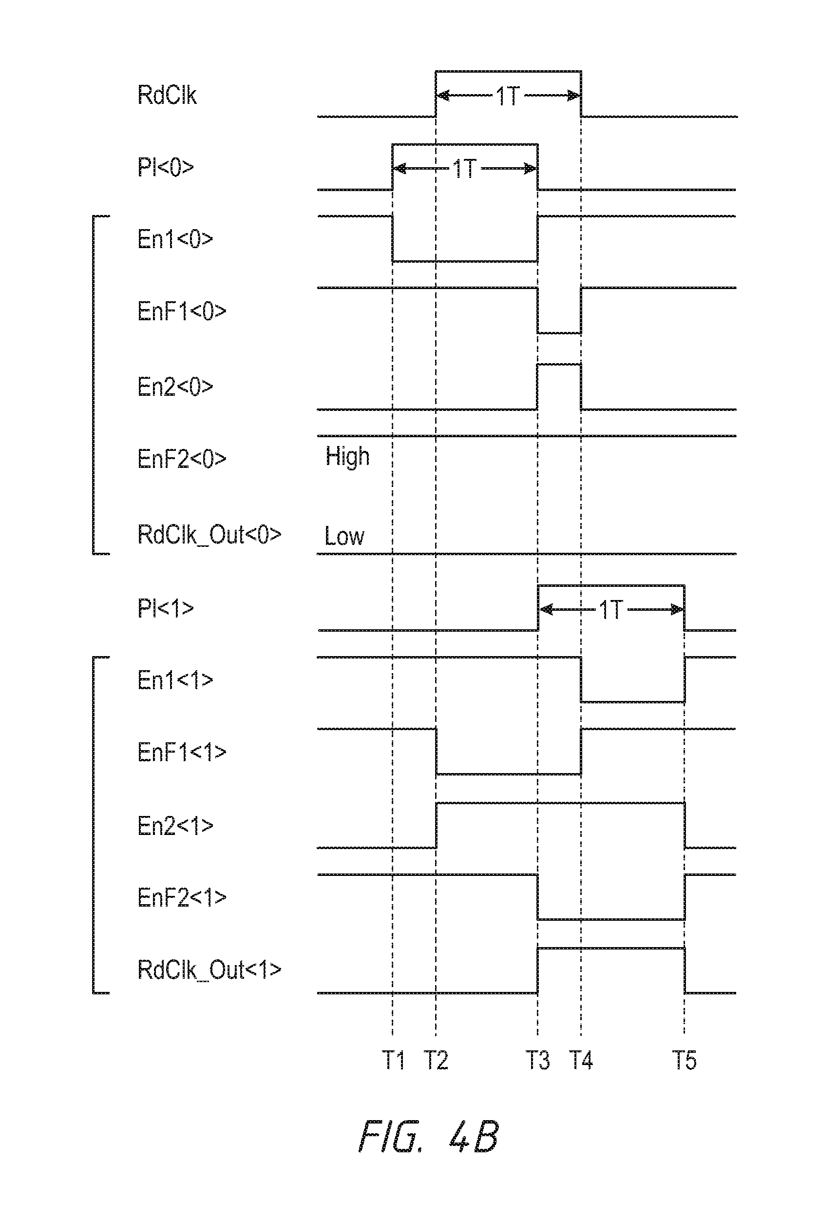
FIG. 4B is a timing diagram of signals in cells of the input pointer register of FIG. 4A, in accordance with an embodiment of the present disclosure.
FIG. 5 is a circuit diagram of a command decoder circuit in an apparatus including a command delay adjustment circuit, in accordance with an embodiment of the present disclosure.
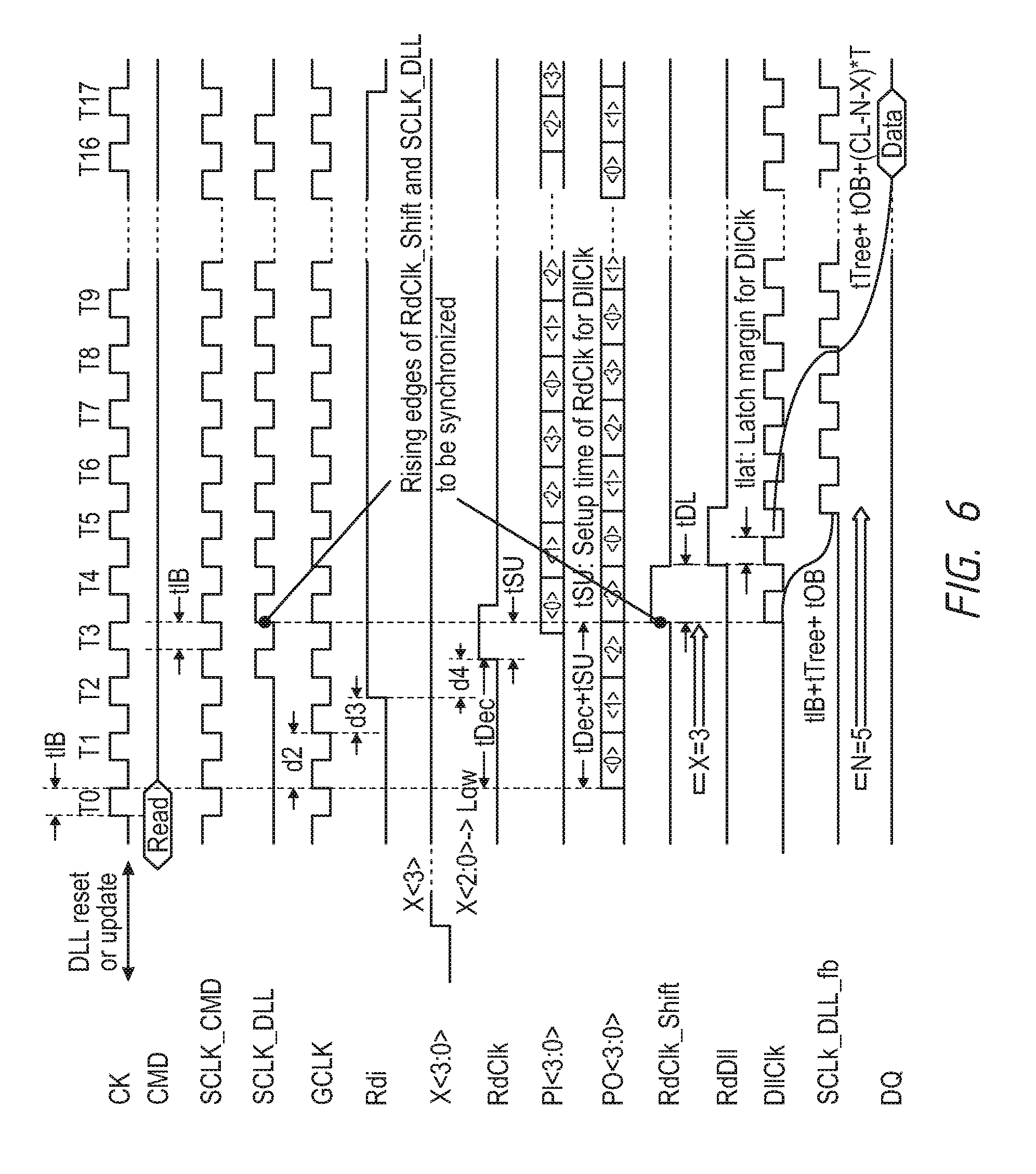
FIG. 6 is a timing diagram of signals in an apparatus including a command delay adjustment circuit, in accordance with an embodiment of the present disclosure.
DETAILED DESCRIPTION OF PREFERRED EMBODIMENTS
Various embodiments of the present disclosure will be explained below in detail with reference to the accompanying drawings. The following detailed description refers to the accompanying drawings that show, by way of illustration, specific aspects and embodiments in which the present invention may be practiced. These embodiments are described in sufficient detail to enable those skilled in the art to practice the present invention. Other embodiments may be utilized, and structure, logical and electrical changes may be made without departing from the scope of the present invention. The various embodiments disclosed herein are not necessary mutually exclusive, as some disclosed embodiments can be combined with one or more other disclosed embodiments to form new embodiments.
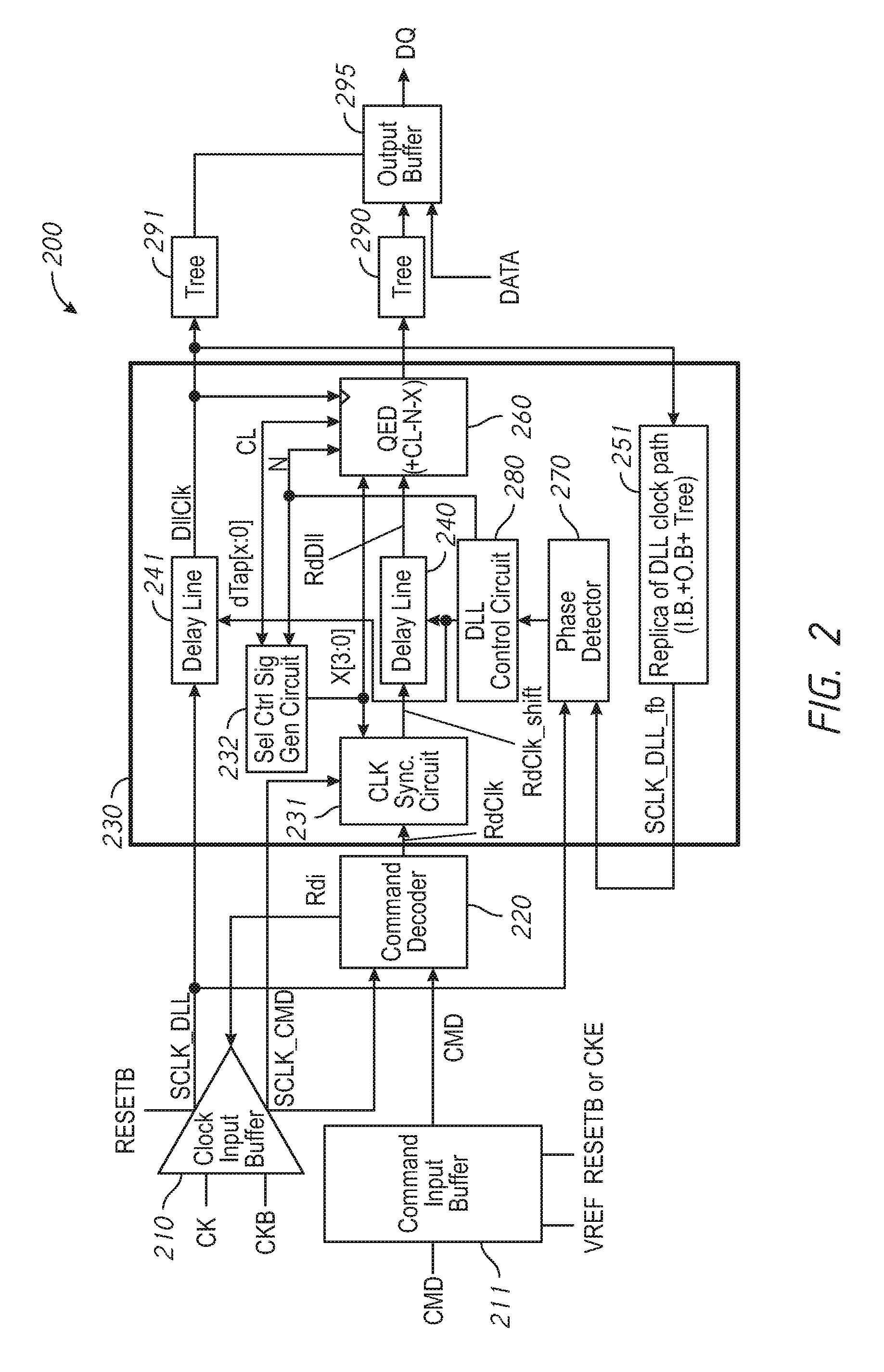
FIG. 2 is a block diagram of an apparatus 200 including a command delay adjustment circuit 230 in accordance with an embodiment of the present disclosure. The apparatus 200 may include a clock input buffer 210, a command input buffer 211, a first circuit 220 (which may also be referred to herein as a command decoder circuit), the command delay adjustment circuit 230, signal trees 290 and 291 for a command signal and a clock signal and an output buffer 295. The clock input buffer 210 receives a clock signal CK, a complementary clock signal CKB both of which are external clock signals, and further receives a complementary reset signal RESETB. The clock input buffer 210 further receives an enable signal Rdi based on a READ command from the command decoder circuit 220. The clock input buffer 210 may provide a system clock signal SCLK_CMD and a reference clock signal SCLK_DLL responsive, at least in part, to the clock signal CK and a complementary clock signal CKB. The system clock signal SCLK_CMD and the reference clock signal SCLK_DLL may be synchronized with each other or be in phase to each other. The clock input buffer 210 may enable or disable providing the reference clock signal SCLK_DLL, at least partly responsive to the enable signal Rdi. The command input buffer 211 receives a first signal (which may also be referred to herein as a command signal CMD), a reference voltage VREF and either the complementary signal RESETB or a clock enable signal CKE. The command input buffer 211 provides the command signal CMD to the command decoder circuit 220. The command decoder circuit 220 receives the system clock signal SCLK_CMD and the command signal CMD. The command decoder circuit 220 decodes the commands on the command signal CMD, responsive to the system clock signal SCLK_CMD to provide a pulse on a second signal (which may also be referred to herein as a command delay line input signal RdClk). As earlier described, the command decoder circuit 220 may provide the enable signal Rdi responsive to a command signal for a READ operation.
The command delay adjustment circuit 230 may include a DLL clock path and a command path. The DLL clock path may include a delay line circuit 241 for the clock signal. The command path includes a second circuit 231 (which may also be referred to herein as a clock synchronizing circuit), a delay line circuit 240 for the command signal and a third circuit 260 (which may also be referred to herein as a QED circuit). The command delay adjustment circuit 230 further includes a selector control signal generator circuit 232, a replica of the DLL clock path 251, a phase detector 270 and a delay control circuit 280 (which may also be referred to herein as a DLL control circuit). The replica of the DLL clock path 251, the phase detector 270 and the DLL, control circuit 280 form a DLL circuit together with the delay line 241 for the clock signal. The clock synchronizing circuit 231 receives a command delay line input signal RdClk from the command decoder circuit 220, the system clock signal SCLK_CMD from the dock input buffer 210, and a shift cycle parameter X (X[3:0]) from the selector control signal generator circuit 232. The clock synchronizing circuit 231 is provided to absorb a time lag tDec due to command decoding and latching in the command decoder circuit 220. The clock synchronizing circuit 231 synchronizes rising edges of the command delay line input signal RdClk with rising edges of the system clock signal SCLK_CMD, and provides a third signal (which may also be referred to herein as a clock-synchronized read signal RdClk_shift). The selector control signal generator circuit 232 may provide the shift cycle parameter X (X[3:0]) to the clock synchronizing circuit 231 and the QED circuit 260. The shift cycle parameter X represents a number of clock cycles to shift (e.g., maximum three clock cycles in this embodiment) for absorbing the time lag tDec. In some embodiment, the shift cycle parameter X may represent more than three clock cycles. The selector control signal generator circuit 232 receives an N value that may be described later in detail from the DLL control circuit 280 and a predetermined CL value which may be frequency dependent value, and provides the shift cycle parameter X (X[3:0]) in a DLL reset sequence or in a DLL update sequence by assigning an extra period "CL-N" to X with a subtractor.
The delay lines 240 and 241 include adjustable delay circuits. The delay line 240 receives the clock-synchronized read signal RdClk-shift and a tap signal (dTap[x:0]) from the DLL control circuit 280 and provides a fourth signal (which may also be referred to herein as a delayed read signal RdDll). The DLL control circuit 280 further provides the N value which represents a timing relationship between the reference clock signal SCLK_DLL and a feedback clock signal SCLK_DLL_fb, that may be a number of clock cycles to achieve a locked condition in which the reference clock signal SCLK_DLL and the feedback clock signal SCLK_DLL_fb are in phase to each other. The N value may be provided to the selector control signal generator circuit 232 and the QED circuit 260 after reaching the locked condition. The QED circuit 260 synchronizes the delayed read signal RdDll from the delay line 240 with the DLL clock signal DllClk from the delay line 241. The QED circuit 260 adjusts a latency of the delayed read signal RdDll using the N value and the CL value as well as the shift cycle parameter X. The QED circuit 260 provides a fifth signal (which may also be referred to herein as a read activation signal).
The phase detector 270 detects a phase difference between the feedback clock signal SCLK_DLL_fb through the model delays and the reference signal SCLK_DLL and provide the detected phase difference to the DLL control circuit 280. Based on the phase difference between the reference signal SCLK_DLL and the feedback clock signal SCLK_DLL_fb, the DLL control circuit 280 may adjust the delays of the delay lines 240 and 241 so that rising edges of the feedback clock signal SCLK_DLL_fb and rising edges of the reference clock signal SCLK_DLL are synchronized. The DLL control circuit 280 controls the delay lines 240 and 241 to have substantially the same delay. To provide a latch margin between the DLL clock signal DllClk from the delay line 241 and the delayed read signal RdDll in the QED circuit 260, the rising edges of the reference clock SCLK_DLL and rising edges of the clock-synchronized read signal RdClk_shift are controlled to synchronize before the delay line 240. By including the clock synchronizing circuit 231, the two delay lines 240 and 241 can use an identical tap signal dTap[x:0] to have the same delay. Thus, the rising edge timings of the reference clock signal SCLK_DLL and the rising edges of the clock-synchronized read signal RdCll_shift can be synchronized by adding the clock synchronizing circuit 231 on the command path for data transmission.
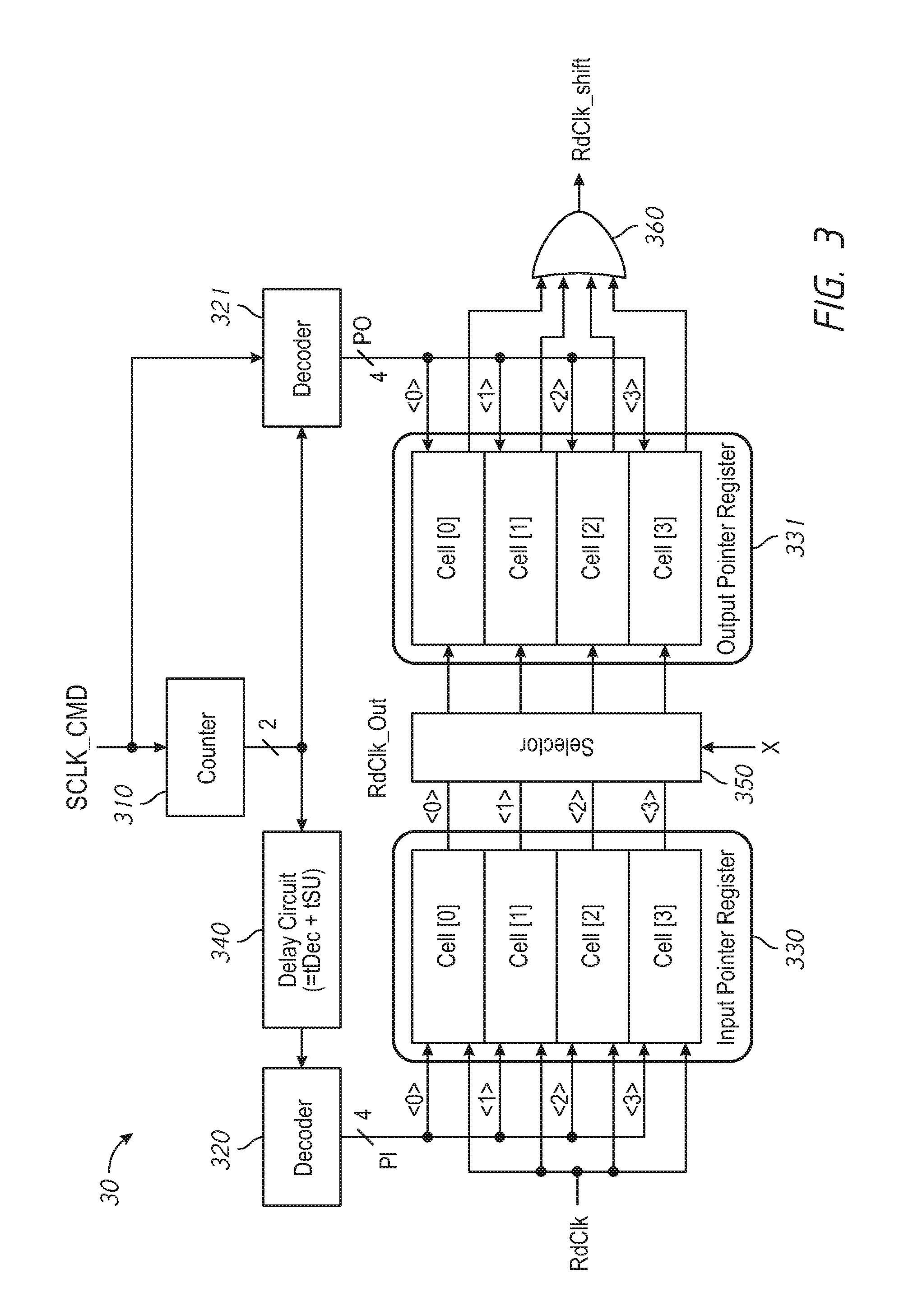
FIG. 3 is a block diagram of a clock synchronizing circuit in accordance with an embodiment of the present disclosure. For example, the clock synchronizing circuit 30 may be the clock synchronizing circuit 231 on the command path in FIG. 2. The clock synchronizing circuit 30 is a first-in-first-out (FIFO) circuit which receives a command delay line input signal RdClk, a system clock signal SCLK_CMD, and a shift cycle parameter X (X[3:0]). The clock synchronizing circuit 30 includes a counter circuit 310, a plurality of decoder circuits 320 and 321, an input pointer register 330 including a plurality of cells and an output pointer register 331 including a plurality of cells. The plurality of decoders 320 and 321 may be four-bit decoders. A FIFO clock signal may be generated by using the counter circuit 310. In some embodiments, the counter circuit 310 may be a Gray code counter, however, in other embodiments other types of counters may be used as the counter circuit 310. In this embodiment, the counter circuit 310 may be a two bits counter circuit and shared between the input pointer register 330 and the output pointer register 331. The clock synchronizing circuit 30 may also include a delay circuit 340 at an output node of the counter circuit 310 which provides the delayed counter signal to the decoder circuit 320 responsive to an output signal of the counter circuit 310. The delay circuit 340 may compensate a latency between the system clock signal SCLK_CMD and the command delay line input signal RdClk that is equivalent to a sum of "tDec+NU" where tSU is a set up time of the command delay line input signal RdClk and tDec is a time delay due to command decoding and latching in the command decoder circuit 220. The delay circuit 340 is on the command path, not on a DLL clock path, thus the delay circuit 340 does not increase jitter in the reference clock signal SCLK_DLL, which may improve a margin of RMT.
Each cell of the input pointer register 330 may include two latches for lower power consumption, as will be described in more detail later. The cells of the input pointer register 330 may be flip-flops in other embodiments. For example, each of the cells [0]-[3] of the input pointer register 330 receives a corresponding pointer input signal PI<0>-<3> from the decoder circuit 320, as well as the command delay line input signal RdClk. For example, each of the cells [0]-[3] of the input pointer register 330 may receive the command delay line input signal RdClk responsive to an activation of the corresponding pointer input signal PI<0>-<3>. The cells [0]-[3] of the input pointer register 330 provide output signals, such as pointer signals RdClk_Out<0>-<3> to the selector 350. The selector 350 receives the shift cycle parameter X (X[3:0]) as a selector control signal and selects a path responsive to the shift cycle parameter X (X[3:0]). The cells of the output pointer register 331 may be flip-flops. The decoder circuit 321 receives the system clock signal SCLK_CMD and the output signals from the counter circuit 310 and provides a plurality of corresponding pointer output signals PO<0>-<3> to the cells [0]-[3] of the output pointer register 331. The cells [0]-[3] of the output pointer register 331 receive signals from the selector 350 by selectively coupling one cell of the input pointer register 330 to a corresponding cell of the output pointer register 331 responsive to the shift cycle parameter X and the pointer output signals PO<0>-<3>. The output pointer register 331 provides a clock-synchronized read signal RdClk_shift responsive to the signals from the selector 350 and the pointer output signals PO<0>-<3> through an OR circuit 360. For example, each of the cells [0]-[3] of the output pointer register 331 may provide the clock-synchronized read signal RdClk shift responsive to an activation of the corresponding pointer output signals PO<0>-<3>. The clock-synchronized read signal RdClk_shift may be provided to a delay line, for example, to the delay line 240 of FIG. 2. The clock-synchronized read signal RdClk shift may be synchronized with SCLK_CMD signal.
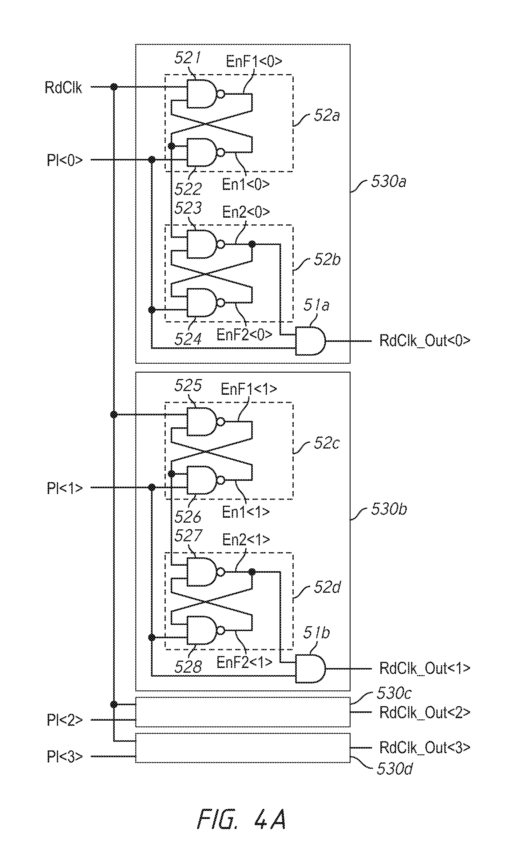
FIG. 4A is a diagram of cells of an input pointer register in a clock synchronizing circuit in accordance with an embodiment of the present disclosure. A cell [0] 530a, a cell 530b, a cell [2] 530c and a cell [3] 530d may be the cells [0]-[3] of the input pointer register 330 in the clock synchronizing circuit 30 of FIG. 3. The cells 530a, 530b, 530c and 530d may receive a command delay line input signal RdClk and may further provide pointer signals RdClk_Out<0>-<3> responsive to pointer input signals PI<0>-PI<3>, respectively. Each of the cells 530a, 530b, 530c and 530d includes two latches. For example, the cell [0] 530a includes an AND gate 51a and latches 52a and 52b. The latch 52a may include two NAND gates 521 and 522 and the latch 52b may include two NAND gates 523 and 524. Similarly, the cell [1] 530b includes an AND gate 51b and latches 52c and 52d. The latch 52c may include two NAND gates 525 and 526 and the latch 52d may include two NAND gates 527 and 528.
FIG. 4B is a timing diagram of signals in cells of the input pointer register of FIG. 4A, in accordance with an embodiment of the present disclosure. The pointer input signals PI<0>-PI<3> are a pulse signal having a pulse width 1T of command delay line input signal RdClk, where T is one clock cycle. The pointer input signals PI<0>-PI<3> are activated alternatively, in an order of PI<0>, PI<1>, PI<2>, PI<3>, and are provided by a decoder circuit, such as the decoder circuit 320 in FIG. 3.
For example, the cell [0] 530a receives the pointer input signal PI<0>. The NAND gate 522 in the latch 52a provides a signal En1<0> having a falling edge and a rising edge responsive to a rising edge and a falling edge of the pointer input signal PI<0> at time T1 and time 113, respectively, while a signal EnF1<0>, an output signal of the NAND gate 521, is inactive (e.g., at a logic low level). The NAND gate 521 provides a signal EnF1<0> having a falling edge responsive to the rising edge of the signal En1<0> at the time T3 and having a rising edge responsive to a falling edge of the command delay line input signal RdClk at time T4.
A signal En2<0> and the pointer input signal PI<0> are provided to the NAND gate 524 in the latch 52b. The NAND gate 524 in the latch 52b provides a signal EnF2<0> which is active (e.g., at a logic high level), responsive to the logic low level of the signal En2<0>, an output signal of the NAND gate 523, until the time 13 and further responsive to the logic low level of the pointer input signal PI<0> from the time T3. The NAND gate 523 in the latch 52b provides the signal En2<0> having a rising edge and a falling edge responsive to a falling edge and a rising edge of the signal EnF1<0> at the time T3 and the time T4 respectively, while the signal EnF2<0> is active (e.g., at the logic high level "High"). The AND gate 51a receives the pointer input signal PI<0> and the signal En2<0> and provides a pointer signal RdClk_Out<0> which is inactive (e.g., at the logic low level "Low").
At the same time, the cell [1]530b receives a pointer input signal PI<1>. The NAND gate 526 in the latch 52c provides a signal En1<1> having a falling edge responsive to the falling edge of the command delay line input signal RdClk at the time T4 and having a rising edge responsive to a falling edge of the pointer input signal PI<1> at time T5. The NAND gate 525 provides a signal EnF1<1> having a falling edge and a rising edge responsive to the rising edge and falling edge of the command delay line input signal RdClk at the time T2 and the time 14, respectively, while the signal En1<1> active (e.g., at the logic high level) until the time T4. A signal En2<1> and the pointer input signal PI<1> are provided to the NAND gate 528 in the latch 52d. The NAND gate 528 in the latch 52d provides a signal EnF2<1> having a falling edge and a rising edge responsive to the rising edge and the falling edge of the pointer input signal PI<1> at the time T3 and the time T5, respectively. The NAND gate 527 in the latch 52d provides the signal En2<1> having a rising edge responsive to the falling edge of the signal ErF1<1> and having a falling edge responsive to the rising edge of the signal EnF2<1>. The AND gate 51b receives the pointer input signal PI<1> and the signal En2<1> and provides a pointer signal RdClk_Out<1> that has a rising edge at the time T3 and a falling edge at the time T5.
Thus, the command delay line input signal RdClk may be captured by the pointer input signal PI<1> in the example of FIG. 4B. As described above, the latch 52a and the latch 52c capture the command delay line input signal RdClk by rising edges of the pointer input signals PI<0> and <1>, and the latch 52b and the latch 52d provide the pulse width 1T.
FIG. 5 is a circuit diagram of a command decoder circuit in an apparatus including a command delay adjustment circuit, in accordance with an embodiment of the present disclosure. The command decoder circuit 70 may latch commands on the command signals CMD with a clock signal GCLK based on the system clock signal SCLK_CMD before and after command decoding. In the command decoder circuit 70, the command signals CMD are provided to a buffer gate 73 that has a delay d1. The system clock signal SCLK_CMD is provided to a delay 71 to provide a delay d2, which is approximately equal to the delay d1 of the buffer gate 73, and the delay 71 provides the clock signal GCLK. A flip-flop 74 latches the delayed command signals from the buffer gate 73 with the clock signal GCLK. Output signals from the flip-flop 74 are provided to a decoder circuit 75. The decoder circuit 75 may decode the command based on the output signals from the flip-flop 74 and provides a signal, for example, a read signal, responsive to the output signals. A flip-flop 76 latches the signal from the decoder circuit 75 with the clock signal GCLK' and provides an internal read signal Rd. A delay 72 having a delay d3 receives the clock signal GCLK and provides a clock signal GCLK'. The delay d3 of the delay 72 may be equivalent to delays caused through the flip-flop 74, the decoder circuit 75 and the flip-flop 76. A flip-flop 77 latches the internal read signal Rd with the clock signal GCLK' and provides the enable signal Rdi to the clock input buffer 210. A buffer gate 78 having a delay d4 receives the internal read signal Rd and provides the command delay line input signal RdClk to the clock synchronizing circuit 231 of the command delay adjustment circuit 230 in FIG. 2. Thus, the time lag tDec, which is about a sum of the delays d1, d3 and d4, is provided to the command delay line input signal RdClk. The clock synchronizing circuit 231 is configured to absorb the time lag provided to the command delay line input signal RdClk.
FIG. 6 is a timing diagram of signals in an apparatus including a command delay adjustment circuit, in accordance with an embodiment of the present disclosure. After a DLL is reset or updated, the clock signal CK is provided to the clock input buffer 210 of the apparatus 200 in FIG. 2. The clock signal CK is clock pulse signal including rising edges at T0, T1, T2, T3, T4, T5, T6, T7, T8, T9, . . . , T16, T17 and so on. The clock input buffer 210 provides the system clock signal SCLK_CMD having a delay tIB at the clock input buffer 210 responsive to the clock signal CK. When a READ command is issued at T0, the command input buffer 211 receives the READ command on command signals MD and provides the command signals CMD to the command decoder circuit 220. The system clock signal SCLK_CMD has a rising edge with the delay tIB responsive to the rising edge of the clock signal CK at T0. A rising edge of the clock signal GCLK has the delay d2 from the rising edge of the system clock signal SCLK_CMD, due to the delay 71, equivalent to the delay d1 at the buffer gate 73, in FIG. 5. The enable signal Rdi has a rising edge with the delay d3 from the rising edge of clock signal GCLK. The command delay line input signal RdClk has a delay d4 from the enable signal Rdi caused by the buffer gate 78. Thus, the command delay line input signal RdClk has a delay of "tDec(=d2+d3+d4)." The enable signal Rdi may be reset by a burst end signal (not illustrated) after a read operation. In the clock synchronizing circuit 30, the delay circuit 340 provides a delay of "tDec+tSU" to the pointer input signals PI<3:0> from the system clock signal SCLK_CMD. In the timing diagram of FIG. 6, the pointer input signal PI<0> has the delay of "tDec+tSU" from the rising edge of the system clock signal SCLK_CMD at T0. Thus, the pointer input signal PI<0> has the delay tSU from the command delay line input signal RdClk that is a set up time of the command delay line input signal RdClk.
For example in the timing diagram of FIG. 6, a shift cycle parameter X in this example is three, which means that the RdClk_shift signal has a three-cycle delay from a corresponding pulse of the system clock signal SCLK_CMD. The pointer output signal PO<3> is activated just after the activation of the pointer input signal PI<0>. The pointer output signals PO<2>-PO<0> may maintain an inactive state (e.g., at the logic low level). Thus, the RdClk_shift signal is activated responsive to the pointer output signal PO<3>. The feedback clock signal SCLK_DLL_fb has a sum of a delay tIB at the clock input buffer 210, a delay tTREE at the TREE 290 and a delay tOB at the output buffer 295 from the DllClk. The N value in this example is five, which means that the feedback clock signal SCL_DLL_fb signal has a five-cycle delay from the corresponding pulse of the system clock signal SCLK_CMD. For example, the delayed read signal RdDll is latched with the falling edge of the DLL clock signal DllClk in the QED circuit 260 after the delay line 240 having a delay tDL. To ensure a latch margin "tlat" between the DLL clock signal DllClk and the delayed read signal RdDll in the QED circuit 260, the rising edges of the reference clock signal SCLK_DLL and rising edges of the clock-synchronized read signal RdClk_shift can be in synchronized by the clock synchronizing circuit 231 as described earlier. The QED circuit 260 synchronizes the delayed read signal RdDll with the DLL clock signal DllClk by shifting the delayed read signal RdDll by a total of (CL-N-X) cycles. Thus, output data on DQ signal has a delay that is a total of "tTree+tOB+(CL-N-X)*T" from the DLL clock signal DllClk.
Those of ordinary skill would further appreciate that the various illustrative logical blocks, configurations, modules, circuits, and algorithm steps described in connection with the embodiments disclosed herein may be implemented as electronic hardware, computer software executed by a processor, or combinations of both. Various illustrative components, blocks, configurations, modules, circuits, and steps have been described above generally in terms of their functionality. Skilled artisans may implement the described functionality in varying ways for each particular application, but such implementation decisions should not be interpreted as causing a departure from the scope of the present disclosure.
The previous description of the disclosed embodiments is provided to enable a person skilled in the art to make or use the disclosed embodiments. Various modifications to these embodiments will be readily apparent to those skilled in the art, and the principles defined herein may be applied to other embodiments without departing from the scope of the disclosure. Thus, the present disclosure is not intended to be limited to the embodiments shown herein but is to be accorded the widest scope possible consistent with the principles and novel features as defined by the following claims.
* * * * *
D00000
D00001
D00002
D00003
D00004
D00005
D00006
D00007
XML
uspto.report is an independent third-party trademark research tool that is not affiliated, endorsed, or sponsored by the United States Patent and Trademark Office (USPTO) or any other governmental organization. The information provided by uspto.report is based on publicly available data at the time of writing and is intended for informational purposes only.
While we strive to provide accurate and up-to-date information, we do not guarantee the accuracy, completeness, reliability, or suitability of the information displayed on this site. The use of this site is at your own risk. Any reliance you place on such information is therefore strictly at your own risk.
All official trademark data, including owner information, should be verified by visiting the official USPTO website at www.uspto.gov. This site is not intended to replace professional legal advice and should not be used as a substitute for consulting with a legal professional who is knowledgeable about trademark law.