Multi-path analog front end with adaptive path
Schneider , et al. April 16, 2
U.S. patent number 10,263,630 [Application Number 15/234,741] was granted by the patent office on 2019-04-16 for multi-path analog front end with adaptive path. This patent grant is currently assigned to Cirrus Logic, Inc.. The grantee listed for this patent is Cirrus Logic International Semiconductor Ltd.. Invention is credited to Daniel J. Allen, Aniruddha Satoskar, Edmund Mark Schneider, Saurabh Singh.


| United States Patent | 10,263,630 |
| Schneider , et al. | April 16, 2019 |
Multi-path analog front end with adaptive path
Abstract
In accordance with embodiments of the present disclosure, a processing system may include a plurality of processing paths and a controller. The plurality of processing paths may include a static processing path configured to generate a first digital signal based on an analog input signal and a dynamic processing path configured to generate a second digital signal based on the analog input signal, wherein a parameter of the dynamic processing path is determined based on a characteristic of the analog input signal. The controller may be configured to select the first digital signal as a digital output signal of the processing system when a change is occurring to the characteristic and select the second digital signal as the digital output signal in the absence of change occurring to the characteristic.
| Inventors: | Schneider; Edmund Mark (Austin, TX), Allen; Daniel J. (Austin, TX), Singh; Saurabh (Cedar Park, TX), Satoskar; Aniruddha (Austin, TX) | ||||||||||
|---|---|---|---|---|---|---|---|---|---|---|---|
| Applicant: |
|
||||||||||
| Assignee: | Cirrus Logic, Inc. (Austin,
TX) |
||||||||||
| Family ID: | 58486734 | ||||||||||
| Appl. No.: | 15/234,741 | ||||||||||
| Filed: | August 11, 2016 |
Prior Publication Data
| Document Identifier | Publication Date | |
|---|---|---|
| US 20180048325 A1 | Feb 15, 2018 | |
| Current U.S. Class: | 1/1 |
| Current CPC Class: | H03M 1/188 (20130101); H03M 1/0881 (20130101); G06F 13/4282 (20130101); H03M 1/0872 (20130101); G06F 13/4022 (20130101); H03M 1/12 (20130101) |
| Current International Class: | G06F 13/40 (20060101); G06F 13/42 (20060101); H03M 1/08 (20060101); H03M 1/18 (20060101); H03M 1/12 (20060101) |
| Field of Search: | ;710/316 |
References Cited [Referenced By]
U.S. Patent Documents
| 4346349 | August 1982 | Yokoyama |
| 4441081 | April 1984 | Jenkins |
| 4446440 | May 1984 | Bell |
| 4493091 | January 1985 | Gundry |
| 4890107 | December 1989 | Pearce |
| 4972436 | November 1990 | Halim et al. |
| 4999628 | March 1991 | Kakaubo et al. |
| 4999830 | March 1991 | Agazzi |
| 5077539 | December 1991 | Howatt |
| 5148167 | September 1992 | Ribner |
| 5198814 | March 1993 | Ogawara et al. |
| 5272449 | December 1993 | Izawa |
| 5321758 | June 1994 | Charpentier et al. |
| 5323159 | June 1994 | Imamura et al. |
| 5343161 | August 1994 | Tokumo et al. |
| 5550923 | July 1996 | Hotvet et al. |
| 5600317 | February 1997 | Knoth et al. |
| 5714956 | February 1998 | Jahne et al. |
| 5719641 | February 1998 | Mizoguchi |
| 5796303 | August 1998 | Vinn et al. |
| 5808575 | September 1998 | Himeno et al. |
| 5810477 | September 1998 | Abraham et al. |
| 6088461 | July 2000 | Lin |
| 6160455 | December 2000 | French et al. |
| 6201490 | March 2001 | Kawano et al. |
| 6271780 | August 2001 | Gong et al. |
| 6333707 | December 2001 | Oberhammer et al. |
| 6353404 | March 2002 | Kuroiwa |
| 6542612 | April 2003 | Needham |
| 6614297 | September 2003 | Score et al. |
| 6683494 | January 2004 | Stanley |
| 6745355 | June 2004 | Tamura |
| 6768443 | July 2004 | Willis |
| 6822595 | November 2004 | Robinson |
| 6853242 | February 2005 | Melanson et al. |
| 6888888 | May 2005 | Tu et al. |
| 6897794 | May 2005 | Kuyel et al. |
| 6989955 | January 2006 | Ziemer et al. |
| 7020892 | March 2006 | Levesque et al. |
| 7023268 | April 2006 | Taylor et al. |
| 7061312 | June 2006 | Andersen et al. |
| 7167112 | January 2007 | Andersen et al. |
| 7216249 | May 2007 | Fujiwara et al. |
| 7279964 | October 2007 | Bolz et al. |
| 7302354 | November 2007 | Zhuge |
| 7312734 | December 2007 | McNeill et al. |
| 7315204 | January 2008 | Seven |
| 7365664 | April 2008 | Caduff et al. |
| 7378902 | May 2008 | Sorrells et al. |
| 7385443 | June 2008 | Denison |
| 7403010 | July 2008 | Hertz |
| 7440891 | October 2008 | Shozakai et al. |
| 7522677 | April 2009 | Liang |
| 7583215 | September 2009 | Yamamoto et al. |
| 7671768 | March 2010 | De Ceuninck |
| 7679538 | March 2010 | Tsang |
| 7737776 | June 2010 | Cyrusian |
| 7893856 | February 2011 | Ek et al. |
| 7924189 | April 2011 | Sayers |
| 7937106 | May 2011 | Sorrells et al. |
| 7952502 | May 2011 | Kolze |
| 8060663 | November 2011 | Murray et al. |
| 8130126 | March 2012 | Breitschaedel et al. |
| 8194889 | June 2012 | Seefeldt |
| 8298425 | October 2012 | Kanbe |
| 8330631 | December 2012 | Kumar et al. |
| 8362936 | January 2013 | Ledzius et al. |
| 8462035 | June 2013 | Schimper et al. |
| 8483753 | July 2013 | Behzad et al. |
| 8508397 | August 2013 | Hisch |
| 8717211 | May 2014 | Miao et al. |
| 8786477 | July 2014 | Albinet |
| 8836551 | September 2014 | Nozaki |
| 8873182 | October 2014 | Liao |
| 8878708 | November 2014 | Sanders et al. |
| 8952837 | February 2015 | Kim et al. |
| 9071201 | June 2015 | Jones et al. |
| 9071267 | June 2015 | Schneider et al. |
| 9071268 | June 2015 | Schneider et al. |
| 9118401 | August 2015 | Nieto et al. |
| 9148164 | September 2015 | Schneider et al. |
| 9171552 | October 2015 | Yang |
| 9178462 | November 2015 | Kurosawa et al. |
| 9210506 | December 2015 | Nawfal et al. |
| 9337795 | May 2016 | Das et al. |
| 9391576 | July 2016 | Satoskar et al. |
| 9444504 | September 2016 | Robinson |
| 9503027 | November 2016 | Zanbaghi |
| 9525940 | December 2016 | Schneider et al. |
| 9543975 | January 2017 | Melanson et al. |
| 9584911 | February 2017 | Das et al. |
| 9596537 | March 2017 | He et al. |
| 9635310 | April 2017 | Chang et al. |
| 9680488 | June 2017 | Das et al. |
| 9762255 | September 2017 | Satoskar et al. |
| 9774342 | September 2017 | Schneider et al. |
| 9780800 | October 2017 | Satoskar et al. |
| 9807504 | October 2017 | Melanson et al. |
| 9813814 | November 2017 | Satoskar |
| 9831843 | November 2017 | Das et al. |
| 9917557 | March 2018 | Zhu et al. |
| 9929703 | March 2018 | Zhao |
| 2001/0001547 | May 2001 | Delano et al. |
| 2001/0009565 | July 2001 | Singvall |
| 2004/0078200 | April 2004 | Alves |
| 2004/0184621 | September 2004 | Andersen et al. |
| 2005/0068097 | March 2005 | Kim et al. |
| 2005/0084037 | April 2005 | Liang |
| 2005/0258989 | November 2005 | Li et al. |
| 2005/0276359 | December 2005 | Xiong |
| 2006/0056491 | March 2006 | Lim et al. |
| 2006/0064037 | March 2006 | Shalon et al. |
| 2006/0098827 | May 2006 | Paddock et al. |
| 2006/0261886 | November 2006 | Hansen et al. |
| 2006/0284675 | December 2006 | Krochmal et al. |
| 2007/0018719 | January 2007 | Seven |
| 2007/0026837 | February 2007 | Bagchi |
| 2007/0057720 | March 2007 | Hand et al. |
| 2007/0092089 | April 2007 | Seefeldt et al. |
| 2007/0103355 | May 2007 | Yamada |
| 2007/0120721 | May 2007 | Caduff |
| 2007/0123184 | May 2007 | Nesimoglu et al. |
| 2007/0146069 | June 2007 | Wu et al. |
| 2008/0012639 | January 2008 | Mels |
| 2008/0030577 | February 2008 | Cleary et al. |
| 2008/0114239 | May 2008 | Randall et al. |
| 2008/0143436 | June 2008 | Xu |
| 2008/0159444 | July 2008 | Terada |
| 2008/0198048 | August 2008 | Klein et al. |
| 2008/0292107 | November 2008 | Bizjak |
| 2009/0015327 | January 2009 | Wu et al. |
| 2009/0021643 | January 2009 | Hsueh et al. |
| 2009/0051423 | February 2009 | Miaille et al. |
| 2009/0058531 | March 2009 | Hwang et al. |
| 2009/0084586 | April 2009 | Nielsen |
| 2009/0220110 | September 2009 | Bazarjani et al. |
| 2010/0168882 | July 2010 | Zhang et al. |
| 2010/0176980 | July 2010 | Breitschadel et al. |
| 2010/0183163 | July 2010 | Matsui et al. |
| 2011/0013733 | January 2011 | Martens et al. |
| 2011/0025540 | February 2011 | Katsis |
| 2011/0029109 | February 2011 | Thomsen et al. |
| 2011/0063148 | March 2011 | Kolze et al. |
| 2011/0096370 | April 2011 | Okamoto |
| 2011/0134980 | June 2011 | Lipka |
| 2011/0136455 | June 2011 | Sundstrom et al. |
| 2011/0150240 | June 2011 | Akiyama et al. |
| 2011/0170709 | July 2011 | Guthrie et al. |
| 2011/0188671 | August 2011 | Anderson et al. |
| 2011/0228952 | September 2011 | Lin |
| 2011/0242614 | October 2011 | Okada |
| 2011/0268301 | November 2011 | Nielsen et al. |
| 2011/0285463 | November 2011 | Walker et al. |
| 2012/0001786 | January 2012 | Hisch |
| 2012/0047535 | February 2012 | Bennett et al. |
| 2012/0133411 | May 2012 | Miao et al. |
| 2012/0177201 | July 2012 | Ayling et al. |
| 2012/0177226 | July 2012 | Silverstein et al. |
| 2012/0188111 | July 2012 | Ledzius et al. |
| 2012/0207315 | August 2012 | Kimura et al. |
| 2012/0242521 | September 2012 | Kinyua |
| 2012/0250893 | October 2012 | Carroll et al. |
| 2012/0263090 | October 2012 | Porat et al. |
| 2012/0274490 | November 2012 | Kidambi et al. |
| 2012/0280726 | November 2012 | Colombo et al. |
| 2012/0293348 | November 2012 | Snelgrove |
| 2013/0095870 | April 2013 | Phillips et al. |
| 2013/0106635 | May 2013 | Doi |
| 2013/0129117 | May 2013 | Thomsen et al. |
| 2013/0188808 | July 2013 | Pereira et al. |
| 2013/0241753 | September 2013 | Nozaki |
| 2013/0241755 | September 2013 | Chen et al. |
| 2014/0044280 | February 2014 | Jiang |
| 2014/0105256 | April 2014 | Hanevich et al. |
| 2014/0105273 | April 2014 | Chen et al. |
| 2014/0126747 | May 2014 | Huang |
| 2014/0135077 | May 2014 | Leviant et al. |
| 2014/0184332 | July 2014 | Shi et al. |
| 2014/0269118 | September 2014 | Taylor et al. |
| 2014/0368364 | December 2014 | Hsu |
| 2015/0009079 | January 2015 | Bojer |
| 2015/0170663 | June 2015 | Disch et al. |
| 2015/0214974 | July 2015 | Currivan |
| 2015/0214975 | July 2015 | Gomez et al. |
| 2015/0249466 | September 2015 | Elyada |
| 2015/0295584 | October 2015 | Das et al. |
| 2015/0327174 | November 2015 | Rajagopal et al. |
| 2015/0381130 | December 2015 | Das et al. |
| 2016/0072465 | March 2016 | Das et al. |
| 2016/0080862 | March 2016 | He et al. |
| 2016/0080865 | March 2016 | He et al. |
| 2016/0139230 | May 2016 | Petrie et al. |
| 2016/0173112 | June 2016 | Das et al. |
| 2016/0181988 | June 2016 | Du et al. |
| 2016/0286310 | September 2016 | Das et al. |
| 2016/0365081 | December 2016 | Satoskar et al. |
| 2017/0047895 | February 2017 | Zanbaghi |
| 2017/0150257 | May 2017 | Das et al. |
| 2017/0212721 | July 2017 | Satoskar et al. |
| 2018/0046239 | February 2018 | Schneider |
| 2018/0048325 | February 2018 | Schneider |
| 2018/0098149 | April 2018 | Das |
| 0351788 | Jul 1989 | EP | |||
| 0966105 | Dec 1999 | EP | |||
| 1244218 | Sep 2002 | EP | |||
| 1575164 | Sep 2005 | EP | |||
| 1689075 | Aug 2006 | EP | |||
| 1753130 | Feb 2007 | EP | |||
| 1798852 | Jun 2009 | EP | |||
| 2207264 | Jul 2010 | EP | |||
| 1599401 | Sep 1981 | GB | |||
| 2307121 | Jun 1997 | GB | |||
| 2507096 | Apr 2014 | GB | |||
| 2527637 | Dec 2015 | GB | |||
| 2527677 | Oct 2016 | GB | |||
| 2537694 | Oct 2016 | GB | |||
| 2537697 | Oct 2016 | GB | |||
| 2539517 | Dec 2016 | GB | |||
| 2552860 | Feb 2018 | GB | |||
| 2552867 | Feb 2018 | GB | |||
| 2008294803 | Dec 2008 | JP | |||
| WO0054403 | Sep 2000 | WO | |||
| 02/37686 | May 2002 | WO | |||
| 2006018750 | Feb 2006 | WO | |||
| 2007005380 | Jan 2007 | WO | |||
| 2007136800 | Nov 2007 | WO | |||
| 2008067260 | Jun 2008 | WO | |||
| 2014113471 | Jul 2014 | WO | |||
| 2015160655 | Oct 2015 | WO | |||
| 2016040165 | Mar 2016 | WO | |||
| 2016040171 | Mar 2016 | WO | |||
| 2016040177 | Mar 2016 | WO | |||
| 2016160336 | Oct 2016 | WO | |||
| 2016202636 | Dec 2016 | WO | |||
| 2017116629 | Jul 2017 | WO | |||
| 2018031525 | Feb 2018 | WO | |||
| 2018031646 | Feb 2018 | WO | |||
Other References
|
International Search Report and Written Opinion of the International Searching Authority, International Application No. PCT/US2016/040096, dated Mar. 24, 2017. cited by applicant . International Search Report and Written Opinion of the International Searching Authority, International Application No. PCT/US2017/014240, dated Apr. 24, 2017. cited by applicant . Groeneweg, B.P., et al., A Class-AB/D Audio Power Amplifier for Mobile Applications Integrated Into a 2.5G/3G Baseband Processo1016r, IEEE Transactions on Circuits and Systems--I: Regular Papers, vol. 57, No. 5, May 2010, pp. 1003-1016. cited by applicant . Chen, K., et al., A High-PSRR Reconfigurable Class-AB/D Audio. Amplifier Driving a Hands-Free/Receiver. 2-in-1 Loudspeaker, IEEE Journal of Solid-State Circuits, vol. 47, No. 11, Nov. 2012, pp. 2586-2603. cited by applicant . Thaden, Rainer et al., A Loudspeaker Management System with FIR/IRR Filtering; AES 32nd International Conference, Hillerod, Denmark, Sep. 21-23, 2007; pp. 1-12. cited by applicant . Thaden, Rainer et al., A Loudspeaker Management System with FIR/IRR Filtering; Slides from a presentation given at the 32nd AES conference "DSP for Loudspeakers" in Hillerod, Denmark in Sep. 2007; http://www.four-audio.com/data/AES32/AES32FourAudio.pdf; 23 pages. cited by applicant . GB Patent Application No. 1419651.3, Improved Analogue-to-Digital Convertor, filed Nov. 4, 2014, 65 pages. cited by applicant . Combined Search and Examination Report, GB Application No. GB1506258.1, dated Oct. 21, 2015, 6 pages. cited by applicant . International Search Report and Written Opinion, International Patent Application No. PCT/US2015/025329, dated Aug. 11, 2015, 9 pages. cited by applicant . International Search Report and Written Opinion, International Patent Application No. PCT/US2015/048633, dated Dec. 10, 2015, 11 pages. cited by applicant . International Search Report and Written Opinion, International Patent Application No. PCT/US2015/048591, dated Dec. 10, 2015, 11 pages. cited by applicant . Combined Search and Examination Report, GB Application No. GB1510578.6, dated Aug. 3, 2015, 3 pages. cited by applicant . International Search Report and Written Opinion, International Application No. PCT/US2015/056357, dated Jan. 29, 2015, 13 pages. cited by applicant . Combined Search and Examination Report, GB Application No. GB1514512.1, dated Feb. 11, 2016, 7 pages. cited by applicant . International Search Report and Written Opinion, International Application No. PCT/US2015/048609, dated Mar. 23, 2016, 23 pages. cited by applicant . International Search Report and Written Opinion, International Application No. PCT/US2016/022578, dated Jun. 22, 2016, 12 pages. cited by applicant . Combined Search and Examination Report, GB Application No. GB1600528.2, dated Jul. 7, 2016, 8 pages. cited by applicant . Combined Search and Examination Report, GB Application No. GB1603628.7, dated Aug. 24, 2016, 6 pages. cited by applicant . International Search Report and Written Opinion, International Application No. PCT/EP2016/062862, dated Aug. 26, 2016, 14 pages. cited by applicant . Combined Search and Examination Report under Sections 17 and 18(3) of the UKIPO, Application No. GB1620427.3, dated Jun. 1, 2017. cited by applicant . Combined Search and Examination Report under Sections 17 and 18(3) of the UKIPO, Application No. GB1620428.1, dated Jul. 21, 2017. cited by applicant . Combined Search and Examination Report under Sections 17 and 18(3), United Kingdom Intellectual Property Office, Application No. GB1700371.6, dated Aug. 1, 2017. cited by applicant . Combined Search and Examination Report under Sections 17 and 18(3), United Kingdom Intellectual Property Office, Application No. GB1702540.4, dated Oct. 2, 2017. cited by applicant . Combined Search and Examination Report under Sections 17 and 18(3), United Kingdom Intellectual Property Office, Application No. GB1702655.0, dated Oct. 24, 2017. cited by applicant . Combined Search and Examination Report under Sections 17 and 18(3), United Kingdom Intellectual Property Office, Application No. GB1706693.7, dated Oct. 26, 2017. cited by applicant . Combined Search and Examination Report under Sections 17 and 18(3), United Kingdom Intellectual Property Office, Application No. GB1706690.3, dated Oct. 30, 2017. cited by applicant . Search Report under Section 17, United Kingdom Intellectual Property Office, Application No. GB1702656.8, dated Oct. 31, 2017. cited by applicant . International Search Report and Written Opinion of the International Searching Authority, International Patent Application No. PCT/US2017/045861, dated Nov. 14, 2017. cited by applicant . International Search Report and Written Opinion of the International Searching Authority, International Patent Application No. PCT/US2017/046083, dated Nov. 14, 2017. cited by applicant . Combined Search and Examination Report under Sections 17 and 18(3), United Kingdom Intellectual Property Office, Application No. GB1708546.5, dated Nov. 22, 2017. cited by applicant . Combined Search and Examination Report under Sections 17 and 18(3), United Kingdom Intellectual Property Office, Application No. GB1708544.0, dated Nov. 28, 2017. cited by applicant . International Search Report and Written Opinion of the International Searching Authority, International Patent Application No. PCT/US2017/052439, dated Dec. 14, 2017. cited by applicant . Chen, Kuo-Hsin, et al., A 106dB PSRR Direct Battery Connected Reconfigurable Class-AB/D Speaker Amplifier for Hands-Free/Receiver 2-in-1 Loudspeaker, Solid State Circuits Conference (A-SSCC), 2011 IEEE Asian, Nov. 14, 2011, pp. 221-224. cited by applicant . Combined Search and Examination Report, GB Application No. GB1602288.1, dated Aug. 9, 2016, 6 pages. cited by applicant . International Search Report and Written Opinion of the International Searching Authority, International Application No. PCT/US2016/065134, dated Mar. 15, 2017. cited by applicant . Examination Report under Section 18(3), UKIPO, Application No. GB1702656.8, dated Jan. 17, 2019. cited by applicant. |
Primary Examiner: Mamo; Elias
Attorney, Agent or Firm: Jackson Walker L.L.P.
Claims
What is claimed is:
1. A processing system comprising: a plurality of processing paths comprising: a static processing path configured to generate a first digital signal based on an analog input signal, wherein a gain parameter of the static processing path does not vary based on the analog input signal; and a dynamic processing path configured to generate a second digital signal based on the analog input signal, wherein a parameter of the dynamic processing path is dynamically determined based on a characteristic of the analog input signal such that different values of the characteristic of the analog input signal correspond to different values of the parameter of the dynamic processing path; and a controller configured to select the first digital signal as a digital output signal of the processing system when a change is occurring to the characteristic and select the second digital signal as the digital output signal in an absence of change occurring to the characteristic; wherein the parameter of the dynamic processing path comprises one of a gain of the dynamic processing path, a bandwidth of the dynamic processing path, a filter configuration gain of the dynamic processing path, a noise floor of the dynamic processing path, a distortion of the dynamic processing path, and a power consumed by the dynamic processing path.
2. The processing system of claim 1, wherein the characteristic comprises one of a magnitude of the analog input signal, a spectral content of the analog input signal, a noise floor of the analog input signal, a distortion of the analog input signal, a signal-to-noise ratio of the analog input signal, and a required resolution of the analog input signal.
3. The processing system of claim 1, wherein the controller is further configured to change selection from the first digital signal as the digital output signal to the second digital signal as the digital output signal in response to passage of a duration of time after the parameter of the dynamic processing path changed in response to the change to the characteristic.
4. The processing system of claim 1, wherein the controller is further configured to, when selecting the first digital signal as the digital output signal, transition continuously or in steps the digital output signal between the second digital signal and the first digital signal during a duration of time, and such that during such transition, the digital output signal is a weighted average of the first digital signal and the second digital signal wherein a weight of the first digital signal relative to a weight of the second digital signal is configured to increase during the transition.
5. The processing system of claim 1, wherein the controller is further configured to, when selecting the second digital signal as the digital output signal, transition continuously or in steps the digital output signal between the first digital signal and the second digital signal, wherein a rate of the transition is based on a magnitude of the analog input signal, and such that during such transition, the digital output signal is a weighted average of the first digital signal and the second digital signal, wherein a weight of the second digital signal relative to a weight of the first digital signal is configured to increase during the transition.
6. The processing system of claim 5, wherein the controller is further configured to transition the digital output signal between the first digital signal and the second digital signal over a maximum duration of time, wherein the maximum duration of time is independent of the magnitude of the analog input signal.
7. A method comprising: generating a first digital signal based on an analog input signal with a static processing path, wherein a gain parameter of the static processing path does not vary based on the analog input signal; generating a second digital signal based on an analog input signal with a dynamic processing path, wherein a parameter of the dynamic processing path is dynamically determined based on a characteristic of the analog input signal such that different values of the characteristic of the analog input signal correspond to different values of the parameter of the dynamic processing path; and selecting the first digital signal as a digital output signal of a processing system when a change is occurring to the characteristic and selecting the second digital signal as the digital output signal in an absence of change occurring to the characteristic; wherein the parameter of the dynamic processing path comprises one of a gain of the dynamic processing path, a bandwidth of the dynamic processing path, a filter configuration gain of the dynamic processing path, a noise floor of the dynamic processing path, a distortion of the dynamic processing path, and a power consumed by the dynamic processing path.
8. The method of claim 7, wherein the characteristic comprises one of a magnitude of the analog input signal, a spectral content of the analog input signal, a noise floor of the analog input signal, a distortion of the analog input signal, a signal-to-noise ratio of the analog input signal, and a required resolution of the analog input signal.
9. The method of claim 7, further comprising changing selection from the first digital signal as the digital output signal to the second digital signal as the digital output signal in response to passage of a duration of time after the parameter of the dynamic processing path changed in response to the change to the characteristic.
10. The method of claim 7, further comprising, when selecting the first digital signal as the digital output signal, transitioning continuously or in steps the digital output signal between the second digital signal and the first digital signal during a duration of time, and such that during such transition, the digital output signal is a weighted average of the first digital signal and the second digital signal wherein a weight of the first digital signal relative to a weight of the second digital signal increases during the transition.
11. The method of claim 7, further comprising, when selecting the second digital signal as the digital output signal, transitioning continuously or in steps the digital output signal between the first digital signal and the second digital signal, wherein a rate of the transition is based on a magnitude of the analog input signal, and such that during such transition, the digital output signal is a weighted average of the first digital signal and the second digital signal, wherein a weight of the second digital signal relative to a weight of the first digital signal increases during the transition.
12. The method of claim 11, further comprising transitioning the digital output signal between the first digital signal and the second digital signal over a maximum duration of time, wherein the maximum duration of time is independent of the magnitude of the analog input signal.
Description
FIELD OF DISCLOSURE
The present disclosure relates in general to signal processing systems, and more particularly, to multiple path signal processing systems.
BACKGROUND
The use of multipath analog-to-digital converters (ADCs) and analog front ends (AFEs) (e.g., two or more path ADCs/AFEs) in electrical circuits is known. Example multipath ADCs and AFEs and use of them in multiple electrical circuit paths are disclosed in U.S. Pat. No. 5,714,956 entitled "Process and System for the Analog-to-Digital Conversion of Signals" to Jahne et al. ("Jahne patent"), U.S. Pat. No. 5,600,317 entitled "Apparatus for the Conversion of Analog Audio Signals to a Digital Data Stream" to Knoth et al. ("Knoth patent") and U.S. Pat. No. 6,271,780 entitled "Gain Ranging Analog-to-Digital Converter with Error Correction" to Gong et al. ("Gong patent"). The use of multipath circuits may reduce noise as one path may be optimized for processing small amplitude signals (e.g., for processing low noise signals) while another circuit path with another set of ADC and AFE is optimized for large amplitude signals (e.g., allowing for higher dynamic range).
An example application for multipath ADCs/AFEs is use of them in a circuit for an audio system application, such as an audio mixing board or in a digital microphone system. Such an example application is disclosed in the Jahne patent. In designing a circuit with multipath ADCs/AFEs that are used in respective multiple circuit paths, a tradeoff may exist between allowing larger signal swing (e.g., to allow swing of a signal between larger scale amplitudes) and low noise. Furthermore, the multipath ADCs/AFEs may provide high dynamic range signal digitization, with higher dynamic range for a given input power, and lower overall area than would be possible with conventional means. In other words, by allowing a separate optimization for each type of signal (e.g., large and small signals) that is provided each respective path, multipath ADCs/AFEs allow the overall circuit to burn less power, consume less area, and save on other such design costs.
SUMMARY
In accordance with the teachings of the present disclosure, certain disadvantages and problems associated with implementation of a multiple AFE/ADC path may be reduced or eliminated.
In accordance with embodiments of the present disclosure, a processing system may include a plurality of processing paths and a controller. The plurality of processing paths may include a static processing path configured to generate a first digital signal based on an analog input signal and a dynamic processing path configured to generate a second digital signal based on the analog input signal, wherein a parameter of the dynamic processing path is determined based on a characteristic of the analog input signal. The controller may be configured to select the first digital signal as a digital output signal of the processing system when a change is occurring to the characteristic and select the second digital signal as the digital output signal in the absence of change occurring to the characteristic.
In accordance with these and other embodiments of the present disclosure, a method may include generating a first digital signal based on an analog input signal with a static processing path, generating a second digital signal based on an analog input signal with a dynamic processing path, wherein a parameter of the dynamic processing path is determined based on a characteristic of the analog input signal, and selecting the first digital signal as a digital output signal of the processing system when a change is occurring to the characteristic and selecting the second digital signal as the digital output signal in the absence of change occurring to the characteristic.
Technical advantages of the present disclosure may be readily apparent to one having ordinary skill in the art from the figures, description and claims included herein. The objects and advantages of the embodiments will be realized and achieved at least by the elements, features, and combinations particularly pointed out in the claims.
It is to be understood that both the foregoing general description and the following detailed description are explanatory examples and are not restrictive of the claims set forth in this disclosure.
BRIEF DESCRIPTION OF THE DRAWINGS
A more complete understanding of the present embodiments and advantages thereof may be acquired by referring to the following description taken in conjunction with the accompanying drawings, in which like reference numbers indicate like features, and wherein:
FIG. 1 illustrates a block diagram of selected components of an example signal processing system, in accordance with embodiments of the present disclosure;
FIG. 2 illustrates a block diagram of selected components of an integrated circuit for processing an analog signal to generate a digital signal, in accordance with embodiments of the present disclosure; and
FIG. 3 illustrates a block diagram of selected components of the integrated circuit of FIG. 2 depicting selected components of example embodiments of analog front ends and analog-to-digital converters, in accordance with embodiments of the present disclosure.
DETAILED DESCRIPTION
FIG. 1 illustrates a block diagram of selected components of an example signal processing system 100, in accordance with embodiments of the present disclosure. As shown in FIG. 1, signal processing system 100 may include an analog signal source 101, an integrated circuit (IC) 105, and a digital audio processor 109. Analog signal source 101 may comprise any system, device, or apparatus configured to generate an analog electrical signal, for example an analog input signal ANALOG_IN. For example, in embodiments in which signal processing system 100 is a processing system, analog signal source 101 may comprise a microphone transducer.
Integrated circuit 105 may comprise any suitable system, device, or apparatus configured to process analog input signal ANALOG_IN to generate a digital output signal DIGITAL_OUT and condition digital output signal DIGITAL_OUT for transmission over a bus to digital processor 109. Once converted to digital output signal DIGITAL_OUT, the signal may be transmitted over significantly longer distances without being susceptible to noise as compared to an analog transmission over the same distance. In some embodiments, integrated circuit 105 may be disposed in close proximity with analog signal source 101 to ensure that the length of the analog line between analog signal source 101 and integrated circuit 105 is relatively short to minimize the amount of noise that can be picked up on an analog output line carrying analog input signal ANALOG_IN. For example, in some embodiments, analog signal source 101 and integrated circuit 105 may be formed on the same substrate. In other embodiments, analog signal source 101 and integrated circuit 105 may be formed on different substrates packaged within the same integrated circuit package.
Digital processor 109 may comprise any suitable system, device, or apparatus configured to process a digital output signal for use in a digital system. For example, digital processor 109 may comprise a microprocessor, microcontroller, digital signal processor (DSP), application specific integrated circuit (ASIC), or any other device configured to interpret and/or execute program instructions and/or process data, such as digital output signal DIGITAL_OUT.
Signal processing system 100 may be used in any application in which it is desired to process an analog signal to generate a digital signal. Thus, in some embodiments, signal processing system 100 may be integral to an audio device that converts analog signals (e.g., from a microphone) to digital signals representing the sound incident on a microphone. As another example, signal processing system 100 may be integral to a radio-frequency device (e.g., a mobile telephone) to convert radio-frequency analog signals into digital signals.
FIG. 2 illustrates a block diagram of selected components of integrated circuit 105, in accordance with embodiments of the present disclosure. As shown in FIG. 2, integrated circuit 105 may include two or more processing paths 201a and 201b (which may be referred to herein individually as a processing path 201 and collectively as processing paths 201), each processing path 201 including a respective AFE 203 (e.g., AFE 203a, AFE 203b) and a respective ADC (e.g., ADC 215a, ADC 215b). An AFE 203 may receive analog input signal ANALOG_IN via one or more input lines which may allow for receipt of a single-ended signal, differential signal, or any other suitable analog signal format and may comprise any suitable system, device, or apparatus configured to condition analog input signal ANALOG_IN for processing by ADC 215. Selected components for example embodiments of AFEs 203a and 203b are discussed in greater detail below with respect to FIG. 3. The output of each AFE 203 may be communicated to a respective ADC 215 on one or more output lines.
An ADC 215 may comprise any suitable system, device, or apparatus configured to convert an analog signal received at its input, to a digital signal representative of analog input signal ANALOG_IN. ADC 215 may itself include one or more components (e.g., delta-sigma modulator, decimator, etc.) for carrying out the functionality of ADC 215. Selected components for the example embodiments of ADCs 215a and 215b are discussed in greater detail below with respect to FIG. 3.
A multiplexer 227 may receive a respective digital signal from each of processing paths 201 and may select one of the digital signals as digital output signal DIGITAL_OUT based on a control signal generated by and communicated from a controller 220.
Driver 219 may receive the digital signal DIGITAL_OUT output by ADC 215 and may comprise any suitable system, device, or apparatus configured to condition such digital signal (e.g., encoding into Audio Engineering Society/European Broadcasting Union (AES/EBU), Sony/Philips Digital Interface Format (S/PDIF)), in the process generating digital output signal DIGITAL_OUT for transmission over a bus to digital processor 109. In FIG. 2, the bus receiving digital output signal DIGITAL_OUT is shown as single-ended. In some embodiments, driver 219 may generate a differential digital output signal 107.
Controller 220 may comprise any suitable system, device, or apparatus for selecting one of the digital signals output by the various processing paths 201 as digital output signal DIGITAL_OUT. In some embodiments, controller 220 may make such selection based on a magnitude of analog input signal ANALOG_IN or a signal derivative thereof. For example, controller 220 may include an overload detector 221 that may determine whether or not a signal derivative of analog input signal ANALOG_IN (e.g., an output of a modulator 316a of delta-sigma modulator 308a, as shown in greater detail in FIG. 3) is likely to cause clipping or other distortion of digital output signal DIGITAL_OUT if a particular processing path (e.g., processing path 201a) is selected. If clipping or other distortion of digital output signal DIGITAL_OUT is likely if the particular processing path (e.g., processing path 201a) is selected, state machine 225 of controller 220 may generate a control signal so that another processing path (e.g., processing path 201b) is selected. To further illustrate, in some embodiments, processing path 201a may be a path adapted for low amplitudes of analog input signal ANALOG_IN and may thus have a high signal gain, while processing path 201b may be a path adapted for higher amplitudes of analog input signal ANALOG_IN and may thus have a lower signal gain. Thus, if analog input signal ANALOG_IN or a derivative thereof is greater than a threshold value indicative of a condition whereby digital output signal DIGITAL_OUT may experience clipping or other distortion if processing path 201a is selected, overload detector 221 may detect such condition, and cause state machine 225 to generate a control signal to select the digital signal generated by processing path 201b as digital output signal DIGITAL_OUT.
In operation, processing path 201a may be a dynamic processing path, in that one or more parameters of processing path 201a may be variable based on one or more characteristics of analog input signal ANALOG_IN, as described in greater detail elsewhere in this disclosure. Furthermore, processing path 201b may be a static processing path, in that similar parameters of processing path 201b may remain substantially fixed regardless of the one or more characteristics of analog input signal ANALOG_IN. Such one or more parameters may include a gain of processing path 201a, a bandwidth of processing path 201a, a filter configuration gain of processing path 201a, a noise floor of processing path 201a, a distortion of processing path 201a, and a power consumed by processing path 201a. Such one or more characteristics of analog input signal ANALOG_IN may include a magnitude of analog input signal ANALOG_IN, a spectral content of analog input signal ANALOG_IN, a noise floor of analog input signal ANALOG_IN, a distortion of analog input signal ANALOG_IN, a signal-to-noise ratio of analog input signal ANALOG_IN, and a required resolution of analog input signal ANALOG_IN.
To that end, controller 220 may include a level detector 223 that may detect an amplitude of analog input signal ANALOG_IN or a signal derivative thereof (e.g., a signal generated within ADC 215b) and communicate a signal indicative of such amplitude to state machine 225 and may also include an input signal analysis block 228 which may analyze or otherwise process a digital signal derived from analog input signal ANALOG_IN to determine one or more characteristics of analog input signal ANALOG_IN other than its magnitude and communicate a signal indicative of such amplitude to state machine 225. Based on such characteristics, state machine 225 of controller 220 may issue parameter control signals to one or more components of processing path 201a in order to set one or more parameters of processing path 201a based on the one or more characteristics of analog input signal ANALOG_IN.
In addition, state machine 225 of controller 220 may be configured to select the digital signal generated by processing path 201b as digital output signal DIGITAL_OUT when a change is occurring to a characteristic of analog input signal ANALOG_IN (such that a corresponding change is made to one or more parameters of processing path 201a in response to the change in the characteristic) and select the digital signal generated by processing path 201a as digital output signal DIGITAL_OUT in the absence of change occurring to characteristics of analog input signal ANALOG_IN. Thus, when a change is occurring to a characteristic of analog input signal ANALOG_IN such that a corresponding change is made to one or more parameters of processing path 201a in response to the change in the characteristic, controller 220 may select static processing path 201b to generate digital output signal DIGITAL_OUT so that a listener would not be subject to audio artifacts that may occur if a processing path with varying parameters was used to generate digital output signal DIGITAL_OUT. Accordingly, as one or more characteristics of analog input signal ANALOG_IN change, one or more parameters of dynamic processing path 201a may be optimized for performance, power, and/or other attribute (e.g., in order to maximize signal quality while minimizing power consumption).
To minimize the occurrence of audio artifacts occurring due to a change in a parameter of dynamic processing path 201a, controller 220 may be configured such that it changes selection from the digital signal generated by static processing path 201b as digital output signal DIGITAL_OUT to the digital signal generated by dynamic processing path 201a as digital output signal DIGITAL_OUT only after any transient effects of the change in a parameter of dynamic processing path 201a have settled. For example, in some embodiments, to ensure any such transient effects have settled, controller 220 may switch from static processing path 201b to dynamic processing path 201a in response to passage of a duration of time after the parameter of dynamic processing path 201a is changed.
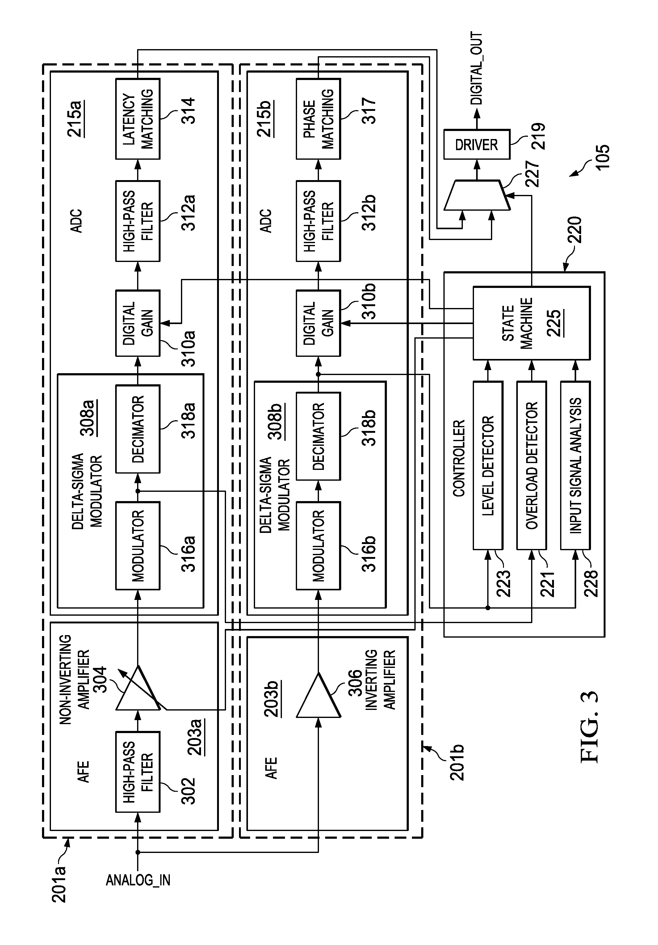
FIG. 3 illustrates a block diagram of selected components of integrated circuit 105 depicting selected components of example embodiments of AFEs 203 and ADCs 215, in accordance with embodiments of the present disclosure. As shown in FIG. 3, analog front end 203a of processing path 201a may include a high-pass filter 302 configured to high-pass filter analog input signal ANALOG_IN to remove direct current offsets or biases, which are often particularly troublesome for high-gain amplifiers, and output such filtered signal to a non-inverting amplifier 304. Non-inverting amplifier 304 may amplify analog input signal ANALOG_IN by a non-inverting gain and communicate such amplified analog signal to ADC 215a. In some embodiments, high-pass filter 302 may be formed on the same integrated circuit as one or more of AFE 203a, AFE 203b, ADC 215a, and ADC 215b. Because of the presence of high-pass filter 302 in processing path 201a, but not processing path 201b, processing paths 201 may each have a different frequency response to analog input signal ANALOG_IN.
Also as shown in FIG. 3, analog front end 203b of processing path 201b may include an inverting amplifier 306 which may amplify analog input signal ANALOG_IN by an inverting gain and communicate such amplified analog signal to ADC 215b. In some embodiments, inverting amplifier 306 may be configured to apply a multiplicative gain of less than unity to analog input signal ANALOG_IN. By attenuating higher-amplitude signals, a greater dynamic range for analog input signal ANALOG_IN may be achieved, in spite of conventional wisdom that would generally dictate that signal loss should be avoided in a low-noise system. In these and other embodiments, although not depicted in FIG. 3, inverting amplifier 306 may receive the output of high-pass filter 302 instead of the unfiltered analog input signal ANALOG_IN.
Although AFEs 203a and 203b are described above having a non-inverting gain and an inverting gain, respectively, each of processing paths 201 may have approximately the same cumulative gain. Those of skill in the art may appreciate that simply applying a digital gain with a negative sign in either of ADC 215a or ADC 215b will negate the opposite polarities of the gains of AFEs 203.
As depicted in FIG. 3, each ADC 215 may include a respective delta-sigma modulator 308 (e.g., delta-sigma modulators 308a and 308b), a respective digital gain element 310 (e.g., digital gain elements 310a and 310b), and respective high-pass filters 312 (e.g., high-pass filters 312a and 312b). Each delta-sigma modulator 308 may be configured to modulate an analog signal into a corresponding digital signal. As known in the art, each delta-sigma modulator 308 may include a respective modulator 316 (e.g., modulators 316a, 316b) and a decimator 318 (e.g., decimators 318a, 318b). Each digital gain element 310 may apply a gain to a digital signal generated by its associated delta-sigma modulator 308. Each high-pass filter 312 may high-pass filter a digital signal generated by its associated digital gain element, to filter out any direct-current offsets present in the digital signal. High-pass filter 312b may also compensate for high-pass filter 302 present in AFE 203a.
In addition, ADC 215a may comprise a latency matching element 314 to match any signal latencies between processing path 201a and processing path 201b, while ADC 215b may comprise a phase matching element 317 to account for any phase offset between processing path 201a and processing path 201b. For example, phase matching element 317 may dynamically compensate for any phase mismatch between processing paths 201a and 201b by varying a delay of at least one of processing path 201a and processing path 201b. In some embodiments, phase matching element 317 may comprise a high-pass filter.
In some embodiments, a magnitude of a gain of non-inverting amplifier 304 may be substantially larger than (e.g., significantly more than manufacturing tolerances, one or more orders of magnitude) a magnitude of a gain of inverting amplifier 306. In addition, in these and other embodiments, a magnitude of digital gain element 310b may be substantially larger than (e.g., significantly more than manufacturing tolerances, one or more orders of magnitude) a magnitude of a gain of digital gain element 310a. Consequently, in such embodiments, a first path gain equal to the product of the magnitude of the gain of inverting amplifier 306 and the magnitude of a gain of digital gain element 310b may be substantially equal (e.g., within manufacturing tolerances) to a second path gain equal to the product of the magnitude of gain of non-inverting amplifier 304 and the gain of digital gain element 310a. As a specific example, in some embodiments, the inverting gain of inverting amplifier 306 may be approximately -6 decibels, the non-inverting gain of non-inverting amplifier 304 may be approximately 20 decibels, the gain of digital gain element 310a may be approximately -26 decibels, and the gain of digital gain element 310b may be approximately 0 decibels.
Accordingly, each processing path 201 may be adapted to process a particular amplitude of analog input signal ANALOG_IN. For example, AFE 203a may be suited to process lower signal amplitudes, as non-inverting amplifier 304 may have a practically infinite input resistance, may have a relatively low level of input-referred noise as compared to inverting amplifier 306, and its larger gain may permit effective processing of smaller signals, but characteristics of AFE 203a may not be amenable to higher amplitudes. The high input resistance of non-inverting amplifier 304 may facilitate the use of a smaller capacitor area for high-pass filter 302 (as compared to traditional approaches for implementing high-pass filters) and thus may permit integration of circuitry of high-pass filter 302 into the same integrated circuit as non-inverting amplifier 304, inverting amplifier 306, ADC 215a, and/or ADC 215b. In addition, the ability to integrate circuitry into a single integrated circuit may allow for centralized control of the stimuli for switching between processing paths 201 by controller 220, and may allow for more direct timing control of the actual switching and transitioning between processing paths 201. For example, because circuitry is integrated into a single integrated circuitry, level detector 223 may receive an output of delta-sigma modulator 308b as an input signal, rather than receiving an output of ADC 215b.
On the other hand, AFE 203b may be suited to process higher signal amplitudes, as its lower gain will reduce the likelihood of signal clipping, and may provide for greater dynamic range for analog input signal ANALOG_IN as compared to traditional approaches.
As shown in FIG. 3, an analog gain of non-inverting amplifier 304 and the digital gain of digital gain element 310a may be variable in response to gain control signals communicated from state machine 225 of controller 220. As an example of modifying parameters of dynamic processing path 201a in response to a change in a characteristic of analog input signal ANALOG_IN, state machine 225 may vary the analog gain of non-inverting amplifier 304 and the digital gain of digital gain element 310a responsive to changes in a magnitude of analog input signal ANALOG_IN. Accordingly, in response to a change in the magnitude of analog input signal ANALOG_IN, controller 220 may switch selection from dynamic processing path 201a to static processing path 201b, optimize the analog gain of non-inverting amplifier 304 and the digital gain of digital gain element 310a in accordance with the magnitude of analog input signal ANALOG_IN, and then switch selection from static processing path 201b to dynamic processing path 201a to take advantage of the optimized parameters. Some examples of gain optimization for dynamic processing path 201a may include, without limitation: (a) setting the analog gain of non-inverting amplifier 304 and the digital gain of digital gain element 310a to accommodate a historical maximum magnitude for analog input signal ANALOG_IN, (b) setting the analog gain of non-inverting amplifier 304 and the digital gain of digital gain element 310a to accommodate a maximum magnitude for analog input signal ANALOG_IN occurring during a period of time; (c) setting the analog gain of non-inverting amplifier 304 and the digital gain of digital gain element 310a to accommodate a multiple of some metric regarding the magnitude for analog input signal ANALOG_IN (e.g., a root-mean-square value), (d) continually adjusting the analog gain of non-inverting amplifier 304 and the digital gain of digital gain element 310a based on dynamics of analog input signal ANALOG_IN, and (e) setting the analog gain of non-inverting amplifier 304 and the digital gain of digital gain element 310a such that digital output signal DIGITAL_OUT is derived from static processing path 201b less than a small proportion of time.
For the purposes of clarity and exposition, FIG. 3 depicts analog gain and digital gain as the controllable parameter of dynamic processing path 201a as a function of a magnitude of analog input signal ANALOG_IN. However, in other embodiments, one or more other parameters of dynamic processing path 201a may be controllable as a function of one or more other characteristics of analog input signal ANALOG_IN. Examples include but are not limited to: (a) controlling a bandwidth of dynamic processing path 201a as a function of a spectral content of the analog input signal ANALOG_IN, (b) controlling a filter gain (e.g., gain of high-pass filter 302, high-pass filter 312a, and/or latency matching filter 314) of dynamic processing path 201a as a function of a spectral content of the analog input signal ANALOG_IN, (c) controlling a noise floor (e.g., by increasing or reducing power consumption) of dynamic processing path 201a as a function of a noise floor of analog input signal ANALOG_IN, (d) controlling distortion induced (e.g., by increasing or reducing power consumption) by dynamic processing path 201a as a function of distortion present in analog input signal ANALOG_IN, and (e) a power consumed by dynamic processing path 201b as a function of a required resolution of analog input signal ANALOG_IN (e.g., a resolution required by downstream processing components).
Despite a designer's best efforts to match the first path gain and the second path gain, process variations, temperature variations, manufacturing tolerances, and/or other variations may lead to the first path gain and the second path gain being unequal. If switching between paths occurs when such path gains are unequal, signal artifacts may occur due to an instantaneous, discontinuous change in magnitude of the digital output signal between two gain levels. For example, in audio signals, such artifacts may include human-perceptible "pops" or "clicks" in acoustic sounds generated from audio signals.
In some embodiments, in order to reduce or eliminate the occurrence of such artifacts when switching selection between the digital output signal of ADC 215a and the digital output signal of ADC 215b, and vice versa, controller 220 may program an additional gain into one or both of processing paths 201 to compensate for differences in the first path gain and second path gain. This additional gain factor may equalize the first path gain and the second path gain. To illustrate, controller 220 may determine a scale factor indicative of the magnitude of difference (e.g., whether an intentional difference or unintentional mismatch) between first path gain of processing path 201a and the second path gain of processing path 201b. The controller may determine the first path gain and the second path gain by comparing the digital output signals of each processing path to analog input signal ANALOG_IN or a derivative thereof. If such digital output signals have been filtered by a high-pass filter (e.g., high-pass filters 312), a direct-current offset between the signals may be effectively filtered out, which may be necessary to accurately compute the relative path gains. Controller 220 may determine the scale factor by calculating one of a root mean square average of the first path gain and the second path gain and a least mean squares estimate of the difference between the first path gain and the second path gain. Prior to switching selection between the first digital signal generated by ADC 215a and the second digital signal generated by ADC 215b (or vice versa), controller 220 may program an additional gain into one of processing paths 201 to compensate for the gain difference indicated by the scale factor. For example, controller 220 may calibrate one or both of the first path gain and the second path gain by applying a gain equal to the scale factor or the reciprocal of the gain factor (e.g., 1/gain factor), as appropriate. Such scaling may be performed by modifying one or both of digital gains 310. In some embodiments, controller 220 may apply the additional gain to the processing path 201 of the digital signal not selected as digital output signal DIGITAL_OUT. For example, controller 220 may apply the additional gain to processing path 201a when the digital signal of ADC 215b is selected as digital output signal DIGITAL_OUT and apply the additional gain to processing path 201b when the digital signal of ADC 215a is selected as digital output signal DIGITAL_OUT.
In some embodiments, the additional gain, once applied to a path gain of a processing path 201, may be allowed over a period of time to approach or "leak" to a factor of 1, in order to constrain the additional gain and compensate for any cumulative (e.g., over multiple switching events between digital signals of ADCs 215) bias in the calculation of the additional gain. Without undertaking this step to allow the additional gain to leak to unity, multiple switching events between paths may cause the gain factor to increase or decrease in an unconstrained manner as such additional gain, if different than unity, affects the outputs of the multiple paths and thus affects the calculation of the scaling factor.
In some embodiments, switching selection of digital output signal DIGITAL_OUT from the digital signal of ADC 215a to the digital signal of ADC 215b (or vice versa) may occur substantially immediately. However, in some embodiments, to reduce or eliminate artifacts from occurring when switching selection of digital output signal DIGITAL_OUT from the digital signal of ADC 215a to the digital signal of ADC 215b (or vice versa), controller 220 and multiplexer 227 may be configured to transition, continuously or in steps, digital output signal DIGITAL_OUT from a first digital signal to a second digital signal such that during such transition, digital output signal DIGITAL_OUT is a weighted average of the first digital signal and the second digital signal wherein a weight of the second digital signal relative to a weight of the first digital signal increases during the transition. For example, if a transition is desired between the digital signal of ADC 215a and the digital signal of ADC 215b as digital output signal DIGITAL_OUT, such transition may be in steps, wherein in each step, controller 220 and/or multiplexer 227 weighs digital signals output by ADCs 215 as follows:
1) 100% digital signal of ADC 215a and 0% digital signal of ADC 215b;
2) 80% digital signal of ADC 215a and 20% digital signal of ADC 215b;
3) 60% digital signal of ADC 215a and 40% digital signal of ADC 215b;
4) 30% digital signal of ADC 215a and 70% digital signal of ADC 215b;
5) 10% digital signal of ADC 215a and 90% digital signal of ADC 215b; and
6) 0% digital signal of ADC 215a and 100% digital signal of ADC 215b.
As another example, if a transition is desired between digital signal of ADC 215b and the digital signal of ADC 215a as the digital output signal DIGITAL_OUT, such transition may be in steps, wherein in each step, controller 220 and/or multiplexer 227 weighs digital signals output by ADCs 215 as follows:
1) 100% digital signal of ADC 215b and 0% digital signal of ADC 215a;
2) 70% digital signal of ADC 215b and 30% digital signal of ADC 215a;
3) 60% digital signal of ADC 215b and 40% digital signal of ADC 215a;
4) 20% digital signal of ADC 215b and 80% digital signal of ADC 215a;
5) 5% digital signal of ADC 215b and 95% digital signal of ADC 215a; and
6) 0% digital signal of ADC 215b and 100% digital signal of ADC 215a.
In some embodiments, a transition in digital output signal DIGITAL_OUT (either continuously or in steps) from the digital signal of ADC 215a to the digital signal of ADC 215b (or vice versa) may occur over a defined maximum duration of time. In these and other embodiments, when transitioning (either continuously or in steps) digital output signal DIGITAL_OUT from the digital signal of ADC 215b to the digital signal of ADC 215a, a rate of transition may be based on a magnitude of analog input signal ANALOG_IN (e.g., the rate of transition may be faster at lower amplitudes and slower at higher amplitudes). In such embodiments, the minimum rate of such transition may be limited such that the transition occurs over a defined maximum duration of time, wherein the maximum duration of time is independent of the magnitude of the analog input signal.
This disclosure encompasses all changes, substitutions, variations, alterations, and modifications to the example embodiments herein that a person having ordinary skill in the art would comprehend. Similarly, where appropriate, the appended claims encompass all changes, substitutions, variations, alterations, and modifications to the example embodiments herein that a person having ordinary skill in the art would comprehend. Moreover, reference in the appended claims to an apparatus or system or a component of an apparatus or system being adapted to, arranged to, capable of, configured to, enabled to, operable to, or operative to perform a particular function encompasses that apparatus, system, or component, whether or not it or that particular function is activated, turned on, or unlocked, as long as that apparatus, system, or component is so adapted, arranged, capable, configured, enabled, operable, or operative.
All examples and conditional language recited herein are intended for pedagogical objects to aid the reader in understanding the disclosure and the concepts contributed by the inventor to furthering the art, and are construed as being without limitation to such specifically recited examples and conditions. Although embodiments of the present disclosure have been described in detail, it should be understood that various changes, substitutions, and alterations could be made hereto without departing from the spirit and scope of the disclosure.
* * * * *
References
D00000
D00001
D00002
XML
uspto.report is an independent third-party trademark research tool that is not affiliated, endorsed, or sponsored by the United States Patent and Trademark Office (USPTO) or any other governmental organization. The information provided by uspto.report is based on publicly available data at the time of writing and is intended for informational purposes only.
While we strive to provide accurate and up-to-date information, we do not guarantee the accuracy, completeness, reliability, or suitability of the information displayed on this site. The use of this site is at your own risk. Any reliance you place on such information is therefore strictly at your own risk.
All official trademark data, including owner information, should be verified by visiting the official USPTO website at www.uspto.gov. This site is not intended to replace professional legal advice and should not be used as a substitute for consulting with a legal professional who is knowledgeable about trademark law.