Semiconductor device
Ito , et al.
U.S. patent number 10,263,117 [Application Number 14/601,625] was granted by the patent office on 2019-04-16 for semiconductor device. This patent grant is currently assigned to Semiconductor Energy Laboratory Co., Ltd.. The grantee listed for this patent is Semiconductor Energy Laboratory Co., Ltd.. Invention is credited to Kazuya Hanaoka, Daigo Ito.


View All Diagrams
| United States Patent | 10,263,117 |
| Ito , et al. | April 16, 2019 |
Semiconductor device
Abstract
A semiconductor device having favorable electric characteristics is provided. An oxide semiconductor layer includes first and second regions apart from each other, a third region which is between the first and second regions and overlaps with a gate electrode layer with a gate insulating film provided therebetween, a fourth region between the first and third regions, and a fifth region between the second and third regions. A source electrode layer includes first and second conductive layers. A drain electrode layer includes third and fourth conductive layers. The first conductive layer is formed only over the first region. The second conductive layer is in contact with an insulating layer, the first conductive layer, and the first region. The third conductive layer is formed only over the second region. The fourth conductive layer is in contact with the insulating layer, the third conductive layer, and the second region.
| Inventors: | Ito; Daigo (Kanagawa, JP), Hanaoka; Kazuya (Kanagawa, JP) | ||||||||||
|---|---|---|---|---|---|---|---|---|---|---|---|
| Applicant: |
|
||||||||||
| Assignee: | Semiconductor Energy Laboratory
Co., Ltd. (JP) |
||||||||||
| Family ID: | 53679828 | ||||||||||
| Appl. No.: | 14/601,625 | ||||||||||
| Filed: | January 21, 2015 |
Prior Publication Data
| Document Identifier | Publication Date | |
|---|---|---|
| US 20150214377 A1 | Jul 30, 2015 | |
Foreign Application Priority Data
| Jan 24, 2014 [JP] | 2014-011646 | |||
| Current U.S. Class: | 1/1 |
| Current CPC Class: | H01L 29/78648 (20130101); H01L 29/78696 (20130101); H01L 29/7869 (20130101) |
| Current International Class: | H01L 29/786 (20060101) |
| Field of Search: | ;257/43,57,59,60,72,347 |
References Cited [Referenced By]
U.S. Patent Documents
| 5731856 | March 1998 | Kim et al. |
| 5744864 | April 1998 | Cillessen et al. |
| 5793072 | August 1998 | Kuo |
| 6294274 | September 2001 | Kawazoe et al. |
| 6563174 | May 2003 | Kawasaki et al. |
| 6653674 | November 2003 | Quek |
| 6727522 | April 2004 | Kawasaki et al. |
| 7049190 | May 2006 | Takeda et al. |
| 7061014 | June 2006 | Hosono et al. |
| 7064346 | June 2006 | Kawasaki et al. |
| 7105868 | September 2006 | Nause et al. |
| 7211825 | May 2007 | Shih et al. |
| 7282782 | October 2007 | Hoffman et al. |
| 7297977 | November 2007 | Hoffman et al. |
| 7323356 | January 2008 | Hosono et al. |
| 7385224 | June 2008 | Ishii et al. |
| 7402506 | July 2008 | Levy et al. |
| 7411209 | August 2008 | Endo et al. |
| 7453065 | November 2008 | Saito et al. |
| 7453087 | November 2008 | Iwasaki |
| 7462862 | December 2008 | Hoffman et al. |
| 7468304 | December 2008 | Kaji et al. |
| 7501293 | March 2009 | Ito et al. |
| 7517800 | April 2009 | Okudaira et al. |
| 7674650 | March 2010 | Akimoto et al. |
| 7732819 | June 2010 | Akimoto et al. |
| 8502221 | August 2013 | Yamazaki |
| 8785266 | July 2014 | Yamazaki |
| 8987731 | March 2015 | Yamazaki |
| 8994124 | March 2015 | Ogawa |
| 9006760 | April 2015 | Kondoh |
| 9123644 | September 2015 | Ogawa |
| 9166055 | October 2015 | Yamazaki et al. |
| 9276121 | March 2016 | Yamazaki |
| 9287407 | March 2016 | Koezuka et al. |
| 9349752 | May 2016 | Yamazaki |
| 9640639 | May 2017 | Yamazaki |
| 9837545 | December 2017 | Koezuka et al. |
| 9882062 | January 2018 | Yamazaki |
| 2001/0046027 | November 2001 | Tai et al. |
| 2002/0056838 | May 2002 | Ogawa |
| 2002/0132454 | September 2002 | Ohtsu et al. |
| 2003/0189401 | October 2003 | Kido et al. |
| 2003/0218222 | November 2003 | Wager, III et al. |
| 2004/0038446 | February 2004 | Takeda et al. |
| 2004/0127038 | July 2004 | Carcia et al. |
| 2005/0017302 | January 2005 | Hoffman |
| 2005/0199959 | September 2005 | Chiang et al. |
| 2006/0035452 | February 2006 | Carcia et al. |
| 2006/0043377 | March 2006 | Hoffman et al. |
| 2006/0091793 | May 2006 | Baude et al. |
| 2006/0108529 | May 2006 | Saito et al. |
| 2006/0108636 | May 2006 | Sano et al. |
| 2006/0110867 | May 2006 | Yabuta et al. |
| 2006/0113536 | June 2006 | Kumomi et al. |
| 2006/0113539 | June 2006 | Sano et al. |
| 2006/0113549 | June 2006 | Den et al. |
| 2006/0113565 | June 2006 | Abe et al. |
| 2006/0169973 | August 2006 | Isa et al. |
| 2006/0170111 | August 2006 | Isa et al. |
| 2006/0197092 | September 2006 | Hoffman et al. |
| 2006/0208977 | September 2006 | Kimura |
| 2006/0228974 | October 2006 | Thelss et al. |
| 2006/0231882 | October 2006 | Kim et al. |
| 2006/0238135 | October 2006 | Kimura |
| 2006/0244107 | November 2006 | Sugihara et al. |
| 2006/0284171 | December 2006 | Levy et al. |
| 2006/0284172 | December 2006 | Ishii |
| 2006/0292777 | December 2006 | Dunbar |
| 2007/0024187 | February 2007 | Shin et al. |
| 2007/0046191 | March 2007 | Saito |
| 2007/0052025 | March 2007 | Yabuta |
| 2007/0054507 | March 2007 | Kaji et al. |
| 2007/0090365 | April 2007 | Hayashi et al. |
| 2007/0108446 | May 2007 | Akimoto |
| 2007/0152217 | July 2007 | Lai et al. |
| 2007/0172591 | July 2007 | Seo et al. |
| 2007/0187678 | August 2007 | Hirao et al. |
| 2007/0187760 | August 2007 | Furuta et al. |
| 2007/0194379 | August 2007 | Hosono et al. |
| 2007/0252928 | November 2007 | Ito et al. |
| 2007/0272922 | November 2007 | Kim et al. |
| 2007/0287296 | December 2007 | Chang |
| 2008/0006877 | January 2008 | Mardilovich et al. |
| 2008/0038882 | February 2008 | Takechi et al. |
| 2008/0038929 | February 2008 | Chang |
| 2008/0050595 | February 2008 | Nakagawara et al. |
| 2008/0073653 | March 2008 | Iwasaki |
| 2008/0083950 | April 2008 | Pan et al. |
| 2008/0106191 | May 2008 | Kawase |
| 2008/0128689 | June 2008 | Lee et al. |
| 2008/0129195 | June 2008 | Ishizaki et al. |
| 2008/0166834 | July 2008 | Kim et al. |
| 2008/0182358 | July 2008 | Cowdery-Corvan et al. |
| 2008/0224133 | September 2008 | Park et al. |
| 2008/0254569 | October 2008 | Hoffman et al. |
| 2008/0258139 | October 2008 | Ito et al. |
| 2008/0258140 | October 2008 | Lee et al. |
| 2008/0258141 | October 2008 | Park et al. |
| 2008/0258143 | October 2008 | Kim |
| 2008/0296568 | December 2008 | Ryu |
| 2009/0068773 | March 2009 | Lai et al. |
| 2009/0073325 | March 2009 | Kuwabara et al. |
| 2009/0114910 | May 2009 | Chang |
| 2009/0134399 | May 2009 | Sakakura et al. |
| 2009/0152506 | June 2009 | Umeda et al. |
| 2009/0152541 | June 2009 | Maekawa et al. |
| 2009/0278122 | November 2009 | Hosono et al. |
| 2009/0280600 | November 2009 | Hosono et al. |
| 2010/0065844 | March 2010 | Tokunaga |
| 2010/0092800 | April 2010 | Itagaki et al. |
| 2010/0109002 | May 2010 | Itagaki et al. |
| 2010/0224878 | September 2010 | Kimura |
| 2012/0146713 | June 2012 | Kim |
| 2012/0305913 | December 2012 | Yamazaki |
| 2012/0315730 | December 2012 | Koezuka et al. |
| 2012/0319114 | December 2012 | Yamazaki et al. |
| 2013/0092927 | April 2013 | Murai |
| 2013/0168671 | July 2013 | Koike |
| 2013/0264565 | October 2013 | Nishimura |
| 2013/0270563 | October 2013 | Yamazaki |
| 2013/0320335 | December 2013 | Yamazaki |
| 2014/0042437 | February 2014 | Yamazaki |
| 2014/0332800 | November 2014 | Hanaoka |
| 2015/0179747 | June 2015 | Ito et al. |
| 2015/0194532 | July 2015 | Yamazaki |
| 2018/0145180 | May 2018 | Koezuka et al. |
| 1 737 044 | Dec 2006 | EP | |||
| 2 226 847 | Sep 2010 | EP | |||
| 60-198861 | Oct 1985 | JP | |||
| 63-210022 | Aug 1988 | JP | |||
| 63-210023 | Aug 1988 | JP | |||
| 63-210024 | Aug 1988 | JP | |||
| 63-215519 | Sep 1988 | JP | |||
| 63-239117 | Oct 1988 | JP | |||
| 63-265818 | Nov 1988 | JP | |||
| 05-251705 | Sep 1993 | JP | |||
| 08-264794 | Oct 1996 | JP | |||
| 11-054620 | Feb 1999 | JP | |||
| 11-505377 | May 1999 | JP | |||
| 2000-044236 | Feb 2000 | JP | |||
| 2000-150900 | May 2000 | JP | |||
| 2002-076356 | Mar 2002 | JP | |||
| 2002-289859 | Oct 2002 | JP | |||
| 2003-086000 | Mar 2003 | JP | |||
| 2003-086808 | Mar 2003 | JP | |||
| 2004-103957 | Apr 2004 | JP | |||
| 2004-273614 | Sep 2004 | JP | |||
| 2004-273732 | Sep 2004 | JP | |||
| 2005-203502 | Jul 2005 | JP | |||
| 2007-96055 | Apr 2007 | JP | |||
| 2007-123861 | May 2007 | JP | |||
| 2010-062378 | Mar 2010 | JP | |||
| 2010-232651 | Oct 2010 | JP | |||
| 2012-160720 | Aug 2012 | JP | |||
| 2012-231123 | Nov 2012 | JP | |||
| 2013-016782 | Jan 2013 | JP | |||
| 2013-021312 | Jan 2013 | JP | |||
| 2013-236068 | Nov 2013 | JP | |||
| 2014-007394 | Jan 2014 | JP | |||
| 2014-007398 | Jan 2014 | JP | |||
| WO 2004/114391 | Dec 2004 | WO | |||
| WO 2013/179922 | Dec 2013 | WO | |||
Other References
|
Coates, D. et al., "Optical Studies of the Amorphous Liquid-Cholesteric Liquid Crystal Transition:The "Blue Phase"" Physics Letters, Sep. 10, 1973, vol. 45A, No. 2, pp. 116-116. cited by applicant . Meiboom, S. et al., "Theory of the Blue Phase of Cholesteric Liquid Crystals," Physical Review Letters, May 4, 1981, vol. 46, No. 18, pp. 1216-1219. cited by applicant . Costello, M. et al., "Electron Microscopy of a Cholesteric Liquid Crystal and Its Blue Phase," Physical Review. A, May 1, 1984, vol. 29, No. 5, pp. 2957-2959. cited by applicant . Kimizuka, N. et al., "Spinel,YbFe2O4, and Yb2Fe3O7 Types of Structures for Compounds in the In2O3 and Sc2O3--A2O3--BO Systems [A; Fe, Ga, or Al; B: Mg, Mn, Fe, Ni, Cu,or Zn] at Temperatures Over 1000.degree. C.," Journal of Solid State Chemistry, 1985, vol. 60, pp. 382-384. cited by applicant . Nakamura, M. et al., "The Phase Relations in the In2O3--Ga2ZnO4--ZnO System at 1350.degree. C.," Journal of Solid State Chemistry, Aug. 1, 1991, vol. 93, No. 2, pp. 298-315. cited by applicant . Kitzerow, H. et al., "Observation of Blue Phases in Chiral Networks," Liquid Crystals, 1993, vol. 14, No. 3, pp. 911-916. cited by applicant . Kimizuka, N. et al., "Syntheses and Single-Crystal Data of Homologous Compounds, In2O3(ZnO)m (m=3, 4, and 5), InGaO3(ZnO)3, and Ga2O3(ZnO)m (m=7, 8, 9, and 16) in the In2O3--ZnGa2O4--ZnO System," Journal of Solid State Chemistry, Apr. 1, 1995, vol. 116, No. 1, pp. 170-178. cited by applicant . Chern, H. et al., "An Analytical Model for the Above-Threshold Characteristics of Polysilicon Thin-Film Transistors," IEEE Transactions on Electron Devices, Jul. 1, 1995, vol. 42, No. 7, pp. 1240-1246. cited by applicant . Prins, M. et al., "A Ferroelectric Transparent Thin-Film Transistor," Applied Physics Letters, Jun. 17, 1996, vol. 68, No. 25, pp. 3650-3652. cited by applicant . Li, C. et al., "Modulated Structures of Homologous Compounds InMO3(ZnO)m (M=In,Ga; m=Integer) Described by Four-Dimensional Superspace Group," Journal of Solid State Chemistry, 1988, vol. 139, pp. 347-355. cited by applicant . Kikuchi, H. et al., "Polymer-Stabilized Liquid Crystal Blue Phases," Nature Materials, Sep. 2, 2002, vol. 1, pp. 64-68. cited by applicant . Tsuda, K. et al., "Ultra Low Power Consumption Technologies for Mobile TFT-LCDs," IDW '02: Proceedings of the 9th International Display Workshops, Dec. 4, 2002, pp. 295-298. cited by applicant . Nomura, K. et al., "Thin-Film Transistor Fabricated in Single-Crystalline Transparent Oxide Semiconductor," Science, May 23, 2003, vol. 300, No. 5623, pp. 1269-1272. cited by applicant . Ikeda, T. et al., "Full-Functional System Liquid Crystal Display Using CG-Silicon Technology," SID Digest '04: SID International Symposium Digest of Technical Papers, 2004, vol. 35, pp. 860-863 cited by applicant . Nomura, K. et al., "Room-Temperature Fabrication of Transparent Flexible Thin-Film Transistors Using Amorphous Oxide Semiconductors," Nature, Nov. 25, 2004, vol. 432, pp. 488-492. cited by applicant . Dembo, H. et al., "RFCPUS on Glass and Plastic Substrates Fabricated by TFT Transfer Technology," IEDM 05: Technical Digest of International Electron Devices Meeting, Dec. 5, 2005, pp. 1067-1069. cited by applicant . Kanno, H. et al., "White Stacked Electrophosphorecent Organic Light-Emitting Devices Employing MOO3 as a Charge-Generation Layer," Advanced Materials, 2006, vol. 18, No. 3, pp. 339-342. cited by applicant . Lee, H. et al., "Current Status of, Challenges to, and Perspective View of AM-OLED," IDW '06: Proceedings of the 13th International Display Workshops, Dec. 7, 2006, pp. 663-666. cited by applicant . Hosono, H., "68.3: Invited Paper:Transparent Amorphous Oxide Semiconductors for High Performance TFT," SID Digest '07: SID International Symposium Digest of Technical Papers, 2007, vol. 38, pp. 1830-1833. cited by applicant . Hirao, T. et al., "Novel Top-Gate Zinc Oxide Thin-Film Transistors (ZnO TFTs) for AMLCDs," Journal of the Society for Information Display, 2007, vol. 15, No. 1, pp. 17-22. cited by applicant . Park, S. et al., "Challenge to Future Displays: Transparent AM-OLED Driven by PEALD Grown ZnO TFT," IMID '07 Digest, 2007, pp. 1249-1252. cited by applicant . Kikuchi, H. et al., "62.2: Invited Paper:Fast Electro-Optical Switching in Polymer-Stabilized Liquid Crystalline Blue Phases for Display Application," SID Digest '07: SID International Symposium Digest of Technical Papers, 2007, vol. 38, pp. 1737-1740. cited by applicant . Miyasaka, M., "SUFTLA Flexible Microelectronics on Their Way to Business," SID Digest '07: SID International Symposium Digest of Technical Papers, 2007, vol. 38, pp. 1673-1676. cited by applicant . Kurokawa, Y. et al., "UHF RFCPUS on Flexible and Glass Substrates for Secure RFID Systems," Journal of Solid-State Circuits , 2008, vol. 43, No. 1, pp. 292-299. cited by applicant . Jeong, J. et al., "3.1: Distinguished Paper: 12.1-Inch WXGA AMOLED Display Driven by Indium-Gallium-Zinc Oxide TFTs Array," SID Digest '08: SID International Symposium Digest of Technical Papers, May 20, 2008, vol. 39, No. 1, pp. 1-4. cited by applicant . Lee, J. et al., "World's Largest (15-Inch) XGA AMLCD Panel Using IGZO Oxide TFT," SID Digest '08: SID International Symposium Digest of Technical Papers, May 20, 2008, vol. 39, pp. 625-628. cited by applicant . Park, J. et al., "Amorphous Indium-Gallium-Zinc Oxide TFTs and Their Application for Large Size AMOLED," AM-FPD '08 Digest of Technical Papers, Jul. 2, 2008, pp. 275-278. cited by applicant . Takahashi, M. et al., "Theoretical Analysis of IGZO Transparent Amorphous Oxide Semiconductor," IDW '08: Proceedings of the 15th International Display Workshops, Dec. 3, 2008, pp. 1637-1640. cited by applicant . Sakata, J. et al., "Development of 4.0-In. AMOLED Display With Driver Circuit Using Amorphous In--Ga--Zn-Oxide TFTs," IDW '09: Proceedings of the 16th International Display Workshops, 2009, pp. 689-692. cited by applicant . Asaoka, Y. et al., "29.1: Polarizer-Free Reflective LCD Combined With Ultra Low-Power Driving Technology," SID Digest '09: SID International Symposium Digest of Technical Papers, May 31, 2009, pp. 395-398. cited by applicant . Nowatari, H. et al., "60.2: Intermediate Connector With Suppressed Voltage Loss for White Tandem OLEDs," SID Digest '09: SID International Symposium Digest of Technical Papers, May 31, 2009, vol. 40, pp. 899-902. cited by applicant . Jin, D. et al., "65.2: Distinguished Paper:World-Largest (6.5'') Flexible Full Color Top Emission AMOLED Display on Plastic Film and Its Bending Properties," SID Digest '09:SID International Symposium Digest of Technical Papers, May 31, 2009, pp. 983-985. cited by applicant . Lee, M. et al., "15.4:Excellent Performance of Indium-Oxide-Based Thin-Film Transistors by DC Sputtering," SID International Symposium Digest of Technical Papers, May 31, 2009, pp. 191-193. cited by applicant . Cho, D. et al., "21.2: Al and Sn-Doped Zinc Indium Oxide Thin Film Transistors for AMOLED Back-Plane," SID Digest '09: SID International Symposium Digest of Technical Papers, May 31, 2009, pp. 280-283. cited by applicant . Kikuchi, H. et al., "39.1: Invited Paper:Optically Isotropic Nano-Structured Liquid Crystal Composites for Display Applications," SID Digest '09: SID International Symposium Digest of Technical Papers, May 31, 2009, pp. 578-581. cited by applicant . Osada, T. et al., "15.2: Development of Driver-Integrated Panel using Amorphous In--Ga--Zn-Oxide TFT," SID Digest '09: SID International Symposium Digest of Technical Papers, May 31, 2009, pp. 184-187. cited by applicant . Ohara, H. et al., "21.3: 4.0 In. QVGA AMOLED Display Using In--Ga--Zn-Oxide TFTs With a Novel Passivation Layer," SID Digest '09: SID International Symposium Digest of Technical Papers, May 31, 2009, pp. 284-287. cited by applicant . Godo, H. et al., "P-9: Numerical Analysis on Temperature Dependence of Characteristics of Amorphous In--Ga--Zn-Oxide TFT," SID Digest '09: SID International Symposium Digest of Technical Papers, May 31, 2009, pp. 1110-1112. cited by applicant . Osada, T. et al., "Development of Driver-Integrated Panel Using Amorphous In--Ga--Zn-Oxide TFT," AM-FPD '09 Digest of Technical Papers, Jul. 1, 2009, pp. 33-36. cited by applicant . Godo, H. et al., "Temperature Dependence of Characteristics and Electronic Structure for Amorphous In--Ga--Zn-Oxide TFT," AM-FPD 'Digest of Technical Papers, Jul. 1, 2009, pp. 41-44. cited by applicant . Ohara, H. et al., "Amorphous In--Ga--Zn-Oxide TFTs with Suppressed Variation for 4.0 inch QVGA AMOLED," AM-FPD '09 Digest of Technical Papers, Jul. 1, 2009, pp. 227-230, The Japan Society of Applied Physics. cited by applicant . Park, J. et al., "High Performance Amorphous Oxide Thin Film Transistors with Self-Aligned Top-Gate Structure," IEDM 09: Technical Digest of International Electron Devices Meeting, Dec. 7, 2009, pp. 191-194. cited by applicant . Nakamura, M., "Synthesis of Homologous Compound with New Long-Period Structure," NIRIM Newsletter, Mar. 1, 1995, vol. 150, pp. 1-4. cited by applicant . Hosono, H. et al., "Working Hypothesis to Explore Novel Wide Band Gap Electrically Conducting Amorphous Oxides and Examples," Journal of Non-Crystalline Solids, 1996, vol. 198-200, pp. 165-169. cited by applicant . Orita, M. et al., "Mechanism of Electrical Conductivity of Transparent InGaZnO4," Physical Review. B, Jan. 15, 2000, vol. 61, No. 3, pp. 1811-1816. cited by applicant . Van de Walle, C.G., "Hydrogen as a Cause of Doping in Zinc Oxide," Physical Review Letters, Jul. 31, 2000, vol. 85, No. 5, pp. 1012-1015. cited by applicant . Orita, M. et al., "Amorphous Transparent Conductive Oxide InGaO3(ZnO)m (m<4):a Zn4s Conductor," Philosophical Magazine, 2001, vol. 81, No. 5, pp. 501-515. cited by applicant . Janotti, A. et al., "Oxygen Vacancies in ZnO," Applied Physics Letters, 2005, vol. 87, pp. 122102-1-122102-3. cited by applicant . Clark, S. et al., "First Principles Methods Using Castep," Zeitschrift fur Kristallographie, 2005, vol. 220, pp. 567-570. cited by applicant . Nomura, K. et al., "Amorphous Oxide Semiconductors for High-Performance Flexible Thin-Film Transistors," Japanese Journal Applied Physics, 2006, vol. 45, No. 5B, pp. 4303-4308. cited by applicant . Janotti, A. et al., "Native Point Defects in ZnO," Physical Review. B, Oct. 4, 2007, vol. 76, No. 16, pp. 165202-1-165202-22. cited by applicant . Lany, S. et al., "Dopability, Intrinsic Conductivity, and Nonstoichiometry of Transparent Conducting Oxides," Physical Review Letters, Jan. 26, 2007, vol. 98, pp. 045501-1-045501-4. cited by applicant . Park, J. et al., "Improvements in the Device Characteristics of Amorphous Indium Gallium Zinc Oxide Thin-Film Transistors by Ar Plasma Treatment," Applied Physics Letters, Jun. 26, 2007, vol. 90, No. 26, pp. 262106-1-262106.3 cited by applicant . Park, J. et al., "Electronic Transport Properties of Amorphous Indium-Gallium-Zinc Oxide Semiconductor Upon Exposure to Water," Applied Physics Letters, 2008, vol. 92, pp. 072104-1-072104-3. cited by applicant . Hsieh, H. et al., "P-29: Modeling of Amorphous Oxide Semiconductor Thin Film Transistors and Subgap Density of States," SID Digest '08: SID International Symposium Digest of Technical Papers, May 20, 2008, vol. 39, pp. 1277-1280. cited by applicant . Oba, F. et al., "Defect Energetics in ZnO: A Hybrid Hartree-Fock Density Functional Study," Physical Review. B, 2008, vol. 77, pp. 245202-1-245202-6. cited by applicant . Kim, S. et al., "High-Performance Oxide Thin Film Transistors Passivated by Various Gas Plasmas," 214th ECS Meeting, 2008, No. 2317, ECS. cited by applicant . Hayashi, R. et al., "42.1: Invited Paper: Improved Amorphous In--Ga--Zn--O TFTs," SID Digest '08: SID International Symposium Digest of Technical Papers, May 20, 2008, vol. 39, pp. 621-624. cited by applicant . Son, K. et al., "42.4L: Late-News Paper: 4 Inch QVGA AMOLED Driven by the Threshold Voltage Controlled Amorphous GIZO (Ga2O3--In2O3--ZnO) TFT," SID Digest '08: SID International Symposium Digest of Technical Papers, May 20, 2008, vol. 39, pp. 633-636. cited by applicant . Park, Sang-Hee K. et al., "42.3: Transparent ZnO Thin Film Transistor for the Application of High Aperture Ratio Bottom Emission AM-OLED Display," SID Digest '08: SID International Symposium Digest of Technical Papers, May 20, 2008, vol. 39, pp. 629-632. cited by applicant . Fung, T. et al., "2-D Numerical Simulation of High Performance Amorphous In--Ga--Zn--O TFTs for Flat Panel Displays," AM-FPD '08 Digest of Technical Papers, Jul. 2, 2008, pp. 251-252, The Japan Society of Applied Physics. cited by applicant . Mo, Y. et al., "Amorphous Oxide TFT Backplanes for Large Size AMOLED Displays," IDW '08: Proceedings of the 6th International Display Workshops, Dec. 3, 2008, pp. 581-584. cited by applicant . Asakuma, N. et al., "Crystallization and Reduction of Sol-Gel-Derived Zinc Oxide Films by Irradiation With Ultraviolet Lamp," Journal of Sol-Gel Science and Technology, 2003, vol. 26, pp. 181-184. cited by applicant . Fortunato, E. et al., "Wide-Bandgap High-Mobility ZnO Thin-Film Transistors Produced at Room Temperature," Applied Physics Letters, Sep. 27, 2004, vol. 85, No. 13, pp. 2541-2543. cited by applicant . Masuda, S. et al., "Transparent Thin Film Transistors Using ZnO as an Active Channel Layer and Their Electrical Properties," Journal of Applied Physics, Feb. 1, 2003, vol. 93, No. 3, pp. 1624-1630. cited by applicant . Oh, M. et al., "Improving the Gate Stability of ZnO Thin-Film Transistors With Aluminum Oxide Dielectric Layers," Journal of the Electrochemical Society, 2008, vol. 155, No. 12, pp. H1009-H1014. cited by applicant . Park, J. et al., "Dry Etching of ZnO Films and Plasma-Induced Damage to Optical Properties," Journal of Vacuum Science & Technology B, Mar. 1, 2003, vol. 21, No. 2, pp. 800-803. cited by applicant . Ueno, K. et al., "Field-Effect Transistor on SrTiO3 With Sputtered Al2O3 Gate Insulator," Applied Physics Letters, Sep. 1, 2003, vol. 83, No. 9, pp. 1755-1757. cited by applicant . Nomura, K. et al., "Carrier Transport in Transparent Oxide Semiconductor with Intrinsic Structural Randomness Probed Using Single-Crystalline InGaO3(ZnO)5 Films," Applied Physics Letters, Sep. 13, 2004, vol. 85, No. 11, pp. 1993-1995. cited by applicant. |
Primary Examiner: Nadav; Ori
Attorney, Agent or Firm: Husch Blackwell LLP
Claims
What is claimed is:
1. A semiconductor device comprising: a first insulating layer; an oxide semiconductor layer over the first insulating layer; a gate insulating layer over the oxide semiconductor layer; a gate electrode over the gate insulating layer; a first conductive layer, a second conductive layer, a third conductive layer and a fourth conductive layer electrically connected to the oxide semiconductor layer; and a second insulating layer over and in contact with each of the second conductive layer, the fourth conductive layer, the gate electrode and a top surface of the oxide semiconductor layer, wherein the oxide semiconductor layer includes a first region, a second region, a third region, a fourth region and a fifth region, wherein the first region and the second region are apart from each other, the third region is between the first region and the second region, the third region and the gate electrode overlap with each other, the fourth region is between the first region and the third region, and the fifth region is between the second region and the third region, wherein the first conductive layer is over and in direct contact with the first region, wherein the second conductive layer covers the first insulating layer, a side surface of the first region, a top surface of the first conductive layer, and a side surface of the first conductive layer, wherein the second conductive layer is in direct contact with each of the first insulating layer, the side surface of the first region, the top surface of the first conductive layer, and the side surface of the first conductive layer, wherein the third conductive layer is over and in direct contact with the second region, wherein the fourth conductive layer covers the first insulating layer, a side surface of the second region, a top surface of the third conductive layer, a side surface of the third conductive layer, and wherein the fourth conductive layer is in direct contact with each of the first insulating layer, the side surface of the second region, the top surface of the third conductive layer, and the side surface of the third conductive layer.
2. The semiconductor device according to claim 1, wherein the first conductive layer and the second conductive layer are configured to a source electrode, and the third conductive layer and the fourth conductive layer are configured to a drain electrode.
3. The semiconductor device according to claim 1, further comprising a back gate electrode below the first insulating layer.
4. The semiconductor device according to claim 1, wherein the oxide semiconductor layer is a stack including a first oxide semiconductor layer in contact with the first insulating layer, a second oxide semiconductor layer over the first oxide semiconductor layer, and a third oxide semiconductor layer over the second oxide semiconductor layer.
5. The semiconductor device according to claim 4, wherein the first oxide semiconductor layer, the second oxide semiconductor layer, and the third oxide semiconductor layer each contain In, Zn, and M (M is Al, Ti, Ga, Y, Zr, La, Ce, Nd, or Hf), and wherein the proportion of M with respect to In in the atomic ratio in each of the first oxide semiconductor layer and the third oxide semiconductor layer is higher than that in the second oxide semiconductor layer.
6. The semiconductor device according to claim 1, wherein the oxide semiconductor layer contains a c-axis aligned crystal.
7. The semiconductor device according to claim 1, wherein the fourth region and the fifth region each include a region in contact with the second insulating layer, and wherein the second insulating layer is formed from a nitride insulating film containing hydrogen.
8. The semiconductor device according to claim 1, wherein the fourth region and the fifth region each have a portion in which a concentration of one or more selected from phosphorus, arsenic, antimony, boron, aluminum, silicon, nitrogen, helium, neon, argon, krypton, xenon, indium, fluorine, chlorine, titanium, zinc, and carbon is higher than that in the third region.
9. The semiconductor device according to claim 1, wherein the first conductive layer is a single layer or a stacked layer containing a material selected from Al, Cr, Cu, Ta, Ti, Mo, W, Ni, Mn, Nd, and Sc, and an alloy containing any of these metal materials.
10. The semiconductor device according to claim 1, wherein the second conductive layer is a single layer or a stacked layer containing a material selected from titanium nitride, tantalum nitride, gold, platinum, palladium, ruthenium, and an oxynitride semiconductor.
11. An electronic device comprising the semiconductor device according to claim 1 and a display device.
12. A semiconductor device comprising: a first insulating layer; a first oxide semiconductor layer in contact with the first insulating layer; a second oxide semiconductor layer over the first oxide semiconductor layer; a third oxide semiconductor layer over the second oxide semiconductor layer; a gate insulating layer over the third oxide semiconductor layer; a gate electrode over the gate insulating layer; a first conductive layer, a second conductive layer, a third conductive layer and a fourth conductive layer electrically connected to the second oxide semiconductor layer; and a second insulating layer over and in contact with each of the second conductive layer, the fourth conductive layer, the gate electrode and a top surface of the second oxide semiconductor layer, wherein each of the first oxide semiconductor layer and the second oxide semiconductor layer includes a first region, a second region, a third region, a fourth region and a fifth region, wherein the first region and the second region are apart from each other, the third region is between the first region and the second region, the third region and the gate electrode overlap with each other, the fourth region is between the first region and the third region, and the fifth region is between the second region and the third region, wherein the first conductive layer is over and in direct contact with the first region of the second oxide semiconductor layer, wherein the second conductive layer covers each of the first insulating layer, a side surface of the first region of the first oxide semiconductor layer, a side surface of the first region of the second oxide semiconductor layer, a top surface of the first conductive layer, and a side surface of the first conductive layer, wherein the second conductive layer is in direct contact with each of the first insulating layer, the side surface of the first region of the first oxide semiconductor layer, the side surface of the first region of the second oxide semiconductor layer, the top surface of the first conductive layer, and the side surface of the first conductive layer, wherein the third conductive layer is over and in direct contact with the second region of the second oxide semiconductor layer, wherein the fourth conductive layer covers each of the first insulating layer, a side surface of the second region of the first oxide semiconductor layer, a side surface of the second region of the second oxide semiconductor layer, a top surface of the third conductive layer, and a side surface of the third conductive layer, and wherein the fourth conductive layer is in direct contact with each of the first insulating layer, the side surface of the second region of the first oxide semiconductor layer, the side surface of the second region of the second oxide semiconductor layer, the top surface of the third conductive layer, and the side surface of the third conductive layer.
13. The semiconductor device according to claim 12, wherein the first conductive layer and the second conductive layer are configured to a source electrode, and the third conductive layer and the fourth conductive layer are configured to as a drain electrode.
14. The semiconductor device according to claim 12, further comprising a back gate electrode below the first insulating layer.
15. The semiconductor device according to claim 12, wherein the first oxide semiconductor layer, the second oxide semiconductor layer, and the third oxide semiconductor layer each contain In, Zn, and M (M is Al, Ti, Ga, Y, Zr, La, Ce, Nd, or Hf), and wherein the proportion of M with respect to In in the atomic ratio in each of the first oxide semiconductor layer and the third oxide semiconductor layer is higher than that in the second oxide semiconductor layer.
16. The semiconductor device according to claim 12, wherein each of the first oxide semiconductor layer, the second oxide semiconductor layer and the third oxide semiconductor layer contains a c-axis aligned crystal.
17. The semiconductor device according to claim 12, wherein the fourth region and the fifth region each include a region in contact with the second insulating layer, and wherein the second insulating layer is formed from a nitride insulating film containing hydrogen.
18. The semiconductor device according to claim 12, wherein the fourth region and the fifth region each have a portion in which a concentration of one or more selected from phosphorus, arsenic, antimony, boron, aluminum, silicon, nitrogen, helium, neon, argon, krypton, xenon, indium, fluorine, chlorine, titanium, zinc, and carbon is higher than that in the third region.
19. The semiconductor device according to claim 12, wherein the first conductive layer is a single layer or a stacked layer containing a material selected from Al, Cr, Cu, Ta, Ti, Mo, W, Ni, Mn, Nd, and Sc, and an alloy containing any of these metal materials.
20. The semiconductor device according to claim 12, wherein the second conductive layer is a single layer or a stacked layer containing a material selected from titanium nitride, tantalum nitride, gold, platinum, palladium, ruthenium, and an oxynitride semiconductor.
21. An electronic device comprising the semiconductor device according to claim 12 and a display device.
Description
BACKGROUND OF THE INVENTION
1. Field of the Invention
One embodiment of the present invention relates to a semiconductor device including an oxide semiconductor, and a manufacturing method thereof.
One embodiment of the present invention is not limited to the above technical field. The technical field of one embodiment of the invention disclosed in this specification and the like relates to an object, a method, or a manufacturing method. One embodiment of the present invention relates to a process, a machine, manufacture, or a composition of matter. Specifically, examples of the technical field of one embodiment of the present invention disclosed in this specification include a semiconductor device, a display device, a liquid crystal display device, a light-emitting device, a lighting device, a power storage device, a memory device, a method for driving any of them, and a method for manufacturing any of them.
In this specification and the like, a semiconductor device generally means a device that can function by utilizing semiconductor characteristics. A transistor and a semiconductor circuit are embodiments of semiconductor devices. In some cases, a memory device, a display device, or an electronic device includes a semiconductor device.
2. Description of the Related Art
A technique by which a transistor is formed using a semiconductor thin film formed over a substrate having an insulating surface has been attracting attention. The transistor is used in a wide range of electronic devices such as an integrated circuit (IC) or an image display device (also simply referred to as a display device). A silicon-based semiconductor material is widely known as a material for a semiconductor thin film applicable to the transistor, but an oxide semiconductor has been attracting attention as an alternative material.
For example, a technique for manufacturing a transistor using zinc oxide or an In--Ga--Zn-based oxide semiconductor as an oxide semiconductor is disclosed (see Patent Documents 1 and 2).
In recent years, demand for integrated circuits in which semiconductor elements such as miniaturized transistors are integrated with high density has risen with increased performance and reductions in the size and weight of electronic devices.
REFERENCE
Patent Document
[Patent Document 1] Japanese Published Patent Application No. 2007-123861 [Patent Document 2] Japanese Published Patent Application No. 2007-096055
SUMMARY OF THE INVENTION
In a transistor including an oxide semiconductor layer, a source electrode layer and a drain electrode layer can be formed using, for example, a conductive material that is easily bonded to oxygen. When the conductive material is in contact with the oxide semiconductor layer, oxygen vacancies are generated in part of a region of the oxide semiconductor layer; thus, the region becomes an n-type region. The n-type region can serve as a source region or a drain region, in which case favorable transistor characteristics can be obtained.
The oxide semiconductor layer is preferably in contact with an oxygen supply source. When an oxide insulating layer is used as a base insulating film, for example, a channel formation region, which is changed to an n-type region by oxygen vacancies or the like, in the oxide semiconductor layer can be supplied with oxygen and thus can be an i-type. As a result, the electric characteristics and the reliability of the transistor can be improved.
However, when the source and drain electrode layers are in contact with the oxide insulating layer, which is used as a base insulating film, over a large area, a problem arises in that oxygen in the oxide insulating layer cannot be sufficiently supplied to the oxide semiconductor layer because the oxygen is also supplied to the source and drain electrode layers. The problem is particularly noticeable in a transistor with a short channel length, and a negative shift of threshold voltage or the like easily occurs in such a transistor.
In view of the above, an object of one embodiment of the present invention is to provide a semiconductor device with favorable electric characteristics. Another object is to provide a semiconductor device with high on-state current. Another object is to provide a semiconductor device that is suitable for miniaturization. Another object is to provide a highly integrated semiconductor device. Another object is to provide a semiconductor device with low power consumption. Another object is to provide a highly reliable semiconductor device. Another object is to provide a semiconductor device that can retain data even when power supply is stopped. Another object is to provide a novel semiconductor device.
Note that the descriptions of these objects do not disturb the existence of other objects. In one embodiment of the present invention, there is no need to achieve all the objects. Other objects will be apparent from and can be derived from the descriptions of the specification, the drawings, the claims, and the like.
One embodiment of the present invention relates to a transistor including an oxide semiconductor layer in a channel formation region.
One embodiment of the present invention is a semiconductor device including a first insulating layer, a second insulating layer, an oxide semiconductor layer, a first conductive layer, a second conductive layer, and a third conductive layer. The oxide semiconductor layer has a region in contact with the first insulating layer. The first conductive layer and the second conductive layer are electrically connected to the oxide semiconductor layer. The second insulating layer has a region in contact with the oxide semiconductor layer. The third conductive layer has a region in contact with the second insulating layer. The second insulating layer has a region capable of serving as a gate insulating film. The first conductive layer has a region capable of serving as one of a source electrode and a drain electrode. The second conductive layer has a region capable of serving as the other of the source electrode and the drain electrode. The third conductive layer has a region capable of serving as a gate electrode. The oxide semiconductor layer has a first region, a second region, a third region, a fourth region, and a fifth region. The first region and the second region are apart from each other. The third region and the third conductive layer overlap with each other with the second insulating layer provided therebetween. The third region is between the first region and the second region. The fourth region is between the first region and the third region. The fifth region is between the second region and the third region. The first conductive layer includes a fourth conductive layer and a fifth conductive layer. The second conductive layer includes a sixth conductive layer and a seventh conductive layer. The fourth conductive layer is only over the first region. The fifth conductive layer is in contact with the first insulating layer, the fourth conductive layer, and the first region. The sixth conductive layer is only over the second region. The seventh conductive layer is in contact with the first insulating layer, the sixth conductive layer, and the second region.
In this specification and the like, ordinal numbers such as "first" and "second" are used in order to avoid confusion among components and do not limit the components numerically.
The semiconductor device may include a conductive layer overlapping with the oxide semiconductor layer with the first insulating layer provided therebetween.
The oxide semiconductor layer may be a stack including a first oxide semiconductor layer, a second oxide semiconductor layer, and a third oxide semiconductor layer in this order from a first insulating layer side.
The oxide semiconductor layer preferably includes a c-axis aligned crystal.
The fourth region and the fifth region may each have a region in contact with a nitride insulating film containing hydrogen.
The fourth region and the fifth region may each have a portion in which a concentration of one or more selected from phosphorus, arsenic, antimony, boron, aluminum, silicon, nitrogen, helium, neon, argon, krypton, xenon, indium, fluorine, chlorine, titanium, zinc, and carbon is higher than that in the third region.
Another embodiment of the present invention is a semiconductor device including a first insulating layer, a second insulating layer, a first oxide semiconductor layer, a second oxide semiconductor layer, a first conductive layer, a second conductive layer, and a third conductive layer. The first oxide semiconductor layer includes a third oxide semiconductor layer and a fourth oxide semiconductor layer. The third oxide semiconductor layer has a region in contact with the first insulating layer. The first conductive layer and the second conductive layer are electrically connected to the first oxide semiconductor layer. The second oxide semiconductor layer has a region in contact with the fourth oxide semiconductor layer. The second insulating layer has a region in contact with the second oxide semiconductor layer. The third conductive layer has a region in contact with the second insulating layer. The second insulating layer has a region capable of serving as a gate insulating film. The first conductive layer has a region capable of serving as one of a source electrode and a drain electrode. The second conductive layer has a region capable of serving as the other of the source electrode and the drain electrode. The third conductive layer has a region capable of serving as a gate electrode. The first oxide semiconductor layer has a first region, a second region, a third region, a fourth region, and a fifth region. The first region and the second region are apart from each other. The third region and the third conductive layer overlap with each other with the second oxide semiconductor layer and the second insulating layer provided therebetween. The third region is between the first region and the second region. The fourth region is between the first region and the third region. The fifth region is between the second region and the third region. The first conductive layer includes a fourth conductive layer and a fifth conductive layer. The second conductive layer includes a sixth conductive layer and a seventh conductive layer. The fourth conductive layer is only over the first region. The fifth conductive layer is in contact with the first insulating layer, the fourth conductive layer, and the first region. The sixth conductive layer is only over the second region. The seventh conductive layer is in contact with the first insulating layer, the sixth conductive layer, and the second region.
The semiconductor device may include a conductive layer overlapping with the first oxide semiconductor layer with the first insulating layer provided therebetween.
It is preferable that the second oxide semiconductor layer, the third oxide semiconductor layer, and the fourth oxide semiconductor layer each contain In, Zn, and M (M is Al, Ti, Ga, Y, Zr, La, Ce, Nd, or Hf), and that an atomic ratio of M to In in each of the second oxide semiconductor layer and the third oxide semiconductor layer be higher than an atomic ratio of M to In in the fourth oxide semiconductor layer.
The second oxide semiconductor layer, the third oxide semiconductor layer, and the fourth oxide semiconductor layer each preferably include a c-axis aligned crystal.
The fourth region and the fifth region may each have a region in contact with a nitride insulating film containing hydrogen.
The fourth region and the fifth region may each have a portion in which a concentration of one or more selected from phosphorus, arsenic, antimony, boron, aluminum, silicon, nitrogen, helium, neon, argon, krypton, xenon, indium, fluorine, chlorine, titanium, zinc, and carbon is higher than that in the third region.
In the semiconductor devices of the above two embodiments, the first conductive layer is preferably a single layer or a stacked layer containing a material selected from Al, Cr, Cu, Ta, Ti, Mo, W, Ni, Mn, Nd, and Sc, and an alloy containing any of these metal materials.
In addition, the second conductive layer is preferably a single layer or a stacked layer containing a material selected from titanium nitride, tantalum nitride, gold, platinum, palladium, ruthenium, and an oxynitride semiconductor.
In one embodiment of the present invention, any of the following semiconductor devices can be provided: a semiconductor device with favorable electric characteristics, a semiconductor device that is suitable for miniaturization, a semiconductor device with high on-state current, a highly integrated semiconductor device, a semiconductor device with low power consumption, a highly reliable semiconductor device, a semiconductor device which can retain data even when power supply is stopped, and a novel semiconductor device.
Note that the descriptions of these effects do not disturb the existence of other effects. One embodiment of the present invention does not necessarily achieve all the above effects. Other effects will be apparent from and can be derived from the descriptions of the specification, the drawings, the claims, and the like.
BRIEF DESCRIPTION OF THE DRAWINGS
FIGS. 1A and 1B are a top view and a cross-sectional view illustrating a transistor.
FIGS. 2A and 2B each illustrate a cross section of a transistor in a channel width direction.
FIGS. 3A to 3C are cross-sectional views each illustrating a transistor.
FIGS. 4A and 4B are a top view and a cross-sectional view illustrating a transistor.
FIGS. 5A and 5B each illustrate a cross section of a transistor in a channel width direction.
FIGS. 6A to 6C are cross-sectional views each illustrating a transistor.
FIGS. 7A and 7B are a top view and a cross-sectional view illustrating a transistor.
FIGS. 8A and 8B each illustrate a cross section of a transistor in a channel width direction.
FIGS. 9A and 9B are cross-sectional views illustrating a transistor.
FIGS. 10A and 10B are a top view and a cross-sectional view illustrating a transistor.
FIGS. 11A and 11B are a top view and a cross-sectional view illustrating a transistor.
FIGS. 12A and 12B are a top view and a cross-sectional view illustrating a transistor.
FIGS. 13A and 13B are a top view and a cross-sectional view illustrating a transistor.
FIGS. 14A and 14B are cross-sectional views illustrating a transistor.
FIGS. 15A and 15B are a top view and a cross-sectional view illustrating a transistor.
FIGS. 16A and 16B are cross-sectional views illustrating a transistor.
FIGS. 17A and 17B are a top view and a cross-sectional view illustrating a transistor.
FIGS. 18A and 18B are cross-sectional views illustrating a transistor.
FIGS. 19A and 19B are a top view and a cross-sectional view illustrating a transistor.
FIGS. 20A and 20B are a top view and a cross-sectional view illustrating a transistor.
FIGS. 21A and 21B are a top view and a cross-sectional view illustrating a transistor.
FIGS. 22A to 22C illustrate a method for manufacturing a transistor.
FIGS. 23A to 23C illustrate a method for manufacturing a transistor.
FIGS. 24A to 24C illustrate a method for manufacturing a transistor.
FIGS. 25A to 25C illustrate a method for manufacturing a transistor.
FIGS. 26A to 26C illustrate a method for manufacturing a transistor.
FIGS. 27A to 27C are cross-sectional TEM images and a local Fourier transform image of an oxide semiconductor.
FIGS. 28A and 28B show nanobeam electron diffraction patterns of oxide semiconductor films and FIGS. 28C and 28D illustrate an example of a transmission electron diffraction measurement apparatus.
FIG. 29A shows an example of structural analysis by transmission electron diffraction measurement and FIGS. 29B and 29C show plan-view TEM images.
FIGS. 30A to 30D are cross-sectional views and circuit diagrams of semiconductor devices.
FIGS. 31A to 31C are a cross-sectional view and circuit diagrams of memory devices.
FIG. 32 illustrates a configuration example of an RF tag.
FIG. 33 illustrates a configuration example of a CPU.
FIG. 34 is a circuit diagram of a memory element.
FIG. 35A illustrates a configuration example of a display device, and FIGS. 35B and 35C are circuit diagrams of pixels.
FIG. 36 illustrates a display module.
FIGS. 37A to 37F each illustrate an electronic device.
FIGS. 38A to 38F illustrate usage examples of an RF tag.
FIGS. 39A to 39C are cross-sectional views each illustrating a transistor.
FIGS. 40A to 40C are cross-sectional views each illustrating a transistor.
FIGS. 41A and 41B are cross-sectional views illustrating a transistor.
FIGS. 42A and 42B are cross-sectional views illustrating a transistor.
FIGS. 43A and 43B are cross-sectional views illustrating a transistor.
FIGS. 44A and 44B are cross-sectional views illustrating a transistor.
DETAILED DESCRIPTION OF THE INVENTION
Embodiments will be described in detail with reference to drawings. Note that the present invention is not limited to the following descriptions and it will be readily appreciated by those skilled in the art that modes and details can be modified in various ways without departing from the spirit and the scope of the present invention. Therefore, the present invention should not be construed as being limited to the descriptions of the embodiments below. Note that in the structures of the present invention described below, the same portions or portions having similar functions are denoted by the same reference numerals in different drawings, and the descriptions thereof are not repeated in some cases. It is also to be noted that the same components are denoted by different hatching patterns in different drawings, or the hatching patterns are omitted in some cases.
For example, in this specification and the like, an explicit description "X and Y are connected" means that X and Y are electrically connected, X and Y are functionally connected, and X and Y are directly connected. Accordingly, without being limited to a predetermined connection relation, for example, a connection relation shown in drawings or texts, another connection relation is included in the drawings or the texts.
Here, X and Y each denote an object (e.g., a device, an element, a circuit, a wiring, an electrode, a terminal, a conductive film, or a layer).
For example, in the case where X and Y are directly connected, X and Y are connected without an element that enables electrical connection between X and Y (e.g., a switch, a transistor, a capacitor, an inductor, a resistor, a diode, a display element, a light-emitting element, or a load) interposed between X and Y.
For example, in the case where X and Y are electrically connected, one or more elements that enable an electrical connection between X and Y (e.g., a switch, a transistor, a capacitor, an inductor, a resistor, a diode, a display element, a light-emitting element, or a load) can be connected between X and Y. Note that the switch is controlled to be turned on or off. That is, the switch is conducting or not conducting (is turned on or off) to determine whether current flows therethrough or not. Alternatively, the switch has a function of selecting and changing a current path. Note that the case where X and Y are electrically connected includes the case where X and Y are directly connected.
For example, in the case where X and Y are functionally connected, one or more circuits that enable functional connection between X and Y (e.g., a logic circuit such as an inverter, a NAND circuit, or a NOR circuit; a signal converter circuit such as a D/A converter circuit, an A/D converter circuit, or a gamma correction circuit; a potential level converter circuit such as a power supply circuit (e.g., a step-up circuit or a step-down circuit) or a level shifter circuit for changing the potential level of a signal; a voltage source; a current source; a switching circuit; an amplifier circuit such as a circuit that can increase signal amplitude, the amount of current, or the like, an operational amplifier, a differential amplifier circuit, a source follower circuit, and a buffer circuit; a signal generation circuit; a memory circuit; or a control circuit) can be connected between X and Y. For example, even when another circuit is interposed between X and Y, X and Y are functionally connected if a signal output from X is transmitted to Y. Note that the case where X and Y are functionally connected includes the case where X and Y are directly connected and X and Y are electrically connected.
Note that in this specification and the like, an explicit description "X and Y are connected" means that X and Y are electrically connected (i.e., the case where X and Y are connected with another element or circuit provided therebetween), X and Y are functionally connected (i.e., the case where X and Y are functionally connected with another circuit provided therebetween), and X and Y are directly connected (i.e., the case where X and Y are connected without another element or circuit provided therebetween). That is, in this specification and the like, the explicit expression "X and Y are electrically connected" is the same as the explicit simple expression "X and Y are connected".
For example, any of the following expressions can be used for the case where a source (or a first terminal or the like) of a transistor is electrically connected to X through (or not through) Z1 and a drain (or a second terminal or the like) of the transistor is electrically connected to Y through (or not through) Z2, or the case where a source (or a first terminal or the like) of a transistor is directly connected to one part of Z1 and another part of Z1 is directly connected to X while a drain (or a second terminal or the like) of the transistor is directly connected to one part of Z2 and another part of Z2 is directly connected to Y.
Examples of the expressions include, "X, Y, a source (or a first terminal or the like) of a transistor, and a drain (or a second terminal or the like) of the transistor are electrically connected to each other, and X, the source (or the first terminal or the like) of the transistor, the drain (or the second terminal or the like) of the transistor, and Y are electrically connected to each other in this order", "a source (or a first terminal or the like) of a transistor is electrically connected to X, a drain (or a second terminal or the like) of the transistor is electrically connected to Y, and X, the source (or the first terminal or the like) of the transistor, the drain (or the second terminal or the like) of the transistor, and Y are electrically connected to each other in this order", and "X is electrically connected to Y through a source (or a first terminal or the like) and a drain (or a second terminal or the like) of a transistor, and X, the source (or the first terminal or the like) of the transistor, the drain (or the second terminal or the like) of the transistor, and Y are provided to be connected in this order". When the connection order in a circuit structure is defined by an expression similar to the above examples, a source (or a first terminal or the like) and a drain (or a second terminal or the like) of a transistor can be distinguished from each other to specify the technical scope.
Other examples of the expressions include, "a source (or a first terminal or the like) of a transistor is electrically connected to X through at least a first connection path, the first connection path does not include a second connection path, the second connection path is a path between the source (or the first terminal or the like) of the transistor and a drain (or a second terminal or the like) of the transistor, Z1 is on the first connection path, the drain (or the second terminal or the like) of the transistor is electrically connected to Y through at least a third connection path, the third connection path does not include the second connection path, and Z2 is on the third connection path". It is also possible to use the expression "a source (or a first terminal or the like) of a transistor is electrically connected to X through at least Z1 on a first connection path, the first connection path does not include a second connection path, the second connection path includes a connection path through the transistor, a drain (or a second terminal or the like) of the transistor is electrically connected to Y through at least Z2 on a third connection path, and the third connection path does not include the second connection path". Still another example of the expression is "source (or a first terminal or the like) of a transistor is electrically connected to X through at least Z1 on a first electrical path, the first electrical path does not include a second electrical path, the second electrical path is an electrical path from the source (or the first terminal or the like) of the transistor to a drain (or a second terminal or the like) of the transistor, the drain (or the second terminal or the like) of the transistor is electrically connected to Y through at least Z2 on a third electrical path, the third electrical path does not include a fourth electrical path, and the fourth electrical path is an electrical path from the drain (or the second terminal or the like) of the transistor to the source (or the first terminal or the like) of the transistor". When the connection path in a circuit structure is defined by an expression similar to the above examples, a source (or a first terminal or the like) and a drain (or a second terminal or the like) of a transistor can be distinguished from each other to specify the technical scope.
Note that one embodiment of the present invention is not limited to these expressions which are just examples. Here, each of X, Y, Z1, and Z2 denotes an object (e.g., a device, an element, a circuit, a wiring, an electrode, a terminal, a conductive film, a layer, or the like).
Even when independent components are electrically connected to each other in a circuit diagram, one component has functions of a plurality of components in some cases. For example, when part of a wiring also functions as an electrode, one conductive film functions as the wiring and the electrode. Thus, "electrical connection" in this specification includes in its category such a case where one conductive film has functions of a plurality of components.
Note that the terms "film" and "layer" can be interchanged with each other depending on the case or circumstances. For example, the term "conductive layer" can be changed into the term "conductive film" in some cases. In addition, the term "insulating film" can be changed into the term "insulating layer" in some cases.
Embodiment 1
In this embodiment, transistors of one embodiment of the present invention will be described with reference to drawings.
In a transistor of one embodiment of the present invention, silicon (including strained silicon), germanium, silicon germanium, silicon carbide, gallium arsenide, aluminum gallium arsenide, indium phosphide, gallium nitride, an organic semiconductor, an oxide semiconductor, or the like can be used for a channel formation region. It is particularly preferable to use an oxide semiconductor having a wider band gap than silicon for the channel formation region.
For example, the oxide semiconductor preferably contains at least indium (In) or zinc (Zn). Further preferably, the oxide semiconductor contains an oxide represented by an In-M-Zn-based oxide (M is a metal such as Al, Ti, Ga, Ge, Y, Zr, Sn, La, Ce, or Hf).
In the description below, unless otherwise specified, a transistor described as an example includes an oxide semiconductor in a channel formation region.
FIGS. 1A and 1B are a top view and a cross-sectional view of a transistor 101 of one embodiment of the present invention. FIG. 1A is the top view. FIG. 1B illustrates a cross section in the direction of a dashed-dotted line A1-A2 in FIG. 1A. FIG. 2A illustrates a cross section in the direction of a dashed-dotted line A3-A4 in FIG. 1A. FIG. 2B illustrates a cross section in the direction of a dashed-dotted line A5-A6 in FIG. 1A. In FIGS. 1A and 1B and FIGS. 2A and 2B, some components are enlarged, reduced in size, or omitted for simplification. In some cases, the direction of the dashed-dotted line A1-A2 is referred to as a channel length direction, and the direction of the dashed-dotted line A3-A4 is referred to as a channel width direction.
Note that the channel length refers to, for example, in a top view of the transistor, a distance between a source (a source region or a source electrode) and a drain (a drain region or a drain electrode) in a region where a semiconductor (or a portion where current flows in a semiconductor when a transistor is on) and a gate electrode overlap with each other or a region where a channel is formed. In one transistor, channel lengths in all regions do not necessarily have the same value. In other words, a channel length of one transistor is not fixed to one value in some cases. Thus, in this specification, a channel length is any one of values, the maximum value, the minimum value, or the average value in a region where a channel is formed.
The channel width refers to, for example, the length of a portion where a source and a drain face each other in a region where a semiconductor (or a portion where current flows in a semiconductor when a transistor is on) and a gate electrode overlap with each other, or a region where a channel is formed. In one transistor, channel widths in all regions do not necessarily have the same value. In other words, a channel width of one transistor is not fixed to one value in some cases. Therefore, in this specification, a channel width is any one of values, the maximum value, the minimum value, or the average value in a region where a channel is formed.
Note that depending on transistor structures, a channel width in a region where a channel is actually formed (hereinafter referred to as an effective channel width) is different from a channel width shown in a top view of a transistor (hereinafter referred to as an apparent channel width) in some cases. For example, in a transistor having a three-dimensional structure, an effective channel width is greater than an apparent channel width shown in a top view of the transistor, and its influence cannot be ignored in some cases. In a miniaturized transistor having a three-dimensional structure, for example, the proportion of a channel region formed in a side surface of a semiconductor is higher than the proportion of a channel region formed in a top surface of the semiconductor in some cases. In that case, an effective channel width obtained when a channel is actually formed is greater than an apparent channel width shown in the top view.
In a transistor having a three-dimensional structure, an effective channel width is difficult to measure in some cases. For example, estimation of an effective channel width from a design value requires an assumption that the shape of a semiconductor is known. Therefore, in the case where the shape of a semiconductor is not known accurately, it is difficult to measure an effective channel width accurately.
Therefore, in this specification, in a top view of a transistor, an apparent channel width that is a length of a portion where a source and a drain face each other in a region where a semiconductor and a gate electrode overlap with each other is referred to as a surrounded channel width (SCW) in some cases. Furthermore, in this specification, in the case where the term "channel width" is simply used, it may denote a surrounded channel width or an apparent channel width, or an effective channel width. Note that the values of a channel length, a channel width, an effective channel width, an apparent channel width, a surrounded channel width, and the like can be determined by obtaining and analyzing a cross-sectional TEM image and the like.
Note that in the case where field-effect mobility, a current value per channel width, and the like of a transistor are obtained by calculation, a surrounded channel width may be used for the calculation. In that case, a value different from one in the case where an effective channel width is used for the calculation is obtained in some cases.
An oxide semiconductor layer used for a channel formation region of a transistor is preferably in contact with an oxide insulating layer. When the oxide insulating layer is used as a base insulating film in contact with the oxide semiconductor layer, for example, a channel formation region, which is changed to an n-type by oxygen vacancies or the like, in the oxide semiconductor layer can be supplied with oxygen and thus can be an i-type. As a result, the electric characteristics and the reliability of the transistor can be improved.
However, when a metal film or the like serving as a source electrode layer and a drain electrode layer is in contact with the base insulating layer over a large area, a problem arises in that oxygen in the base insulating layer cannot be sufficiently supplied to the oxide semiconductor layer because the oxygen is also supplied to the source electrode layer and the drain electrode layer. The problem is particularly noticeable in a transistor with a short channel length, and a negative shift of threshold voltage or the like easily occurs in such a transistor.
In view of the above, an object of one embodiment of the present invention is to manufacture a transistor in which oxygen in a base insulating film is hardly lost.
The transistor 101 includes an insulating layer 120 over a substrate 110, an oxide semiconductor layer 130 over the insulating layer, a source electrode layer 140 and a drain electrode layer 150 each electrically connected to the oxide semiconductor layer, a gate insulating film 160 over the oxide semiconductor layer 130, a gate electrode layer 170 over the gate insulating film, and an insulating layer 180 over the above components. An insulating layer 185 may be formed over the insulating layer 180. In addition, wirings electrically connected to the source electrode layer 140 and the drain electrode layer 150 may be provided as needed.
Note that functions of a "source" and a "drain" of a transistor are sometimes replaced with each other when a transistor of opposite polarity is used or when the direction of current flow is changed in circuit operation, for example. Therefore, the terms "source" and "drain" can be replaced with each other in this specification.
The transistor described in this embodiment has a self-aligned structure in which the gate electrode layer 170 does not overlap with the source electrode layer 140 and the drain electrode layer 150. A transistor with a self-aligned structure, which has extremely small parasitic capacitance between a gate electrode layer and source and drain electrode layers, is suitable for applications that require high-speed operation.
The oxide semiconductor layer 130 of the transistor 101 includes a region 231 and a region 232 which are apart from each other, a region 233 which is between the regions 231 and 232 and is in contact with the gate insulating film 160, a region 234 between the regions 231 and 233, and a region 235 between the regions 232 and 233.
The source electrode layer 140 and the drain electrode layer 150 of the transistor 101 include conductive layers 141 and 142 and conductive layers 151 and 152, respectively. The conductive layers 141 and 151 are in contact with top surfaces of the regions 231 and 232 in the oxide semiconductor layer 130, and the conductive layers 142 and 152 are in contact with side surfaces of the regions 231 and 232. The conductive layers 142 and 152 are also in contact with the insulating layer 120.
The conductive layers 141 and 151 can be formed using, for example, a conductive material that is easily bonded to oxygen, such as Al, Cr, Cu, Ta, Ti, Mo, W, Ni, Mn, Nd, or Sc. With the use of such a conductive material, oxygen vacancies are generated in the oxide semiconductor layer, which causes part of the regions 231 and 232 to have n-type conductivity and low resistance. The regions with low resistance can serve as a source region and a drain region.
In contrast, since the conductive layers 142 and 152 are in contact with the insulating layer 120, the conductive layers 142 and 152 are preferably formed using a conductive material that is hardly bonded to oxygen. Each of the conductive layers 142 and 152 can be, for example, a single layer or a stacked layer containing a material selected from titanium nitride, tantalum nitride, gold, platinum, palladium, ruthenium, a conductive oxide, and a conductive oxynitride.
Examples of the conductive oxide include an indium tin oxide, an indium tin oxide containing silicon, indium oxide containing zinc, zinc oxide, zinc oxide containing gallium, zinc oxide containing aluminum, tin oxide, tin oxide containing fluorine, and tin oxide containing antimony.
As the conductive oxynitride, a metal oxide to which nitrogen is added, which is used for the oxide semiconductor layer 130, can be given. In the case where an In--Ga--Zn oxide film (IGZO film) is used as the oxide semiconductor layer 130, for example, In--Ga--Zn oxynitride films (IGZON films) can be used as the conductive layers 142 and 152.
Note that in the case where the source electrode layer 140 and the drain electrode layer 150 only include the conductive layers 141 and 151, contact areas with the oxide semiconductor layer 130 are small, which might cause a short effective channel width and a reduction in on-state current.
However, in the transistor of one embodiment of the present invention, the conductive layers 142 and 152 are in contact with the side surfaces of the regions 231 and 232 (see FIG. 1B and FIG. 2B); thus, an effective channel width and on-state current can be increased.
Since the conductive layers 141 and 151 formed using a material that is easily bonded to oxygen are not in contact with the insulating layer 120 serving as a base insulating film in the above structure, the above-described problem in that oxygen in the base insulating film is supplied to the source and drain electrode layers can be solved.
In addition, the transistor of one embodiment of the present invention has a self-aligned structure, and offset regions (the regions 234 and 235) are formed as illustrated in FIGS. 1A and 1B. In the case where the offset regions have high resistance, on-state current might be reduced.
For the above reason, the regions 234 and 235 can have low resistance. To reduce the resistance of the regions 234 and 235, for example, the insulating layer 180, which is formed using an insulating material containing hydrogen, is formed so as to be in contact with the regions 234 and 235 as illustrated in FIG. 1B.
Specifically, interaction between an oxygen vacancy generated in the regions 234 and 235 by the steps up to the formation of the insulating layer 180 and hydrogen that diffuses into the regions 234 and 235 from the insulating layer 180 changes the regions 234 and 235 to n-type regions with low resistance. As the insulating material containing hydrogen, for example, a silicon nitride film, an aluminum nitride film, or the like can be used.
Impurities may be added to the regions 234 and 235 to increase conductivity. As the impurities added to increase the conductivity of the oxide semiconductor layer, for example, one or more of the following can be used: phosphorus, arsenic, antimony, boron, aluminum, silicon, nitrogen, helium, neon, argon, krypton, xenon, indium, fluorine, chlorine, titanium, zinc, and carbon. Examples of the method for adding the impurities include an ion implantation method, an ion doping method, and a plasma immersion ion implantation method.
When a rare gas is added as an impurity element to the oxide semiconductor layer, a bond between a metal element and oxygen in the oxide semiconductor layer is cut, whereby an oxygen vacancy is generated. Interaction between an oxygen vacancy in the oxide semiconductor layer and hydrogen that remains in the oxide semiconductor layer or that is added to the oxide semiconductor layer later can increase the conductivity of the oxide semiconductor layer.
In the case where the widths of the regions 234 and 235 in the channel length direction are each less than or equal to 100 nm, preferably less than or equal to 50 nm, a gate electric field contributes to preventing a significant decrease in on-state current; thus, a reduction in the resistance of the regions 234 and 235 as described above is not necessarily performed.
The transistor 101 may have a structure in which the gate insulating film 160 covers part of the conductive layers 142 and 152 as illustrated in FIGS. 10A and 10B. With such a structure, gate leakage current can be reduced.
With the above described structures, the conductivity of the oxide semiconductor layer can be made a substantially i-type without significantly preventing oxygen supply from the insulating layer 120 into the oxide semiconductor layer 130; thus, electric characteristics and reliability of the transistor can be improved. In addition, since the conductive layers 142 and 152 are in contact with the side surfaces of the regions 231 and 232 (see FIG. 2B), the effective channel width can be increased and a reduction in on-state current can be suppressed.
The transistor 101 of one embodiment of the present invention may include a conductive film 172 between the oxide semiconductor layer 130 and the substrate 110 as illustrated in FIG. 3A. When the conductive film is used as a second gate electrode layer (back gate), the conductive film can be used to further increase on-state current and to control the threshold voltage. In order to increase the on-state current, for example, the gate electrode layer 170 and the conductive film 172 are set to have the same potential, and the transistor is driven as a double-gate transistor. In that case, as shown in FIG. 3B, the gate electrode layer 170 and the conductive film 172 may be connected to each other through a contact hole. Furthermore, to control the threshold voltage, a fixed potential, which is different from a potential of the gate electrode layer 170, is supplied to the conductive film 172. Note that as illustrated in FIG. 3C, a structure in which the gate electrode layer 170 is not connected to the conductive film 172 may be employed. In that case, the gate electrode layer 170 and the conductive film 172 may be supplied with different potentials. Such a structure in which the gate electrode layer 170 is not connected to the conductive film 172 as illustrated in FIG. 3C may also be employed in transistors in other diagrams.
As in structures illustrated in FIGS. 39A to 39C, the conductive film 172 can have a narrow width so as not to overlap with the conductive layers 141 and 151 and the like. The width of the conductive film 172 may be narrower than that of the gate electrode layer 170.
The transistor of one embodiment of the present invention may have a structure illustrated in FIGS. 4A and 4B. FIG. 4A is the top view. FIG. 4B illustrates a cross section in the direction of a dashed-dotted line B1-B2 in FIG. 4A. FIG. 5A illustrates a cross section in the direction of a dashed-dotted line B3-B4 in FIG. 4A. FIG. 5B illustrates a cross section in the direction of a dashed-dotted line B5-B6 in FIG. 4A. In FIGS. 4A and 4B and FIGS. 5A and 5B, some components are enlarged, reduced in size, or omitted for simplification. In some cases, the direction of the dashed-dotted line B1-B2 is referred to as a channel length direction, and the direction of the dashed-dotted line B3-B4 is referred to as a channel width direction.
A transistor 102 illustrated in FIGS. 4A and 4B has the same structure as the transistor 101 except that a first oxide semiconductor layer 131, a second oxide semiconductor layer 132, and a third oxide semiconductor layer 133 are formed in this order, as the oxide semiconductor layer 130, from the insulating layer 120 side.
Oxide semiconductor layers with different compositions can be used as the first to third oxide semiconductor layers 131 to 133, for example.
The oxide semiconductor layer 130 (the first to third oxide semiconductor layers 131 to 133) of the transistor 102 includes the regions 231 and 232 which are apart from each other, the regions 233 to 235. The region 233 is between the regions 231 and 232 and overlaps with the gate electrode layer 170 with the gate insulating film 160 provided therebetween. The region 234 is between the regions 231 and 233. The region 235 is between the regions 232 and 233.
The transistor 102 may include the conductive film 172 between the oxide semiconductor layer 130 and the substrate 110 as illustrated in FIGS. 6A to 6C. Note that as illustrated in FIG. 6C, a structure in which the gate electrode layer 170 is not connected to the conductive film 172 may be employed. In that case, the gate electrode layer 170 and the conductive film 172 may be supplied with different potentials. Such a structure in which the gate electrode layer 170 is not connected to the conductive film 172 as illustrated in FIG. 3C and FIG. 6C may also be employed in transistors in other diagrams.
As in structures illustrated in FIGS. 40A to 40C, the conductive film 172 can have a narrow width so as not to overlap with the source electrode layer 140, the drain electrode layer 150, and the like. The width of the conductive film 172 may be narrower than that of the gate electrode layer 170.
The transistor 102 may have a structure in which the gate insulating film 160 covers part of the conductive layers 142 and 152 as illustrated in FIGS. 11A and 11B.
The transistor of one embodiment of the present invention may have a structure illustrated in FIGS. 7A and 7B. FIG. 7A is the top view. FIG. 7B illustrates a cross section in the direction of a dashed-dotted line C1-C2 in FIG. 7A. FIG. 8A illustrates a cross section in the direction of a dashed-dotted line C3-C4 in FIG. 7A. FIG. 8B illustrates a cross section in the direction of a dashed-dotted line C5-C6 in FIG. 7A. In FIGS. 7A and 7B and FIGS. 8A and 8B, some components are enlarged, reduced in size, or omitted for simplification. In some cases, the direction of the dashed-dotted line C1-C2 is referred to as a channel length direction, and the direction of the dashed-dotted line C3-C4 is referred to as a channel width direction.
A transistor 103 illustrated in FIGS. 7A and 7B includes the insulating layer 120 over the substrate 110, a stack in which the first oxide semiconductor layer 131 and the second oxide semiconductor layer 132 are formed in this order over the insulating layer, the source electrode layer 140 and the drain electrode layer 150 each electrically connected to the stack, the third oxide semiconductor layer 133 over the stack, the gate insulating film 160 over the third oxide semiconductor layer, the gate electrode layer 170 over the gate insulating film, and the insulating layer 180 over the above components. The insulating layer 185 may be formed over the insulating layer 180. In addition, wirings electrically connected to the source electrode layer 140 and the drain electrode layer 150 may be provided as needed.
Oxide semiconductor layers with different compositions can be used as the first to third oxide semiconductor layers 131 to 133, for example.
The stack (the first and second oxide semiconductor layers 131 and 132) of the transistor 103 includes the regions 231 and 232 which are apart from each other, the region 233 which is between the regions 231 and 232 and overlaps with the gate electrode layer 170 with the third oxide semiconductor layer 133 and the gate insulating film 160 provided therebetween, the region 234 between the regions 231 and 233, and the region 235 between the regions 232 and 233.
The transistor 103 may include the conductive film 172 between the stack and the substrate 110 as shown in FIGS. 9A and 9B.
As in structures illustrated in FIGS. 41A and 41B, the conductive film 172 can have a narrow width so as not to overlap with the source electrode layer 140, the drain electrode layer 150, and the like. The width of the conductive film 172 may be narrower than that of the gate electrode layer 170 as illustrated in FIG. 41A.
The transistor 103 may have a structure in which the third oxide semiconductor layer 133 and the gate insulating film 160 cover part of the conductive layers 142 and 152 as illustrated in FIGS. 12A and 12B.
In a channel formation region of the transistor 103, as illustrated in the cross-sectional view in the channel width direction of FIG. 8A, the third oxide semiconductor layer 133 is formed so as to cover the stack of the first and second oxide semiconductor layers 131 and 132. Furthermore, top and side surfaces of the second oxide semiconductor layer 132 are covered with the gate electrode layer 170 with the third oxide semiconductor layer 133 and the gate insulating film 160 provided between the second oxide semiconductor layer 132 and the gate electrode layer 170.
In any of the transistors 101 to 103, the gate electrode layer 170 electrically surrounds the oxide semiconductor layer 130 (or the first to third oxide semiconductor layers 131 to 133) in the channel width direction, leading to an increase in on-state current. Such a transistor structure is referred to as a surrounded channel (s-channel) structure.
In the transistor including the first to third oxide semiconductor layers 131 to 133, selecting appropriate materials for the three layers forming the oxide semiconductor layer 130 allows current to flow in the second oxide semiconductor layer 132. Since current flows in the second oxide semiconductor layer 132, an adverse effect of interface scattering is unlikely to occur, leading to high on-state current. Note that increasing the thickness of the second oxide semiconductor layer 132 can increase the on-state current. The thickness of the second oxide semiconductor layer 132 may be, for example, 100 nm to 200 nm.
A semiconductor device using a transistor with any of the above structures can have favorable electric characteristics.
This embodiment can be combined with any of the other embodiments in this specification as appropriate.
Embodiment 2
In this embodiment, transistors each having a structure different from the structures described in Embodiment 1 will be described with reference to drawings. Note that descriptions of components, effects, and the like which overlap with those in Embodiment 1 are omitted.
FIGS. 13A and 13B are a top view and a cross-sectional view of a transistor 104 of one embodiment of the present invention. FIG. 13A is the top view. FIG. 13B illustrates a cross section in the direction of a dashed-dotted line D1-D2 in FIG. 13A. Note that cross sections in the directions of the dashed-dotted lines D3-D4 and D5-D6 in FIG. 13A are the same as the cross sections of the transistor 101 in the directions of the dashed-dotted lines A3-A4 and A5-A6, which are illustrated in FIGS. 2A and 2B. In FIGS. 13A and 13B, some components are enlarged, reduced in size, or omitted for simplification. In some cases, the direction of the dashed-dotted line D1-D2 is referred to as a channel length direction, and the direction of the dashed-dotted line D3-D4 is referred to as a channel width direction.
The transistors described in this embodiment each have a top-gate structure and includes a region 191 and a region 192 in which the gate electrode layer 170 overlaps with the source electrode layer 140 and the drain electrode layer 150. To reduce parasitic capacitance, the width in the channel length direction of each of the regions 191 and 192 is preferably greater than or equal to 3 nm and less than 300 nm. Meanwhile, since an offset region is not formed in the oxide semiconductor layer 130, the transistor can easily have high on-state current.
The transistor 104 includes the insulating layer 120 over the substrate 110; the oxide semiconductor layer 130 over the insulating layer; the source electrode layer 140 and the drain electrode layer 150 each electrically connected to the oxide semiconductor layer; the gate insulating film 160 over the oxide semiconductor layer 130, the source electrode layer 140, and the drain electrode layer 150; the gate electrode layer 170 over the gate insulating film; and the insulating layer 180 over the above components. The insulating layer 185 may be formed over the insulating layer 180. In addition, wirings electrically connected to the source electrode layer 140 and the drain electrode layer 150 may be provided as needed.
The oxide semiconductor layer 130 of the transistor 104 includes the regions 231 and 232 which are apart from each other, and the region 233 which is between the regions 231 and 232 and is in contact with the gate insulating film 160.
The source electrode layer 140 and the drain electrode layer 150 of the transistor 104 include conductive layers 141 and 142 and conductive layers 151 and 152, respectively. The conductive layers 141 and 151 are in contact with top surfaces of the regions 231 and 232 in the oxide semiconductor layer 130, and the conductive layers 142 and 152 are in contact with side surfaces of the regions 231 and 232. The conductive layers 142 and 152 are also in contact with the insulating layer 120.
For the details of the conductive layers 141, 142, 151, and 152, refer to Embodiment 1.
The transistor 104 of one embodiment of the present invention may include the conductive film 172 between the oxide semiconductor layer 130 and the substrate 110 as illustrated in FIGS. 14A and 14B.
As in structures illustrated in FIGS. 42A and 42B, the conductive film 172 can have a narrow width so as not to overlap with the source electrode layer 140, the drain electrode layer 150, and the like. The width of the conductive film 172 may be narrower than that of the gate electrode layer 170.
The transistor 104 may have a structure in which the gate insulating film 160 widely covers the conductive layers 142 and 152 as illustrated in FIGS. 19A and 19B. With such a structure, gate leakage current can be reduced.
With the above described structures, the conductivity of the oxide semiconductor layer can be made a substantially i-type without significantly preventing oxygen supply from the insulating layer 120 into the oxide semiconductor layer 130; thus, electric characteristics and reliability of the transistor can be improved. In addition, since the conductive layers 142 and 152 are in contact with the side surfaces of the regions 231 and 232, the effective channel width can be increased and a reduction in on-state current can be suppressed.
The transistor of one embodiment of the present invention may have a structure illustrated in FIGS. 15A and 15B. FIG. 15A is the top view. FIG. 15B illustrates a cross section in the direction of a dashed-dotted line E1-E2 in FIG. 15A. Note that cross sections in the directions of the dashed-dotted lines E3-E4 and E5-E6 in FIG. 15A are the same as the cross sections of the transistor 102 in the directions of the dashed-dotted lines B3-B4 and B5-B6, which are illustrated in FIGS. 5A and 5B. In FIGS. 15A and 15B, some components are enlarged, reduced in size, or omitted for simplification. In some cases, the direction of the dashed-dotted line E1-E2 is referred to as a channel length direction, and the direction of the dashed-dotted line E3-E4 is referred to as a channel width direction.
A transistor 105 illustrated in FIGS. 15A and 15B has the same structure as the transistor 104 except that the first to third oxide semiconductor layers 131 to 133 are formed in this order, as the oxide semiconductor layer 130, from the insulating layer 120 side.
Oxide semiconductor layers with different compositions can be used as the first to third oxide semiconductor layers 131 to 133, for example.
The oxide semiconductor layer 130 (the first to third oxide semiconductor layers 131 to 133) of the transistor 105 includes the regions 231 and 232 which are apart from each other, and the region 233 which is between the regions 231 and 232 and is in contact with the gate insulating film 160.
The transistor 105 may include the conductive film 172 between the oxide semiconductor layer 130 and the substrate 110 as illustrated in FIGS. 16A and 16B.
As in structures illustrated in FIGS. 43A and 43B, the conductive film 172 can have a narrow width so as not to overlap with the source electrode layer 140, the drain electrode layer 150, and the like. The width of the conductive film 172 may be narrower than that of the gate electrode layer 170.
The transistor 105 may have a structure in which the gate insulating film 160 widely covers the conductive layers 142 and 152 as illustrated in FIGS. 20A and 20B.
The transistor of one embodiment of the present invention may have a structure illustrated in FIGS. 17A and 17B. FIG. 17A is the top view. FIG. 17B illustrates a cross section in the direction of a dashed-dotted line F1-F2 in FIG. 17A. Note that cross sections in the directions of the dashed-dotted lines F3-F4 and F5-F6 in FIG. 17A are the same as the cross sections of the transistor 103 in the directions of the dashed-dotted lines C3-C4 and C5-C6, which are illustrated in FIGS. 8A and 8B. In FIGS. 17A and 17B, some components are enlarged, reduced in size, or omitted for simplification. In some cases, the direction of the dashed-dotted line F1-F2 is referred to as a channel length direction, and the direction of the dashed-dotted line F3-F4 is referred to as a channel width direction.
A transistor 106 illustrated in FIGS. 17A and 17B includes the insulating layer 120 over the substrate 110; a stack in which the first oxide semiconductor layer 131 and the second oxide semiconductor layer 132 are formed in this order over the insulating layer; the source electrode layer 140 and the drain electrode layer 150 each electrically connected to the stack; the third oxide semiconductor layer 133 over the stack, the source electrode layer 140, and the drain electrode layer 150; the gate insulating film 160 over the third oxide semiconductor layer; the gate electrode layer 170 over the gate insulating film; and the insulating layer 180 over the above components. The insulating layer 185 may be formed over the insulating layer 180. In addition, wirings electrically connected to the source electrode layer 140 and the drain electrode layer 150 may be provided as needed.
Oxide semiconductor layers with different compositions can be used as the first to third oxide semiconductor layers 131 to 133, for example.
The stack (the first and second oxide semiconductor layers 131 and 132) of the transistor 106 includes the regions 231 and 232 which are apart from each other, and the region 233 which is between the regions 231 and 232 and is in contact with the gate insulating film 160.
The transistor 106 may include the conductive film 172 between the stack and the substrate 110 as shown in FIGS. 18A and 18B.
As in structures illustrated in FIGS. 44A and 44B, the conductive film 172 can have a narrow width so as not to overlap with the source electrode layer 140, the drain electrode layer 150, and the like. The width of the conductive film 172 may be narrower than that of the gate electrode layer 170.
The transistor 106 may have a structure in which the gate insulating film 160 widely covers the conductive layers 142 and 152 as illustrated in FIGS. 21A and 21B.
In a channel formation region of the transistor 106, as illustrated in the cross-sectional view in the channel width direction of FIG. 8A, the third oxide semiconductor layer 133 is found so as to cover the stack of the first and second oxide semiconductor layers 131 and 132. Furthermore, the top and side surfaces of the second oxide semiconductor layer 132 are covered with the gate electrode layer 170 with the third oxide semiconductor layer 133 and the gate insulating film 160 provided between the second oxide semiconductor layer 132 and the gate electrode layer 170.
A semiconductor device using a transistor with any of the above structures can have favorable electric characteristics.
This embodiment can be combined with any of the other embodiments in this specification as appropriate.
Embodiment 3
In this embodiment, components of the transistors described in Embodiment 1 will be described in detail.
The substrate 110 is not limited to a simple supporting substrate, and may be a substrate where another device such as a transistor is formed. In that case, at least one of the gate electrode layer 170, the source electrode layer 140, and the drain electrode layer of the transistor may be electrically connected to the above device.
For the substrate 110, for example, a glass substrate, a ceramic substrate, a quartz substrate, a sapphire substrate, or the like can be used. Alternatively, a single crystal semiconductor substrate or a polycrystalline semiconductor substrate of silicon or silicon carbide, a compound semiconductor substrate of silicon germanium, a silicon-on-insulator (SOI) substrate, or the like can be used.
The insulating layer 120 can have a function of supplying oxygen to the oxide semiconductor layer 130 as well as a function of preventing diffusion of impurities from the substrate 110. For this reason, the insulating layer 120 is preferably an insulating film containing oxygen and further preferably, the insulating layer 120 is an insulating film containing oxygen in which the oxygen content is higher than that in the stoichiometric composition. The insulating layer 120 is a film of which the amount of released oxygen when converted into oxygen atoms is 1.0.times.10.sup.19 atoms/cm.sup.3 or more in TDS analysis. Note that the temperature of the film surface in the TDS analysis is preferably higher than or equal to 100.degree. C. and lower than or equal to 700.degree. C., or higher than or equal to 100.degree. C. and lower than or equal to 500.degree. C. In the case where the substrate 110 is provided with another device as described above, the insulating layer 120 also has a function as an interlayer insulating film. In that case, the insulating layer 120 is preferably subjected to planarization treatment such as chemical mechanical polishing (CMP) treatment so as to have a flat surface.
The insulating layer 120 can be formed using, for example, an oxide insulating film of aluminum oxide, magnesium oxide, silicon oxide, silicon oxynitride, gallium oxide, germanium oxide, yttrium oxide, zirconium oxide, lanthanum oxide, neodymium oxide, hafnium oxide, tantalum oxide, or the like; a nitride insulating film of silicon nitride, silicon nitride oxide, aluminum nitride, aluminum nitride oxide, or the like; or a mixed material of any of these. The insulating layer 120 may be a stack of any of the above materials.
In this embodiment, a detailed description is given mainly on the case where the oxide semiconductor layer 130 has a three-layer structure; however, there is no limitation on the number of stacked layers. In the case where the oxide semiconductor layer 130 is a single layer as in the transistor 101, a layer corresponding to the second oxide semiconductor layer 132 described in this embodiment is used. In the case where the oxide semiconductor layer 130 has a two-layer structure, for example, a structure of the oxide semiconductor layer 130 in the transistor 102 or the transistor 103 without the third oxide semiconductor layer 133 is employed. In such a case, the second oxide semiconductor layer 132 and the first oxide semiconductor layer 131 can be replaced with each other. In the case where the oxide semiconductor layer 130 has a stacked-layer structure of four or more layers, for example, a structure in which another oxide semiconductor layer is stacked over the three-layer stack described in this embodiment or a structure in which another oxide semiconductor layer is inserted in any one of the interfaces in the three-layer stack can be employed.
For the second oxide semiconductor layer 132, for example, an oxide semiconductor whose electron affinity (an energy difference between a vacuum level and the conduction band minimum) is higher than those of the first and third oxide semiconductor layers 131 and 133 is used. The electron affinity can be obtained by subtracting an energy difference between the conduction band minimum and the valence band maximum (what is called an energy gap) from an energy difference between the vacuum level and the valence band maximum (what is called an ionization potential).
The first oxide semiconductor layer 131 and the third oxide semiconductor layer each contain one or more kinds of metal elements contained in the second oxide semiconductor layer 132. For example, the first and third oxide semiconductor layers 131 and 133 are preferably formed using an oxide semiconductor whose conduction band minimum is closer to a vacuum level than that of the second oxide semiconductor layer 132 by 0.05 eV or more, 0.07 eV or more, 0.1 eV or more, or 0.15 eV or more and 2 eV or less, eV or less, 0.5 eV or less, or 0.4 eV or less.
In such a structure, when an electric field is applied to the gate electrode layer 170, a channel is formed in the second oxide semiconductor layer 132 whose conduction band minimum is the lowest in the oxide semiconductor layer 130.
Furthermore, since the first oxide semiconductor layer 131 contains one or more kinds of metal elements contained in the second oxide semiconductor layer 132, an interface state is less likely to be formed at the interface between the second oxide semiconductor layer 132 and the first oxide semiconductor layer 131 than at the interface between the second oxide semiconductor layer 132 and the insulating layer 120 on the assumption that the second oxide semiconductor layer 132 is in contact with the insulating layer 120. The interface state sometimes forms a channel; therefore, the threshold voltage of the transistor is changed in some cases. Thus, with the first oxide semiconductor layer 131, fluctuations in electric characteristics of the transistor, such as a threshold voltage, can be reduced. In addition, the reliability of the transistor can be improved.
Furthermore, since the third oxide semiconductor layer 133 contains one or more kinds of metal elements contained in the second oxide semiconductor layer 132, scattering of carriers is less likely to occur at the interface between the second oxide semiconductor layer 132 and the third oxide semiconductor layer 133 than at the interface between the second oxide semiconductor layer 132 and the gate insulating film 160 on the assumption that the second oxide semiconductor layer 132 is in contact with the gate insulating film 160. Thus, with the third oxide semiconductor layer 133, the field-effect mobility of the transistor can be increased.
For the first and third oxide semiconductor layers 131 and 133, for example, a material containing Al, Ti, Ga, Ge, Y, Zr, Sn, La, Ce, or Hf with a higher atomic ratio than that used for the second oxide semiconductor layer 132 can be used. Specifically, an atomic ratio of any of the above elements in the first and third oxide semiconductor layers 131 and 133 is 1.5 times or more, preferably 2 times or more, further preferably 3 times or more as much as that in the second oxide semiconductor layer 132. Any of the above elements is strongly bonded to oxygen and thus has a function of suppressing generation of an oxygen vacancy in the first and third oxide semiconductor layers 131 and 133. That is, an oxygen vacancy is less likely to be generated in the first and third oxide semiconductor layers 131 and 133 than in the second oxide semiconductor layer 132.
An oxide semiconductor that can be used for the first to third oxide semiconductor layers 131 to 133 preferably contains at least indium (In) or zinc (Zn). Both In and Zn are preferably contained. In order to reduce fluctuations in electric characteristics of the transistor including the oxide semiconductor, the oxide semiconductor preferably contains a stabilizer in addition to In and Zn.
Examples of a stabilizer include gallium (Ga), tin (Sn), hafnium (Hf), aluminum (Al), zirconium (Zr). Other examples of a stabilizer are lanthanoids such as lanthanum (La), cerium (Ce), praseodymium (Pr), neodymium (Nd), samarium (Sm), europium (Eu), gadolinium (Gd), terbium (Tb), dysprosium (Dy), holmium (Ho), erbium (Er), thulium (Tm), ytterbium (Yb), and lutetium (Lu).
As the oxide semiconductor, for example, any of the following can be used: indium oxide, tin oxide, zinc oxide, an In--Zn oxide, a Sn--Zn oxide, an Al--Zn oxide, a Zn--Mg oxide, a Sn--Mg oxide, an In--Mg oxide, an In--Ga oxide, an In--Ga--Zn oxide, an In--Al--Zn oxide, an In--Sn--Zn oxide, a Sn--Ga--Zn oxide, an Al--Ga--Zn oxide, a Sn--Al--Zn oxide, an In--Hf--Zn oxide, an In--La--Zn oxide, an In--Ce--Zn oxide, an In--Pr--Zn oxide, an In--Nd--Zn oxide, an In--Sm--Zn oxide, an In--Eu--Zn oxide, an In--Gd--Zn oxide, an In--Tb--Zn oxide, an In--Dy--Zn oxide, an In--Ho--Zn oxide, an In--Er--Zn oxide, an In--Tm--Zn oxide, an In--Yb--Zn oxide, an In--Lu--Zn oxide, an In--Sn--Ga--Zn oxide, an In--Hf--Ga--Zn oxide, an In--Al--Ga--Zn oxide, an In--Sn--Al--Zn oxide, an In--Sn--Hf--Zn oxide, and an In--Hf--Al--Zn oxide.
Note that here, for example, an "In--Ga--Zn oxide" means an oxide containing In, Ga, and Zn as its main components. The In--Ga--Zn oxide may contain another metal element in addition to In, Ga, and Zn. In this specification, a film containing the In--Ga--Zn oxide is also referred to as an IGZO film.
A material represented by InMO.sub.3(ZnO).sub.m (m>0, where in is not an integer) may be used. Note that M represents one or more metal elements selected from Ga, Y, Zr, La, Ce, and Nd. Alternatively, a material represented by In.sub.2SnO.sub.5(ZnO).sub.n (n>0, where n is an integer) may be used.
Note that when each of the first oxide semiconductor layer 131, the second oxide semiconductor layer 132, and the third oxide semiconductor layer 133 is formed using an In-M-Zn oxide containing at least indium, zinc, and M (M is a metal such as Al, Ti, Ga, Ge, Y, Zr, Sn, La, Ce, or Hf), and the first oxide semiconductor layer 131 has an atomic ratio of In to M and Zn which is x.sub.1:y.sub.1:z.sub.1, the second oxide semiconductor layer 132 has an atomic ratio of In to M and Zn which is x.sub.2:y.sub.2:z.sub.2, and the third oxide semiconductor layer 133 has an atomic ratio of In to M and Zn which is x.sub.3:y.sub.3:z.sub.3, each of y.sub.1/x.sub.1 and y.sub.3/x.sub.3 is preferably larger than y.sub.2/x.sub.2. Each of y.sub.1/x.sub.1 and y.sub.3/x.sub.3 is 1.5 times or more, preferably 2 times or more, further preferably 3 times or more as large as y.sub.2/x.sub.2. At this time, when y.sub.2 is greater than or equal to x.sub.2 in the second oxide semiconductor layer 132, the transistor can have stable electric characteristics. However, when y.sub.2 is 3 times or more as large as x.sub.2, the field-effect mobility of the transistor is reduced; accordingly, y.sub.2 is preferably smaller than 3 times x.sub.2.
In the case where Zn and O are not taken into consideration, the proportion of In and the proportion of M in each of the first oxide semiconductor layer 131 and the third oxide semiconductor layer 133 are preferably less than 50 atomic % and greater than or equal to 50 atomic %, respectively, and further preferably less than 25 atomic % and greater than or equal to 75 atomic %, respectively. Furthermore, in the case where Zn and O are not taken into consideration, the proportion of In and the proportion of M in the second oxide semiconductor layer 132 are preferably greater than or equal to 25 atomic % and less than 75 atomic %, respectively, and further preferably greater than or equal to 34 atomic % and less than 66 atomic %, respectively.
The indium content of the second oxide semiconductor layer 132 is preferably higher than the indium content of the first and third oxide semiconductor layers 131 and 133. In an oxide semiconductor, the s orbital of heavy metal mainly contributes to carrier transfer, and when the proportion of In in the oxide semiconductor is increased, overlap of the s orbitals is likely to be increased. Thus, an oxide having a composition in which the proportion of In is higher than that of M has higher mobility than an oxide having a composition in which the proportion of In is equal to or lower than that of M. For this reason, with the use of an oxide having a high indium content for the second oxide semiconductor layer 132, a transistor having high field-effect mobility can be achieved.
The thicknesses of the first and third oxide semiconductor layers 131 and 133 are each greater than or equal to 3 nm and less than or equal to 100 nm, preferably greater than or equal to 3 nm and less than or equal to 50 nm. The thickness of the second oxide semiconductor layer 132 is greater than or equal to 3 nm and less than or equal to 200 nm, preferably greater than or equal to 10 nm and less than or equal to 150 nm, further preferably greater than or equal to 10 nm and less than or equal to 100 nm. In addition, the second oxide semiconductor layer 132 is preferably thicker than the first and third oxide semiconductor layers 131 and 133.
Note that in order that a transistor in which an oxide semiconductor layer serves as a channel have stable electric characteristics, it is effective to reduce the concentration of impurities in the oxide semiconductor layer to make the oxide semiconductor layer intrinsic or substantially intrinsic (i-type). The term "substantially intrinsic" refers to the state where an oxide semiconductor layer has a carrier density which is lower than 1.times.10.sup.17/cm.sup.3, preferably lower than 1.times.10.sup.15/cm.sup.3, further preferably lower than 1.times.10.sup.13/cm.sup.3, particularly preferably lower than 8.times.10.sup.11/cm.sup.3, still further preferably lower than 1.times.10.sup.11/cm.sup.3, yet still further preferably lower than 1.times.10.sup.10/cm.sup.3, and is higher than or equal to 1.times.10.sup.-9/cm.sup.3.
In the oxide semiconductor layer, hydrogen, nitrogen, carbon, silicon, and a metal element other than main components of the oxide semiconductor layer are impurities. For example, hydrogen and nitrogen form donor levels to increase the carrier density. In addition, silicon in the oxide semiconductor layer forms an impurity level. The impurity level might serve as a trap to cause deterioration of electric characteristics of the transistor. Thus, it is preferable to reduce the impurity concentration in the first to third oxide semiconductor layers 131 to 133 and at interfaces between these layers.
In order to make the oxide semiconductor layer intrinsic or substantially intrinsic, in secondary ion mass spectrometry (SIMS), for example, the concentration of silicon at a certain depth of the oxide semiconductor layer or in a region of the oxide semiconductor layer is preferably lower than 1.times.10.sup.19 atoms/cm.sup.3, further preferably lower than 5.times.10.sup.18 atoms/cm.sup.3, still further preferably lower than 1.times.10.sup.18 atoms/cm.sup.3. Furthermore, the concentration of hydrogen at a certain depth of the oxide semiconductor layer or in a region of the oxide semiconductor layer is preferably lower than or equal to 2.times.10.sup.20 atoms/cm.sup.3, further preferably lower than or equal to 5.times.10.sup.19 atoms/cm.sup.3, still further preferably lower than or equal to 1.times.10.sup.19 atoms/cm.sup.3, yet still further preferably lower than or equal to 5.times.10.sup.18 atoms/cm.sup.3. In addition, the concentration of nitrogen at a certain depth of the oxide semiconductor layer or in a region of the oxide semiconductor layer is preferably lower than 5.times.10.sup.19 atoms/cm.sup.3, further preferably lower than or equal to 5.times.10.sup.18 atoms/cm.sup.3, still further preferably lower than or equal to 1.times.10.sup.18 atoms/cm.sup.3, yet still further preferably lower than or equal to 5.times.10.sup.17 atoms/cm.sup.3.
In the case where the oxide semiconductor layer includes crystals, high concentration of silicon or carbon might reduce the crystallinity of the oxide semiconductor layer. In order not to reduce the crystallinity of the oxide semiconductor layer, for example, the concentration of silicon at a certain depth of the oxide semiconductor layer or in a region of the oxide semiconductor layer may be lower than 1.times.10.sup.19 atoms/cm.sup.3, preferably lower than 5.times.10.sup.18 atoms/cm.sup.3, further preferably lower than 1.times.10.sup.18 atoms/cm.sup.3. Furthermore, the concentration of carbon at a certain depth of the oxide semiconductor layer or in a region of the oxide semiconductor layer may be lower than 1.times.10.sup.19 atoms/cm.sup.3, preferably lower than 5.times.10.sup.18 atoms/cm.sup.3, further preferably lower than 1.times.10.sup.18 atoms/cm.sup.3, for example.
A transistor in which a highly purified oxide semiconductor layer is used for a channel formation region as described above has extremely low off-state current. In the case where the voltage between a source and a drain is set to approximately 0.1 V, 5 V, or 10 V, for example, the off-state current standardized on the channel width of the transistor can be as low as several yoctoamperes per micrometer to several zeptoamperes per micrometer.
Note that as the gate insulating film of the transistor, an insulating film containing silicon is used in many cases; thus, it is preferable that, as in the transistor of one embodiment of the present invention, a region of the oxide semiconductor layer, which serves as a channel, not be in contact with the gate insulating film for the above-described reason. In the case where a channel is formed at the interface between the gate insulating film and the oxide semiconductor layer, scattering of carriers occurs at the interface, whereby the field-effect mobility of the transistor is reduced in some cases. Also from the view of the above, it is preferable that the region of the oxide semiconductor layer, which serves as a channel, be separated from the gate insulating film.
Accordingly, with the oxide semiconductor layer 130 having a stacked-layer structure including the first oxide semiconductor layer 131, the second oxide semiconductor layer 132, and the third oxide semiconductor layer 133, a channel can be formed in the second oxide semiconductor layer 132; thus, the transistor can have a high field-effect mobility and stable electric characteristics.
In a band diagram, the conduction band minimums of the first oxide semiconductor layer 131, the second oxide semiconductor layer 132, and the third oxide semiconductor layer 133 are continuous. This can be understood also from the fact that the compositions of the first oxide semiconductor layer 131, the second oxide semiconductor layer 132, and the third oxide semiconductor layer 133 are close to one another and oxygen is easily diffused among the first oxide semiconductor layer 131, the second oxide semiconductor layer 132, and the third oxide semiconductor layer 133. Thus, the first oxide semiconductor layer 131, the second oxide semiconductor layer 132, and the third oxide semiconductor layer 133 have a continuous physical property although they have different compositions and form a stack. In the drawings in this specification, interfaces between the oxide semiconductor layers of the stack are indicated by dotted lines.
The oxide semiconductor layer 130 in which layers containing the same main components are stacked is formed to have not only a simple stacked-layer structure of the layers but also a continuous energy band (here, in particular, a well structure having a U shape in which the conduction band minimums are continuous (U-shaped well)). In other words, the stacked-layer structure is formed such that there exists no impurity that forms a defect level such as a trap center or a recombination center at each interface. If impurities exist between the stacked oxide semiconductor layers, the continuity of the energy band is lost and carriers disappear by a trap or recombination at the interface.
An In--Ga--Zn oxide whose atomic ratio of In to Ga and Zn is 1:3:2, 1:3:3, 1:3:4, 1:3:6, 1:6:4, or 1:9:6 can be used for the first oxide semiconductor layer 131 and the third oxide semiconductor layer 133 and an In--Ga--Zn oxide whose atomic ratio of In to Ga and Zn is 1:1:1, 2:1:3, 5:5:6, or 3:1:2 can be used for the second oxide semiconductor layer 132, for example. Alternatively, it is possible to use an In--Ga--Zn oxide whose atomic ratio of In to Ga and Zn is 1:6:4 or 1:9:6 for the first oxide semiconductor layer 131 and an In--Ga--Zn oxide whose atomic ratio of In to Ga and Zn is 1:3:2, 1:3:3, or 1:3:4 for the third oxide semiconductor layer 133, for example. Note that the atomic ratio of each of the first to third oxide semiconductor layers 131 to 133 varies within a range of .+-.20% of the above atomic ratio as an error.
The second oxide semiconductor layer 132 of the oxide semiconductor layer 130 serves as a well, so that a channel is formed in the second oxide semiconductor layer 132 in a transistor including the oxide semiconductor layer 130. Note that since the conduction band minimums are continuous, the oxide semiconductor layer 130 can also be referred to as a U-shaped well. Further, a channel formed to have such a structure can also be referred to as a buried channel.
Note that trap levels due to impurities or defects might be formed in the vicinity of the interface between an insulating film such as a silicon oxide film and each of the first oxide semiconductor layer 131 and the third oxide semiconductor layer 133. The second oxide semiconductor layer 132 can be distanced away from the trap levels owing to existence of the first oxide semiconductor layer 131 and the third oxide semiconductor layer 133.
However, when the energy differences between the conduction band minimum of the second oxide semiconductor layer 132 and the conduction band minimum of each of the first oxide semiconductor layer 131 and the third oxide semiconductor layer 133 are small, an electron in the second oxide semiconductor layer 132 might reach the trap level by passing over the energy differences. When the electron to be negative charge is trapped by the trap level, the threshold voltage of the transistor shifts in the positive direction.
Thus, to reduce fluctuations in the threshold voltage of the transistor, energy differences of at least certain values between the conduction band minimum of the second oxide semiconductor layer 132 and the conduction band minimum of each of the first oxide semiconductor layer 131 and the third oxide semiconductor layer 133 are necessary. Each of the energy differences is preferably greater than or equal to 0.1 eV, further preferably greater than or equal to 0.15 eV.
The first to third oxide semiconductor layers 131 to 133 preferably include crystal parts. In particular, when crystals with c-axis alignment are used, the transistor can have stable electric characteristics. Since crystals with c-axis alignment are resistant to bending, using such crystals can improve the reliability of a semiconductor device using a flexible substrate.
As each of the conductive layers 141 and 151 in the source and drain electrode layers 140 and 150, for example, a single layer or a stacked layer formed using a material selected from Al, Cr, Cu, Ta, Ti, Mo, W, Ni, Mn, Nd, and Sc and alloys of any of these metal materials can be used. As a typical example, it is preferable to use Ti, which is particularly easily bonded to oxygen, or W, which has a high melting point and thus allows subsequent process temperatures to be relatively high. It is also possible to use a stack of any of the above materials and Cu or an alloy such as Cu--Mn, which has low resistance.
The above materials are capable of extracting oxygen from an oxide semiconductor layer. Thus, in a region of the oxide semiconductor layer that is in contact with any of the above materials, oxygen is released from the oxide semiconductor layer and an oxygen vacancy is generated. Hydrogen slightly contained in the layer and the oxygen vacancy are bonded to each other, whereby the region is markedly changed to an n-type region. The n-type region can serve as a source or a drain of the transistor.
Each of the conductive layers 142 and 152 can be, for example, a single layer or a stacked layer containing a material selected from titanium nitride, tantalum nitride, gold, platinum, palladium, ruthenium, a conductive oxide, and a conductive oxynitride.
The gate insulating film 160 can be formed using an insulating film containing one or more of aluminum oxide, magnesium oxide, silicon oxide, silicon oxynitride, silicon nitride oxide, silicon nitride, gallium oxide, germanium oxide, yttrium oxide, zirconium oxide, lanthanum oxide, neodymium oxide, hafnium oxide, and tantalum oxide. The gate insulating film 160 may be a stack of any of the above materials. The gate insulating film may contain lanthanum (La), nitrogen, or zirconium (Zr) as an impurity.
An example of a stacked-layer structure of the gate insulating film 160 is described. The gate insulating film 160 contains, for example, oxygen, nitrogen, silicon, or hafnium. Specifically, the gate insulating film 160 preferably contains hafnium oxide and silicon oxide or silicon oxynitride.
Hafnium oxide and aluminum oxide have higher dielectric constant than silicon oxide and silicon oxynitride. Thus, a physical thickness can be made larger than an equivalent oxide thickness; as a result, even in the case where the equivalent oxide thickness is less than or equal to 10 nm or less than or equal to 5 nm, leakage current due to tunnel current can be low. This means that a transistor with low off-state current can be provided. Moreover, hafnium oxide with a crystalline structure has higher dielectric constant than hafnium oxide with an amorphous structure. Thus, it is preferable to use hafnium oxide with a crystalline structure in order to manufacture a transistor with low off-state current. Examples of the crystalline structure include a monoclinic crystal structure and a cubic crystal structure. Note that one embodiment of the present invention is not limited to the above examples.
A surface over which the hafnium oxide having a crystal structure is formed might have interface states due to defects. The interface states might function as trap centers. Thus, in the case where the hafnium oxide is provided close to the channel region of the transistor, the electric characteristics of the transistor might deteriorate because of the interface states. To reduce the influence of the interface states, it is in some cases preferable to provide another film between the channel region and the hafnium oxide in the transistor so that the channel region and the hafnium oxide are apart from each other. The film has a buffering function. The film having a buffering function may be included in the gate insulating film 160 or the oxide semiconductor layer. In other words, silicon oxide, silicon oxynitride, an oxide semiconductor, or the like can be used for the film having a buffering function. Note that an insulator or a semiconductor that has a larger energy gap than a semiconductor to be the channel region is used for the film having a buffering function, for example. Alternatively, for example, an insulator or a semiconductor that has smaller electron affinity than a semiconductor to be the channel region is used for the film having a buffering function. Further alternatively, for example, an insulator or a semiconductor having larger ionization energy than a semiconductor to be the channel region is used for the film having a buffering function.
In some cases, the threshold voltage of the transistor can be controlled by trapping charge in the interface states (trap centers) of a surface over which the hafnium oxide having a crystal structure is formed. In order that the charge stably exists, for example, an insulator having a larger energy gap than the hafnium oxide is provided between the channel region and the hafnium oxide. Alternatively, an insulator or a semiconductor having smaller electron affinity than the hafnium oxide is provided. The film having a buffer function may be formed using an insulator or a semiconductor having higher ionization energy than the hafnium oxide. With the use of such an insulator inhibits discharge of the charge trapped by the interface states, so that the charge can be retained for a long time.
Examples of such an insulator include silicon oxide and silicon oxynitride. In order to make the interface states in the gate insulating film 160 trap charge, electrons are transferred from the oxide semiconductor layer 130 toward the gate electrode layer 170. As a specific example, the potential of the gate electrode layer 170 is kept higher than the potential of the source or drain electrode under high temperature conditions (e.g., a temperature higher than or equal to 125.degree. C. and lower than or equal to 450.degree. C., typically higher than or equal to 150.degree. C. and lower than or equal to 300.degree. C.) for one second or longer, typically for one minute or longer.
The threshold voltage of a transistor in which a predetermined amount of electrons are trapped in interface states in the gate insulating film 160 or the like shifts in the positive direction. The amount of electrons to be trapped (the amount of change in threshold voltage) can be controlled by adjusting a voltage of the gate electrode layer 170 or time in which the voltage is applied. Note that a location in which charge is trapped is not necessarily limited to the inside of the gate insulating film 160 as long as charge can be trapped therein. A stacked film having a similar structure may be used as another insulating layer.
For the gate electrode layer 170, for example, a conductive film of Al, Ti, Cr, Co, Ni, Cu, Y, Zr, Mo, Ru, Ag, Mn, Nd, Sc, Ta, W, or the like can be used. It is also possible to use an alloy or a conductive nitride of any of these materials. It is also possible to use a stack of a plurality of materials selected from these materials, alloys of these materials, and conductive nitrides of these materials. As a typical example, tungsten, a stack of tungsten and titanium nitride, a stack of tungsten and tantalum nitride, or the like can be used. It is also possible to use Cu or an alloy such as Cu--Mn, which has low resistance, or a stack of any of the above materials and Cu or an alloy such as Cu--Mn.
As the insulating layer 180, a silicon nitride film, an aluminum nitride film, or the like containing hydrogen is preferably used. In particular, when a nitride insulating film containing hydrogen is used as the insulating layer 180 in the transistors 101, 102, and 103, part of the oxide semiconductor layer can have n-type conductivity as described above. In addition, the nitride insulating film functions as a blocking film against moisture and the like and can improve the reliability of the transistor.
An aluminum oxide film can also be used as the insulating layer 180. The aluminum oxide film has a high blocking effect of preventing penetration of both oxygen and impurities such as hydrogen and moisture. Accordingly, during and after the manufacturing process of the transistor, the aluminum oxide film can suitably function as a protective film that has effects of preventing the following: entry of impurities such as hydrogen and moisture, which cause fluctuations in the electric characteristics of the transistor, into the oxide semiconductor layer 130; release of oxygen, which is a main component of the oxide semiconductor layer 130, from the oxide semiconductor layer; and unnecessary release of oxygen from the insulating layer 120. Oxygen contained in the aluminum oxide film can be diffused into the oxide semiconductor layer.
Furthermore, the insulating layer 185 is preferably formed over the insulating layer 180. Each of the insulating layers can be formed using an insulating film containing one or more of magnesium oxide, silicon oxide, silicon oxynitride, silicon nitride oxide, silicon nitride, gallium oxide, germanium oxide, yttrium oxide, zirconium oxide, lanthanum oxide, neodymium oxide, hafnium oxide, and tantalum oxide. Each of the insulating layers may be a stack of any of the above materials.
Here, like the insulating layer 120, the insulating layer 185 preferably contains oxygen more than that in the stoichiometric composition. Oxygen released from the insulating layer 185 can be diffused into the channel formation region in the oxide semiconductor layer 130 through the gate insulating film 160, so that oxygen vacancies formed in the channel formation region can be filled with the oxygen. Accordingly, stable electric characteristics of the transistor can be achieved.
High integration of a semiconductor device requires miniaturization of a transistor. However, it is known that miniaturization of a transistor causes deterioration of electric characteristics of the transistor. Specifically, a decrease in channel width causes a reduction in on-state current.
In each of the transistors 103 and 106 of one embodiment of the present invention, for example, the third oxide semiconductor layer 133 is formed so as to cover the second oxide semiconductor layer 132 where a channel is formed, and the channel formation layer and the gate insulating film are not in contact with each other. Accordingly, scattering of carriers formed at the interface between the channel formation layer and the gate insulating film can be reduced and the on-state current of the transistor can be increased.
In the transistor of one embodiment of the present invention, as described above, the gate electrode layer 170 is formed to electrically surround the oxide semiconductor layer 130 in the channel width direction; accordingly, a gate electric field is applied to the oxide semiconductor layer 130 in the side surface direction in addition to the perpendicular direction. In other words, a gate electric field is applied to the entire channel formation layer and an effective channel width is increased, leading to a further increase in the on-state current.
In each of the transistors 102, 103, 105, and 106 of one embodiment of the present invention, the second oxide semiconductor layer 132 where a channel is formed is formed over the first oxide semiconductor layer 131, so that an interface state is less likely to be formed. In addition, impurities do not enter the second oxide semiconductor layer 132 from above and below because the second oxide semiconductor layer 132 is positioned at the middle of the three-layer structure. Thus, the transistor achieves not only an increase in the on-state current of the transistor but also stabilization of the threshold voltage and a reduction in the S value (subthreshold value). Accordingly, I.sub.cut (current when gate voltage V.sub.G is 0 V) can be reduced and power consumption can be reduced. Furthermore, since the threshold voltage of the transistor becomes stable, long-term reliability of the semiconductor device can be improved. In addition, the transistor of one embodiment of the present invention is suitable for a highly integrated semiconductor device because deterioration of electric characteristics due to miniaturization is reduced.
This embodiment can be combined with any of the other embodiments in this specification as appropriate.
Embodiment 4
In this embodiment, methods for manufacturing the transistors described in Embodiment 1 will be described.
A method for manufacturing the transistor 102 will be described with reference to FIGS. 22A to 22C, FIGS. 23A to 23C, and FIGS. 24A to 24C. A method for manufacturing the transistor 101, which differs from the transistor 102 only in the structure of the oxide semiconductor layer 130, will also be described. In each of FIGS. 22A to 22C, FIGS. 23A to 23C, and FIGS. 24A to 24C, a cross section of the transistor in the channel length direction is illustrated on the left side, and a cross section of the transistor in the channel width direction is illustrated on the right side. Since the cross-sectional views in the channel width direction are enlarged views, components on the left side and those on the right side differ in apparent thickness.
First, the insulating layer 120 is formed over the substrate 110. Embodiment 3 can be referred to for the descriptions of the kinds of the substrate 110 and a material of the insulating layer 120. The insulating layer 120 can be formed by a sputtering method, a chemical vapor deposition (CVD) method, an MBE method, or the like.
Oxygen may be added to the insulating layer 120 by an ion implantation method, an ion doping method, a plasma immersion ion implantation method, or the like. Adding oxygen enables the insulating layer 120 to supply oxygen much easily to the oxide semiconductor layer 130.
In the case where a surface of the substrate 110 is made of an insulator and there is no influence of impurity diffusion to the oxide semiconductor layer 130 to be formed later, the insulating layer 120 is not necessarily provided.
Next, a first oxide semiconductor film 131a to be the first oxide semiconductor layer 131, a second oxide semiconductor film 132a to be the second oxide semiconductor layer 132, and a third oxide semiconductor film 133a to be the third oxide semiconductor layer 133 are formed over the insulating layer 120 by a sputtering method, a CVD method, an MBE method, or the like.
Note that in the case where the transistor 101 illustrated in FIGS. 1A and 1B is formed, a single film of the second oxide semiconductor film 132a is provided.
In the case where the oxide semiconductor layer 130 has a stacked-layer structure, oxide semiconductor films are preferably formed successively without exposure to the air with the use of a multi-chamber deposition apparatus (e.g., a sputtering apparatus) provided with a load lock chamber. It is preferable that each chamber of the sputtering apparatus be able to be evacuated to a high vacuum (approximately 5.times.10.sup.-7 Pa to 1.times.10.sup.-4 Pa) by an adsorption vacuum evacuation pump such as a cryopump and that the chamber be able to heat a substrate over which a film is to be deposited to 100.degree. C. or higher, preferably 500.degree. C. or higher, so that water and the like acting as impurities of an oxide semiconductor are removed as much as possible. Alternatively, a combination of a turbo molecular pump and a cold trap is preferably used to prevent back-flow of a gas containing a carbon component, moisture, or the like from an exhaust system into the chamber. A combination of a turbo molecular pump and a cryopump may be used in an exhaust system.
To obtain a highly purified intrinsic oxide semiconductor film, not only high vacuum evacuation of the chamber but also high purity of a sputtering gas is necessary. As an oxygen gas or an argon gas used for a sputtering gas, a gas which is highly purified to have a dew point of -40.degree. C. or lower, preferably -80.degree. C. or lower, further preferably -100.degree. C. or lower is used, whereby entry of moisture or the like into the oxide semiconductor film can be prevented as much as possible.
For the first to third oxide semiconductor films 131a to 133a, any of the materials described in Embodiment 3 can be used. For example, an In--Ga--Zn oxide whose atomic ratio of In to Ga and Zn is 1:3:6, 1:3:4, 1:3:3, or 1:3:2 can be used for the first oxide semiconductor film 131a, an In--Ga--Zn oxide whose atomic ratio of In to Ga and Zn is 1:1:1, 3:1:2, or 5:5:6 can be used for the second oxide semiconductor film 132a, and an In--Ga--Zn oxide whose atomic ratio of In to Ga and Zn is 1:3:6, 1:3:4, 1:3:3, or 1:3:2 can be used for the third oxide semiconductor film 133a. Note that the atomic ratio of each of the first to third oxide semiconductor films 131a to 133a may vary within a range of .+-.20% of the above atomic ratio as an error. In the case where a sputtering method is used for deposition, the above materials can be used as targets.
Note that as described in Embodiment 3 in detail, materials are selected so that the first oxide semiconductor film 131a and the third oxide semiconductor film 133a each have an electron affinity lower than that of the second oxide semiconductor film 132a.
Note that the oxide semiconductor films are preferably formed by a sputtering method. As a sputtering method, an RF sputtering method, a DC sputtering method, an AC sputtering method, or the like can be used.
After the third oxide semiconductor film 133a is formed, first heat treatment may be performed. The first heat treatment may be performed at a temperature higher than or equal to 250.degree. C. and lower than or equal to 650.degree. C., preferably higher than or equal to 300.degree. C. and lower than or equal to 500.degree. C., in an inert gas atmosphere, an atmosphere containing an oxidizing gas at 10 ppm or more, or a reduced pressure state. Alternatively, the first heat treatment may be performed in such a manner that heat treatment is performed in an inert gas atmosphere, and then another heat treatment is performed in an atmosphere containing an oxidizing gas at 10 ppm or more, in order to compensate released oxygen. The first heat treatment can increase the crystallinity of the first to third oxide semiconductor films 131a to 133a and remove impurities such as hydrogen and water from the insulating layer 120 and the first to third oxide semiconductor films 131a to 133a. Note that the first heat treatment may be performed after etching for formation of the first to third oxide semiconductor layers 131 to 133, which is described later.
Next, a conductive layer 145 is formed over the third oxide semiconductor film 133a (see FIG. 22A). The conductive layer 145 can be formed in the following manner, for example.
First, a first conductive film is formed over the third oxide semiconductor film 133a. As the first conductive film, a single layer or a stacked layer can be formed using a material selected from Al, Cr, Cu, Ta, Ti, Mo, W, Ni, Mn, Nd, and Sc and alloys of any of these metal materials.
Next, a negative resist film is formed over the first conductive film and the resist film is exposed to light by electron beam exposure, liquid immersion exposure, or EUV exposure and developed, so that a first resist mask is formed. Note that an organic coating film is preferably formed as an adherence agent between the first conductive film and the resist film. Alternatively, the first resist mask may be formed by a nanoimprint lithography method.
Then, the first conductive film is selectively etched using the first resist mask, and the first resist mask is subjected to ashing. In this manner, the conductive layer 145 is formed.
Next, the first to third oxide semiconductor films 131a to 133a are selectively etched using the conductive layer 145 as a hard mask to form the oxide semiconductor layer 130, which is the stack including the first to third oxide semiconductor layers 131 to 133 (see FIG. 22B).
Then, a second conductive film 146a is formed so as to cover the oxide semiconductor layer 130 and the conductive layer 145 (see FIG. 22C). For the second conductive film 146a, a single layer or a stacked layer containing a material selected from titanium nitride, tantalum nitride, gold, platinum, palladium, ruthenium, a conductive oxide, and a conductive oxynitride can be used.
After that, a second resist mask 155 is formed over portions to be a source region and a drain region (see FIG. 23A). Then, the second conductive film 146a and the conductive layer 145 are partly etched to form the source electrode layer 140 including the conductive layers 141 and 142 and the drain electrode layer 150 including the conductive layers 151 and 152 (see FIG. 23B). Note that right views of FIG. 23B illustrate a cross section of a channel formation region (top) and a cross section of a drain region (bottom) for clarity.
Alternatively, the second resist mask 155 may be removed after part of the second conductive film 146a is etched and the conductive layers 142 and 152 may be used as masks for etching of part of the conductive layer 145. Etching performed in such a manner can prevent lateral etching. In the case where the conductive layer 145 is formed using a tungsten film and the conductive layers 142 and 152 are formed using a titanium nitride film, for example, dry etching using a mixed gas of chlorine, carbon tetrafluoride, and oxygen can be performed.
Next, an insulating film 160a to be the gate insulating film is formed over the oxide semiconductor layer 130, the source electrode layer 140, and the drain electrode layer 150. The insulating film 160a can be formed using a material that can be used for the gate insulating film 160 described in Embodiment 3. The insulating film 160a can be formed by a sputtering method, a CVD method, an MBE method, or the like.
Then, a third conductive film 170a to be the gate electrode layer 170 is formed over the insulating film 160a. The third conductive film 170a can be formed using a material that can be used for the gate electrode layer 170 described in Embodiment 3. The third conductive film 170a can be formed by a sputtering method, a CVD method, an MBE method, or the like.
Next, a third resist mask 156 is formed over the third conductive film 170a (see FIG. 23C). Then, the third conductive film 170a and the insulating film 160a are selectively etched using the resist mask to form the gate electrode layer 170 and the gate insulating film 160 (see FIG. 24A). Note that the insulating film 160a can be used as the gate insulating film 160 without etching.
After that, impurities 240 are added to offset regions (the regions 234 and 235) formed in the above step so that the resistance of the offset regions are reduced (see FIG. 24B). For example, one or more of phosphorus, arsenic, antimony, boron, aluminum, silicon, nitrogen, helium, neon, argon, krypton, xenon, indium, fluorine, chlorine, titanium, zinc, and carbon can be added by an ion implantation method, an ion doping method, a plasma immersion ion implantation method, or the like. Note that the impurities are not necessarily added.
Next, the insulating layer 180 is formed over the insulating layer 120, the oxide semiconductor layer 130, the source electrode layer 140, the drain electrode layer 150, the gate insulating film 160, and the gate electrode layer 170. Embodiment 3 can be referred to for the description of a material of the insulating layer 180. The insulating layer 180 can be formed by a sputtering method, a CVD method, an MBE method, or the like.
Then, the insulating layer 185 is formed over the insulating layer 180 (see FIG. 24C). Embodiment 3 can be referred to for the description of a material of the insulating layer 185. The insulating layer 185 can be formed by a sputtering method, a CVD method, an MBE method, or the like.
Oxygen may be added to the insulating layer 180 and/or the insulating layer 185 by an ion implantation method, an ion doping method, a plasma immersion ion implantation method, or the like. Adding oxygen enables the insulating layer 180 and/or the insulating layer 185 to supply oxygen much easily to the oxide semiconductor layer 130.
After that, second heat treatment may be performed. The second heat treatment can be performed in conditions similar to those of the first heat treatment. By the second heat treatment, excess oxygen is easily released from the insulating layers 120, 180, and 185, so that oxygen vacancies in the oxide semiconductor layer 130 can be reduced.
To manufacture the transistor illustrated in FIGS. 10A and 10B or FIGS. 11A and 11B, the insulating film 160a is etched using a resist mask different from the above. Note that impurities may be added to the offset regions through the gate insulating film 160.
Next, a method for manufacturing the transistor 103 shown in FIGS. 7A and 7B will be described. Note that detailed descriptions of steps similar to those for manufacturing the transistor 101 and the transistor 102 are omitted.
The insulating layer 120 is formed over the substrate 110, and the first oxide semiconductor film 131a to be the first oxide semiconductor layer 131 and the second oxide semiconductor film 132a to be the second oxide semiconductor layer 132 are formed over the insulating layer by a sputtering method, a CVD method, an MBE method, or the like.
Next, a first conductive film is formed over the second oxide semiconductor film 132a, and the conductive layer 145 is formed in the manner described above. Then, the first and second oxide semiconductor films 131a and 132a are selectively etched using the conductive layer 145 as a hard mask to form a stack of the first oxide semiconductor layer 131, the second oxide semiconductor layer 132, and the conductive layer 145 (see FIG. 25A).
After that, the second conductive film 146a is formed so as to cover the stack. Then, the conductive layer 145 and the second conductive film 146a are partly etched to form the source electrode layer 140 including the conductive layers 141 and 142 and the drain electrode layer 150 including the conductive layers 151 and 152 (see FIG. 25B). Note that right views of FIG. 25B illustrate a cross section of a channel formation region (top) and a cross section of a drain region (bottom) for clarity.
Next, the third oxide semiconductor film 133a to be the third oxide semiconductor layer 133 is formed over the source electrode layer 140, the drain electrode layer 150, and the stack including the first and second oxide semiconductor layers 131 and 132. After that, the insulating film 160a to be the gate insulating film 160 and the third conductive film 170a to be the gate electrode layer 170 are formed over the third oxide semiconductor film 133a (see FIG. 25C).
Then, a resist mask is formed over the third conductive film 170a, and the third conductive film 170a is selectively etched using the resist mask to four the gate electrode layer 170.
Subsequently, the insulating film 160a is selectively etched using the gate electrode layer 170 as a mask to form the gate insulating film 160. Note that the insulating film 160a can be used as the gate insulating film 160 without etching.
After that, the third oxide semiconductor film 133a is etched using the gate electrode layer 170 or the gate insulating film 160 as a mask to form the third oxide semiconductor layer 133 (see FIG. 26A). Note that the third oxide semiconductor film 133a is not necessarily etched.
The third conductive film 170a, the insulating film 160a, and the third oxide semiconductor film 133a may be etched individually or successively. Either dry etching or wet etching may be used as the etching method, and an appropriate etching method may be selected individually.
After that, the impurities 240 are added to offset regions (the regions 234 and 235) formed in the above step so that the resistance of the offset regions are reduced (see FIG. 26B). Note that the impurities are not necessarily added.
Next, the insulating layers 180 and 185 are formed over the insulating layer 120, the oxide semiconductor layer 130, the source electrode layer 140, the drain electrode layer 150, the gate insulating film 160, and the gate electrode layer 170 (see FIG. 26C).
Through the above steps, the transistor 103 illustrated in FIGS. 7A and 7B can be manufactured. In addition, as described above, when a single layer is used as the oxide semiconductor layer 130, the transistor 101 illustrated in FIGS. 1A and 1B can be manufactured.
To manufacture the transistor illustrated in FIGS. 12A and 12B, the third oxide semiconductor film 133a and the insulating film 160a are etched using a resist mask different from the above. Note that impurities may be added to the offset regions through the third oxide semiconductor film 133 and the gate insulating film 160.
The transistors 104, 105, and 106 can be manufactured by referring to the manufacturing methods described in this embodiment as appropriate and changing the shape of the resist mask for forming the gate electrode layer 170.
Although the variety of films such as the metal film, the semiconductor film, and the inorganic insulating film which are described in this embodiment can be formed by a method typified by a sputtering method or a plasma CVD method, such films may be formed by another method, e.g., a thermal CVD method. Examples of a thermal CVD method include a metal organic chemical vapor deposition (MOCVD) method and an atomic layer deposition (ALD) method.
Since plasma is not used for deposition, a thermal CVD method has an advantage that no defect due to plasma damage is generated.
Deposition by a thermal CVD method may be performed in such a manner that a source gas and an oxidizer are supplied to a chamber at a time, the pressure in the chamber is set to an atmospheric pressure or a reduced pressure, and reaction is caused in the vicinity of or over a substrate.
Deposition by an ALD method may be performed in such a manner that the pressure in a chamber is set to an atmospheric pressure or a reduced pressure, source gases for reaction are sequentially introduced into the chamber, and then the sequence of the gas introduction is repeated. For example, two or more kinds of source gases are sequentially supplied to the chamber by switching respective switching valves (also referred to as high-speed valves). In such a case, a first source gas is introduced, an inert gas (e.g., argon or nitrogen) or the like is introduced at the same time as or after the first source gas, and then a second source gas is introduced, whereby the source gases are not mixed. Note that in the case where the first source gas and the inert gas are introduced at a time, the inert gas serves as a carrier gas. The inert gas may also be introduced at the same time as the second source gas. Alternatively, the first source gas may be exhausted by vacuum evacuation instead of the introduction of the inert gas, and then the second source gas may be introduced. The first source gas is adsorbed on a surface of the substrate to form a first layer and then, the second source gas is introduced to react with the first layer; as a result, a second layer is stacked over the first layer, so that a thin film is formed. The sequence of the gas introduction is repeated plural times until a desired thickness is obtained, whereby a thin film with excellent step coverage can be formed. The thickness of the thin film can be adjusted by the number of repetition times of the sequence of the gas introduction. For this reason, an ALD method makes it possible to accurately adjust a thickness and thus is suitable for manufacturing a minute FET.
The variety of films, such as the metal film, the semiconductor film, and the inorganic insulating film, which have been disclosed in the embodiments can be formed by a thermal CVD method such as an MOCVD method or an ALD method. For example, in the case where an In--Ga--Zn--O.sub.X (X>0) film is formed, trimethylindium, trimethylgallium, and dimethylzinc can be used. Note that the chemical formula of trimethylindium is In(CH.sub.3).sub.3. The chemical formula of trimethylgallium is Ga(CH.sub.3).sub.3. The chemical formula of dimethylzinc is Zn(CH.sub.3).sub.2. Without limitation to the above combination, triethylgallium (chemical formula: Ga(C.sub.2H.sub.5).sub.3) can be used instead of trimethylgallium and diethylzinc (chemical formula: Zn(C.sub.2H.sub.5).sub.2) can be used instead of dimethylzinc.
In the case where a hafnium oxide film is formed using a deposition apparatus employing ALD, for example, two kinds of gases, i.e., ozone (O.sub.3) as an oxidizer and a source gas which is obtained by vaporizing liquid containing a solvent and a hafnium precursor compound (a hafnium alkoxide solution typified by tetrakis(dimethylamide)hafnium (TDMAH)), are used. Note that the chemical formula of tetrakis(dimethylamide)hafnium is Hf[N(CH.sub.3).sub.2].sub.4. Examples of another material liquid include tetrakis(ethylmethylamide)hafnium.
In the case where an aluminum oxide film is formed using a deposition apparatus employing ALD, for example, two kinds of gases, i.e., H.sub.2O as an oxidizer and a source gas which is obtained by vaporizing liquid containing a solvent and an aluminum precursor compound (e.g., trimethylaluminum (TMA)), are used. Note that the chemical formula of trimethylaluminum is Al(CH.sub.3).sub.3. Examples of another material liquid include tris(dimethylamide)aluminum, triisobutylaluminum, and aluminum tris(2,2,6,6-tetramethyl-3,5-heptanedionate).
In the case where a silicon oxide film is formed using a deposition apparatus employing ALD, for example, hexachlorodisilane is adsorbed on a surface where a film is to be formed, chlorine contained in the adsorbate is removed, and radicals of an oxidizing gas (O.sub.2 or dinitrogen monoxide) are supplied to react with the adsorbate.
In the case where a tungsten film is formed using a deposition apparatus employing ALD, for example, a WF.sub.6 gas and a B.sub.2H.sub.6 gas are sequentially introduced plural times to form an initial tungsten film, and then a WF.sub.6 gas and an H.sub.2 gas are introduced at a time, so that the tungsten film is formed. Note that an SiH.sub.4 gas may be used instead of a B.sub.2H.sub.6 gas.
In the case where an oxide semiconductor film, e.g., an In--Ga--Zn--O.sub.X (X>0) film is formed using a deposition apparatus employing ALD, for example, an In(CH.sub.3).sub.3 gas and an O.sub.3 gas are sequentially introduced plural times to form an In--O layer, a Ga(CH.sub.3).sub.3 gas and an O.sub.3 gas are introduced at a time to form a Ga--O layer, and then a Zn(CH.sub.3).sub.2 gas and an O.sub.3 gas are introduced at a time to form a Zn--O layer. Note that the order of these layers is not limited to this example. A mixed compound layer such as an In--Ga--O layer, an In--Zn--O layer, or a Ga--Zn--O layer may be formed by mixing of these gases. Although an H.sub.2O gas which is obtained by bubbling with an inert gas such as an Ar gas may be used instead of an O.sub.3 gas, it is preferable to use an O.sub.3 gas, which does not contain H. Instead of an In(CH.sub.3).sub.3 gas, an In(C.sub.2H.sub.5).sub.3 gas may be used. Instead of a Ga(CH.sub.3).sub.3 gas, a Ga(C.sub.2H.sub.5).sub.3 gas may be used. Furthermore, a Zn(CH.sub.3).sub.2 gas may be used.
This embodiment can be combined with any of the other embodiments in this specification as appropriate.
Embodiment 5
In this embodiment, an oxide semiconductor film that can be used for a transistor of one embodiment of the present invention is described.
In this specification, the term "parallel" indicates that the angle formed between two straight lines is greater than or equal to -10.degree. and less than or equal to 10.degree., and accordingly also includes the case where the angle is greater than or equal to -5.degree. and less than or equal to 5.degree.. In addition, the term "perpendicular" indicates that an angle formed between two straight lines is greater than or equal to 80.degree. and less than or equal to 100.degree., and accordingly also includes the case where the angle is greater than or equal to 85.degree. and less than or equal to 95.degree..
In this specification, trigonal and rhombohedral crystal systems are included in a hexagonal crystal system.
An oxide semiconductor film is classified roughly into a single-crystal oxide semiconductor film and a non-single-crystal oxide semiconductor film. The non-single-crystal oxide semiconductor film includes any of a c-axis aligned crystalline oxide semiconductor (CAAC-OS) film, a polycrystalline oxide semiconductor film, a microcrystalline oxide semiconductor film, an amorphous oxide semiconductor film, and the like.
First, a CAAC-OS film is described.
The CAAC-OS film is one of oxide semiconductor films having a plurality of c-axis aligned crystal parts.
In a transmission electron microscope (TEM) image of the CAAC-OS film, a boundary between crystal parts, that is, a grain boundary is not clearly observed. Thus, in the CAAC-OS film, a reduction in electron mobility due to the grain boundary is less likely to occur.
According to the TEM image of the CAAC-OS film observed in a direction substantially parallel to a sample surface (cross-sectional TEM image), metal atoms are arranged in a layered manner in the crystal parts. Each layer of metal atoms has a morphology reflecting a surface over which the CAAC-OS film is formed (hereinafter, a surface over which the CAAC-OS film is formed is referred to as a formation surface) or a top surface of the CAAC-OS film, and is arranged parallel to the formation surface or the top surface of the CAAC-OS film.
On the other hand, according to the TEM image of the CAAC-OS film observed in a direction substantially perpendicular to the sample surface (plan-view TEM image), metal atoms are arranged in a triangular or hexagonal configuration in the crystal parts. However, there is no regularity of arrangement of metal atoms between different crystal parts.
FIG. 27A is a cross-sectional TEM image of a CAAC-OS film. FIG. 27B is a cross-sectional TEM image obtained by enlarging the image of FIG. 27A. In FIG. 27B, atomic arrangement is highlighted for easy understanding.
FIG. 27C is local Fourier transform images of regions each surrounded by a circle (the diameter is about 4 nm) between A and O and between O and N in FIG. 27A. C-axis alignment can be observed in each region in FIG. 27C. The c-axis direction between A and O is different from that between O and A', which indicates that a grain in the region between A and O is different from that between O and A'. In addition, the angle of the c-axis between A and O continuously and gradually changes, for example, 14.3.degree., 16.6.degree., and 26.4.degree.. Similarly, the angle of the c-axis between O and A' continuously changes, for example, -18.3.degree., -17.6.degree., and -15.9.degree..
Note that in an electron diffraction pattern of the CAAC-OS film, spots (bright spots) indicating alignment are shown. For example, when electron diffraction with an electron beam having a diameter of 1 nm or more and 30 nm or less (such electron diffraction is also referred to as nanobeam electron diffraction) is performed on the top surface of the CAAC-OS film, spots are observed (see FIG. 28A).
From the results of the cross-sectional TEM image and the plan-view TEM image, alignment is found in the crystal parts in the CAAC-OS film.
Most of the crystal parts included in the CAAC-OS film each fit inside a cube whose one side is less than 100 nm. Thus, there is a case where a crystal part included in the CAAC-OS film fits inside a cube whose one side is less than 10 nm, less than 5 nm, or less than 3 nm. Note that when a plurality of crystal parts included in the CAAC-OS film is connected to each other, one large crystal region is formed in some cases. For example, a crystal region with an area of 2500 nm.sup.2 or more, 5 .mu.m.sup.2 or more, or 1000 .mu.m.sup.2 or more is observed in some cases in the plan-view TEM image.
A CAAC-OS film is subjected to structural analysis with an X-ray diffraction (XRD) apparatus. For example, when the CAAC-OS film including an InGaZnO.sub.4 crystal is analyzed by an out-of-plane method, a peak appears frequently when the diffraction angle (2.theta.) is around 31.degree.. This peak is assigned to the (009) plane of the InGaZnO.sub.4 crystal, which indicates that crystals in the CAAC-OS film have c-axis alignment, and that the c-axes are aligned in a direction substantially perpendicular to the formation surface or the top surface of the CAAC-OS film.
On the other hand, when the CAAC-OS film is analyzed by an in-plane method in which an X-ray is incident on a sample in a direction substantially perpendicular to the c-axis, a peak appears frequently when 28 is around 56.degree.. This peak is assigned to the (110) plane of the InGaZnO.sub.4 crystal. Here, analysis (.PHI. scan) is performed under conditions where the sample is rotated around a normal vector of a sample surface as an axis (.PHI. axis) with 2.theta. fixed at around 56.degree.. In the case where the sample is a single crystal oxide semiconductor film of InGaZnO.sub.4, six peaks appear. The six peaks are assigned to crystal planes equivalent to the (110) plane. On the other hand, in the case of a CAAC-OS film, a peak is not clearly observed even when .PHI. scan is performed with 2.theta. fixed at around 56.degree..
According to the above results, in the CAAC-OS film having c-axis alignment, while the directions of a-axes and b-axes are irregularly oriented between crystal parts, the c-axes are aligned in a direction parallel to a normal vector of a formation surface or a normal vector of a top surface. Thus, each metal atom layer arranged in a layered manner observed in the cross-sectional TEM image corresponds to a plane parallel to the a-b plane of the crystal.
Note that the crystal part is formed concurrently with deposition of the CAAC-OS film or is formed through crystallization treatment such as heat treatment. As described above, the c-axis of the crystal is aligned in a direction parallel to a normal vector of a formation surface or a normal vector of a top surface. Thus, for example, in the case where the shape of the CAAC-OS film is changed by etching or the like, the c-axis might not be necessarily parallel to a normal vector of a formation surface or a normal vector of a top surface of the CAAC-OS film.
Distribution of c-axis aligned crystal parts in the CAAC-OS film is not necessarily uniform. For example, in the case where crystal growth leading to the crystal parts of the CAAC-OS film occurs from the vicinity of the top surface of the film, the proportion of the c-axis aligned crystal parts in the vicinity of the top surface is higher than that in the vicinity of the formation surface in some cases. Further, when an impurity is added to the CAAC-OS film, a region to which the impurity is added may be altered and the proportion of the c-axis aligned crystal parts in the CAAC-OS film might vary depending on regions.
Note that when the CAAC-OS film with an InGaZnO.sub.4 crystal is analyzed by an out-of-plane method, a peak may also be observed when 2.theta. is around 36.degree., in addition to the peak at 2.theta. of around 31.degree.. The peak at 2.theta. of around 36.degree. indicates that a crystal having no c-axis alignment is included in part of the CAAC-OS film. It is preferable that in the CAAC-OS film, a peak appear when 2.theta. is around 31.degree. and that a peak not appear when 2.theta. is around 36.degree..
The CAAC-OS film is an oxide semiconductor film having low impurity concentration. The impurity is an element other than the main components of the oxide semiconductor film, such as hydrogen, carbon, silicon, or a transition metal element. In particular, an element that has higher bonding strength to oxygen than a metal element included in the oxide semiconductor film, such as silicon, disturbs the atomic arrangement of the oxide semiconductor film by depriving the oxide semiconductor film of oxygen and causes a decrease in crystallinity. Further, a heavy metal such as iron or nickel, argon, carbon dioxide, or the like has a large atomic radius (molecular radius), and thus disturbs the atomic arrangement of the oxide semiconductor film and causes a decrease in crystallinity when it is contained in the oxide semiconductor film. Note that the impurity contained in the oxide semiconductor film might serve as a carrier trap or a carrier generation source.
The CAAC-OS film is an oxide semiconductor film having a low density of defect states. In some cases, oxygen vacancies in the oxide semiconductor film serve as carrier traps or serve as carrier generation sources when hydrogen is captured therein.
The state in which impurity concentration is low and density of defect states is low (the number of oxygen vacancies is small) is referred to as a "highly purified intrinsic" or "substantially highly purified intrinsic" state. A highly purified intrinsic or substantially highly purified intrinsic oxide semiconductor film has few carrier generation sources, and thus can have a low carrier density. Therefore, a transistor including the oxide semiconductor film rarely has negative threshold voltage (is rarely normally on). The highly purified intrinsic or substantially highly purified intrinsic oxide semiconductor film has few carrier traps. Accordingly, the transistor including the oxide semiconductor film has little variation in electric characteristics and high reliability. Electric charge trapped by the carrier traps in the oxide semiconductor film takes a long time to be released and might behave like fixed electric charge. Thus, the transistor including the oxide semiconductor film having high impurity concentration and a high density of defect states has unstable electric characteristics in some cases.
With the use of the CAAC-OS film in a transistor, variation in the electric characteristics of the transistor due to irradiation with visible light or ultraviolet light is small.
Next, a microcrystalline oxide semiconductor film will be described.
In an image obtained with the TEM, crystal parts cannot be found clearly in the microcrystalline oxide semiconductor film in some cases. In most cases, the size of a crystal part included in the microcrystalline oxide semiconductor film is greater than or equal to 1 nm and less than or equal to 100 nm, or greater than or equal to 1 nm and less than or equal to 10 nm. A microcrystal with a size greater than or equal to 1 nm and less than or equal to 10 nm, or a size greater than or equal to 1 nm and less than or equal to 3 nm, is specifically referred to as nanocrystal (nc). An oxide semiconductor film including nanocrystal is referred to as an nc-OS (nanocrystalline oxide semiconductor) film. In an image of the nc-OS film which is obtained with the TEM, for example, a crystal grain boundary is not clearly detected in some cases.
In the nc-OS film, a microscopic region (for example, a region with a size greater than or equal to 1 nm and less than or equal to 10 nm, in particular, a region with a size greater than or equal to 1 nm and less than or equal to 3 nm) has a periodic atomic arrangement. There is no regularity of crystal orientation between different crystal parts in the nc-OS film. Thus, the orientation of the whole film is not observed. Accordingly, in some cases, the nc-OS film cannot be distinguished from an amorphous oxide semiconductor film depending on an analysis method. For example, when the nc-OS film is subjected to structural analysis by an out-of-plane method with an XRD apparatus using an X-ray having a diameter larger than the diameter of a crystal part, a peak indicating a crystal plane does not appear. Further, a halo pattern is shown in a selected-area electron diffraction pattern of the nc-OS film obtained by using an electron beam having a probe diameter (e.g., 50 nm or larger) larger than the diameter of a crystal part. Meanwhile, spots are shown in a nanobeam electron diffraction pattern of the nc-OS film obtained by using an electron beam having a probe diameter close to or smaller than the size of a crystal part. Furthermore, in a nanobeam electron diffraction pattern of the nc-OS film, regions with high luminance in a circular (ring) pattern are shown in some cases. Moreover, in a nanobeam electron diffraction pattern of the nc-OS film, a plurality of spots is shown in a ring-like region in some cases (see FIG. 28B).
The nc-OS film is an oxide semiconductor film that has high regularity as compared with an amorphous oxide semiconductor film. Therefore, the nc-OS film has a lower density of defect states than an amorphous oxide semiconductor film. Note that there is no regularity of crystal orientation between different crystal parts in the nc-OS film. Therefore, the nc-OS film has a higher density of defect states than the CAAC-OS film.
Note that an oxide semiconductor film may be a stacked film including two or more films of an amorphous oxide semiconductor film, a microcrystalline oxide semiconductor film, and a CAAC-OS film, for example.
In the case where an oxide semiconductor film has a plurality of structures, the structures can be analyzed using nanobeam electron diffraction in some cases.
FIG. 28C illustrates a transmission electron diffraction measurement apparatus which includes an electron gun chamber 10, an optical system 12 below the electron gun chamber 10, a sample chamber 14 below the optical system 12, an optical system 16 below the sample chamber 14, an observation chamber 20 below the optical system 16, a camera 18 installed in the observation chamber 20, and a film chamber 22 below the observation chamber 20. The camera 18 is provided to face toward the inside of the observation chamber 20. Note that the film chamber 22 is not necessarily provided.
FIG. 28D illustrates an internal structure of the transmission electron diffraction measurement apparatus illustrated in FIG. 28C. In the transmission electron diffraction measurement apparatus, a substance 28 which is positioned in the sample chamber 14 is irradiated with electrons emitted from an electron gun installed in the electron gun chamber 10 through the optical system 12. Electrons passing through the substance 28 are incident on a fluorescent plate 32 provided in the observation chamber 20 through the optical system 16. On the fluorescent plate 32, a pattern corresponding to the intensity of the incident electrons appears, which allows measurement of a transmission electron diffraction pattern.
The camera 18 is installed so as to face the fluorescent plate 32 and can take an image of a pattern appearing on the fluorescent plate 32. An angle formed by a straight line which passes through the center of a lens of the camera 18 and the center of the fluorescent plate 32 and an upper surface of the fluorescent plate 32 is, for example, 15.degree. or more and 80.degree. or less, 30.degree. or more and 75.degree. or less, or 45.degree. or more and 70.degree. or less. As the angle is reduced, distortion of the transmission electron diffraction pattern taken by the camera 18 becomes larger. Note that if the angle is obtained in advance, the distortion of an obtained transmission electron diffraction pattern can be corrected. Note that the film chamber 22 may be provided with the camera 18. For example, the camera 18 may be set in the film chamber 22 so as to be opposite to the incident direction of electrons 24. In this case, a transmission electron diffraction pattern with less distortion can be taken from the rear surface of the fluorescent plate 32.
A holder for fixing the substance 28 that is a sample is provided in the sample chamber 14. The holder transmits electrons passing through the substance 28. The holder may have, for example, a function of moving the substance 28 in the direction of the X, Y, and Z axes. The movement function of the holder may have an accuracy of moving the substance in the range of, for example, 1 nm to 10 nm, 5 nm to 50 nm, 10 nm to 100 nm, nm to 500 nm, and 100 nm to 1 .mu.m. The range is preferably determined to be an optimal range for the structure of the substance 28.
Then, a method for measuring a transmission electron diffraction pattern of a substance by the transmission electron diffraction measurement apparatus described above will be described.
For example, changes in the structure of a substance can be observed by changing the irradiation position of the electrons 24 that are a nanobeam on the substance (or by scanning) as illustrated in FIG. 28D. At this time, when the substance 28 is a CAAC-OS film, a diffraction pattern shown in FIG. 28A is observed. When the substance 28 is an nc-OS film, a diffraction pattern shown in FIG. 28B is observed.
Even when the substance 28 is a CAAC-OS film, a diffraction pattern similar to that of an nc-OS film or the like is partly observed in some cases. Therefore, whether a CAAC-OS film is favorable can be determined by the proportion of a region where a diffraction pattern of a CAAC-OS film is observed in a predetermined area (also referred to as proportion of CAAC). In the case of a high-quality CAAC-OS film, for example, the proportion of CAAC is higher than or equal to 50%, preferably higher than or equal to 80%, further preferably higher than or equal to 90%, still further preferably higher than or equal to 95%. Note that the proportion of a region where a diffraction pattern different from that of a CAAC-OS film is observed is referred to as the proportion of non-CAAC.
For example, transmission electron diffraction patterns were obtained by scanning a top surface of a sample including a CAAC-OS film obtained just after deposition (represented as "as-sputtered") and a top surface of a sample including a CAAC-OS film subjected to heat treatment at 450.degree. C. in an atmosphere containing oxygen. Here, the proportion of CAAC was obtained in such a manner that diffraction patterns were observed by scanning for 60 seconds at a rate of 5 nm/second and the obtained diffraction patterns were converted into still images every 0.5 seconds. Note that as an electron beam, a nanobeam with a probe diameter of 1 nm was used. The above measurement was performed on six samples. The proportion of CAAC was calculated using the average value of the six samples.
FIG. 29A shows the proportion of CAAC in each sample. The proportion of CAAC of the CAAC-OS film obtained just after the deposition was 75.7% (the proportion of non-CAAC was 24.3%). The proportion of CAAC of the CAAC-OS film subjected to the heat treatment at 450.degree. C. was 85.3% (the proportion of non-CAAC was 14.7%). These results show that the proportion of CAAC obtained after the heat treatment at 450.degree. C. is higher than that obtained just after the deposition. That is, heat treatment at high temperatures (e.g., higher than or equal to 400.degree. C.) reduces the proportion of non-CAAC (increases the proportion of CAAC). Furthermore, the above results also indicate that even when the temperature of the heat treatment is lower than 500.degree. C., the CAAC-OS film can have a high proportion of CAAC.
Here, most of diffraction patterns different from that of a CAAC-OS film are diffraction patterns similar to that of an nc-OS film. Furthermore, an amorphous oxide semiconductor film was not able to be observed in the measurement region. Therefore, the above results suggest that the region having a structure similar to that of an nc-OS film is rearranged by the heat treatment owing to the influence of the structure of the adjacent region, whereby the region becomes CAAC.
FIGS. 29B and 29C are plan-view TEM images of the CAAC-OS film obtained just after the deposition and the CAAC-OS film subjected to the heat treatment at 450.degree. C., respectively. Comparison between FIGS. 29B and 29C shows that the CAAC-OS film subjected to the heat treatment at 450.degree. C. has more uniform film quality. That is, the heat treatment at high temperatures improves the film quality of the CAAC-OS film.
With such a measurement method, the structure of an oxide semiconductor film having a plurality of structures can be analyzed in some cases.
This embodiment can be combined with any of the other embodiments in this specification as appropriate.
Embodiment 6
In this embodiment, an example of a circuit including the transistor of one embodiment of the present invention will be described with reference to drawings.
[Cross-Sectional Structure]
FIG. 30A is a cross-sectional view of a semiconductor device of one embodiment of the present invention. The semiconductor device illustrated in FIG. 30A includes a transistor 2200 containing a first semiconductor material in a lower portion and a transistor 2100 containing a second semiconductor material in an upper portion. In FIG. 30A, an example is described in which the transistor described in the above embodiment as an example is used as the transistor 2100 containing the second semiconductor material. A cross-sectional view of the transistors in a channel length direction is on the left side of a dashed-dotted line, and a cross-sectional view of the transistors in a channel width direction is on the right side of the dashed-dotted line.
Here, the first and second semiconductor materials preferably have different band gaps. For example, the first semiconductor material can be a semiconductor material other than an oxide semiconductor (examples of such a semiconductor material include silicon (including strained silicon), germanium, silicon germanium, silicon carbide, gallium arsenide, aluminum gallium arsenide, indium phosphide, gallium nitride, and an organic semiconductor), and the second semiconductor material can be an oxide semiconductor. A transistor using a material other than an oxide semiconductor, such as single crystal silicon, can operate at high speed easily. In contrast, a transistor including an oxide semiconductor has low off-state current.
The transistor 2200 may be either an n-channel transistor or a p-channel transistor; an appropriate transistor is used depending on a circuit. Furthermore, the specific structure of the semiconductor device, such as the material or the structure used for the semiconductor device, is not necessarily limited to those described here except for the use of the transistor of one embodiment of the present invention which includes an oxide semiconductor.
FIG. 30A illustrates a structure in which the transistor 2100 is provided over the transistor 2200 with an insulating film 2201 and an insulating film 2207 provided therebetween. A plurality of wirings 2202 are provided between the transistor 2200 and the transistor 2100. Furthermore, wirings and electrodes provided over and under the insulating films are electrically connected to each other through a plurality of plugs 2203 embedded in the insulating films. An insulating film 2204 covering the transistor 2100, a wiring 2205 over the insulating film 2204, and a wiring 2206 formed by processing a conductive film that is also used for a pair of electrodes of the transistor 2100 are provided.
Since the two kinds of transistors are stacked, the area occupied by the circuit can be reduced, allowing a plurality of circuits to be highly integrated.
Here, in the case where a silicon-based semiconductor material is used for the transistor 2200 provided in a lower portion, hydrogen in an insulating film provided in the vicinity of the semiconductor film of the transistor 2200 terminates dangling bonds of silicon; accordingly, the reliability of the transistor 2200 can be improved. Meanwhile, in the case where an oxide semiconductor is used for the transistor 2100 provided in an upper portion, hydrogen in an insulating film provided in the vicinity of the semiconductor film of the transistor 2100 becomes a factor of generating carriers in the oxide semiconductor; thus, the reliability of the transistor 2100 might be decreased. Therefore, in the case where the transistor 2100 formed using an oxide semiconductor is provided over the transistor 2200 formed using a silicon-based semiconductor material, it is particularly effective that the insulating film 2207 having a function of preventing diffusion of hydrogen is provided between the transistors 2100 and 2200. The insulating film 2207 makes hydrogen remain in the lower portion, thereby improving the reliability of the transistor 2200. In addition, since the insulating film 2207 suppresses diffusion of hydrogen from the lower portion to the upper portion, the reliability of the transistor 2100 can also be improved.
The insulating film 2207 can be formed using, for example, aluminum oxide, aluminum oxynitride, gallium oxide, gallium oxynitride, yttrium oxide, yttrium oxynitride, hafnium oxide, hafnium oxynitride, or yttria-stabilized zirconia (YSZ).
Furthermore, a blocking film 2208 (corresponding to the insulating layer 180 in the transistors 101 to 103) having a function of preventing diffusion of hydrogen is preferably formed over the transistor 2100 to cover the transistor 2100 including an oxide semiconductor film. For the blocking film 2208, a material that is similar to that of the insulating film 2207 can be used, and in particular, an aluminum oxide film is preferably used. The aluminum oxide film has a high shielding (blocking) effect of preventing penetration of both oxygen and impurities such as hydrogen and moisture. Thus, by using the aluminum oxide film as the blocking film 2208 covering the transistor 2100, release of oxygen from the oxide semiconductor film included in the transistor 2100 and entry of water and hydrogen into the oxide semiconductor film can be prevented.
Note that the transistor 2200 can be a transistor of various types without being limited to a planar type transistor. For example, the transistor 2200 can be a fin-type transistor, a tri-gate transistor, or the like. An example of a cross-sectional view in such a case is shown in FIG. 30D. An insulating film 2212 is provided over a semiconductor substrate 2211. The semiconductor substrate 2211 has a projecting portion with a thin tip (also referred to a fin). Note that an insulating film may be provided over the projecting portion. The insulating film functions as a mask for preventing the semiconductor substrate 2211 from being etched when the projecting portion is formed. The projecting portion does not necessarily have the thin tip; a cuboid-like projecting portion and a projecting portion with a thick tip are permitted, for example. A gate insulating film 2214 is provided over the projecting portion of the semiconductor substrate 2211, and a gate electrode 2213 is provided over the gate insulating film 2214. Source and drain regions are formed in the semiconductor substrate 2211. Note that here is shown an example in which the semiconductor substrate 2211 has the projecting portion; however, the semiconductor device of one embodiment of the present invention is not limited thereto. For example, a semiconductor region having a projecting portion may be formed by processing an SOI substrate.
[Circuit Configuration Example]
In the above structure, electrodes of the transistors 2100 and 2200 can be connected in a variety of ways; thus, a variety of circuits can be configured. Examples of circuit configurations which can be achieved by using the semiconductor device of one embodiment of the present invention will be described below.
[CMOS Circuit]
A circuit diagram in FIG. 30B shows a configuration of what is called a CMOS circuit in which the p-channel transistor 2200 and the n-channel transistor 2100 are connected to each other in series and in which gates of them are connected to each other.
[Analog Switch]
A circuit diagram in FIG. 30C shows a configuration in which sources of the transistors 2100 and 2200 are connected to each other and drains of the transistors 2100 and are connected to each other. With such a configuration, the transistors can function as what is called an analog switch.
[Example of Memory Device]
Examples of a semiconductor device (memory device) which includes the transistor of one embodiment of the present invention, which can retain stored data even when not powered, and which has an unlimited number of write cycles are shown in FIGS. 31A to 31C.
The semiconductor device illustrated in FIG. 31A includes a transistor 3200 containing a first semiconductor material, a transistor 3300 containing a second semiconductor material, and a capacitor 3400. Note that any of the above-described transistors can be used as the transistor 3300.
FIG. 31B is a cross-sectional view of the semiconductor device illustrated in FIG. 31A. The semiconductor device in the cross-sectional view has a structure in which the transistor 3300 is provided with a back gate; however, a structure without a back gate may be employed.
In the transistor 3300, a channel is formed in a semiconductor layer including an oxide semiconductor. Since the off-state current of the transistor 3300 is low, stored data can be retained for a long time. In other words, power consumption can be sufficiently reduced because a semiconductor memory device in which refresh operation is unnecessary or the frequency of refresh operation is extremely low can be provided.
In FIG. 31A, a wiring 3001 is electrically connected to a source electrode of the transistor 3200. A wiring 3002 is electrically connected to a drain electrode of the transistor 3200. A wiring 3003 is electrically connected to one of a source electrode and a drain electrode of the transistor 3300. A wiring 3004 is electrically connected to a gate electrode of the transistor 3300. A gate electrode of the transistor 3200 is electrically connected to the other of the source electrode and the drain electrode of the transistor 3300 and a first terminal of the capacitor 3400. A wiring 3005 is electrically connected to a second terminal of the capacitor 3400.
The semiconductor device in FIG. 31A has a feature that the potential of the gate electrode of the transistor 3200 can be retained, and thus enables writing, retaining, and reading of data as follows.
Writing and retaining of data are described. First, the potential of the wiring 3004 is set to a potential at which the transistor 3300 is turned on, so that the transistor 3300 is turned on. Accordingly, the potential of the wiring 3003 is supplied to the gate electrode of the transistor 3200 and the capacitor 3400. That is, a predetermined charge is supplied to the gate electrode of the transistor 3200 (writing). Here, one of two kinds of charges providing different potential levels (hereinafter referred to as a low-level charge and a high-level charge) is supplied. After that, the potential of the wiring 3004 is set to a potential at which the transistor 3300 is turned off, so that the transistor 3300 is turned off. Thus, the charge supplied to the gate electrode of the transistor 3200 is held (retaining).
Since the off-state current of the transistor 3300 is extremely low, the charge of the gate electrode of the transistor 3200 is retained for a long time.
Next, reading of data is described. An appropriate potential (a reading potential) is supplied to the wiring 3005 while a predetermined potential (a constant potential) is supplied to the wiring 3001, whereby the potential of the wiring 3002 varies depending on the amount of charge retained in the gate electrode of the transistor 3200. This is because in general, when an n-channel transistor is used as the transistor 3200, an apparent threshold voltage V.sub.th.sub._.sub.H at the time when the high-level charge is given to the gate electrode of the transistor 3200 is lower than an apparent threshold voltage V.sub.th.sub._.sub.L at the time when the low-level charge is given to the gate electrode of the transistor 3200. Here, an apparent threshold voltage refers to the potential of the wiring 3005 which is needed to turn on the transistor 3200. Thus, the potential of the wiring 3005 is set to a potential V.sub.0 which is between V.sub.th.sub._.sub.H and V.sub.th.sub._.sub.L, whereby charge supplied to the gate electrode of the transistor 3200 can be determined. For example, in the case where the high-level charge is supplied to the gate electrode of the transistor 3200 in writing and the potential of the wiring 3005 is V.sub.0 (>V.sub.th.sub._.sub.H), the transistor 3200 is turned on. In the case where the low-level charge is supplied to the gate electrode of the transistor 3200 in writing, the transistor 3200 remains off even when the potential of the wiring 3005 is V.sub.0 (<V.sub.th.sub._.sub.L). Thus, the data retained in the gate electrode of the transistor 3200 can be read by determining the potential of the wiring 3002.
Note that in the case where memory cells are arrayed, it is necessary that only data of a desired memory cell be able to be read. The wiring 3005 in the case where data is not read may be supplied with a potential at which the transistor 3200 is turned off regardless of the state of the gate electrode, that is, a potential lower than V.sub.th.sub._.sub.H. Alternatively, the wiring 3005 may be supplied with a potential at which the transistor 3200 is turned on regardless of the state of the gate electrode, that is, a potential higher than V.sub.th.sub._.sub.L.
The semiconductor device illustrated in FIG. 31C is different from the semiconductor device illustrated in FIG. 31A in that the transistor 3200 is not provided. In this case, writing and retaining operation of data can be performed in a manner similar to that of the semiconductor device illustrated in FIG. 31A.
Here, reading of data is described. When the transistor 3300 is turned on, the wiring 3003 which is in a floating state and the capacitor 3400 are electrically connected to each other, and charge is redistributed between the wiring 3003 and the capacitor 3400. As a result, the potential of the wiring 3003 is changed. The amount of change in potential of the wiring 3003 varies depending on the potential of the first terminal of the capacitor 3400 (or the charge accumulated in the capacitor 3400).
For example, the potential of the wiring 3003 after the charge redistribution is (C.sub.B.times.V.sub.B0+C.times.V)/(C.sub.B+C), where V is the potential of the first terminal of the capacitor 3400, C is the capacitance of the capacitor 3400, C.sub.B is the capacitance component of the wiring 3003, and V.sub.B0 is the potential of the wiring 3003 before the charge redistribution. Thus, it can be found that, assuming that the memory cell is in either of two states in which the potential of the first terminal of the capacitor 3400 is V.sub.1 and V.sub.0 (V.sub.1>V.sub.0), the potential of the wiring 3003 in the case of retaining the potential V.sub.1 (=(C.sub.B.times.V.sub.B0+C.times.V.sub.1)/(C.sub.B+C)) is higher than the potential of the wiring 3003 in the case of retaining the potential V.sub.0 (=(C.sub.B.times.V.sub.B0+C.times.V.sub.0)/(C.sub.B+C)).
Then, by comparing the potential of the wiring 3003 with a predetermined potential, data can be read.
In this case, a transistor containing the first semiconductor material may be used in a driver circuit for driving a memory cell, and a transistor containing the second semiconductor material may be stacked over the driver circuit as the transistor 3300.
When a transistor having a channel formation region formed using an oxide semiconductor and having extremely low off-state current is applied to the semiconductor device described in this embodiment, the semiconductor device can retain stored data for an extremely long time. In other words, refresh operation becomes unnecessary or the frequency of the refresh operation can be extremely low, leading to a sufficient reduction in power consumption. Moreover, stored data can be retained for a long time even when not powered (note that a potential is preferably fixed).
Furthermore, in the semiconductor device described in this embodiment, high voltage is not needed for writing data and there is no problem of deterioration of elements. Unlike in a conventional nonvolatile memory, for example, it is not necessary to inject and extract electrons into and from a floating gate; thus, a problem such as deterioration of a gate insulating film is unlikely to be caused. That is, the semiconductor device of the disclosed invention does not have a limit on the number of times data can be rewritten, which is a problem of a conventional nonvolatile memory, and the reliability thereof is drastically improved. Moreover, since data is written depending on the state of the transistor (on or off), high-speed operation can be easily achieved.
This embodiment can be combined with any of the other embodiments in this specification as appropriate.
Embodiment 7
In this embodiment, an RF tag that includes the transistor described in the above embodiments or the memory device described in the above embodiment is described with reference to FIG. 32.
The RF tag of this embodiment includes a memory circuit, stores necessary data in the memory circuit, and transmits and receives data to/from the outside by using contactless means, for example, wireless communication. With these features, the RF tag can be used for an individual authentication system in which an object or the like is recognized by reading the individual information, for example. Note that the RF tag is required to have extremely high reliability in order to be used for this purpose.
A configuration of the RF tag will be described with reference to FIG. 32. FIG. 32 is a block diagram illustrating a configuration example of an RF tag.
As shown in FIG. 32, an RF tag 800 includes an antenna 804 which receives a radio signal 803 that is transmitted from an antenna 802 connected to a communication device 801 (also referred to as an interrogator, a reader/writer, or the like). The RF tag 800 includes a rectifier circuit 805, a constant voltage circuit 806, a demodulation circuit 807, a modulation circuit 808, a logic circuit 809, a memory circuit 810, and a ROM 811. A transistor having a rectifying function included in the demodulation circuit 807 may be formed using a material which enables reverse current to be low enough, for example, an oxide semiconductor. This can suppress the phenomenon of a rectifying function becoming weaker due to generation of reverse current and prevent saturation of the output from the demodulation circuit. In other words, the input to the demodulation circuit and the output from the demodulation circuit can have a relation closer to a linear relation. Note that data transmission methods are roughly classified into the following three methods: an electromagnetic coupling method in which a pair of coils is provided so as to face each other and communicates with each other by mutual induction, an electromagnetic induction method in which communication is performed using an induction field, and a radio wave method in which communication is performed using a radio wave. Any of these methods can be used in the RF tag 800 described in this embodiment.
Next, the structure of each circuit will be described. The antenna 804 exchanges the radio signal 803 with the antenna 802 which is connected to the communication device 801. The rectifier circuit 805 generates an input potential by rectification, for example, half-wave voltage doubler rectification of an input alternating signal generated by reception of a radio signal at the antenna 804 and smoothing of the rectified signal with a capacitor provided in a later stage in the rectifier circuit 805. Note that a limiter circuit may be provided on an input side or an output side of the rectifier circuit 805. The limiter circuit controls electric power so that electric power which is higher than or equal to certain electric power is not input to a circuit in a later stage if the amplitude of the input alternating signal is high and an internal generation voltage is high.
The constant voltage circuit 806 generates a stable power supply voltage from an input potential and supplies it to each circuit. Note that the constant voltage circuit 806 may include a reset signal generation circuit. The reset signal generation circuit is a circuit which generates a reset signal of the logic circuit 809 by utilizing rise of the stable power supply voltage.
The demodulation circuit 807 demodulates the input alternating signal by envelope detection and generates the demodulated signal. Further, the modulation circuit 808 performs modulation in accordance with data to be output from the antenna 804.
The logic circuit 809 analyzes and processes the demodulated signal. The memory circuit 810 holds the input data and includes a row decoder, a column decoder, a memory region, and the like. Further, the ROM 811 stores an identification number (ID) or the like and outputs it in accordance with processing.
Note that the decision whether each circuit described above is provided or not can be made as appropriate as needed.
Here, the memory device described in the above embodiment can be used as the memory circuit 810. Since the memory circuit of one embodiment of the present invention can retain data even when not powered, the memory circuit can be favorably used for an RF tag. Furthermore, the memory circuit of one embodiment of the present invention needs power (voltage) needed for data writing significantly lower than that needed in a conventional nonvolatile memory; thus, it is possible to prevent a difference between the maximum communication range in data reading and that in data writing. In addition, it is possible to suppress malfunction or incorrect writing which is caused by power shortage in data writing.
Since the memory circuit of one embodiment of the present invention can be used as a nonvolatile memory, it can also be used as the ROM 811. In this case, it is preferable that a manufacturer separately prepare a command for writing data to the ROM 811 so that a user cannot rewrite data freely. Since the manufacturer gives identification numbers before shipment and then starts shipment of products, instead of putting identification numbers to all the manufactured RF tags, it is possible to put identification numbers to only good products to be shipped. Thus, the identification numbers of the shipped products are in series and customer management corresponding to the shipped products is easily performed.
This embodiment can be combined with any of the other embodiments in this specification as appropriate.
Embodiment 8
In this embodiment, a CPU that includes the memory device described in the above embodiment is described.
FIG. 33 is a block diagram illustrating a configuration example of a CPU at least partly including any of the transistors described in the above embodiments as a component.
The CPU illustrated in FIG. 33 includes, over a substrate 1190, an arithmetic logic unit (ALU) 1191, an ALU controller 1192, an instruction decoder 1193, an interrupt controller 1194, a timing controller 1195, a register 1196, a register controller 1197, a bus interface (BUS I/F) 1198, a rewritable ROM 1199, and a ROM interface (ROM I/F) 1189. A semiconductor substrate, an SOI substrate, a glass substrate, or the like is used as the substrate 1190. The ROM 1199 and the ROM interface 1189 may be provided over a separate chip. Needless to say, the CPU in FIG. 33 is just an example in which the configuration is simplified, and an actual CPU may have a variety of configurations depending on the application. For example, the CPU may have the following configuration: a structure including the CPU illustrated in FIG. 33 or an arithmetic circuit is considered as one core; a plurality of the cores are included; and the cores operate in parallel. The number of bits that the CPU can process in an internal arithmetic circuit or in a data bus can be 8, 16, 32, or 64, for example.
An instruction that is input to the CPU through the bus interface 1198 is input to the instruction decoder 1193 and decoded therein, and then, input to the ALU controller 1192, the interrupt controller 1194, the register controller 1197, and the timing controller 1195.
The ALU controller 1192, the interrupt controller 1194, the register controller 1197, and the timing controller 1195 conduct various controls in accordance with the decoded instruction. Specifically, the ALU controller 1192 generates signals for controlling the operation of the ALU 1191. While the CPU is executing a program, the interrupt controller 1194 judges an interrupt request from an external input/output device or a peripheral circuit on the basis of its priority or a mask state, and processes the request. The register controller 1197 generates an address of the register 1196, and reads/writes data from/to the register 1196 in accordance with the state of the CPU.
The timing controller 1195 generates signals for controlling operation timings of the ALU 1191, the ALU controller 1192, the instruction decoder 1193, the interrupt controller 1194, and the register controller 1197. For example, the timing controller 1195 includes an internal clock generator for generating an internal clock signal CLK2 based on a reference clock signal CLK1, and supplies the internal clock signal CLK2 to the above circuits.
In the CPU illustrated in FIG. 33, a memory cell is provided in the register 1196. For the memory cell of the register 1196, any of the transistors described in the above embodiments can be used.
In the CPU illustrated in FIG. 33, the register controller 1197 selects operation of retaining data in the register 1196 in accordance with an instruction from the ALU 1191. That is, the register controller 1197 selects whether data is retained by a flip-flop or by a capacitor in the memory cell included in the register 1196. When data retaining by the flip-flop is selected, a power supply voltage is supplied to the memory cell in the register 1196. When data retaining by the capacitor is selected, the data is rewritten in the capacitor, and supply of power supply voltage to the memory cell in the register 1196 can be stopped.
FIG. 34 is an example of a circuit diagram of a memory element that can be used as the register 1196. A memory element 1200 includes a circuit 1201 in which stored data is volatile when power supply is stopped, a circuit 1202 in which stored data is nonvolatile even when power supply is stopped, a switch 1203, a switch 1204, a logic element 1206, a capacitor 1207, and a circuit 1220 having a selecting function. The circuit 1202 includes a capacitor 1208, a transistor 1209, and a transistor 1210. Note that the memory element 1200 may further include another element such as a diode, a resistor, or an inductor, as needed.
Here, the memory device described in the above embodiment can be used as the circuit 1202. When supply of a power supply voltage to the memory element 1200 is stopped, a ground potential (0 V) or a potential at which the transistor 1209 in the circuit 1202 is turned off continues to be input to a first gate of the transistor 1209. For example, the first gate of the transistor 1209 is grounded through a load such as a resistor.
Shown here is an example in which the switch 1203 is a transistor 1213 having one conductivity type (e.g., an n-channel transistor) and the switch 1204 is a transistor 1214 having a conductivity type opposite to the one conductivity type (e.g., a p-channel transistor). A first terminal of the switch 1203 corresponds to one of a source and a drain of the transistor 1213, a second terminal of the switch 1203 corresponds to the other of the source and the drain of the transistor 1213, and conduction or non-conduction between the first terminal and the second terminal of the switch 1203 (i.e., the on/off state of the transistor 1213) is selected by a control signal RD input to a gate of the transistor 1213. A first terminal of the switch 1204 corresponds to one of a source and a drain of the transistor 1214, a second terminal of the switch 1204 corresponds to the other of the source and the drain of the transistor 1214, and conduction or non-conduction between the first terminal and the second terminal of the switch 1204 (i.e., the on/off state of the transistor 1214) is selected by the control signal RD input to a gate of the transistor 1214.
One of a source and a drain of the transistor 1209 is electrically connected to one of a pair of electrodes of the capacitor 1208 and a gate of the transistor 1210. Here, the connection portion is referred to as a node M2. One of a source and a drain of the transistor 1210 is electrically connected to a line which can supply a low power supply potential (e.g., a GND line), and the other thereof is electrically connected to the first terminal of the switch 1203 (the one of the source and the drain of the transistor 1213). The second terminal of the switch 1203 (the other of the source and the drain of the transistor 1213) is electrically connected to the first terminal of the switch 1204 (the one of the source and the drain of the transistor 1214). The second terminal of the switch 1204 (the other of the source and the drain of the transistor 1214) is electrically connected to a line which can supply a power supply potential VDD. The second terminal of the switch 1203 (the other of the source and the drain of the transistor 1213), the first terminal of the switch 1204 (the one of the source and the drain of the transistor 1214), an input terminal of the logic element 1206, and one of a pair of electrodes of the capacitor 1207 are electrically connected to each other. Here, the connection portion is referred to as a node M1. The other of the pair of electrodes of the capacitor 1207 can be supplied with a constant potential. For example, the other of the pair of electrodes of the capacitor 1207 can be supplied with a low power supply potential (e.g., GND) or a high power supply potential (e.g., VDD). The other of the pair of electrodes of the capacitor 1207 is electrically connected to the line which can supply a low power supply potential (e.g., a GND line). The other of the pair of electrodes of the capacitor 1208 can be supplied with a constant potential. For example, the other of the pair of electrodes of the capacitor 1208 can be supplied with a low power supply potential (e.g., GND) or a high power supply potential (e.g., VDD). The other of the pair of electrodes of the capacitor 1208 is electrically connected to the line which can supply a low power supply potential (e.g., a GND line).
The capacitor 1207 and the capacitor 1208 are not necessarily provided as long as the parasitic capacitance of the transistor, the wiring, or the like is actively utilized.
A control signal WE is input to the first gate (first gate electrode) of the transistor 1209. As for each of the switch 1203 and the switch 1204, a conduction state or a non-conduction state between the first terminal and the second terminal is selected by the control signal RD which is different from the control signal WE. When the first terminal and the second terminal of one of the switches are in the conduction state, the first terminal and the second terminal of the other of the switches are in the non-conduction state.
Note that the transistor 1209 in FIG. 34 has a structure with a second gate (second gate electrode; back gate). The control signal WE can be input to the first gate and the control signal WE2 can be input to the second gate. The control signal WE2 is a signal having a constant potential. As the constant potential, for example, a ground potential GND or a potential lower than a source potential of the transistor 1209 is selected. The control signal WE2 is a potential signal for controlling the threshold voltage of the transistor 1209, and I.sub.cut of the transistor 1209 can be further reduced. The control signal WE2 may be a signal having the same potential as that of the control signal WE. Note that as the transistor 1209, a transistor without a second gate may be used.
A signal corresponding to data retained in the circuit 1201 is input to the other of the source and the drain of the transistor 1209. FIG. 34 illustrates an example in which a signal output from the circuit 1201 is input to the other of the source and the drain of the transistor 1209. The logic value of a signal output from the second terminal of the switch 1203 (the other of the source and the drain of the transistor 1213) is inverted by the logic element 1206, and the inverted signal is input to the circuit 1201 through the circuit 1220.
In the example of FIG. 34, a signal output from the second terminal of the switch 1203 (the other of the source and the drain of the transistor 1213) is input to the circuit 1201 through the logic element 1206 and the circuit 1220; however, one embodiment of the present invention is not limited thereto. The signal output from the second terminal of the switch 1203 (the other of the source and the drain of the transistor 1213) may be input to the circuit 1201 without its logic value being inverted. For example, in the case where the circuit 1201 includes a node in which a signal obtained by inversion of the logic value of a signal input from the input terminal is retained, the signal output from the second terminal of the switch 1203 (the other of the source and the drain of the transistor 1213) can be input to the node.
In FIG. 34, the transistors included in the memory element 1200 except for the transistor 1209 can each be a transistor in which a channel is formed in a layer formed using a semiconductor other than an oxide semiconductor or in the substrate 1190. For example, the transistor can be a transistor whose channel is formed in a silicon layer or a silicon substrate. Alternatively, all the transistors in the memory element 1200 may be a transistor in which a channel is formed in an oxide semiconductor layer. Further alternatively, in the memory element 1200, a transistor in which a channel is formed in an oxide semiconductor layer can be included besides the transistor 1209, and a transistor in which a channel is formed in a layer or the substrate 1190 including a semiconductor other than an oxide semiconductor can be used for the rest of the transistors.
As the circuit 1201 in FIG. 34, for example, a flip-flop circuit can be used. As the logic element 1206, for example, an inverter or a clocked inverter can be used.
In a period during which the memory element 1200 is not supplied with the power supply voltage, the semiconductor device of one embodiment of the present invention can retain data stored in the circuit 1201 by the capacitor 1208 which is provided in the circuit 1202.
The off-state current of a transistor in which a channel is formed in an oxide semiconductor layer is extremely low. For example, the off-state current of a transistor in which a channel is formed in an oxide semiconductor layer is significantly lower than that of a transistor in which a channel is formed in silicon having crystallinity. Thus, when the transistor is used as the transistor 1209, a signal held in the capacitor 1208 is retained for a long time also in a period during which the power supply voltage is, not supplied to the memory element 1200. The memory element 1200 can accordingly retain the stored content (data) also in a period during which the supply of the power supply voltage is stopped.
Since the above-described memory element performs pre-charge operation with the switch 1203 and the switch 1204, the time required for the circuit 1201 to retain original data again after the supply of the power supply voltage is restarted can be shortened.
In the circuit 1202, a signal retained by the capacitor 1208 is input to the gate of the transistor 1210. Therefore, after supply of the power supply voltage to the memory element 1200 is restarted, the signal retained by the capacitor 1208 can be converted into the one corresponding to the state (the on state or the off state) of the transistor 1210 to be read from the circuit 1202. Consequently, an original signal can be accurately read even when a potential corresponding to the signal retained by the capacitor 1208 varies to some degree.
By applying the above-described memory element 1200 to a memory device such as a register or a cache memory included in a processor, data in the memory device can be prevented from being lost owing to the stop of the supply of the power supply voltage. Furthermore, shortly after the supply of the power supply voltage is restarted, the memory device can be returned to the same state as that before the power supply is stopped. Therefore, the power supply can be stopped even for a short time in the processor or one or a plurality of logic circuits included in the processor, resulting in lower power consumption.
Although the memory element 1200 is used in a CPU in this embodiment, the memory element 1200 can also be used in an LSI such as a digital signal processor (DSP), a custom LSI, or a programmable logic device (PLD), and a radio frequency identification (RF-ID).
This embodiment can be combined with any of the other embodiments in this specification as appropriate.
Embodiment 9
In this embodiment, configuration examples of a display device using a transistor of one embodiment of the present invention are described.
[Configuration Example]
FIG. 35A is a top view of the display device of one embodiment of the present invention. FIG. 35B is a circuit diagram illustrating a pixel circuit that can be used in the case where a liquid crystal element is used in a pixel in the display device of one embodiment of the present invention. FIG. 35C is a circuit diagram illustrating a pixel circuit that can be used in the case where an organic EL element is used in a pixel in the display device of one embodiment of the present invention.
The transistor in the pixel portion can be formed in accordance with the above embodiment. The transistor can be easily formed as an n-channel transistor, and thus part of a driver circuit that can be formed using an n-channel transistor can be formed over the same substrate as the transistor of the pixel portion. With the use of any of the transistors described in the above embodiments for the pixel portion or the driver circuit in this manner, a highly reliable display device can be provided.
FIG. 35A illustrates an example of a top view of an active matrix display device. A pixel portion 701, a scan line driver circuit 702, a scan line driver circuit 703, and a signal line driver circuit 704 are formed over a substrate 700 of the display device. In the pixel portion 701, a plurality of signal lines extended from the signal line driver circuit 704 are arranged and a plurality of scan lines extended from the scan line driver circuit 702 and the scan line driver circuit 703 are arranged. Note that pixels which include display elements are provided in a matrix in respective regions where the scan lines and the signal lines intersect with each other. The substrate 700 of the display device is connected to a timing control circuit (also referred to as a controller or a controller IC) through a connection portion such as a flexible printed circuit (FPC).
In FIG. 35A, the scan line driver circuit 702, the scan line driver circuit 703, and the signal line driver circuit 704 are formed over the substrate 700 where the pixel portion 701 is formed. Accordingly, the number of components which are provided outside, such as a driver circuit, can be reduced, so that a reduction in cost can be achieved. Furthermore, if the driver circuit is provided outside the substrate 700, wirings would need to be extended and the number of wiring connections would increase. When the driver circuit is provided over the substrate 700, the number of wiring connections can be reduced. Consequently, an improvement in reliability or yield can be achieved.
[Liquid Crystal Display Device]
FIG. 35B illustrates an example of a circuit configuration of the pixel. Here, a pixel circuit which is applicable to a pixel of a VA liquid crystal display device is illustrated as an example.
This pixel circuit can be applied to a structure in which one pixel includes a plurality of pixel electrode layers. The pixel electrode layers are connected to different transistors, and the transistors can be driven with different gate signals. Accordingly, signals applied to individual pixel electrode layers in a multi-domain pixel can be controlled independently.
A gate wiring 712 of a transistor 716 and a gate wiring 713 of a transistor 717 are separated so that different gate signals can be supplied thereto. In contrast, a data line 714 is shared by the transistors 716 and 717. The transistor described in any of the above embodiments can be used as appropriate as each of the transistors 716 and 717. Thus, a highly reliable liquid crystal display device can be provided.
The shapes of a first pixel electrode layer electrically connected to the transistor 716 and a second pixel electrode layer electrically connected to the transistor 717 are described. The first pixel electrode layer and the second pixel electrode layer are separated by a slit. The first pixel electrode layer has a V shape and the second pixel electrode layer is provided so as to surround the first pixel electrode layer.
A gate electrode of the transistor 716 is connected to the gate wiring 712, and a gate electrode of the transistor 717 is connected to the gate wiring 713. When different gate signals are supplied to the gate wiring 712 and the gate wiring 713, operation timings of the transistor 716 and the transistor 717 can be varied. As a result, alignment of liquid crystals can be controlled.
Further, a storage capacitor may be formed using a capacitor wiring 710, a gate insulating film functioning as a dielectric, and a capacitor electrode electrically connected to the first pixel electrode layer or the second pixel electrode layer.
The multi-domain pixel includes a first liquid crystal element 718 and a second liquid crystal element 719. The first liquid crystal element 718 includes the first pixel electrode layer, a counter electrode layer, and a liquid crystal layer therebetween. The second liquid crystal element 719 includes the second pixel electrode layer, a counter electrode layer, and a liquid crystal layer therebetween.
Note that a pixel circuit of the present invention is not limited to that shown in FIG. 35B. For example, a switch, a resistor, a capacitor, a transistor, a sensor, a logic circuit, or the like may be added to the pixel illustrated in FIG. 35B.
[Organic EL Display Device]
FIG. 35C illustrates another example of a circuit configuration of the pixel. Here, a pixel structure of a display device using an organic EL element is shown.
In an organic EL element, by application of voltage to a light-emitting element, electrons are injected from one of a pair of electrodes and holes are injected from the other of the pair of electrodes, into a layer containing a light-emitting organic compound; thus, current flows. The electrons and holes are recombined, and thus, the light-emitting organic compound is excited. The light-emitting organic compound returns to a ground state from the excited state, thereby emitting light. Owing to such a mechanism, this light-emitting element is referred to as a current-excitation light-emitting element.
FIG. 35C illustrates an applicable example of a pixel circuit. Here, one pixel includes two n-channel transistors. Note that a metal oxide film of one embodiment of the present invention can be used for channel formation regions of the n-channel transistors. Further, digital time grayscale driving can be employed for the pixel circuit.
The configuration of the applicable pixel circuit and operation of a pixel employing digital time grayscale driving are described.
A pixel 720 includes a switching transistor 721, a driver transistor 722, a light-emitting element 724, and a capacitor 723. A gate electrode layer of the switching transistor 721 is connected to a scan line 726, a first electrode (one of a source electrode layer and a drain electrode layer) of the switching transistor 721 is connected to a signal line 725, and a second electrode (the other of the source electrode layer and the drain electrode layer) of the switching transistor 721 is connected to a gate electrode layer of the driver transistor 722. The gate electrode layer of the driver transistor 722 is connected to a power supply line 727 through the capacitor 723, a first electrode of the driver transistor 722 is connected to the power supply line 727, and a second electrode of the driver transistor 722 is connected to a first electrode (a pixel electrode) of the light-emitting element 724. A second electrode of the light-emitting element 724 corresponds to a common electrode 728. The common electrode 728 is electrically connected to a common potential line formed over the same substrate as the common electrode 728.
As the switching transistor 721 and the driver transistor 722, any of the transistors described in other embodiments can be used as appropriate. In this manner, a highly reliable organic EL display device can be provided.
The potential of the second electrode (the common electrode 728) of the light-emitting element 724 is set to be a low power supply potential. Note that the low power supply potential is lower than a high power supply potential supplied to the power supply line 727. For example, the low power supply potential can be GND, 0 V, or the like. The high power supply potential and the low power supply potential are set to be higher than or equal to the forward threshold voltage of the light-emitting element 724, and the difference between the potentials is applied to the light-emitting element 724, whereby current is supplied to the light-emitting element 724, leading to light emission. The forward voltage of the light-emitting element 724 refers to a voltage at which a desired luminance is obtained, and includes at least a forward threshold voltage.
Note that gate capacitance of the driver transistor 722 may be used as a substitute for the capacitor 723, so that the capacitor 723 can be omitted. The gate capacitance of the driver transistor 722 may be formed between the channel formation region and the gate electrode layer.
Next, a signal input to the driver transistor 722 is described. In the case of a voltage-input voltage driving method, a video signal for sufficiently turning on or off the driver transistor 722 is input to the driver transistor 722. In order for the driver transistor 722 to operate in a linear region, voltage higher than the voltage of the power supply line 727 is applied to the gate electrode layer of the driver transistor 722. Note that voltage higher than or equal to voltage which is the sum of power supply line voltage and the threshold voltage V.sub.th of the driver transistor 722 is applied to the signal line 725.
In the case of performing analog grayscale driving, a voltage greater than or equal to a voltage which is the sum of the forward voltage of the light-emitting element 724 and the threshold voltage V.sub.th of the driver transistor 722 is applied to the gate electrode layer of the driver transistor 722. A video signal by which the driver transistor 722 is operated in a saturation region is input, so that current is supplied to the light-emitting element 724. In order for the driver transistor 722 to operate in a saturation region, the potential of the power supply line 727 is set higher than the gate potential of the driver transistor 722. When an analog video signal is used, it is possible to supply current to the light-emitting element 724 in accordance with the video signal and perform analog grayscale driving.
Note that the configuration of the pixel circuit of the present invention is not limited to that shown in FIG. 35C. For example, a switch, a resistor, a capacitor, a sensor, a transistor, a logic circuit, or the like may be added to the pixel circuit illustrated in FIG. 35C.
In the case where the transistor shown in any of the above embodiments is used for the circuit shown in FIGS. 35A to 35C, the source electrode (the first electrode) is electrically connected to the low potential side and the drain electrode (the second electrode) is electrically connected to the high potential side. Furthermore, the potential of the first gate electrode may be controlled by a control circuit or the like and the potential described above as an example, e.g., a potential lower than the potential applied to the source electrode, may be input to the second gate electrode through a wiring that is not illustrated.
In this specification and the like, for example, a display element, a display device which is a device including a display element, a light-emitting element, and a light-emitting device which is a device including a light-emitting element can employ a variety of modes or can include a variety of elements. The display element, the display device, the light-emitting element, or the light-emitting device includes at least one of an electroluminescence (EL) element (e.g., an EL element including organic and inorganic materials, an organic EL element, or an inorganic EL element), an LED (e.g., a white LED, a red LED, a green LED, or a blue LED), a transistor (a transistor that emits light depending on current), an electron emitter, a liquid crystal element, electronic ink, an electrophoretic element, a grating light valve (GLV), a plasma display panel (PDP), a display element using micro electro mechanical system (MEMS), a digital micromirror device (DMD), a digital micro shutter (DMS), MIRASOL (registered trademark), an interferometric modulator display (IMOD) element, a MEMS shutter display element, an optical-interference-type MEMS display element, an electrowetting element, a piezoelectric ceramic display, a display element including a carbon nanotube, and the like. Other than the above, a display medium whose contrast, luminance, reflectance, transmittance, or the like is changed by electrical or magnetic action may be included. Note that examples of a display device including an EL element include an EL display. Examples of a display device including an electron emitter include a field emission display (FED) and an SED-type flat panel display (SED: surface-conduction electron-emitter display). Examples of a display device including a liquid crystal element include a liquid crystal display (e.g., a transmissive liquid crystal display, a transflective liquid crystal display, a reflective liquid crystal display, a direct-view liquid crystal display, or a projection liquid crystal display). Examples of a display device including electronic ink, Electronic Liquid Powder (registered trademark), or an electrophoretic element include electronic paper. In the case of a transflective liquid crystal display or a reflective liquid crystal display, some or all of pixel electrodes function as reflective electrodes. For example, some or all of pixel electrodes are formed to contain aluminum, silver, or the like. In such a case, a memory circuit such as an SRAM can be provided under the reflective electrodes, leading to lower power consumption.
This embodiment can be combined with any of the other embodiments in this specification as appropriate.
Embodiment 10
In this embodiment, a display module using a semiconductor device of one embodiment of the present invention is described with reference to FIG. 36.
In a display module 8000 in FIG. 36, a touch panel 8004 connected to an FPC 8003, a display panel 8006 connected to an FPC 8005, a backlight unit 8007, a frame 8009, a printed board 8010, and a battery 8011 are provided between an upper cover 8001 and a lower cover 8002. Note that the backlight unit 8007, the battery 8011, the touch panel 8004, and the like are not provided in some cases.
The semiconductor device of one embodiment of the present invention can be used for the display panel 8006, for example.
The shapes and sizes of the upper cover 8001 and the lower cover 8002 can be changed as appropriate in accordance with the sizes of the touch panel 8004 and the display panel 8006.
The touch panel 8004 can be a resistive touch panel or a capacitive touch panel and may be formed to overlap with the display panel 8006. A counter substrate (sealing substrate) of the display panel 8006 can have a touch panel function. A photosensor may be provided in each pixel of the display panel 8006 so that an optical touch panel is obtained. An electrode for a touch sensor may be provided in each pixel of the display panel 8006 so that a capacitive touch panel is obtained.
The backlight unit 8007 includes a light source 8008. The light source 8008 may be provided at an end portion of the backlight unit 8007 and a light diffusing plate may be used.
The frame 8009 protects the display panel 8006 and also functions as an electromagnetic shield for blocking electromagnetic waves generated by the operation of the printed board 8010. The frame 8009 may function as a radiator plate.
The printed board 8010 has a power supply circuit and a signal processing circuit for outputting a video signal and a clock signal. As a power source for supplying power to the power supply circuit, an external commercial power source or the battery 8011 provided separately may be used. Note that the battery 8011 is not necessary in the case where a commercial power source is used.
The display module 8000 can be additionally provided with a member such as a polarizing plate, a retardation plate, or a prism sheet.
This embodiment can be combined with any of the other embodiments in this specification as appropriate.
Embodiment 11
The semiconductor device of one embodiment of the present invention can be used for display devices, personal computers, or image reproducing devices provided with recording media (typically, devices which reproduce the content of recording media such as digital versatile discs (DVDs) and have displays for displaying the reproduced images). Other examples of electronic devices that can be equipped with the semiconductor device of one embodiment of the present invention are mobile phones, game machines including portable game consoles, portable data appliances, e-book readers, cameras such as video cameras and digital still cameras, goggle-type displays (head mounted displays), navigation systems, audio reproducing devices (e.g., car audio systems and digital audio players), copiers, facsimiles, printers, multifunction printers, automated teller machines (ATM), and vending machines. FIGS. 37A to 37F illustrate specific examples of these electronic devices.
FIG. 37A illustrates a portable game console including a housing 901, a housing 902, a display portion 903, a display portion 904, a microphone 905, a speaker 906, an operation key 907, a stylus 908, and the like. Although the portable game machine in FIG. 37A has the two display portions 903 and 904, the number of display portions included in a portable game machine is not limited to this.
FIG. 37B illustrates a portable data terminal including a first housing 911, a second housing 912, a first display portion 913, a second display portion 914, a joint 915, an operation key 916, and the like. The first display portion 913 is provided in the first housing 911, and the second display portion 914 is provided in the second housing 912. The first housing 911 and the second housing 912 are connected to each other with the joint 915, and the angle between the first housing 911 and the second housing 912 can be changed with the joint 915. An image on the first display portion 913 may be switched depending on the angle between the first housing 911 and the second housing 912 at the joint 915. A display device with a position input function may be used as at least one of the first display portion 913 and the second display portion 914. Note that the position input function can be added by providing a touch panel in a display device. Alternatively, the position input function can be added by provision of a photoelectric conversion element called a photosensor in a pixel portion of a display device.
FIG. 37C illustrates a notebook personal computer, which includes a housing 921, a display portion 922, a keyboard 923, a pointing device 924, and the like.
FIG. 37D illustrates a wrist-watch-type information terminal, which includes a housing 931, a display portion 932, a wristband 933, and the like. The display portion 932 may be a touch panel.
FIG. 37E illustrates a video camera, which includes a first housing 941, a second housing 942, a display portion 943, operation keys 944, a lens 945, a joint 946, and the like. The operation keys 944 and the lens 945 are provided for the first housing 941, and the display portion 943 is provided for the second housing 942. The first housing 941 and the second housing 942 are connected to each other with the joint 946, and the angle between the first housing 941 and the second housing 942 can be changed with the joint 946. Images displayed on the display portion 943 may be switched in accordance with the angle at the joint 946 between the first housing 941 and the second housing 942.
FIG. 37F illustrates an ordinary vehicle including a car body 951, wheels 952, a dashboard 953, lights 954, and the like.
This embodiment can be combined with any of the other embodiments in this specification as appropriate.
Embodiment 12
In this embodiment, application examples of an RF tag of one embodiment of the present invention will be described with reference to FIGS. 38A to 38F. The RF tag is widely used and can be provided for, for example, products such as bills, coins, securities, bearer bonds, documents (e.g., driver's licenses or resident's cards, see FIG. 38A), vehicles (e.g., bicycles, see FIG. 38B), packaging containers (e.g., wrapping paper or bottles, see FIG. 38C), recording media (e.g., DVD, see FIG. 38D or video tapes), personal belongings (e.g., bags or glasses), foods, plants, animals, human bodies, clothing, household goods, medical supplies such as medicine and chemicals, and electronic devices (e.g., liquid crystal display devices, EL display devices, television sets, or cellular phones), or tags on products (see FIGS. 38E and 38F).
An RF tag 4000 of one embodiment of the present invention is fixed to a product by being attached to a surface thereof or embedded therein. For example, the RF tag 4000 is fixed to each product by being embedded in paper of a book, or embedded in an organic resin of a package. Since the RF tag 4000 of one embodiment of the present invention can be reduced in size, thickness, and weight, it can be fixed to a product without spoiling the design of the product. Furthermore, bills, coins, securities, bearer bonds, documents, or the like can have an identification function by being provided with the RF tag 4000 of one embodiment of the present invention, and the identification function can be utilized to prevent counterfeiting. Moreover, the efficiency of a system such as an inspection system can be improved by providing the RF tag of one embodiment of the present invention for packaging containers, recording media, personal belongings, foods, clothing, household goods, electronic devices, or the like. Vehicles can also have higher security against theft or the like by being provided with the RF tag of one embodiment of the present invention.
As described above, by using the RF tag of one embodiment of the present invention for each application described in this embodiment, power for operation such as writing or reading of data can be reduced, which results in an increase in the maximum communication distance. Moreover, data can be held for an extremely long period even in the state where power is not supplied; thus, the RF tag can be preferably used for application in which data is not frequently written or read.
This embodiment can be combined with any of the other embodiments in this specification as appropriate.
This application is based on Japanese Patent Application serial No. 2014-011646 filed with Japan Patent Office on Jan. 24, 2014, the entire contents of which are hereby incorporated by reference.
* * * * *
D00000
D00001
D00002
D00003
D00004
D00005
D00006
D00007
D00008
D00009
D00010
D00011
D00012

D00013

D00014

D00015

D00016

D00017

D00018

D00019

D00020

D00021

D00022

D00023

D00024

D00025

D00026

D00027

D00028

D00029

D00030

D00031

D00032

D00033

D00034
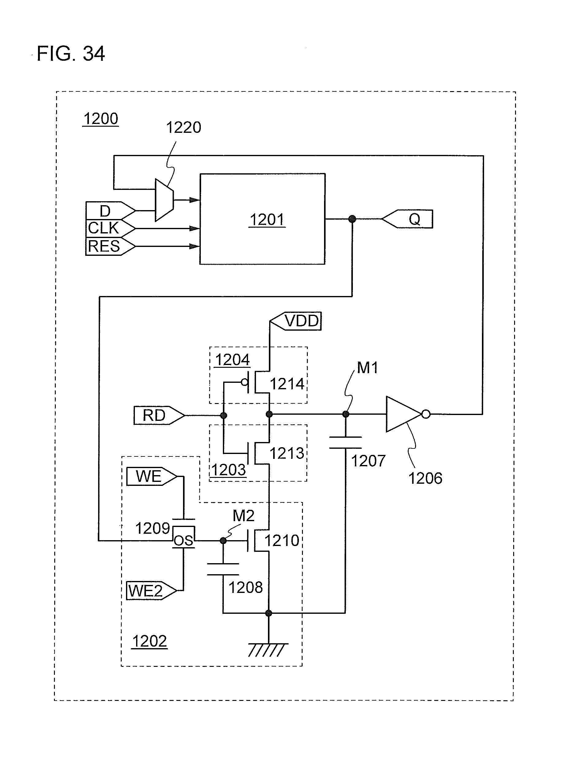
D00035

D00036

D00037

D00038

D00039

D00040

D00041

D00042

D00043

D00044

XML
uspto.report is an independent third-party trademark research tool that is not affiliated, endorsed, or sponsored by the United States Patent and Trademark Office (USPTO) or any other governmental organization. The information provided by uspto.report is based on publicly available data at the time of writing and is intended for informational purposes only.
While we strive to provide accurate and up-to-date information, we do not guarantee the accuracy, completeness, reliability, or suitability of the information displayed on this site. The use of this site is at your own risk. Any reliance you place on such information is therefore strictly at your own risk.
All official trademark data, including owner information, should be verified by visiting the official USPTO website at www.uspto.gov. This site is not intended to replace professional legal advice and should not be used as a substitute for consulting with a legal professional who is knowledgeable about trademark law.