Arrangements for magnetic field sensors to cancel offset variations
David , et al.
U.S. patent number 10,260,905 [Application Number 15/176,655] was granted by the patent office on 2019-04-16 for arrangements for magnetic field sensors to cancel offset variations. This patent grant is currently assigned to Allegro MicroSystems, LLC. The grantee listed for this patent is Allegro MicroSystems, LLC. Invention is credited to Paul A. David, Jeffrey Eagen, Eric G. Shoemaker.


View All Diagrams
| United States Patent | 10,260,905 |
| David , et al. | April 16, 2019 |
| **Please see images for: ( Certificate of Correction ) ** |
Arrangements for magnetic field sensors to cancel offset variations
Abstract
A magnetic field sensor can sense a movement of an object along a path. A movement line is tangent to the path. The magnetic field sensor can include a semiconductor substrate. The semiconductor substrate can have first and second orthogonal axes orthogonal to each other on the first surface of the substrate. A projection of the movement line onto a surface of the semiconductor substrate is only substantially parallel to the first orthogonal axis. The magnetic field sensor can also include first, second, third, and fourth magnetic field sensing elements disposed on the substrate. The first and second magnetic field sensing elements have maximum response axes parallel to the first orthogonal axis and the second and fourth magnetic field sensing elements have maximum response axes parallel to the second orthogonal axis. Signals generated by the second and fourth magnetic field sensing elements can be used as reference signals.
| Inventors: | David; Paul A. (Bow, NH), Shoemaker; Eric G. (Windham, NH), Eagen; Jeffrey (Manchester, NH) | ||||||||||
|---|---|---|---|---|---|---|---|---|---|---|---|
| Applicant: |
|
||||||||||
| Assignee: | Allegro MicroSystems, LLC
(Manchester, NH) |
||||||||||
| Family ID: | 58800939 | ||||||||||
| Appl. No.: | 15/176,655 | ||||||||||
| Filed: | June 8, 2016 |
Prior Publication Data
| Document Identifier | Publication Date | |
|---|---|---|
| US 20170356760 A1 | Dec 14, 2017 | |
| Current U.S. Class: | 1/1 |
| Current CPC Class: | G01D 5/142 (20130101); G01D 5/16 (20130101); G01D 5/147 (20130101) |
| Current International Class: | G01D 5/14 (20060101); G01D 5/16 (20060101) |
| Field of Search: | ;324/207.11,207.24,207.25,207.26,207.2,207.21,207.22,3,207.23 |
References Cited [Referenced By]
U.S. Patent Documents
| 3195043 | July 1965 | Burig et al. |
| 3281628 | October 1966 | Bauer et al. |
| 3607528 | September 1971 | Gassaway |
| 3661061 | May 1972 | Tokarz |
| 3728786 | April 1973 | Lucas et al. |
| 4048670 | September 1977 | Eysermans |
| 4079360 | March 1978 | Ookubo et al. |
| 4188605 | February 1980 | Stout |
| 4204317 | May 1980 | Winn |
| 4236832 | December 1980 | Komatsu et al. |
| 4283643 | August 1981 | Levin |
| 4315523 | February 1982 | Mahawili et al. |
| 4438347 | March 1984 | Gehring |
| 4573258 | March 1986 | Io et al. |
| 4614111 | September 1986 | Wolff |
| 4649796 | March 1987 | Schmidt |
| 4670715 | June 1987 | Fuzzell |
| 4719419 | January 1988 | Dawley |
| 4733455 | March 1988 | Nakamura et al. |
| 4745363 | May 1988 | Carr et al. |
| 4746859 | May 1988 | Malik |
| 4752733 | June 1988 | Petr et al. |
| 4758943 | July 1988 | Astrom et al. |
| 4760285 | July 1988 | Nelson |
| 4769344 | September 1988 | Sakai et al. |
| 4772929 | September 1988 | Manchester |
| 4789826 | December 1988 | Willett |
| 4796354 | January 1989 | Yokoyama et al. |
| 4823075 | April 1989 | Alley |
| 4833406 | May 1989 | Foster |
| 4893027 | January 1990 | Kammerer et al. |
| 4908685 | March 1990 | Shibasaki et al. |
| 4910861 | March 1990 | Dohogne |
| 4935698 | June 1990 | Kawaji et al. |
| 4970411 | November 1990 | Halg et al. |
| 4983916 | January 1991 | Iijima et al. |
| 5012322 | April 1991 | Guillotte |
| 5021493 | June 1991 | Sandstrom |
| 5028868 | July 1991 | Murata et al. |
| 5038130 | August 1991 | Eck et al. |
| 5045920 | September 1991 | Vig |
| 5078944 | January 1992 | Yoshino |
| 5084289 | January 1992 | Shin et al. |
| 5121289 | June 1992 | Gagliardi |
| 5137677 | August 1992 | Murata |
| 5139973 | August 1992 | Nagy et al. |
| 5167896 | December 1992 | Hirota et al. |
| 5168244 | December 1992 | Muranaka |
| 5185919 | February 1993 | Hickey |
| 5196794 | March 1993 | Murata |
| 5210493 | May 1993 | Schroeder et al. |
| 5216405 | June 1993 | Schroeder et al. |
| 5244834 | September 1993 | Suzuki et al. |
| 5247202 | September 1993 | Popovic et al. |
| 5247278 | September 1993 | Pant et al. |
| 5250925 | October 1993 | Shinkle |
| 5286426 | February 1994 | Rano, Jr. et al. |
| 5289344 | February 1994 | Gagnon et al. |
| 5304926 | April 1994 | Wu |
| 5315245 | May 1994 | Schroeder et al. |
| 5329416 | July 1994 | Ushiyama et al. |
| 5331478 | July 1994 | Aranovsky |
| 5332956 | July 1994 | Oh |
| 5332965 | July 1994 | Wolf et al. |
| 5341097 | August 1994 | Wu |
| 5359287 | October 1994 | Watanabe |
| 5412255 | May 1995 | Wallrafen |
| 5414355 | May 1995 | Davidson et al. |
| 5424558 | June 1995 | Borden et al. |
| 5434105 | July 1995 | Liou |
| 5453727 | September 1995 | Shibasaki et al. |
| 5469058 | November 1995 | Dunnam |
| 5477143 | December 1995 | Wu |
| 5479695 | January 1996 | Grader et al. |
| 5486759 | January 1996 | Seiler et al. |
| 5488294 | January 1996 | Liddell et al. |
| 5491633 | February 1996 | Henry et al. |
| 5497081 | March 1996 | Wolf et al. |
| 5500589 | March 1996 | Sumcad |
| 5500994 | March 1996 | Itaya |
| 5508611 | April 1996 | Schroeder et al. |
| 5521501 | May 1996 | Dettmann et al. |
| 5545983 | August 1996 | Okeya et al. |
| 5551146 | September 1996 | Kawabata et al. |
| 5581170 | December 1996 | Mammano et al. |
| 5581179 | December 1996 | Engel et al. |
| 5596272 | January 1997 | Busch |
| 5621319 | April 1997 | Bilotti et al. |
| 5627315 | May 1997 | Figi et al. |
| 5631557 | May 1997 | Davidson |
| 5640090 | June 1997 | Furuya et al. |
| 5691637 | November 1997 | Oswald et al. |
| 5696790 | December 1997 | Graham et al. |
| 5712562 | January 1998 | Berg |
| 5714102 | February 1998 | Highum et al. |
| 5719496 | February 1998 | Wolf |
| 5729128 | March 1998 | Bunyer et al. |
| 5757181 | May 1998 | Wolf et al. |
| 5781005 | July 1998 | Vig et al. |
| 5789658 | August 1998 | Henn et al. |
| 5789915 | August 1998 | Ingraham |
| 5796249 | August 1998 | Andraet et al. |
| 5818222 | October 1998 | Ramsden |
| 5818223 | October 1998 | Wolf |
| 5839185 | November 1998 | Smith et al. |
| 5841276 | November 1998 | Makino et al. |
| 5859387 | January 1999 | Gagnon |
| 5883567 | March 1999 | Mullins, Jr. |
| 5886070 | March 1999 | Honkura et al. |
| 5912556 | June 1999 | Frazee et al. |
| 5963028 | October 1999 | Engel et al. |
| 6011770 | January 2000 | Tan |
| 6016055 | January 2000 | Jager et al. |
| 6043646 | March 2000 | Jansseune |
| 6136250 | October 2000 | Brown |
| 6169396 | January 2001 | Yokotani et al. |
| 6175233 | January 2001 | McCurley et al. |
| 6180041 | January 2001 | Takizawa |
| 6184679 | February 2001 | Popovic et al. |
| 6194893 | February 2001 | Yokotani et al. |
| 6198373 | March 2001 | Ogawa et al. |
| 6242604 | June 2001 | Hudlicky et al. |
| 6242904 | June 2001 | Shirai et al. |
| 6242905 | June 2001 | Draxelmayr |
| 6265865 | July 2001 | Engel et al. |
| 6278269 | August 2001 | Vig et al. |
| 6291989 | September 2001 | Schroeder |
| 6297627 | October 2001 | Towne et al. |
| 6297628 | October 2001 | Bicking et al. |
| 6323642 | November 2001 | Nishimura et al. |
| 6339322 | January 2002 | Loreck et al. |
| 6351506 | February 2002 | Lewicki |
| 6356068 | March 2002 | Steiner et al. |
| 6392478 | May 2002 | Mulder et al. |
| 6436748 | August 2002 | Forbes et al. |
| 6437558 | August 2002 | Li et al. |
| 6452381 | September 2002 | Nakatani et al. |
| 6492804 | December 2002 | Tsuge et al. |
| 6501270 | December 2002 | Opie |
| 6525531 | February 2003 | Forrest et al. |
| 6528992 | March 2003 | Shinjo et al. |
| 6542847 | April 2003 | Lohberg et al. |
| 6545332 | April 2003 | Huang |
| 6545457 | April 2003 | Goto et al. |
| 6545462 | April 2003 | Schott et al. |
| 6590804 | July 2003 | Perner |
| 6653968 | November 2003 | Schneider |
| 6674679 | January 2004 | Perner et al. |
| 6687644 | February 2004 | Zinke et al. |
| 6692676 | February 2004 | Vig et al. |
| 6768301 | July 2004 | Hohe |
| 6770163 | August 2004 | Kuah et al. |
| 6781233 | August 2004 | Zverev et al. |
| 6781359 | August 2004 | Stauth et al. |
| 6798193 | September 2004 | Zimmerman et al. |
| 6815944 | November 2004 | Vig et al. |
| 6822443 | November 2004 | Dogaru |
| 6853178 | February 2005 | Hayat-Dawoodi |
| 6896407 | May 2005 | Nomiyama et al. |
| 6902951 | June 2005 | Goller et al. |
| 6917321 | July 2005 | Haurie et al. |
| 7023205 | April 2006 | Krupp |
| 7026808 | April 2006 | Vig et al. |
| 7031170 | April 2006 | Daeche et al. |
| 7038448 | May 2006 | Schott et al. |
| 7112955 | September 2006 | Buchhold |
| 7112957 | September 2006 | Bicking |
| 7126327 | October 2006 | Busch |
| 7184876 | February 2007 | Teulings et al. |
| 7190784 | March 2007 | Li |
| 7193412 | March 2007 | Freeman |
| 7199579 | April 2007 | Scheller et al. |
| 7253614 | August 2007 | Forrest et al. |
| 7259545 | August 2007 | Stauth et al. |
| 7265531 | September 2007 | Stauth et al. |
| 7269992 | September 2007 | Lamb et al. |
| 7285952 | October 2007 | Hatanaka et al. |
| 7292095 | November 2007 | Burt et al. |
| 7295000 | November 2007 | Werth |
| 7319319 | January 2008 | Jones et al. |
| 7323780 | January 2008 | Daubenspeck et al. |
| 7323870 | January 2008 | Tatschl et al. |
| 7325175 | January 2008 | Momtaz |
| 7345468 | March 2008 | Okada et al. |
| 7355388 | April 2008 | Ishio |
| 7361531 | April 2008 | Sharma et al. |
| 7362094 | April 2008 | Voisine et al. |
| 7365530 | April 2008 | Bailey et al. |
| 7368904 | May 2008 | Scheller et al. |
| 7385394 | June 2008 | Auburger et al. |
| 7425821 | September 2008 | Monreal et al. |
| 7474093 | January 2009 | Ausserlechner |
| 7476953 | January 2009 | Taylor et al. |
| 7518354 | April 2009 | Stauth et al. |
| 7592801 | September 2009 | Bailey et al. |
| 7598601 | October 2009 | Taylor et al. |
| 7605647 | October 2009 | Romero et al. |
| 7635993 | December 2009 | Boeve |
| 7694200 | April 2010 | Forrest et al. |
| 7701208 | April 2010 | Nishikawa |
| 7729675 | June 2010 | Krone |
| 7746056 | June 2010 | Stauth et al. |
| 7746065 | June 2010 | Pastre et al. |
| 7764118 | July 2010 | Kusuda et al. |
| 7768083 | August 2010 | Doogue et al. |
| 7769110 | August 2010 | Momtaz |
| 7772838 | August 2010 | Bailey et al. |
| 7800389 | September 2010 | Friedrich et al. |
| 7808074 | October 2010 | Knittl |
| 7816772 | October 2010 | Engel et al. |
| 7816905 | October 2010 | Doogue et al. |
| 7839141 | November 2010 | Werth et al. |
| 7915886 | March 2011 | Stolfus |
| 7923996 | April 2011 | Doogue et al. |
| 7936144 | May 2011 | Vig et al. |
| 7956604 | June 2011 | Ausserlechner |
| 7961823 | June 2011 | Kolze et al. |
| 7990209 | August 2011 | Romero |
| 8030918 | October 2011 | Doogue et al. |
| 8058870 | November 2011 | Sterling |
| 8063634 | November 2011 | Sauber et al. |
| 8080993 | December 2011 | Theuss et al. |
| 8089276 | January 2012 | Kentsch |
| 8106654 | January 2012 | Theuss et al. |
| 8128549 | March 2012 | Testani et al. |
| 8134358 | March 2012 | Charlier et al. |
| 8143169 | March 2012 | Engel et al. |
| 8253210 | August 2012 | Theuss et al. |
| 8362579 | January 2013 | Theuss et al. |
| 8610430 | December 2013 | Werth et al. |
| 8624588 | January 2014 | Vig et al. |
| 8729890 | May 2014 | Donovan et al. |
| 8773124 | July 2014 | Ausserlechner |
| 9116018 | August 2015 | Frachon |
| 9164156 | October 2015 | Elian et al. |
| 9201123 | December 2015 | Elian et al. |
| 9347799 | May 2016 | Nazarian et al. |
| 2001/0002791 | June 2001 | Tsuge et al. |
| 2001/0009367 | July 2001 | Seitzer et al. |
| 2002/0027488 | March 2002 | Hayat-Dawoodi et al. |
| 2002/0084923 | July 2002 | Li |
| 2003/0001563 | January 2003 | Turner |
| 2003/0038675 | February 2003 | Gailus et al. |
| 2003/0062891 | April 2003 | Slates |
| 2003/0102909 | June 2003 | Motz |
| 2003/0107366 | June 2003 | Busch et al. |
| 2003/0173955 | September 2003 | Uenoyama |
| 2004/0032251 | February 2004 | Zimmerman et al. |
| 2004/0046248 | March 2004 | Waelti et al. |
| 2004/0062362 | April 2004 | Matsuya |
| 2004/0080314 | April 2004 | Tsujii et al. |
| 2004/0135220 | July 2004 | Goto |
| 2004/0155647 | August 2004 | Stauth et al. |
| 2004/0174164 | September 2004 | Ao |
| 2004/0184196 | September 2004 | Jayasekara |
| 2004/0189285 | September 2004 | Uenoyama |
| 2004/0252563 | December 2004 | Hckuto et al. |
| 2005/0120782 | June 2005 | Kishibata et al. |
| 2005/0167790 | August 2005 | Khor et al. |
| 2005/0179429 | August 2005 | Lohberg |
| 2005/0225318 | October 2005 | Bailey et al. |
| 2005/0258820 | November 2005 | Forster |
| 2005/0280411 | December 2005 | Bicking |
| 2006/0033487 | February 2006 | Nagano et al. |
| 2006/0038559 | February 2006 | Lamb et al. |
| 2006/0068237 | March 2006 | Murphy |
| 2006/0125473 | June 2006 | Frachon et al. |
| 2006/0175674 | August 2006 | Taylor |
| 2006/0181263 | August 2006 | Doogue et al. |
| 2006/0202692 | September 2006 | Tatschl et al. |
| 2006/0238190 | October 2006 | Ishio |
| 2006/0261801 | November 2006 | Busch |
| 2007/0110199 | May 2007 | Momtaz et al. |
| 2007/0247141 | October 2007 | Pastre et al. |
| 2007/0285089 | December 2007 | Ibuki et al. |
| 2008/0012558 | January 2008 | Rossler et al. |
| 2008/0013298 | January 2008 | Sharma et al. |
| 2008/0094055 | April 2008 | Monreal et al. |
| 2008/0116884 | May 2008 | Rettig et al. |
| 2008/0137784 | June 2008 | Krone |
| 2008/0237818 | October 2008 | Engel et al. |
| 2008/0238410 | October 2008 | Charlier et al. |
| 2009/0001964 | January 2009 | Strzalkowski |
| 2009/0001972 | January 2009 | Fernandez et al. |
| 2009/0058404 | March 2009 | Kurumado |
| 2009/0085706 | April 2009 | Baarman et al. |
| 2009/0102467 | April 2009 | Snell et al. |
| 2009/0140725 | June 2009 | Ausserlechner |
| 2009/0146647 | June 2009 | Ausserlechner |
| 2009/0152696 | June 2009 | Dimasacat et al. |
| 2009/0206827 | August 2009 | Aimuta et al. |
| 2009/0212765 | August 2009 | Doogue et al. |
| 2009/0315543 | December 2009 | Guo et al. |
| 2010/0026279 | February 2010 | Vig et al. |
| 2010/0045268 | February 2010 | Kilian |
| 2010/0072988 | March 2010 | Hammerschmidt et al. |
| 2010/0141249 | June 2010 | Ararao et al. |
| 2010/0188078 | July 2010 | Foletto et al. |
| 2010/0201356 | August 2010 | Koller et al. |
| 2010/0211347 | August 2010 | Friedrich et al. |
| 2010/0237450 | September 2010 | Doogue et al. |
| 2010/0276769 | November 2010 | Theuss et al. |
| 2010/0295140 | November 2010 | Theuss et al. |
| 2010/0330708 | December 2010 | Engel et al. |
| 2011/0018533 | January 2011 | Cesaretti et al. |
| 2011/0031960 | February 2011 | Hohe et al. |
| 2011/0048102 | March 2011 | Fernandez et al. |
| 2011/0074405 | March 2011 | Doogue et al. |
| 2011/0127998 | June 2011 | Elian et al. |
| 2011/0267040 | November 2011 | Frachon |
| 2011/0298448 | December 2011 | Foletto et al. |
| 2012/0007589 | January 2012 | Okada |
| 2012/0013333 | January 2012 | Ararao et al. |
| 2012/0019236 | January 2012 | Tiernan et al. |
| 2012/0086090 | April 2012 | Sharma et al. |
| 2012/0249133 | October 2012 | Friedrich |
| 2012/0274314 | November 2012 | Cesaretti et al. |
| 2013/0016845 | January 2013 | Fox |
| 2013/0113474 | May 2013 | Elian |
| 2013/0214774 | August 2013 | Cesaretti et al. |
| 2013/0278246 | October 2013 | Stegerer et al. |
| 2013/0335069 | December 2013 | Vig et al. |
| 2014/0084906 | March 2014 | Ruigrok et al. |
| 2014/0175584 | June 2014 | Foletto et al. |
| 2014/0176126 | June 2014 | Friedrich et al. |
| 2014/0266176 | September 2014 | Fernandez et al. |
| 2015/0022186 | January 2015 | Ausserlechner |
| 2015/0022187 | January 2015 | Taylor et al. |
| 2015/0377648 | December 2015 | Sirohiwala |
| 2016/0025820 | January 2016 | Scheller et al. |
| 2016/0123774 | May 2016 | Foletto et al. |
| 683 469 | Mar 1994 | CH | |||
| 25 18 054 | Nov 1976 | DE | |||
| 40 31 560 | Apr 1992 | DE | |||
| 195 39 458 | Apr 1997 | DE | |||
| 196 34 715 | Mar 1998 | DE | |||
| 196 50 935 | Jun 1998 | DE | |||
| 198 38 433 | Mar 1999 | DE | |||
| 19851839 | Nov 1999 | DE | |||
| 199 61 504 | Jun 2001 | DE | |||
| 102 10 184 | Sep 2003 | DE | |||
| 103 14 602 | Oct 2004 | DE | |||
| 10 2004017191 | Oct 2005 | DE | |||
| 10 2006 037 226 | Feb 2008 | DE | |||
| 10 2007 018 238 | Oct 2008 | DE | |||
| 10 2007 041 230 | Apr 2009 | DE | |||
| 10 2010 016 584 | Nov 2010 | DE | |||
| 10 2011 102483 | Nov 2012 | DE | |||
| 0 289 414 | Nov 1988 | EP | |||
| 0 289 414 | Nov 1988 | EP | |||
| 0 357 013 | Mar 1990 | EP | |||
| 0 357 013 | Mar 1990 | EP | |||
| 0 361 456 | Apr 1990 | EP | |||
| 0 361 456 | Apr 1990 | EP | |||
| 0 504 583 | Sep 1992 | EP | |||
| 0629634 | Dec 1994 | EP | |||
| 0 680 103 | Nov 1995 | EP | |||
| 0 898 180 | Feb 1999 | EP | |||
| 0 944 888 | Oct 2001 | EP | |||
| 1 443 332 | Aug 2004 | EP | |||
| 1 580 560 | Sep 2005 | EP | |||
| 1 637 898 | Mar 2006 | EP | |||
| 1 662 353 | May 2006 | EP | |||
| 1 679 524 | Jul 2006 | EP | |||
| 1 850 143 | Oct 2007 | EP | |||
| 2 063 229 | May 2009 | EP | |||
| 2402719 | Jan 2012 | EP | |||
| 2 730 893 | May 2014 | EP | |||
| 2 748 105 | Oct 1997 | FR | |||
| 2 909 756 | Jun 2008 | FR | |||
| 2276727 | Oct 1994 | GB | |||
| 2481482 | Dec 2011 | GB | |||
| 61-43777 | Mar 1986 | JP | |||
| 363 084176 | Apr 1988 | JP | |||
| 63-263782 | Oct 1988 | JP | |||
| 63-300911 | Dec 1988 | JP | |||
| H02-116753 | May 1990 | JP | |||
| 02-149013 | Jun 1990 | JP | |||
| H03-29817 | Feb 1991 | JP | |||
| 04-152688 | May 1992 | JP | |||
| H06-273437 | Sep 1994 | JP | |||
| 08-97486 | Apr 1996 | JP | |||
| 09-166612 | Jun 1997 | JP | |||
| H 1038988 | Feb 1998 | JP | |||
| 10-332725 | Dec 1998 | JP | |||
| H 10318784 | Dec 1998 | JP | |||
| 11-74142 | Mar 1999 | JP | |||
| 11-084363 | Mar 1999 | JP | |||
| 2000-183241 | Jun 2000 | JP | |||
| 2001-043475 | Feb 2001 | JP | |||
| 2001-141738 | May 2001 | JP | |||
| 2001-165702 | Jun 2001 | JP | |||
| 2001-1659951 | Jun 2001 | JP | |||
| 2002-117500 | Apr 2002 | JP | |||
| 2002-149013 | May 2002 | JP | |||
| 2002-357920 | Dec 2002 | JP | |||
| 2003-177171 | Jun 2003 | JP | |||
| 2004-055932 | Feb 2004 | JP | |||
| 2004-093381 | Mar 2004 | JP | |||
| 2004-152688 | May 2004 | JP | |||
| 2004-356338 | Dec 2004 | JP | |||
| 2004-357858 | Dec 2004 | JP | |||
| 2005-517928 | Jun 2005 | JP | |||
| 2005-337866 | Dec 2005 | JP | |||
| 2005-345302 | Dec 2005 | JP | |||
| 2006-003096 | Jan 2006 | JP | |||
| 2007-012582 | Jan 2007 | JP | |||
| 2007-218799 | Aug 2007 | JP | |||
| 2008-264569 | Nov 2008 | JP | |||
| WO 88/09026 | Nov 1988 | WO | |||
| WO 93/12403 | Jun 1993 | WO | |||
| WO 1993/12403 | Jun 1993 | WO | |||
| WO 94/08203 | Apr 1994 | WO | |||
| WO 1994/08203 | Apr 1994 | WO | |||
| WO 95/18982 | Jul 1995 | WO | |||
| WO 1995/18982 | Jul 1995 | WO | |||
| WO 98/02849 | Feb 1996 | WO | |||
| WO 1999/49322 | Sep 1999 | WO | |||
| WO 2001/74139 | Oct 2001 | WO | |||
| WO 2001/74139 | Oct 2001 | WO | |||
| WO 2003/069358 | Aug 2003 | WO | |||
| WO 2003/069358 | Aug 2003 | WO | |||
| WO 2003/107018 | Dec 2003 | WO | |||
| WO 2004/027436 | Apr 2004 | WO | |||
| WO 2004/072672 | Aug 2004 | WO | |||
| WO 2005/013363 | Feb 2005 | WO | |||
| WO 2005/013363 | Feb 2005 | WO | |||
| WO 2006/056829 | Jun 2006 | WO | |||
| WO 2006/083479 | Aug 2006 | WO | |||
| WO 2007/138508 | Dec 2007 | WO | |||
| WO 2008/008140 | Jan 2008 | WO | |||
| WO 2008/008140 | Jan 2008 | WO | |||
| WO 2008/048379 | Apr 2008 | WO | |||
| WO 2008/121443 | Oct 2008 | WO | |||
| WO 2008/145662 | Dec 2008 | WO | |||
| WO 2009/108422 | Sep 2009 | WO | |||
| WO 2009/108422 | Sep 2009 | WO | |||
| WO 2010/014309 | Feb 2010 | WO | |||
| WO 2010/065315 | Jun 2010 | WO | |||
| WO 2010/096367 | Aug 2010 | WO | |||
| WO 2011/011479 | Jan 2011 | WO | |||
| WO 2012/148646 | Nov 2012 | WO | |||
| WO 2013/169455 | Nov 2013 | WO | |||
Other References
|
Office Action dated Aug. 26, 2016 for U.S. Appl. No. 13/946,380, 40 pages. cited by applicant . Response filed on Nov. 9, 2016 to the Non-Final Office Action dated Aug. 26, 2016; for U.S. Appl. No. 13/946,380; 19 pages. cited by applicant . Response to Office Action filed on Nov. 9, 2016 for U.S. Appl. No. 13/946,380; 19 pages. cited by applicant . EP Response filed on Dec. 9, 2016 to Official Communication dated Oct. 14, 2016 regarding European Pat. Appl. No. 14742067.3; 23 pages. cited by applicant . Final Office Action dated Jan. 12, 2017 for U.S. Appl. No. 13/946,380; 32 pages. cited by applicant . European Search Report dated Apr. 5, 2017 for EP Pat. Appl. No. 16192498.0: 10 pages. cited by applicant . Request for Continued Examination filed on Apr. 11, 2017 for U.S. Appl. No. 13/946,380; 3 pages. cited by applicant . Amendment filed on Apr. 11, 2017 for U.S. Appl. No. 13/946,380; 18 pages. cited by applicant . Office Action dated May 19, 2017 for U.S. Appl. No. 13/946,380; 20 pages. cited by applicant . Response to Office Action filed on Jun. 22, 2017 for U.S. Appl. No. 13/946,380; 8 pages. cited by applicant . Notice of Allowance dated Jul. 13, 2017 for U.S. Appl. No. 13/946,380; 11 pages. cited by applicant . PCT Search Report and Written Opinion dated Jul. 31, 2017 for PCT Application PCT/US2017/033057; 11 pages. cited by applicant . Response to Notice to File Corrected Application Papers dated Aug. 28, 2017 and flied on Aug. 29, 2017 for U.S. Appl. No. 13/946,380; 3 pages. cited by applicant . U.S. Appl. No. 13/439,094, filed Apr. 4, 2012, Friedrich et al. cited by applicant . U.S. Appl. No. 13/748,999, filed Jan. 24, 2013, Vig et al. cited by applicant . U.S. Appl. No. 13/871,131, filed Apr. 26, 2013, David et al. cited by applicant . U.S. Appl. No. 15/176,665, filed Jun. 8, 2016, Vig et al. cited by applicant . Kapser et al.; "Integrated GMR Based Wheel Speed Sensor for Automotive Applications;" IEEE 2007 Conference on Sensors; Oct. 2007; pp. 848-851. cited by applicant . Oniku et al.; "High-Energy-Density Permanent Micromagnets Formed From Heterogeneous Magnetic Powder Mixtures;" IEEE 25.sup.th International Conference on Micro Electro Mechanical Systmes, Jan. 2012; 4 pages. cited by applicant . Office Action dated Jul. 9, 2015; for U.S. Appl. No. 13/946,380; 63 pages. cited by applicant . Response filed Nov. 9, 2015; to Office Action dated Jul. 9, 2015; for U.S. Appl. No. 13/946,380; 26 pages. cited by applicant . Final Office Action dated Dec. 15, 2015; for U.S. Appl. No. 13/946,380; 36 pages. cited by applicant . Response to Final Office Action filed on Apr. 12, 2016, dated Dec. 15, 2015; for U.S. Appl. No. 13/946,380; 17 pages. cited by applicant . Request for Continued Examination filed Apr. 12, 2015; for U.S. Appl. No. 13/946,380; 2 pages. cited by applicant . Office Action dated Jul. 23, 2016 for U.S. Appl. No. 14/529,669; 78 pages. cited by applicant . Office Action dated Jul. 14, 2016 for U.S. Appl. No, 14/529,594; 94 pages. cited by applicant . PCT Invitation to Pay Additional Fees and Partial Search Report dated Nov. 4, 2014; for PCT Pat. App. No. PCT/US2014/044236; 6 pages. cited by applicant . PCT International Preliminary Report on Patentability and Written Opinion of the ISA dated Jan. 28, 2016; for PCT Pat. App. No. PCT/US2014/044236; 17 pages. cited by applicant . PCT International Search Report and Written Opinion of the ISA dated Jan. 15, 2016; for PCT Pat. App. No. PCT/US2015/055236; 12 pages. cited by applicant . PCT International Search Report and Written Opinion of the ISA dated Dec. 23, 2015; for PCT Pat. App. No. PCT/US2015/055233; 12 pages. cited by applicant . PCT International Search Report and Written Opinion of the ISA dated Aug. 3, 2018; for PCT Application No. PCT/US2015/055230; 12 pages. cited by applicant . PCT International Search Report and Written Opinion of the ISA dated Feb. 4 2016; for PCT Pat. App. No. PCT/US2015/055474; 15 pages. cited by applicant . U.S. Appl. No. 13/946,010, filed Jul. 19, 2013, David et al. cited by applicant . U.S. Appl. No. 13/946,400, filed Jul. 19, 2013, David et al. cited by applicant . U.S. Appl. No. 13/946,417, filed Jul. 19, 2013, Burdette et al. cited by applicant . U.S. Appl. No. 13/946,830, filed Jul. 19, 2013, Taylor et al. cited by applicant . U.S. Appl. No. 14/529,577, filed Oct. 31, 2014, Foletto et al. cited by applicant . U.S. Appl. No. 14/529,594, filed Oct. 31, 2014, Drouin et al. cited by applicant . U.S. Appl. No. 14/529,606, filed Oct. 31, 2014, Foletto et al. cited by applicant . U.S. Appl. No. 14/529,669, filed Oct. 31, 2014, David et al. cited by applicant . Office Action in U.S. appl. No. 13/468,478 dated Jan. 15, 2014, 36 pages. cited by applicant . International Search Report and Written Opinion dated Oct. 28, 2014 for Int'l PCT Application PCT/US2014/044991; 12 pages. cited by applicant . International Search Report and Written Opinion dated Nov. 4, 2014 for Int'l PCT Application PCT/US2014/044993; 13 pages. cited by applicant . PCT Search Report and Written Opinion of the ISA dated Dec. 19, 2014; for PCT Pat. App. No. PCT/US2014/044236; 23 pages. cited by applicant . U.S. Appl. No. 12/840,324, filed Jul. 21, 2010, Casaretti et al. cited by applicant . U.S. Appl. No. 12/959,672, filed Dec. 3, 2010, Doogue et al. cited by applicant . U.S. Appl. No. 12/968,353, filed Dec. 15, 2010, Donovan et al. cited by applicant . U.S. Appl. No. 13/095,371, filed Apr. 27, 2011, Cesaretti et al. cited by applicant . U.S. Appl. No. 13/350,970, filed Jan. 16, 2012, Milano et al. cited by applicant . U.S. Appl. No. 13/398,127, filed Feb. 16, 2012, Cesaretti et al. cited by applicant . U.S. Appl. No. 13/424,618, filed Apr. 20, 2012, Doogue et al. cited by applicant . U.S. Appl. No. 13/526,106, filed Jun. 18, 2013, Vig et al. cited by applicant . Ahn et al., "A New Toroidal-Meander Type Integrated Inductor With A Multilevel Meander Magnetic Core", IEEE Transactions on Magnetics, vol. 30, No. 1, Jan. 1994, pp. 73-79. cited by applicant . Allegro "Two-Wire True Zero Speed Miniature Differential Peak-Detecting Gear Tooth Sensor;" ATS646LSH; 2004; Allegro MicroSystems, Inc., Worcester, MA 01615; pp. 1-14. cited by applicant . Allegro Microsystems, Inc. Data Sheet A1341; "High Precision, Highly Programmable Linear Hall Effect Sensor IC with EEPROM, Output Protocols SENT and PWM, an Advanced Output Linearization Capabilities;" May 17, 2010; 46 pages. cited by applicant . Allegro Microsystems, Inc. Data Sheet ATS601LSG; "Non-TPOS, Tooth Detecting Speed Sensor;" Nov. 1, 2011; 9 pages. cited by applicant . Allegro Microsystems, Inc., "Gear-Tooth Sensor for Automotive Applications," Aug. 3, 2001. cited by applicant . Allegro MicroSystems, Inc., Hall-Effect IC Applications Guide, http://www.allegromicro.com/en/Products/Design/an/an27701.pdf, Copyright 1987, 1997, pp. 1-36. cited by applicant . Alllegro "True Zero-Speed Low-Jitter High Accuracy Gear Tooth Sensor;" ATS825LSG; 2005; Allegro McroSystems, Inc. Worcester, MA 01615; pp. 1-21. cited by applicant . Ausserlechner et al.; "Compensation of the Piezo-Hall Effect in Integrated Hall Sensors on (100)-Si;" Sensors Journal, vol. 7, No. 11; Nov. 2007; ISBN: 1530-437X; pp. 1475-1482. cited by applicant . Ausserlechner et al.; "Drift of Magnetic Sensitivity of Small Hall Sensors Due to Moisture Absorbed by the IC-Package;" Proceedings of IEEE Sensors, 2004; vol. 1; Oct. 24, 2004; ISBN:0-7803-8692-2; pp. 455-458. cited by applicant . Ausserlechner; "Limits of Offset Cancellation by the Principle of Spinning Current Hall Probe;" Proceedings of IEEE Sensors; Oct. 2004; pp. 1117-1120. cited by applicant . Ausserlechner; "The piezo-Hall effect in n-silicon for arbitrary crystal orientaton;" Proceedings of IEEE Sensors; vol. 3; Oct. 24, 2004; ISBN: 0-7803-8692-2; pp. 1149-1152. cited by applicant . Bahreyni, et al.; "A Resonant Micromachined Magnetic Field Sensor;" IEEE Sensors Journal; vol. 7, No. 9, Sep. 2007; pp. 1326-1334. cited by applicant . Barrettino, et al.; "CMOS-Based Monolithis Controllers for Smart Sensors Comprising Micromembranes and Microcantilevers;" IEEE Transactions on Circuits and System-I Regular Papers vol. 54, No. 1; Jan. 2007; pp. 141-152. cited by applicant . Baschirotto et al.; "Development and Anaiysis of PCB Vector 2-D Magnetic Field Sensor System for Electronic Compass;" IEEE Sensors Journal vol. 6, No. 2; Apr. 2006; pp. 365-371. cited by applicant . Bilotti et al.; "Monolithic Magnetic Hall Sensor Using Dynamic Quardrature Offset Cancellation," IEEE Journal of Solid-State Circuits; vol. 32, Issue 6; Jun. 1997; pp. 829-835. cited by applicant . Bowers et al., "Microfabrication and Process Integration of Powder-Based Permanent Magnets", Interdisciplinary Microsystems Group, Dept. Eiectrical and Computer Engineering, University of Florida, USA; Technologies for Future Micro-Nano Manufacturing Workshop, Napa, California, Aug. 8-10, 2011, pp. 162-165. cited by applicant . Demierre, et al.; "Reference Magnetic Actuator for Self-Calibration of a Very Small Hall Sensor Array;" Sensors and Actuators A97-98; Apr. 2002; pp. 39-46. cited by applicant . Dwyer, "Back-Biased Packaging Advances (SE, SG & SH versus SA & SB)," http://www.allegromicro.com/en/Products/Design/packaging_advances/index.a- sp, Copyright 2008, pp. 1-5. cited by applicant . Frick, et al.; "CMOS Microsystem for AC Current Measurement with Galvanic Isolation;" IEEE Sensors Journal; vol. 3, No. 6; Dec. 2003; pp. 752-760. cited by applicant . Halg; "Piezo-Hall Coefficients of n-Type Silicon;" Journal of Applied Physics; vol. 84, No. 1; Jul. 1, 1988; pp. 276-282. cited by applicant . Honeywell International, Inc., "Hall Effect Sensing and Application," Micro Switch Sensing and Control, Chapter 3, http://content.honeywell.com/sensing/prodinfo/solidstate/technical/hallbo- ok.pdf, date unavailable but believed to be before Jan. 2008, pp. 9-18. cited by applicant . Hosticka; "CMOS Sensor Systems;" Sensors and Actuators A66; Apr. 1998; pp. 335-341. cited by applicant . Infineon Product Brief, TLE 4941plusC, Differential Hall IC for Wheel Speed Sensing, Oct. 2010, www.infineon.com/sensors, 2 pages. cited by applicant . Infineon Technologies; "Differential Two-Wire Hall Effect Sensor IC;" TLE4942 Preliminary Data Sheet; Jun. 2000; pp. 1-13. cited by applicant . Johnson et al., "Hybrid Hall Effect Device," Appl, Phys. Lett., vol. 71, No. 7, Aug. 1997, pp. 974-976. cited by applicant . Kanda et al.; "The Piezo-Hall Effect in n-Silicon;" 22.sup.nd International Conference on the Physics of Semiconductors; vol. 1, Jan. 1995; pp. 89-92. cited by applicant . Krammerer et al.; "A Hall effect sensors network insensitive to mechanical stress;" Proceedings of IEEE Sensors; vol. 3, Oct. 2004; pp. 1071-1074. cited by applicant . Lagorce et al.; "Magnetic and Mechanical Properties of Micromachined Strontium Ferrite/Polyimide Composites;" Journal of Microelectromechanical Systems; vol. 6, No. 4; Dec. 1997; pp. 307-312. cited by applicant . Lequesne et al.; "Hgh-Accuracy Magnetic Position Encoder Concept;" IEEE Transactions on Industry Applications; vol. 35, No. 3; May/Jun. 1999; pp. 568-576. cited by applicant . Magnani et al.; "Mechanicai Stress Measurement Electronics Based on Piezo-Resistive and Piezo-Hall Effects;" 9.sup.th International Conference on Electronics, Circuits and Systems 2002; vol. 1; SBN: 0-7803-7596-3; Dec. 2002; pp. 363-366. cited by applicant . Manic et al.; "Short and Long-Term Stability Problems of Hall Plates in Plastic Packages;" IEEE 38.sup.th Annual International Reliability Physics Symposium; Apr. 2000; pp. 225-230. cited by applicant . Manic; "Drift in Silicon Integrated Sensors and Circuits Due to the Thermo-Mechanicai Stresses;" Lausanne, Ecote Polytechnique Federale De Lausanne 2000; Part 1 of 2; 74 pages. cited by applicant . Manic; "Drift in Silicon Integrated Sensors and Circuits Due to the Thermo-Mechanical Stresses" Lausanne, Ecole Polytechnique Federale De Lausanne 2000; Part 2 of 2; 102 pages. cited by applicant . Melexis Microelectronic Systems, Hall Applications Guide, Section 3--Appiications,1997 (48 pages). cited by applicant . Motz et al.; "An Integrated Magnetic Sensor with Two Continuous-Time .DELTA..SIGMA.-Converters and Stress Compensation Capability," IEEE International Solid-State Circuits Conference; Digest of Technical Papers; Feb. 6, 2006; ISBN: 1-4244-0079-1; pp. 1151-1160. cited by applicant . Motz et al.; "A Chopped Hall Sensor with Small Jitter and Programmable "True Power-On" Function;" IEEE Journal of Solid-State Circuits; vol. 40, No. 7; Jul. 2005; pp. 1533-1540. cited by applicant . Motz, et al.; "An Integrated Hall Sensor Platform Design for Position, Angle and Current Sensing;" IEEE Sensors 2006; Exco, Daegu, Korea / Oct. 22-25, 2006; pp. 1008-1011. cited by applicant . Manter; "A Low-offset Spinning-current Hall Plate;" Sensors and Actuators A21-A23; 1990; pp. 742-746. cited by applicant . Munter; "Electronic Circuitry for a Smart Spinning-current Hall Plate with Low Offset;" Sensors and Actuators A; Jun. 1991; pp. 747-751. cited by applicant . Oniku et al., "High-Energy-Density Permanent Micromagnets Formed From Heterogeneous Magnetic Powder Mixtures", Interdisciplinary Microsystems Group, Dept. of Electrical and Computer Engineering, University of FL, Gainesville, FL 32611, USA; Preprint of MEMS 2012 Conf. Paper; Jan. 2012; 4 pages. cited by applicant . Park et al.: "Batch-Fabricated Microinductors with Electroplated Magnetically Anisotropic and Laminated Alloy Cores", IEEE Transactions on Magnetics, vol. 35, No. 5, Sep. 1999, 10 pages. cited by applicant . Park et al; "Ferrite-Based Integrated Planar Inductors and Transformers Fabricated at Low Temperature;" IEEE Transactions on Magnetics; vol. 33, No. 5; Sep. 1997; pp. 3322-3324. cited by applicant . Partin et al.; "Temperature Stable Hall Effect Sensors;" IEEE Sensors Journal, vol. 6, No. 1; Feb. 2006; pp. 106-110. cited by applicant . Paste, et al.; "A Hall Sensor Analog Front End for Current Measurement with Continuous Gain Calibration;" lEEE Sensors Journal; vol. 7, No. 5; May 2007; pp. 860-667. cited by applicant . Pastre, et al.; "A Hall Sensor-Based Current Measurement Microsystem With Continuous Gain Calibration;" Research in Microelectronics and Electronics, IEEE vol. 2; Jul. 25, 2005; ISBN; 0-7803-9345-7; pp. 95-98. cited by applicant . Popovic; "Sensor Microsystems;" Proc. 20.sup.th International Conference on Microelectronics (MWIL 95); vol. 2, NIS, Serbia, 12-14; Sep. 1995; pp. 531-537. cited by applicant . Randhawa; "Monolithic Integrated Hall Devices in Silicon Circuits:" Microelectronics Journal; vol. 12, No. 6; Sep. 14-17, 1981; pp. 24-29. cited by applicant . Robert Bosch GMBH Stuttgart "Active Sensor for ABS/ASR/VDC-Systerns with 2-Wire-Current Interface;" Specification TLE4941/TLE4942; Version 5; Jun. 25, 2000; 44 pages. cited by applicant . Ruther et al.; "Integrated CMOS Based Sensor Array for Mechanical Stress Mapping;" 5.sup.th IEEE Conference on Sensors, Oct. 2007; pp. 1131-1134. cited by applicant . Ruther et al.; "Thermomagnetic Residual Offset in Integrated Hall Plates;" IEEE Sensors Journal; vol. 3, No. 6; Dec. 2003; pp. 693-699. cited by applicant . Sargent; "Switched-capacitor IC controls feedback loop;" EDN; Design Ideas; Feb. 17, 2000; pp. 154 and 156. cited by applicant . Schneider; "Temperature Calibration of CMOS Magnetic Vector Probe for Contactless Angle Measurement System," IEDM 1996 pp. 533-536. cited by applicant . Schott et al.; "Linearizing Integrated Hall Devices;" 1997 International Conference on Solid-State Sensors and Actuators, Jun. 16-19, 1997; pp. 393-396. cited by applicant . Schott, et al.; "CMOS Single-Chip Electronic Compass with Microcontroller;" IEEE Journal of Solid-State Circuits; vol. 42, No. 12; Dec. 2007; pp. 2923-2933. cited by applicant . Simon et al.; "Autocalibration of Silicon Hall Devices;" 8.sup.th International Conference on Solid-State Sensors and Actuators; vol. 2; Jun. 25, 1995; pp. 237-240. cited by applicant . Smith et al.; "Low Magnetic Field Sensing with GMR Sensors;" Sensor Magazine; Part 1; Sep. 1999; http://archives.sensorsmag.com/articles/0999/76mail.shtml; pp. 1-8. cited by applicant . Smith et al.; "Low Magnetic Field Sensing with GMR Sensors;" Sensor Magazine; Part 2; Oct. 1999; http://archives.sensorsmag.com/articles/1099/84/mail.shtml; pp. 1-11. cited by applicant . Steiner et al.; "Double-Hall Sensor with Self-Compensated Offset;" International Electron Devices Meeting; Dec. 7, 1997; ISBN: 0-7803-4100-7; pp. 911-914. cited by applicant . Steiner et al; Offset Reduction in Hall Devices by Continuous Spinning Current Method; Sensors and Actuators A66; 1998; pp. 167-172. cited by applicant . Stellrecht et al.; Characterization of Hygroscopic Swelling Behavior of Mold Compounds and Plastic Packages; lEEE Transactions on Components and Packaging Technologies; vol. 27, No. 3; Sep. 2004; pp. 499-506. cited by applicant . Tian et al.; "Multiple Sensors on Pulsed Eddy-Current Detection for 3-D Subsurface Crack Assessment;" IEEE Sensors Journal, vol. 5, No. 1; Feb. 2005; pp. 90-96. cited by applicant . Trontelj et al; "CMOS Integrated Magnetic Field Source Used as a Reference in Magnetic Field Sensors on Common Substrate;" WEP 1-6; IMTC; May 1994; pp. 461-463. cited by applicant . Wu, et al.; "A Chopper Current-Feedback Instrumentation Amplifier with a 1mHz 1/fNoise Corner and an AC-Coupled Ripple-Reduction Loop;" IEEE international Soiid-State Circuits Conference; Feb. 10, 2009; pp. 322-324. cited by applicant . Zou et al.; "Three-Dimensionai Die Surface Stress Measurements in Delaminated and Non-Delaminated Plastic Packages;" 48th Electronic Components and Technology Conference; May 25, 1998; pp. 1223-1234. cited by applicant . Office Action/Restriction Requirement dated May 14, 2010; for U.S. Appl. No. 12/037,393; 6 pages. cited by applicant . Response to Office Action/Restriction Requirement dated May 14, 2010; for U.S. Appl. No. 12/037,393; 1 page. cited by applicant . Office Action dated Jun. 30, 2010; for U.S. Appl. No. 12/037,393; 21 pages. cited by applicant . Response to Office Action dated Jun. 30, 2010; for U.S. Appl. No. 12/037,393; 34 pages. cited by applicant . Notice of Allowance dated Nov. 3, 2010; for U.S. Appl. No. 12/037,393; 7 pages cited by applicant . Request for Continued Examination dated Jan. 25, 2011; for U.S. Appl. No. 12/037,393; 1 page. cited by applicant . Notice of Allowance dated Feb. 11, 2011; for U.S. Appl. No. 12/037,393; 8 pages. cited by applicant . Office Action dated Feb. 2, 2011; for U.S. Appl. No. 12/959,672; 13 pages. cited by applicant . Response to Office Action dated Feb. 2, 2011; for U.S. Appl. No. 12/959,672; 8 pages. cited by applicant . Notice of Allowance dated Jun. 27, 2011; for U.S. Appl. No. 12/959,672; 8 pages. cited by applicant . Request for Continued Examination dated Jul. 12, 2011; for U.S. Appl. No. 12/959,672; 2 pages. cited by applicant . Notice of Allowance dated Jul. 19, 2011; for U.S. Appl. No. 12/959,672; 8 pages. cited by applicant . Office Action/Restiction Requirement dated Apr. 12, 2012; for U.S. Appl. No. 12/183,367; 6 pages. cited by applicant . Response to Office Action/Restriction Requirement dated Apr. 12, 2013; for U.S. Appl. No. 12/183,367;2 pages. cited by applicant . Office Action dated May 12, 2011; for U.S. Appl. No. 12/183,367; 17 pages. cited by applicant . Response to Office Action dated May 12, 2011; for U.S. Appl. No. 12/183,367; 13 pages. cited by applicant . Office Action dated Oct. 20, 2011; for U.S. Appl. No. 12/183,367; 11 pages. cited by applicant . Supplemental Response to Restriction Requirement dated Feb. 6, 2013; for U.S. Appl. No. 12/183,367; 2 pages. cited by applicant . Response to Office Action dated Oct. 20, 2011; for U.S. Appl. No. 12/183,367; 15 pages. cited by applicant . Final Office Action dated May 2, 2013; for U.S. Appl. No. 12/183,367; 15 pages. cited by applicant . Response to Final Office Action dated May 2, 2013; for U.S. Appl. No. 12/183,367; 8 pages. cited by applicant . Final Office Action dated Jul. 1, 2013; for U.S. Appl. No. 12/183,367; 6 pages. cited by applicant . Final Office Action dated Jul. 23, 2013; for U.S. Appl. No. 12/183,367; 8 pages. cited by applicant . Response to Office Action dated Jul. 23, 2013; for U.S. Appl. No. 12/183,367; 13 pages. cited by applicant . Notice of Allowance dated Sep. 6, 2013; for U.S. Appl. No. 12/183,367; 7 pages. cited by applicant . Office Action dated Jun. 7, 2012; for U.S. Appl. No. 12/360,889; 9 pages. cited by applicant . Response to Office Action dated Jun. 7, 2012; for U.S. Appl. No. 12/360,889; 11 pages. cited by applicant . Office Action dated Jan. 18, 2013; for U.S. Appl. No. 12/360,889; 7 pages. cited by applicant . Response to Office Action dated Jan. 18, 2013; for U.S. Appl. No. 12/360,889; 6 pages. cited by applicant . Office Action dated Jun. 28, 2013; for U.S. Appl. No. 12/360,889; 7 pages. cited by applicant . Response to Office Action dated Jun. 28, 2013; for U.S. Appl. No. 12/360,889; 15 pages. cited by applicant . Office Action/Restriction Requirement dated Oct. 23, 2009; for U.S. Appl. No. 12/328,798; 7 pages. cited by applicant . Response to Office Action/Restriction Requirement dated Oct. 23, 2009; for U.S. Appl. No. 12/328,798; 1 page. cited by applicant . Office Action dated Dec. 14, 2009; for U.S. Appl. No. 12/328,798; 20 pages. cited by applicant . Response to Office Action dated Dec. 14, 2009; for U.S. Appl. No. 12/328,798; 22 pages. cited by applicant . Office Action dated May 24, 2010; for U.S. Appl. No. 12/328,798; 22 pages. cited by applicant . Response to Office Action dated May 24, 2010; for U.S. Appl. No. 12/328,798: 23 pages. cited by applicant . Office Action dated Oct. 31, 2011; for U.S. Appl. No. 12/328,798; 23 pages. cited by applicant . Response to Office Action dated Oct. 31, 2011; for U.S. Appl. No. 12/328,798; 14 pages. cited by applicant . Final Office Action dated May 10, 2012; for U.S. Appl. No. 12/328,798; 17 pages. cited by applicant . Response to Final Office Action dated May 10, 2012; for U.S. Appl. No. 12/328,798; 6 pages. cited by applicant . Request for Continued Examination dated Aug. 9, 2012; for U.S. Appl. No. 12/328,798; 1 page. cited by applicant . Notice of Allowance dated Oct. 26, 2012; for U.S. Appl. No. 12/328,798; 13 pages. cited by applicant . Request for Continued Examination dated Jan. 24, 2013; for U.S. Appl. No. 12/328,798; 3 pages. cited by applicant . Notice of Allowance dated Mar. 1, 2013; for U.S. Appl. No. 12/328,798; 10 pages. cited by applicant . Office Action dated Feb. 22, 2012; for U.S. Appl. No. 13/241,380; 23 pages. cited by applicant . Response to Office Action dated Feb. 22, 2012; for U.S. Appl. No. 13/241,380; 16 pages. cited by applicant . Office Action dated Jul. 19, 2012; for U.S. Appl. No. 13/241,380; 18 pages. cited by applicant . Response to Office Action dated Jul. 19, 2012; for U.S. Appl. No. 13/241,380; 6 pages. cited by applicant . Notice of Allowance dated Oct. 29, 2012; for U.S. Appl. No. 13/241,380; 23 pages. cited by applicant . Request for Continued Examination dated Jan. 24, 2013; for U.S. Appl. No. 13/241,380; 3 pages. cited by applicant . Notice of Allowance dated Feb. 21, 2013; for U.S. Appl. No. 13/241,380; 9 pages. cited by applicant . Office Action dated Jul. 6, 2012; for U.S. Appl. No. 12/706,318; 29 pages. cited by applicant . Response to Office Action dated Jul. 6, 2012; for U.S. Appl. No. 12/706,318; 12 pages. cited by applicant . Supplemental Response to Office Action dated Jul. 6, 2012; for U.S. Appl. No. 12/706,318; 12 pages. cited by applicant . Notice of Allowance dated Dec. 10, 2012; for U.S. Appl. No. 12/706,318; 9 pages. cited by applicant . Office Action dated Sep. 11, 2012; for U.S. Appl. No. 12/840,324; 30 pages. cited by applicant . Response to Office Action dated Sep. 11, 2012; for U.S. Appl. No. 12/840,324; 15 pages. cited by applicant . Final Office Action dated Feb. 12, 2013; for U.S. Appl. No. 12/840,324; 19 pages. cited by applicant . Response to Final Office Action dated Feb. 12, 2013; for U.S. Appl. No. 12/840,324; 12 pages. cited by applicant . Notice of Allowance dated May 24, 2013; for U.S. Appl. No. 12/840,324; 12 pages. cited by applicant . Corrected Notice of Allowability dated Jul. 17, 2013; for U.S. Appl. No. 12/840,324; 7 pages. cited by applicant . Corrected Notice of Allowability dated Aug. 9, 2013; for U.S. Appl. No. 12/840,324; 6 pages. cited by applicant . Office Action dated Jun. 11, 2013; for U.S. Appl. No. 13/095,371; 31 pages. cited by applicant . Response to Office Action dated Jun. 11, 2013; for U.S. Appl. No. 13/096,371; 25 pages. cited by applicant . Notice of Allowance dated Oct. 28, 2013; for U.S. Appl. No. 13/095,371; 19 pages. cited by applicant . European Board of Appeals Decision dated Feb. 28, 2005; for European Pat. App. No. 03 710 766.1; 14 pages. cited by applicant . European Communication for the Board of Appeals dated Apr. 30, 2009; for European Pat. App. No. 03 710 766.1; 2 pages. cited by applicant . European Board of Appeals Datasheet for the Decision dated Nov. 22, 2007; for European Pat. App. No. 03 710 766.1; 22 pages. cited by applicant . European Preliminary Amendment from the Board of Appeal dated May 26, 2009; for European Pat. App. No. 03 710 766.1; pages. cited by applicant . Letter from Yuasa and Hara dated Jun. 4, 2008; Japanese First Office Action dated Apr. 7, 2008; for JP Pat. App. No. 2009-568426; 5 pages. cited by applicant . Letter from Yuasa and Hare dated Oct. 21; 2008; Japanese Response to First Office Action filed Sep. 22, 2008; for JP Pat. App. No. 2009-588426; 14 pages. cited by applicant . Letter from Yuasa and Hara dated Dec. 12, 2008; Japanese Second Office Action; for JP Pat. App. No. 2009-568426; 4 pages. cited by applicant . Letter from Yuasa and Hara dated Apr. 23, 2009; Japanese Response to Second Office Action filed Mar. 25, 2009; for JP Pat. App. No. 2009-568426; 8 pages. cited by applicant . Letter from Yuasa and Hara dated Jan. 17, 2011; Japanese Third Office Action dated Feb. 16, 2011; for JP Pat. App. No. 2009-568426; 5 pages. cited by applicant . Letter from Yuasa and Hara dated Jun. 9, 2011; Japanese Response to Third Office Action filed May 13, 2011; for JP Pat. App. No. 2009-568426; 27 pages. cited by applicant . Japanese Notice of Allowance dated Nov. 8, 2011; for Japanese Pat. App No. 2009-568426; 3 pages. cited by applicant . Letter from NTD Patent & Trademark Agency Limited dated Oct. 13, 2010; for Chinese Pat. App. No. 200880008895.3; 2 pages. cited by applicant . Chinese Office Action (with English translation) dated Sep. 9, 2010; for Chinese Pat. App. No. 200880008895.3; 12 pages. cited by applicant . Letter from NTD Patent & Trademark Agency Limited dated Mar. 28, 2011; for Chinese Pat. App. No. 200880008895.3; 1 page. cited by applicant . Chinese Response to Office Action; for Chinese Pat. App. No. 200880008895.3; 7 pages. cited by applicant . Chinese Notice of Allowance (with Engilsh translation) dated Jul. 4, 2011; for Chinese Pat. App. No. 200880008895.3; 4 pages. cited by applicant . Letter from Yuasa and Hara dated Jul. 26, 2012; for Japanese Pat. App. No. 2010-201028; 5 pages. cited by applicant . Japanese First Office Action (English translation); for Japanese Pat. App. No. 2010-201028; 5 pages. cited by applicant . Letter from Yuasa and Hara dated Oct. 16, 2012; for Japanese Pat. App. No. 2010-201028 2 pages. cited by applicant . Japanese Response to First Office Action (with English translation); for Japanese Pat. App. No. 2010-201028; 10 pages. cited by applicant . Letter from Yuasa and Hara dated Aug. 7; 2013; for Japanese Pat. App. No. 2010-201028; 4 pages. cited by applicant . Japanese Second Office Action (English translation); for Japanese Pat. App. No. 2010-201028; 3 pages. cited by applicant . Letter from NTD Patent and Trademark Office dated Oct. 10, 2012; for Chinese Pat. App. No. 200980106535.4; 2 pages. cited by applicant . Chinese First Office Action (with Engiish translation) dated Aug. 29, 2012; for Chinese Pat. App. No. 200980106535.4; 8 pages. cited by applicant . Letter to NTD Patent and Trademark Office dated Dec. 11, 2012; for Chinese Pat. App. No. 200980106535.4; 8 pages. cited by applicant . Letter from NTD Patent and Trademark Office dated Jan. 19, 2013; for Chinese Pat. App. No. 200980106535,4; 1 page. cited by applicant . Response to Chinese First Office Action dated Aug. 29, 2012; for Chinese Pat. App. No. 200080106535.4; 12 pages. cited by applicant . Letter from NTD Patent and Trademark Office dated May 21, 2013; for Chinese Pat App. No. 200980106535.4; 2 pages. cited by applicant . Chinese Second Office Action (with-English translation) dated Apr. 15, 2013; for Chinese Pat. App. No. 200980106535.4; 9 pages. cited by applicant . Letter to NTD Patent and Trademark Agency dated Jun. 19, 2013; for Chinese Pat. App. No. 200980106535.4; 11 pages. cited by applicant . Letter from NTD Patent and Trademark Agency dated Jul. 11, 2013; for Chinese Pat. App. No. 200980106535.4; 1 page. cited by applicant . Response to Chinese Second Office Action dated Aug. 29, 2012; for Chinese Pat. App. No. 200980106535.4; 12 pages. cited by applicant . Letter from Yuasa and Hara dated May 27, 2013; for Japanese Pat. App. No. 2010-547666; 2 pages. cited by applicant . Japanese Notice of Reasons for Rejection (English translation) for Japanese Pat. App. No. 2010-547666; 4 pages. cited by applicant . Emaii from NTD Patent and Trademark Office dated Jun. 11, 2012; for Chinese Pat. App. No. 200920783766.7; 2 pages. cited by applicant . Japanese First Office Action (with Engiish transiation) dated May 3, 2012; for Chinese Pat. App. No. 200920783766.7; 13 pages. cited by applicant . Letter to NTD Patent and Trademark Office dated Aug. 29, 2012; for Chinese Pat. App. No. 200920783766.7; 20 pages. cited by applicant . Letter from NTD Patent and Trademark Office dated Oct. 18, 2012; for Chinese Pat. App. No. 200920783766.7; 1 pages. cited by applicant . Response to Japanese First Office Action dated May 3, 2013; for Chinese Pat. App. No. 200920783766.7; 9 pages. cited by applicant . Letter from NTD Patent and Trademark Agency dated Feb. 6, 2013; for Chinese Pat. App. No. 200920783766.7; 2 pages. cited by applicant . Japanese Second Office Action dated Jan. 18, 2013; for Chinese Pat. App. No. 200920783766.7; 8 pages. cited by applicant . Letter to NTD Patent and Trademark Agency dated Feb. 6, 2013; for Chinese Pat. App. No. 200920783766.7; 2 pages. cited by applicant . Letter from NTD Patent and Trademark Agency dated Mar. 21, 2013; for Chinese Pat. App. No. 200920783766.7; 1 page. cited by applicant . Response to Japanese Second Office Action (with English translation) dated Jan. 18, 2013; for Chinese Pat. App. No. 200920783766.7; 7 pages. cited by applicant . Chinese Notice of Completing Formalities for Patent Registration (with English translation), dated Mar. 6, 2013; for Chinese Pat. App. No. 200920783766.7; 4 pages. cited by applicant . Letter from Yuasa and Hara dated Aug. 16, 2013; for Japanese Pat. App. No, 2011-539582; 3 pages. cited by applicant . Japanese Notice of Reasons for Rejection; dated Jul. 16, 2013; for Japanese Pat. App. No. 2011-539582; 3 pages. cited by applicant . EP Official Communication; dated Feb. 23, 2012; for EP Pat. App. No. 10739429.8; 2 pages. cited by applicant . Response to EP Official Communication dated Feb. 23, 2012 for EP Pat. App. No. 10739429.8; filed on Sep. 4, 2012, 21 pages. cited by applicant . European Decisiion to Grant Patent dated Sep. 5, 2013; for European Pat. App. No. 10739429.8; 2 pages. cited by applicant . PCT Search Report dated Nov. 19, 2003 for PCT Pat. App. No. PCT/US03/02489; 5 pages. cited by applicant . PCT Search Report for PCT/US2006/000363 dated May 11, 2006. cited by applicant . PCT International Preliminary Report and Written Opinion on Patentability of the ISA dated Aug. 7, 2007; for PCT/US2006/000363; 9 pages. cited by applicant . PCT Search Report and Written Opinion of the ISA for PCT/US2008/053551; dated Jul. 15, 2008; 11 pages. cited by applicant . PCT International Preliminary Report on Patentability and Written Opinion for PCT/US2008/053551; dated Oct. 8, 2009; 7 pages. cited by applicant . PCT Search Report of the ISA for PCT/US2009/031776 dated Oct. 23, 2009. cited by applicant . PCT International Preliminary Report on Patentability and Written Opinion dated Sep. 10, 2010 for PCT/US2009/031776. cited by applicant . PCT Search Report of the ISA for PCT/US2009/048237 dated Aug. 25, 2009; 2 pages. cited by applicant . PCT International Preliminary Report on Patentability and Written Opinion for PCT/US2009/048237 dated Feb. 10, 2011, 8 pages. cited by applicant . European Response to Written Opinion dated Apr. 18, 2011; for European Pat. App. No. 09789890.2; 11 pages. cited by applicant . PCT Search Report and Written Opinion for PCT/US2009/065044 dated Jan. 7, 2010; 11 pages. cited by applicant . PCT International Preliminary Report on Patentability and Written Opinion of the ISA; dated Jun. 7, 2011; for PCT Pat. App. No. PCT/US2009/065044; 7 pages. cited by applicant . PCT Search Report and Written Opinion of the ISA for PCT/US2010/024256 dated Aug. 11, 2010; 11 pages. cited by applicant . Amendment under PCT Article 19 filed on Oct. 5, 2010 in PCT/US2010/024256; 18 pages. cited by applicant . PCT International Preliminary Report on Patentability and Written Opinion of the ISA dated Sep. 1, 2011; for PCT Pat. App. No. PCT/US2010/024256; 9 pages. cited by applicant . PCT Search Report and Written Opinion of the ISA for PCT/US2010/042694 dated Sep. 27, 2010; 13 pages. cited by applicant . PCT International Preliminary Report on Patentability and Written Opinion of the ISA; dated Feb. 2, 2012; for PCT Pat. App. No. PCT/US2010/042694; 11 pages. cited by applicant . European Search Report dated Jul. 4, 2011; for European Pat. App. No. 13169661.9; 11 pages. cited by applicant . PCT Search Report and Written Opinion of the ISA for PCT Pat. App. No. PCT/US2012/032315; dated Jun. 22, 2012; 16 pages. cited by applicant . PCT Search Report and the Written Opinion of the ISA dated Jul. 17, 2013; for PCT/US2013/037065; 13 pages. cited by applicant . Non-final office action dated Jan. 26, 2018 for U.S. Appl. No. 15/655,135; 50 pages. cited by applicant . A.A. Thornton response to official communication dated May 22, 2017 and filed on Nov. 17, 2017 regarding Div. EP Patent Application No. 16192498.0; 7 pages. cited by applicant . Amended Claims in response to official communication filed on Nov. 17, 2017 regarding Div. EP Patent Application No. 16192498.0; 7 pages. cited by applicant . Response to U.S. Non-Final Office Action dated Jan. 26, 2018 for U.S. Appl. No. 15/655,135; Response filed Apr. 3, 2018; 20 pages. cited by applicant . Final Office Action dated Jul. 26, 2018 for U.S. Appl. No. 15/655,135; 38 Pages. cited by applicant . Response to Final Office Action dated Jul. 26, 2018 for U.S. Appl. No. 15/655,135, filed Oct. 11, 2018; 21 Pages. cited by applicant. |
Primary Examiner: Rodak; Lee E
Attorney, Agent or Firm: Daly, Crowley, Mofford & Durkee, LLP
Claims
What is claimed is:
1. A magnetic field sensor for sensing a movement of an object operable to move along one and only one path, wherein a movement line is tangent to the one and only one path, such that the movement line passes through two infinitely close points on the one and only one path, the magnetic field sensor comprising: a magnet, the magnet comprising a magnet surface, a north pole, a south pole, and a magnet axis passing through the north pole and the south pole; a semiconductor substrate proximate to the magnet and at a position between the object and the magnet surface, the semiconductor substrate having first and second surfaces opposing each other, the magnet axis substantially perpendicular to the first surface of the semiconductor substrate, the semiconductor substrate having first and second orthogonal axes orthogonal to each other on the first surface of the substrate intersecting at a substrate point on the first surface of the substrate, wherein the magnet axis intersects the substrate point, wherein, for any movement line tangent to the one and only one path, a projection of the any movement line tangent to the one and only one path onto the first surface of the semiconductor substrate is substantially parallel to the first orthogonal axis on the first surface of the substrate; a first magnetic field sensing element disposed on or under the first surface of the semiconductor substrate, wherein the first magnetic field sensing element comprises an axis of maximum sensitivity substantially parallel to the first surface of the substrate and substantially parallel to the first orthogonal axis; a second magnetic field sensing element disposed on or under the first surface of the semiconductor substrate, wherein the second magnetic field sensing element comprises an axis of maximum sensitivity substantially parallel to the first surface of the substrate and substantially parallel to the second orthogonal axis, wherein, for any movement of the object, the second magnetic field sensing element is substantially less responsive to the movement than is the first magnetic field sensing element; a third magnetic field sensing element disposed on or under the first surface of the semiconductor substrate, wherein the third magnetic field sensing element comprises an axis of maximum sensitivity substantially parallel to the first surface of the substrate and substantially parallel to the first orthogonal axis; and a fourth magnetic field sensing element disposed on or under the first surface of the semiconductor substrate, wherein the fourth magnetic field sensing element comprising an axis of maximum sensitivity substantially parallel to the first surface of the substrate and substantially parallel to the second orthogonal axis, wherein, for any movement of the object, the fourth magnetic field sensing element is substantially less responsive to the movement than is the third magnetic field sensing element.
2. The magnetic field sensor of claim 1, wherein the first, second, third, and fourth magnetic field sensing elements comprise vertical Hall effect elements.
3. The magnetic field sensor of claim 1, wherein the first, second, third, and fourth magnetic field sensing elements comprise magnetoresistance elements.
4. The magnetic field sensor of claim 1, wherein centers of the first and third magnetic field sensing elements are disposed along the first orthogonal axis and equidistant from the substrate point.
5. The magnetic field sensor of claim 4, wherein the centers of second and fourth magnetic field sensing elements are disposed along the second orthogonal axis and equidistant from the substrate point.
6. The magnetic field sensor of claim 1, further comprising: a first electronic circuit channel coupled to receive a first signal generated by the first magnetic field sensing element and coupled to receive a second signal generated by the second magnetic field sensing element, the first electronic circuit channel operable to generate a first difference signal as a difference of the first and second signals, the first electronic circuit channel operable to generate the first difference signal having a first phase; and a second electronic circuit channel coupled to receive a third signal generated by the third magnetic field sensing element and coupled to receive a fourth signal generated by the fourth magnetic field sensing element, the second electronic circuit channel operable to generate a second difference signal as a difference of the third and fourth signals, the second electronic circuit channel operable to generate the second difference signal having a second phase different from the first phase, wherein a sign of a phase difference between the first phase and the second phase is indicative of a direction of the movement of the object.
7. The magnetic field sensor of claim 1, further comprising: a first electronic circuit channel coupled to receive a first signal generated by the first magnetic field sensing element and coupled to receive a second signal generated by the second magnetic field sensing element, the first electronic circuit channel operable to generate a first difference signal as a difference of the first and second signals, wherein the second signal generated by the second magnetic field sensing element operates as a first reference signal being less responsive to the magnetic field for any movement of the object than the first signal but having the same DC response to temperature as the first signal such that the first difference signal has a reduced DC voltage drift with temperature; and a second electronic circuit channel coupled to receive a third signal generated by the third magnetic field sensing element and coupled to receive a fourth signal generated by the fourth magnetic field sensing element, the second electronic circuit channel operable to generate a second difference signal as a difference of the third and fourth signals, wherein the fourth signal generated by the fourth magnetic field sensing element operates as a second reference signal being less responsive to the magnetic field for any movement of the object than the third signal but having the same DC response to temperature as the third signal such that the second difference signal has a reduced DC voltage drift with temperature.
8. The magnetic field sensor of claim 1, wherein the first, second, third, and fourth magnetic field sensing elements are disposed away from the substrate point.
9. The magnetic field sensor of claim 1, wherein the object comprises a ferromagnetic object and has no permanent magnetism.
10. The magnetic field sensor of claim 9, wherein the magnet forms a back-biased arrangement with the first, second, third, and fourth magnetic field sensing elements such that the movement of the object results in respective changes of angles of the magnetic field generated by the magnet at the first, second, third, and fourth magnetic field sensing elements.
11. The magnetic field sensor of claim 9, wherein the ferromagnetic object comprises a gear tooth on a gear operable to rotate about a gear axis substantially perpendicular to any movement line tangent to the one and only one path.
Description
CROSS REFERENCE TO RELATED APPLICATIONS
Not Applicable.
STATEMENT REGARDING FEDERALLY SPONSORED RESEARCH
Not Applicable.
FIELD
This invention relates generally to magnetic field sensors, and, more particularly, to magnetic field sensors having a magnet and a substrate with magnetic field sensing elements thereupon, all arranged in a variety of relative positions and all acting as movement detectors.
BACKGROUND
Various types of magnetic field sensing elements are known, including Hall Effect elements and magnetoresistance elements. Magnetic field sensors generally include a magnetic field sensing element and other electronic components. Some magnetic field sensors also include a permanent magnet in a so-called "back biased" arrangement described more fully below.
Magnetic field sensors provide an electrical signal representative of a sensed magnetic field. In some embodiments that have the magnet in a so-called back-biased arrangement, a magnetic field sensed by a magnetic field sensor is a magnetic field generated by the magnet. In these back-biased arrangements, in the presence of a moving ferromagnetic object, the magnetic field generated by the magnet and sensed by the magnetic field sensor varies in accordance with a shape or profile of the moving ferromagnetic object.
In some arrangements, the ferromagnetic object that is sensed can have teeth, as in gear teeth upon a gear. With these arrangements, passing gear teeth are sensed and by the magnetic field sensor, a rate of which can be indicative of a speed of rotation of the gear. An output signal from the magnetic field sensor can indicate the speed of the rotation.
With some arrangements, the output signal from the magnetic field sensor can also indicate a direction of the rotation.
Where the gear is attached to a target object, for example, a shaft, the output signal from the magnetic field sensor can be indicative of the speed of rotation of the target object and/or the direction of rotation of the target object.
Magnetic field sensing elements, e.g., Hall effect elements, can be used to sense the varying magnetic field in response to passing ferromagnetic object, e.g., a rotating gear. In some arrangements, a relative phase of signals generated by two or more of the magnetic field sensing elements is used to detect the direction of rotation of the ferromagnetic object, e.g., the gear. Thus, it will be apparent that a small relative phase difference, particularly in the presence of electrical or magnetic noise, can result in errors in the detection of the direction of rotation.
It would be desirable to provide a magnetic field sensor in a back-biased arrangement that can achieve an output signal that accurately differentiates between two directions of rotation of a ferromagnetic object to provide a detected direction, with reduced susceptibility to errors in the detected direction.
SUMMARY
The present inventions provides a magnetic field sensor and associate method in a back-biased arrangement that can achieve an output signal that accurately differentiates between two directions of rotation of a ferromagnetic object, or directions of any movement of a ferromagnetic object, to provide a detected direction, with reduced susceptibility to errors in the detected direction.
In accordance with an example useful for understanding an aspect of the present invention, a magnetic field sensor can sense a movement of an object along a path, a movement line tangent to the path. The magnetic field sensor can include a magnet, the magnet comprising a north pole, a south pole, and a magnet axis passing through the north pole and the south pole. The magnetic field sensor can also include a semiconductor substrate proximate to the magnet and at a position between the object and the magnet planar surface, the semiconductor substrate having first and second major opposing surfaces, the magnet axis substantially perpendicular to the first opposing surface of the semiconductor substrate, the semiconductor substrate having first and second orthogonal axes on the first opposing surface of the substrate intersecting at a substrate point on the first surface of the substrate, wherein the magnet axis intersects the substrate point, wherein a projection of the movement line onto the first opposing surface of the semiconductor substrate is substantially parallel to the first orthogonal axis on the first surface of the substrate. The magnetic field sensor can also include a first magnetic field sensing element disposed on or under the first surface of the semiconductor substrate, wherein the first magnetic field sensing element comprises an axis of maximum sensitivity substantially parallel to the first opposing surface of the substrate and substantially parallel to the first orthogonal axis. The magnetic field sensor can also include a second magnetic field sensing element, wherein the second magnetic field sensing element comprises an axis of maximum sensitivity substantially parallel to the first opposing surface of the substrate and substantially parallel to the second orthogonal axis. The magnetic field sensor can also include a third magnetic field sensing element disposed on or under the first surface of the semiconductor substrate, wherein the third magnetic field sensing element comprises an axis of maximum sensitivity substantially parallel to the first opposing surface of the substrate and substantially parallel to the first orthogonal axis. The magnetic field sensor can also include a fourth magnetic field sensing element disposed on or under the first surface of the semiconductor substrate, wherein the fourth magnetic field sensing element comprising an axis of maximum sensitivity substantially parallel to the first opposing surface of the substrate and substantially parallel to the second orthogonal axis, wherein the first, second, third, and fourth magnetic field sensing elements are disposed away from the substrate point.
BRIEF DESCRIPTION OF THE DRAWINGS
The foregoing features of the invention, as well as the invention itself may be more fully understood from the following detailed description of the drawings, in which:
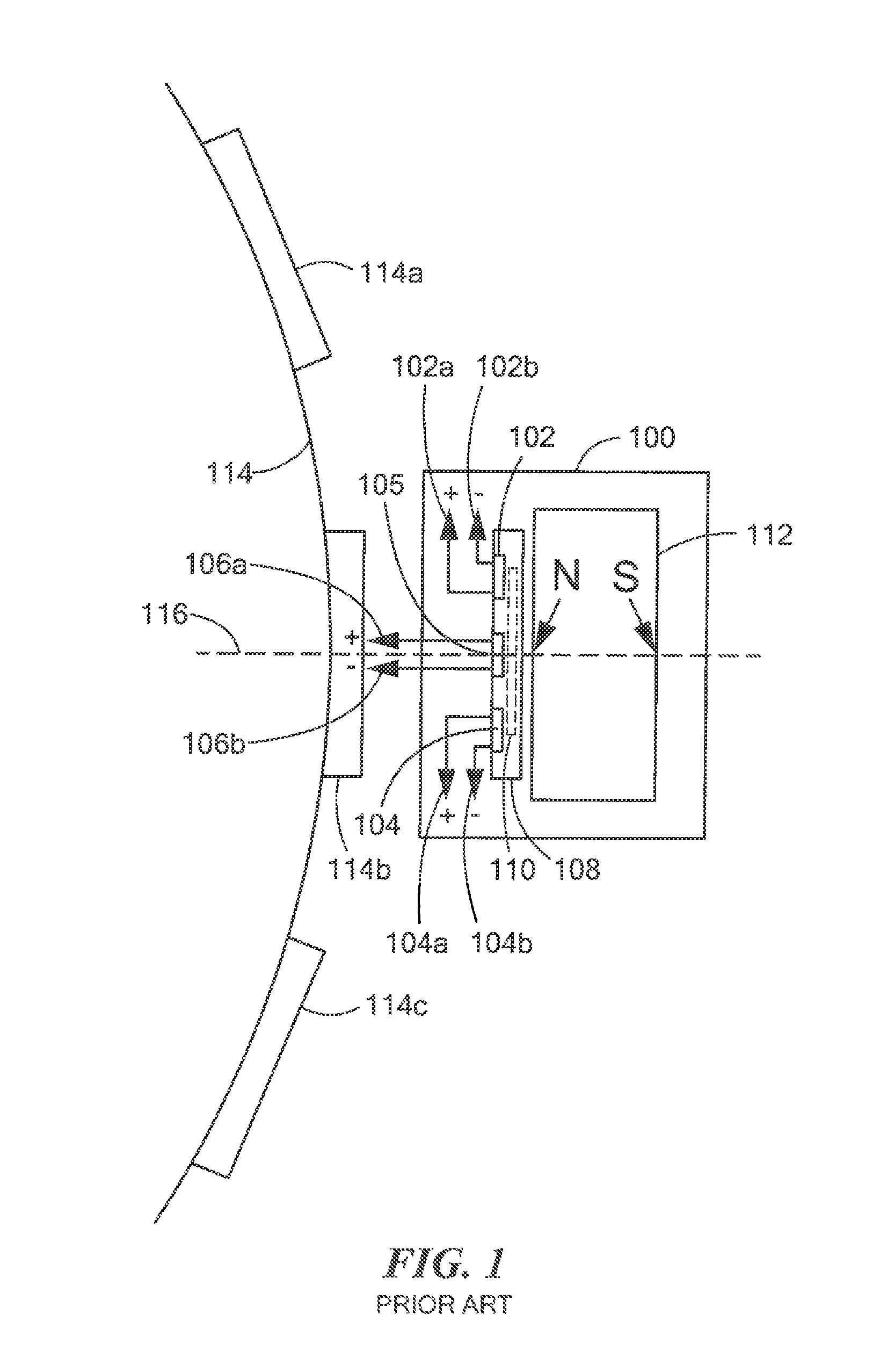
FIG. 1 is a block diagram showing a prior art magnetic field sensor proximate to a gear operable to rotate;
FIG. 2 is a block diagram showing a prior art electronic circuit that can be used in the prior art magnetic field sensor of FIG. 1;
FIG. 3 is a graph showing particular signals within the prior art electronic circuit of FIG. 2;
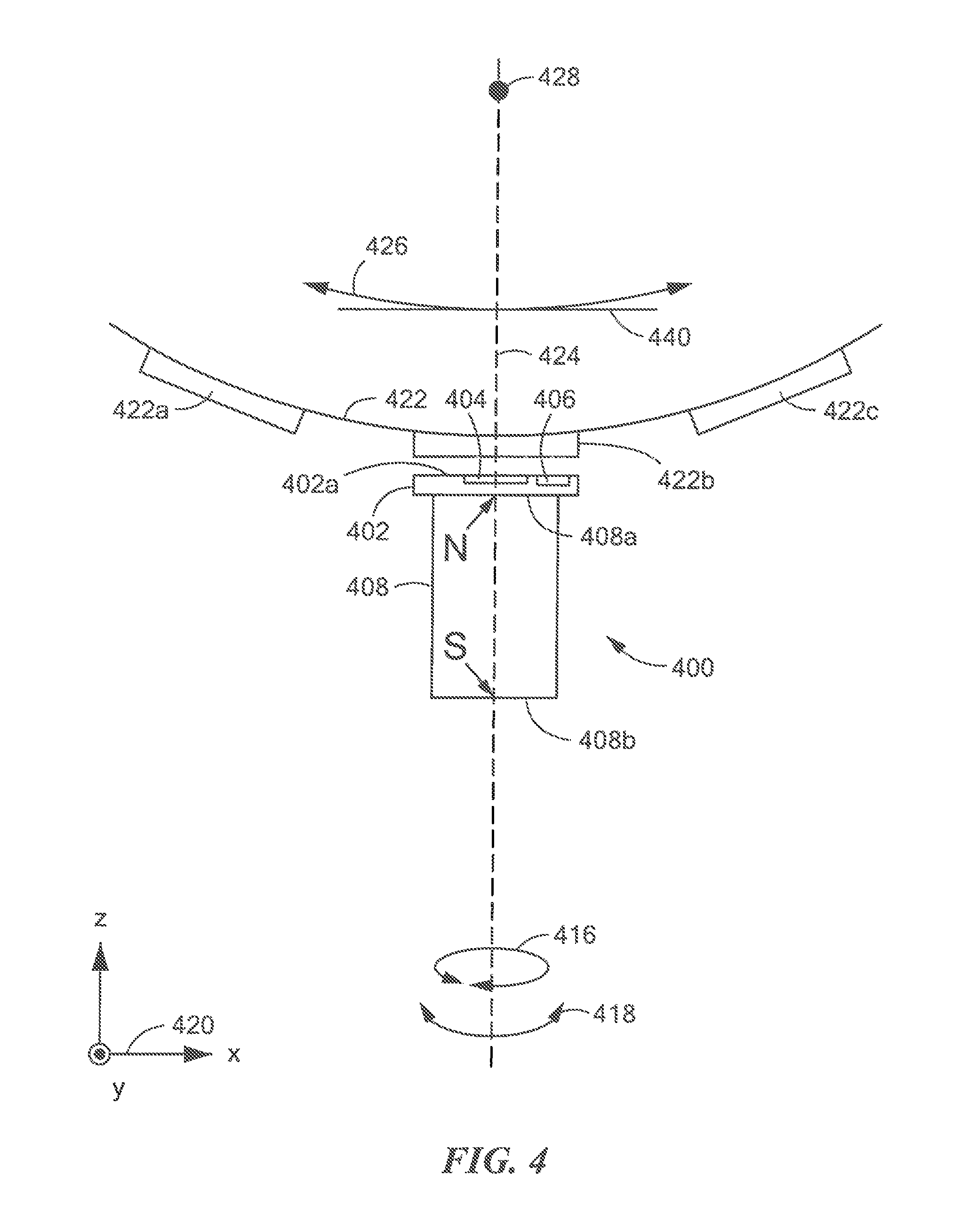
FIG. 4 is a block diagram showing a side view of another magnetic field sensor having a semiconductor substrate proximate to a gear operable to rotate;
FIG. 5 is a block diagram showing a top view of an illustrative substrate portion of a magnetic field sensor according to FIG. 4 and having two magnetic field sensing elements and an electronic circuit;
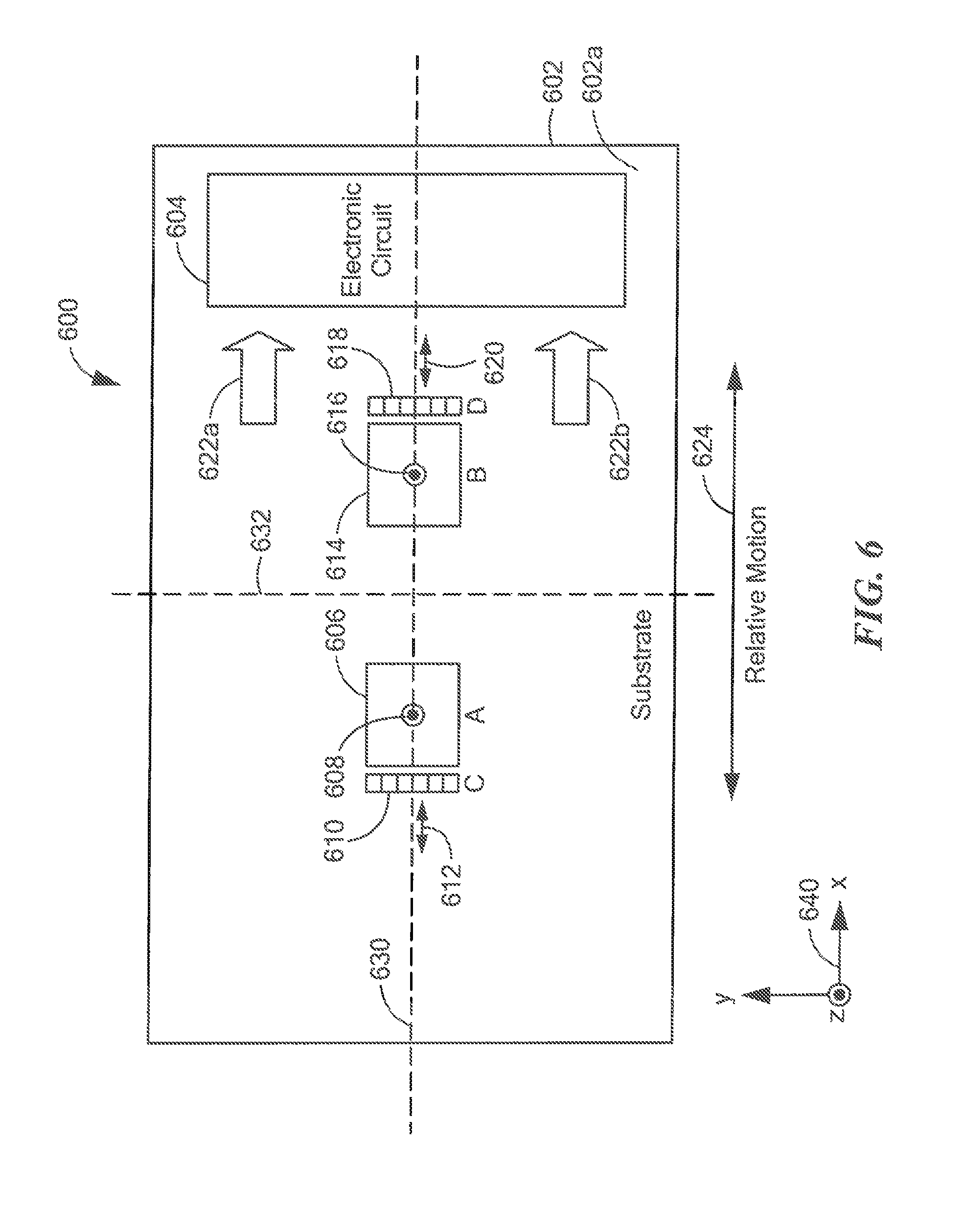
FIG. 6 is a block diagram showing a top view of an illustrative substrate portion of a magnetic field sensor according to FIG. 4 and having four magnetic field sensing elements and an electronic circuit;
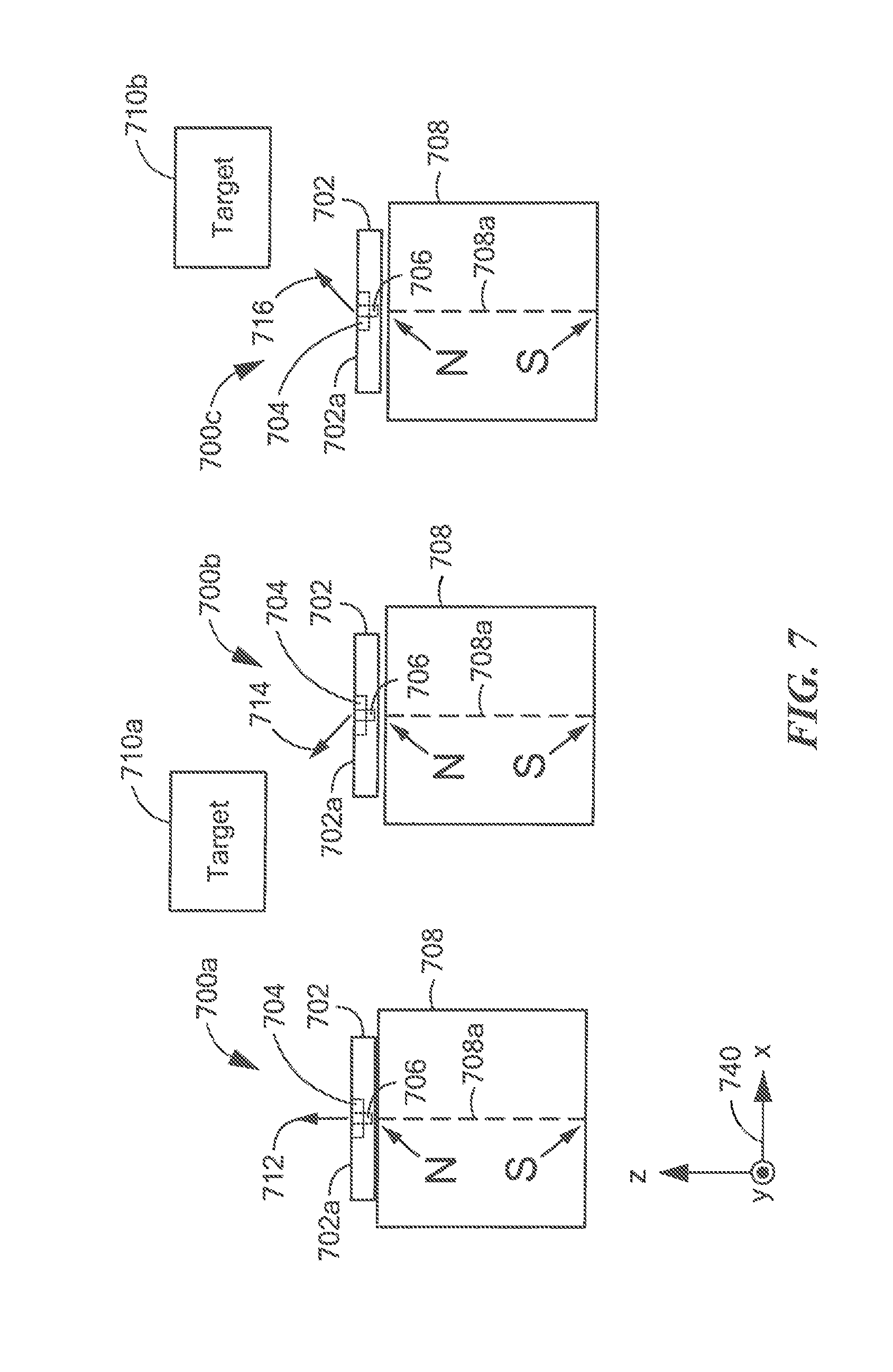
FIG. 7 is a block diagram showing a side view of a magnetic field sensor according to the substrate portion of the magnetic field sensor of FIG. 5 and showing an effect upon magnetic field lines as a ferromagnetic object passes;
FIG. 8 is a block diagram showing a side view of a magnetic field sensor according to the substrate portion of the magnetic field sensor of FIG. 6 and showing an effect upon magnetic field lines as a ferromagnetic object passes;
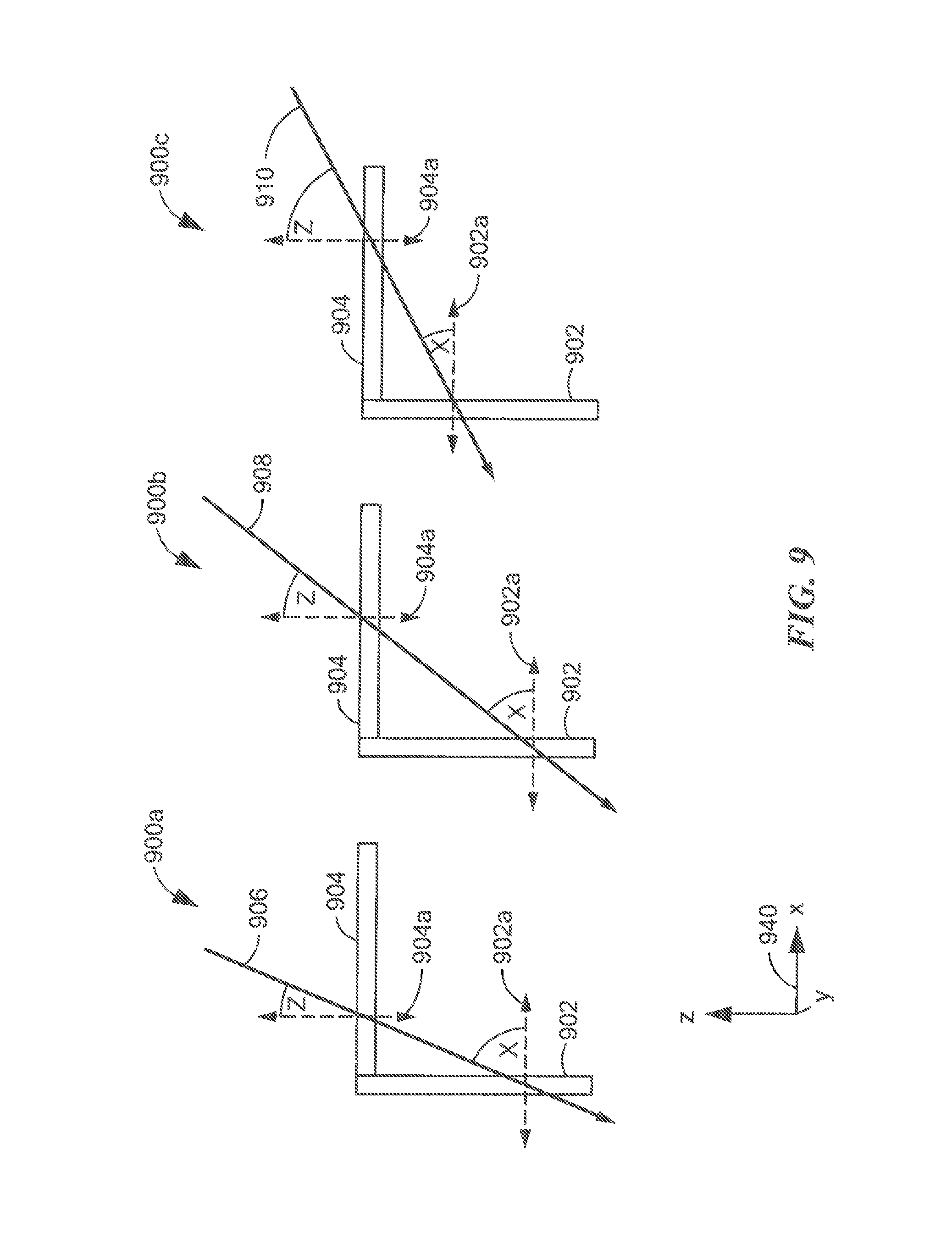
FIG. 9 is a block diagram showing magnetic field lines, planar Hall effect elements, and vertical Hall effect elements;
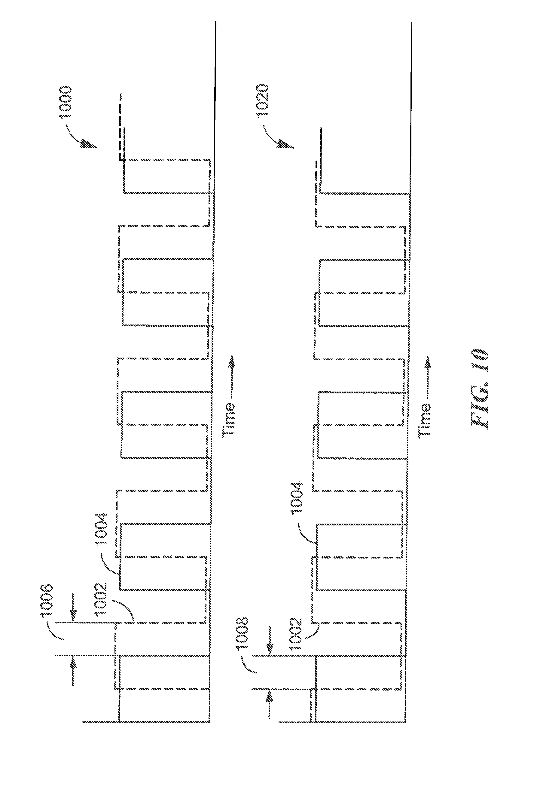
FIG. 10 is a graph showing particular signals within the electronic circuits of FIGS. 5 and 6;
FIG. 11 is a block diagram showing further details of an example of the electronic circuit of FIG. 5;
FIG. 12 is a block diagram showing further details of an example of the electronic circuit of FIG. 6;
FIG. 13 is a block diagram showing a top view of an illustrative substrate portion of a magnetic field sensor according to FIG. 4 and having six magnetic field sensing elements and an electronic circuit;
FIG. 14 is a block diagram showing further details of an example of the electronic circuit of FIG. 13;
FIG. 15 is a block diagram showing a top view of an illustrative substrate portion of a magnetic field sensor according to FIG. 4 and having four magnetic field sensing elements and an electronic circuit;
FIG. 16 is a block diagram showing further details of an example of the electronic circuit of FIG. 15; and
FIG. 17 is a block diagram showing two magnetoresistance elements coupled in a bridge arrangement that can be used in the magnetic field sensors and electronic circuits of FIGS. 4-9, and 11-16.
DETAILED DESCRIPTION
Before describing the present invention, some introductory concepts and terminology are explained.
As used herein, the term "magnetic field sensing element" is used to describe a variety of electronic elements that can sense a magnetic field. The magnetic field sensing element can be, but is not limited to, a Hall Effect element, a magnetoresistance element, or a magnetotransistor. As is known, there are different types of Hall Effect elements, for example, a planar Hall element, a vertical Hall element, and a Circular Vertical Hall (CVH) element. As is also known, there are different types of magnetoresistance elements, for example, a semiconductor magnetoresistance element such as Indium Antimonide (InSb), a giant magnetoresistance (GMR) element, an anisotropic magnetoresistance element (AMR), a tunneling magnetoresistance (TMR) element, and a magnetic tunnel junction (MTJ). The magnetic field sensing element may be a single element or, alternatively, may include two or more magnetic field sensing elements arranged in various configurations, e.g., a half bridge or full (Wheatstone) bridge. Depending on the device type and other application requirements, the magnetic field sensing element may be a device made of a type IV semiconductor material such as Silicon (Si) or Germanium (Ge), or a compound semiconductor material like Gallium-Arsenide (GaAs) or an Indium compound, e.g., Indium-Antimonide (InSb), or InGaA.
As is known, some of the above-described magnetic field sensing elements tend to have an axis of maximum sensitivity substantially parallel to a substrate that supports the magnetic field sensing element, and others of the above-described magnetic field sensing elements tend to have an axis of maximum sensitivity substantially perpendicular to a substrate that supports the magnetic field sensing element. In particular, planar Hall elements tend to have axes of sensitivity substantially perpendicular to a substrate, while metal based or metallic magnetoresistance elements (e.g., GMR, TMR, AMR) and vertical Hall elements tend to have axes of sensitivity parallel to a substrate.
As used herein, the term "magnetic field sensor" is used to describe a circuit that uses a magnetic field sensing element, generally in combination with other circuits. Magnetic field sensors are used in a variety of applications, including, but not limited to, an angle sensor that senses an angle of a direction of a magnetic field, a current sensor that senses a magnetic field generated by a current carried by a current-carrying conductor, a magnetic switch that senses the proximity of a ferromagnetic object, a rotation detector that senses passing ferromagnetic articles, for example, magnetic domains of a ring magnet, and a magnetic field sensor that senses a magnetic field density of a magnetic field.
The terms "parallel" and "perpendicular" are used in various contexts herein. It should be understood that the terms parallel and perpendicular do not require exact perpendicularity or exact parallelism, but instead it is intended that normal manufacturing tolerances apply, which tolerances depend upon the context in which the terms are used. In some instances, the term "substantially" is used to modify the terms "parallel" or "perpendicular." In general, use of the term "substantially" reflects angles that are beyond manufacturing tolerances, for example, within +/-ten degrees.
Examples below describe a particular gear as may be used upon an engine camshaft target object. However, similar circuits and techniques can be used with other cams or gears disposed upon the engine camshaft, or upon other rotating parts of an engine (e.g., crank shaft, transmission gear, anti-lock braking system (ABS)), or upon rotating parts of a device that is not an engine. Other applications may include linear translation sensors or other sensors where the target is not a rotating gear. The gear (or target) is not a part of the magnetic field sensors described below. The gear can have ferromagnetic gear teeth, which can be soft ferromagnetic objects, but which can also be hard ferromagnetic objects, patterns, or domains which may or may not have actual physical changes in their shape.
Also, while examples are shown below of magnetic field sensors that can sense ferromagnetic gear teeth or gear teeth edges upon a gear configured to rotate, the magnetic field sensors can be used in other applications. The other applications include, but are not limited to, sensing ferromagnetic objects upon a structure configured to move linearly.
As used herein, the term "baseline" and the phrase "baseline level" are used to describe a lowest magnitude (which may be near zero or may be some other magnetic field) of a magnetic field experienced by a magnetic field sensing element within a magnetic field sensor when the magnetic field sensor is operating in a system. In some systems, this lowest magnetic field occurs when a magnetic field sensor is proximate to a gear valley as opposed to a gear tooth.
It will be understood that, in general, a difference between the baseline level and a higher level achieved, for example, when a gear tooth is proximate to a magnetic field sensor, is related to an ability of the magnetic field sensor to differentiate between a gear tooth and a valley, and thus, related to accuracy of the magnetic field sensor.
While it is described above that a baseline level is generated when a magnetic field sensor is proximate to a gear valley and a higher level is achieved when the magnetic field sensor is proximate to a gear tooth, other physical arrangements are also possible, for example, a reverse arrangement for which a baseline level is generated when a magnetic field sensor is proximate to a gear tooth and a higher level is achieved when the magnetic field sensor is proximate to a gear valley.
As used herein, the term "processor" is used to describe an electronic circuit that performs a function, an operation, or a sequence of operations. The function, operation, or sequence of operations can be hard coded into the electronic circuit or soft coded by way of instructions held in a memory device. A "processor" can perform the function, operation, or sequence of operations using digital values or using analog signals.
In some embodiments, the "processor" can be embodied in an application specific integrated circuit (ASIC), which can be an analog ASIC or a digital ASIC. In some embodiments, the "processor" can be embodied in a microprocessor with associated program memory. In some embodiments, the "processor" can be embodied in a discrete electronic circuit, which can be an analog or digital.
As used herein, the term "module" is used to describe a "processor."
A processor can contain internal processors or internal modules that perform portions of the function, operation, or sequence of operations of the processor. Similarly, a module can contain internal processors or internal modules that perform portions of the function, operation, or sequence of operations of the module.
While electronic circuits shown in figures herein may be shown in the form of analog blocks or digital blocks, it will be understood that the analog blocks can be replaced by digital blocks that perform the same or similar functions and the digital blocks can be replaced by analog blocks that perform the same or similar functions. Analog-to-digital or digital-to-analog conversions may not be explicitly shown in the figures, but should be understood.
As used herein, the term "predetermined," when referring to a value or signal, is used to refer to a value or signal that is set, or fixed, in the factory at the time of manufacture, or by external means, e.g., programming, thereafter. As used herein, the term "determined," when referring to a value or signal, is used to refer to a value or signal that is identified by a circuit during operation, after manufacture.
As used herein, the term "active electronic component" is used to describe an electronic component that has at least one p-n junction. A transistor, a diode, and a logic gate are examples of active electronic components. In contrast, as used herein, the term "passive electronic component" as used to describe an electronic component that does not have at least one p-n junction. A capacitor and a resistor are examples of passive electronic components.
Referring now to FIG. 1, an example conventional magnetic field sensor 100 is responsive to a gear 114 having gear teeth, e.g., gear teeth 114a, 114b, 114c. The magnetic field sensor 100 includes three magnetic field sensing elements 102, 104, 106 coupled to an electronic circuit 110 upon a substrate 108. In some embodiments, the magnetic field sensing elements 102, 104 are separated in a direction substantially perpendicular to an axis 116 by a distance between about 1.5 millimeters and about 3.0 millimeters, and the magnetic field sensing element 106 is located midway between the magnetic field sensing elements 102, 104.
The three magnetic field sensing elements 102, 104, 106 and an electronic circuit 110 can be disposed upon (i.e., integrated within or upon) a substrate 108. Here, the magnetic field sensing elements 102, 104, 106 are shown to be planar Hall effect elements. The magnetic field sensor 100 can also include a magnet 112, resulting in a back-biased arrangement. The magnet 112 is configured to generate a magnetic field, which is generally directed along the axis 116 at the position of the magnetic field sensing elements 102, 104, 106.
The electronic circuit 110 is configured to generate an output signal (not shown). An exemplary electronic circuit 110 is described below in conjunction with FIG. 2. Let it suffice here to say that the electronic circuit 110 generates a difference of signals. Thus, the magnetic field sensor 100 is an edge detector and not a tooth detector.
An "edge detector" is not able to identify whether the magnetic field sensor 100 is proximate to a gear tooth or a gear valley. However, the edge detector is able to sense edges of gear teeth as they move past the magnetic field sensor 350. In contrast, a "tooth detector" is able to identify whether a magnetic field sensor is proximate to a gear tooth or valley.
The output signal, when the gear 114 is rotating, is indicative speed of rotation of the gear 114 and can also be indicative of a direction of rotation of the gear 114 by circuits and techniques described more fully below.
In some embodiments, the magnet 112 can have a central core (not shown). The central core (not shown) can be comprised of a soft ferromagnetic material disposed within the magnet 112. An example of a magnet with a core is described in U.S. Pat. No. 6,278,269, entitled "Magnet Structure," issued Aug. 21, 2001, which patent is assigned to the assignee of the present invention and incorporated herein by reference in its entirety. As described in U.S. Pat. No. 6,278,269, the pole configuration provided by the magnet with the core lowers the base field (or baseline) of a flux density of the magnetic field at some points above the surface of the core (e.g., to the left of the magnet 112 as shown) when a valley of the gear 114 is proximate to the magnetic field sensor 100. A predetermined baseline (e.g., within a range of about +/six hundred Gauss) at the magnetic field sensing elements 102, 104, 106, can be achieved with proper design.
The above-described low baseline, which occurs when the magnetic field sensor is proximate to a gear valley, results in the electronic circuit 110 being able to identify gear teeth as they pass by the magnetic field sensor 100.
As described above, the central core can result in a low baseline when the magnetic field sensing element 102, 104, 106 are proximate to a valley in the gear 114. However, the magnetic field sensor 100 uses three magnetic field sensing elements, generating a respective three differential output signals 102a, 102b, and 104a, 104b, and 106a, 106b. As will be described in conjunction with FIG. 2, pairs of signals representative of the three differential output signals 102a, 102b, and 104a, 104b, and 106a, 106b are subtracted in the electronic circuit 110. Thus, when the three magnetic field sensing elements 102, 104, 106 are proximate to a valley in the gear 114, the differential nature of the combined signal can result in an even lower combined signal than can achieved by the low baseline alone. Also, when the three magnetic field sensing elements 102, 104, 106 are proximate to a gear tooth, the low combined signal is also achieved. Only when some of the magnetic field sensing elements 102, 104, 106 are proximate to a gear tooth and others are proximate to a gear valley, i.e., proximate to a gear edge, is the combined signal increased. Thus, the magnetic field sensor 100 is an edge detector, and not a tooth detector.
The differencing of pairs of the three differential signals 102a, 102b, and 104a, 104b, and 106a, 106b results in an improved accuracy of the magnetic field sensor 100. For example, the magnetic field sensor 100 is less influenced by external magnetic fields, i.e., noise magnetic fields and/or by nose electromagnetic field, i.e., by noise electrical signals, that the three magnetic field sensing elements 102, 104, 106 may experience in the same way.
Referring now to FIG. 2, a conventional electronic circuit 140 can include amplifiers 148, 150, 152 coupled to receive differential signals 142a, 142b, and 144a, 144b, and 146a, 146b, respectively. The differential signal 142a, 142b can be the same as or similar to the differential signal 102a, 102b, the differential signal 144a, 144b can be the same as or similar to the differential signals 104a, 104b, and the differential signal 146a, 146b can be the same as or similar to the differential signal 106a, 106b generated, respectively, by the magnetic field sensing elements 102, 104, 106 of FIG. 1. The amplifiers 148, 150, 152 are configured to generate amplified signals 148a, 150a, 152a, respectively.
The amplified signals 148a, 152a are received by a first differencing module 154, which is configured to generate a first difference signal 154a. The amplified signals 150a, 152a are received by a second differencing module 156, which is configured to generate a second difference signal 156a.
The electronic circuit 140 can include a first automatic gain control/automatic offset control (AGC/AOA) module 160 coupled to receive the first difference signal 154a. The electronic circuit 140 can include a second automatic gain control/automatic offset control (AGC/AOA) module 166 coupled to receive the second difference signal 156a.
The first AGC/AOA module 160 is operable to generate a first calibrated signal 160a and the second AGC/AOA module 166 is operable to generate a second calibrated signal 166a. The calibrated signals 160a 166a can have signal values adjusted in gain so that AC signal components thereof can match in amplitude, and signal values for which DC offset signal components thereof are substantially removed.
A first rotation detector module 162a is coupled to receive the first calibrated signal 160a and a second rotation detector 168 is coupled to receive the second calibrated signal 166a.
Generally speaking, the rotation detector modules 162, 166 are operable to convert the calibrated signals 160a, 166a from multi-state signals, e.g., analog sinusoid signals, to two-state signals 162a, 168a, respectively. This conversion can be accomplished, for example, by comparing the first calibrated signal 160a with one or more threshold values to generate the first two-state signal 162a and comparing the second calibrated signal 166a with another one or more threshold values to generate the second two-state signal 168a.
A variety of ways have been used to generate the above-described threshold values. For example, in one type of magnetic field sensor described in U.S. Pat. No. 6,525,531, issued Feb. 25, 2003, a positive digital-to-analog converter (PDAC) and a negative digital-to-analog converter (NDAC) track positive and negative peaks of magnetic field signal, respectively, for use in generating a threshold signal. A varying magnetic field signal is compared to the threshold signal to generate a two-state signal. Other ways to generate the above-described threshold values are described, for example, in U.S. Pat. No. 7,368,904, issued May 6, 2008, and U.S. Pat. No. 7,253,614, issued Aug. 7, 2007, and U.S. Pat. No. 7,772,838, issued Aug. 10, 2010, all of which are assigned to the assignee of the present invention and both of which are incorporated by reference herein in their entirety.
The two-state signals 162a, 168a each have state transitions, rates of which are indicative of a speed of rotation of the gear 114. The two-state signals 162a, 168a also have a relative phase, one having state transitions that occur before the other or vice versa. A sign (plus or minus) of a relative phase of the two-state signals 162a, 168a is indicative of a direction of rotation of the gear 114.
The sign of the relative phase is most easily determined and least subject to errors caused for example, by magnetic and electrical noise, if the relative phase between the two-state signals 162a, 168a is large. Phase separation between the two state signals 162a, 168a is ultimately determined according to a separation between the magnetic field sensing elements 102, 104 and a speed of rotation of the gear 114. In order to keep the substrate 108 small, it is desirable that the separation between the magnetic field sensing elements 102, 104 is small.
As described above, in some embodiments, the magnetic field sensing elements 102, 104 are separated in a direction substantially perpendicular to the axis 116 by a distance between about 1.5 millimeters and about 3.0 millimeters, and the magnetic field sensing element 106 is located midway between the magnetic field sensing elements 102, 104.
For typical gears, e.g., the gear 104, it can be determined that the relative phase between the two-state signals 162a, 168a tends to be small, for example, in the range of +/-ten to fifteen degrees.
A speed/direction module 164 is coupled to receive the two-state signals 162a, 168a and configured to generate a speed/direction signal 164a representative of at least one of the speed of rotation or the direction of rotation of the gear.
Referring now to FIG. 3, first and second graphs 300, 320 have horizontal axes with scales in units of time in arbitrary units and vertical axes with scales in units of amplitude in arbitrary units.
In the first graph 300, a first signal 302 is indicative of the first two-state signal 162a of FIG. 2 when the gear 114 is rotating in a first direction, and a second signal 304 is indicative of the second two-state signal 168a of FIG. 2 when the gear 114 is rotating in the first direction. Each edge (state transition) of the signals 302, 304 can be indicative of a gear tooth edge passing by the magnetic field sensor 100.
A phase difference 306 indicates a phase difference when the first and second two-state signals are operating in response to the gear 114 rotating in the first direction.
In the second graph 320, the same first signal 302 is indicative of the first two-state signal 162a of FIG. 2 when the gear 114 is rotating in a second different direction, and the same second signal 304 is indicative of the second two-state signal 168a of FIG. 2 when the gear 114 is rotating in the second direction. Again, each edge (state transition) of the signals 302, 304 can be indicative of a gear tooth edge passing by the magnetic field sensor 100.
A phase difference 308 indicates a phase difference when the first and second two-state signals are operating in response to the gear 114 rotating in the second direction.
It should be apparent that the phase differences 306, 308 have opposite signs. The signs are indicative of the direction of rotation of the gear 114.
In addition, from discussion above in conjunction with FIG. 2, it should be apparent that the phase differences 306, 308 are fairly small and subject to various noises that can result in a detection of the wrong sign of the phase and a corresponding indication of the wrong direction of rotation of the gear 114, either intermittently or statically.
Referring now to FIG. 4, an illustrative magnetic field sensor 400 includes a substrate 402 having a first surface 402a, a magnetic field sensing element region 404 having magnetic field sensing elements therein and disposed in or upon the first surface 402a, and an electronic circuit 406 coupled to the magnetic field sensing element region 404 and disposed in or upon the first surface 402a. In some embodiments, the substrate 402 is a semiconductor substrate 402.
Here it is shown that the first surface 402a can be positioned proximate to a ferromagnetic gear 422 having gear teeth 422a, 422b, 422c, and others. However, in other embodiments, the first surface 402a upon which magnetic field sensing elements are disposed in or upon can be positioned in the other direction, distal from the gear 422.
While a rotating gear 422 having ferromagnetic gear teeth, e.g., 422a, is described in examples herein, in other embodiments, an object having ferromagnetic features that move linearly or in some other motion can be used and speed of movement and direction of the movement can be detected with circuits and techniques herein.
The substrate 402 can be disposed substantially parallel to an x-y plane of axes 420.
A magnet 408 can be disposed proximate to the substrate 402 such that a so-called "magnet axis" 424 passes through a north pole 408a, N, and a south pole 408b, S in a direction substantially perpendicular to the surface 402a of the substrate 402. In some embodiments, the axis 424 can also pass though an axis of rotation 428 of the gear. The magnet axis 424 can insect the surfaces 408a, 408b central to the surfaces 408a, 408b.
The magnetic field sensor 400 can rotate in a direction 416 through about +/-thirty degrees while maintaining some accuracy. The magnetic field sensor 400 can also rotate in a direction 418 though about +/-thirty degrees while maintaining some accuracy.
The gear 422 can rotate in a direction 426. A tangent line 440 can be tangent to the rotation direction 426.
Now referring to FIG. 5, a substrate portion of a magnetic field sensor 500 can include a substrate 502 the same as or similar to the substrate 402 of FIG. 4. The substrate 502 can be disposed parallel to the same x-y plane of coordinate axes 540 as indicated by the coordinate axes 420 of FIG. 4
A surface 502a of the substrate 502 can be the same as or similar to the surface 402a of the substrate 402 of FIG. 4.
An electronic circuit 516 can be disposed in or upon the surface 502a of the substrate 502. The electronic circuit 516 can be the same as or similar to the electronic circuit 406 of FIG. 4.
A first magnetic field sensing element 504 and a second magnetic field sensing element 508 can be the same as or similar to magnetic field sensing elements in the magnetic field sensing element region 404 of FIG. 4
A ferromagnetic object can move with a direction substantially parallel to a line 514, which can be, for example, representative of a line substantially parallel to the tangent line 440 of FIG. 4. The ferromagnetic object can move directly over the substrate point at which the orthogonal axes 530, 532 intersect.
The first magnetic field sensing element 504 can be a planar Hall effect element 504 (also sometimes referred to as a horizontal Hall effect element). As described above, the planar Hall effect element 504 has an axis of maximum sensitivity 506 substantially parallel to a z-axis of coordinate axes 540. The axis of maximum sensitivity 506 is substantially perpendicular to the surface 502a of the substrate.
In contrast, the second magnetic field sensing element 508 can be a vertical Hall effect element 508. As described above, the vertical Hall effect element 508 has an axis of maximum sensitivity 510 substantially parallel to the x-axis of the coordinate axes 540, i.e., substantially parallel to the surface 502a of the substrate. The maximum response axis 506 can be substantially perpendicular to the maximum response axis 510.
Electronic signals 512, described more fully below, couple the first and second magnetic field sensing elements 504, 508 to the electronic circuit 516.
A magnet (not shown) can be disposed under the substrate 502 and can have the same orientation and characteristics described below in conjunction with the magnet 408 of FIG. 4.
First and second orthogonal axes 530, 532, respectively, substantially parallel to the first surface 502a of the substrate 502, are indicative of examples of relative placements of the first and second magnetic field sensing elements 504, 508, and also indicative of an example of a relative position of the magnet 408 of FIG. 4. The axis 424 of the magnet can intersect in a z direction (see coordinate axes 540) at an intersection of the first and second orthogonal axes 530, 532, the intersection also referred to herein as a "substrate point." The first and second magnetic field sensing elements 504, 508 can be disposed along the first or second orthogonal axes 530, 532.
A center of the first magnetic field sensing element 504 can be disposed along the first orthogonal axis 530. In some embodiments, the center of the first magnetic field sensing element 504 can be disposed at the intersection of the first and second coordinate axes 530, 532.
A center of second magnetic field sensing element 508b can be disposed along the first or second orthogonal axis 530, 540, here shown to be along the second orthogonal axis 532. However, other placements of the second magnetic field sensing element 508 are also possible.
Referring now to FIG. 6, a substrate portion of a magnetic field sensor 600 can include a substrate 602 the same as or similar to the substrate 402 of FIG. 4. The substrate 602 can be disposed parallel to the same x-y plane of coordinate axes 640 as indicated by the coordinate axes 420 of FIG. 4
A surface 602a of the substrate 602 can be the same as or similar to the surface 402a of the substrate 402 of FIG. 4.
An electronic circuit 604 can be disposed in or upon the surface 602a of the substrate 602. The electronic circuit 604 can be the same as or similar to the electronic circuit 406 of FIG. 4.
A first magnetic field sensing element 606, a second magnetic field sensing element 610, a third magnetic field sensing element 614, and a fourth magnetic field sensing element 618 can be the same as or similar to magnetic field sensing elements in the magnetic field sensing element region 404 of FIG. 4
A ferromagnetic object (not shown) can move with a direction substantially parallel to a line 624, which can be, for example, representative of a line substantially parallel to the tangent line 440 of FIG. 4. The ferromagnetic object can move directly over the substrate point at which the orthogonal axes 630, 632 intersect.
The first magnetic field sensing element 606 and the third magnetic field sensing element 614 can be planar Hall effect elements 606, 614 (also sometimes referred to as horizontal Hall effect elements). As described above, the planar Hall effect element 606 and has an axis of maximum sensitivity 608 and the planar Hall effect element 614 has an axis of maximum sensitivity 616, both substantially parallel to a z-axis of coordinate axes 540. The axes of maximum sensitivity 608, 616 are substantially perpendicular to the surface 602a of the substrate 602.
In contrast, the second magnetic field sensing element 610 and the fourth magnetic field sensing element 618 can be vertical Hall effect elements 610, 618. As described above, the vertical Hall effect elements 610, 618 have respective axes of maximum sensitivity 612, 620 substantially parallel to the x-axis of the coordinate axes 640, i.e., substantially parallel to the surface 602a of the substrate. The maximum response axes 608, 616 can be substantially perpendicular to the response axes 612, 620.
Electronic signals 622a, 622b, described more fully below, couple the first, second, third and fourth magnetic field sensing elements 606, 610, 614, 618, respectively, to the electronic circuit 604
A magnet (not shown) can be disposed under the substrate 602 and can have the same orientation and characteristics described below in conjunction with the magnet 408 of FIG. 4.
First and second orthogonal axes 630, 632, respectively, substantially parallel to the first surface 602a of the substrate 602, are indicative of examples of relative placements of the first, second, third and fourth magnetic field sensing elements 606, 610, 614, 618, respectively, and also indicative of an example of a relative position of the magnet 408 of FIG. 4. The axis 424 of the magnet can intersect in a z direction (see coordinate axes 640) at an intersection of the first and second orthogonal axes 630, 632, the intersection also referred to herein as a "substrate point." The first, second, third, and fourth magnetic field sensing elements 608, 610, 614, 618, respectively, can be disposed along the first or second orthogonal axes 630, 632 and can also be disposed apart from the substrate point.
Centers of the first and third magnetic field sensing elements 606, 614, respectively, can be disposed along the first orthogonal axis 630. In some embodiments, a midpoint between centers of the first and third magnetic field sensing elements 606, 614, respectively, can be disposed at the intersection of the first and second coordinate axes 630, 632.
Centers of second and fourth magnetic field sensing elements 610, 618, respectively, can be disposed along the first or second orthogonal axis 630, 632, here shown to be along the first orthogonal axis 630. In some embodiments, a midpoint between centers of the second and fourth magnetic field sensing elements 610, 618, respectively, can be disposed at the intersection of the first and second coordinate axes 630, 632. However, other placements of the second and fourth magnetic field sensing elements 610, 618 are also possible.
Referring now to FIG. 7, shown in three views 700a, 700b, 700c, a magnetic field sensor 700 has a substrate 702 that is the same as or similar to the substrate 502 of FIG. 5. A planar Hall effect element 704 is the same as or similar to the planar Hall effect element 506 of FIG. 5. A vertical Hall effect element 706 is the same as or similar to the vertical Hall effect element 508 of FIG. 5. A magnet 708 is the same as or similar to the magnet 408 of FIG. 4. An axis 708a is the same as or similar to the magnet axis 424 of FIG. 4, passing between north and south poles of the magnet 708.
A ferromagnetic target 710 (here shown at two positions 710a, 710b) is shown at two positions relative to the views 700b, 700c of the magnetic field sensor 700. In the left view 700a, a ferromagnetic target is far away and not shown. In the center view 700b, a ferromagnetic target 710a is to the left of the view 700b of the magnetic field sensor 700. In the right view 700c, the ferromagnetic target 710b is to the right of the view 700c of the magnetic field sensor 700.
A line of magnetic flux 712 (among many such lines) is substantially parallel to the axis 708a of the magnet 708 in the view 700a when no ferromagnetic object is nearby.
A line of magnetic flux 714 has a head angled to the left as shown in the view 700b when the ferromagnetic target 710a is to the left in the view 700b of the magnetic field sensor 700.
A line of magnetic flux 716 has a head angled to the right as shown in the view 700c when the ferromagnetic target 710b is to the right in the view 700c of the magnetic field sensor 700.
Thus, it can be seen that the magnetic flux changes angle when the ferromagnetic target 710a, 710b passes by the magnetic field sensor 700a, 700b, 700c in a direction substantially parallel to an x-axis of the coordinate axes 740.
It should be apparent that an output signal from the planar Hall effect element 704 has an amplitude responsive to a projection of a sensed magnetic field upon its maximum response axis, i.e., to a projection upon an axis centered with the planar Hall effect element 704 and substantially parallel to the z-axis (i.e., substantially perpendicular to the surface 702a of the substrate 702). It should also be apparent that an output signal from the vertical Hall effect element 704 has an amplitude responsive to a projection of a sensed magnetic field upon its maximum response axis, i.e., to a projection upon an axis centered with the vertical hall effect element 706 and substantially parallel to the x-axis (i.e., substantially parallel to the surface 702a of the substrate 702). Thus, both the planar Hall effect element 704 and the vertical Hall effect element 706 have respective varying output signals as the ferromagnetic target object 710a, 710b passes by in a direction of the x-axis of the coordinate axes 740. Further explanation of operation of the magnetic field sensor 700a, 700b, 700c is given below.
The ferromagnetic target object 710a, 710b can be representative of a gear tooth on a gear, for example, one of the gear teeth, e.g., 422b, on the gear 422 of FIG. 4. However, the ferromagnetic target object 710a, 710b can be representative of any other ferromagnetic target object.
Referring now to FIG. 8, shown in three views 800a, 800b, 800c, a magnetic field sensor 800 has a substrate 802 that is the same as or similar to the substrate 502 of FIG. 5. A first magnetic field sensing element 804 comprising a planar Hall effect element 804 is the same as or similar to the first magnetic field sensing element 606 of FIG. 6, i.e., the planar Hall effect element 606 of FIG. 6.
A second magnetic field sensing element 806 comprising a vertical Hall effect element 806 is the same as or similar to the second magnetic field sensing element 610 of FIG. 6, i.e., the vertical Hall effect element 610 of FIG. 6.
A third magnetic field sensing element 808 comprising a planar Hall effect element 808 is the same as or similar to the third magnetic field sensing element 614 of FIG. 6, i.e., the planar Hall effect element 614 of FIG. 6.
A fourth magnetic field sensing element 810 comprising a vertical Hall effect element 810 is the same as or similar to the fourth magnetic field sensing element 618 of FIG. 6, i.e., the vertical Hall effect element 618 of FIG. 6.
A magnet 808 is the same as or similar to the magnet 408 of FIG. 4. An axis 812a is the same as or similar to the magnet axis 424 of FIG. 4, passing between north and south poles of the magnet 808.
A ferromagnetic target 826 (here shown at two positions 826a, 826b) is shown at two positions relative to the views 800b, 800c of the magnetic field sensor 800. In the left view 800a, a ferromagnetic target is far away and not shown. In the center view 800b, a ferromagnetic target 826a is to the left of the view 800b of the magnetic field sensor 800. In the right view 800c, the ferromagnetic target 826b is to the right of the view 800c of the magnetic field sensor 800.
Lines of magnetic flux 814, 816 (among many such lines) have heads symmetrically to the left and to the right, respectively, relative to the axis 812a of the magnet 812 in the view 800a when no ferromagnetic object is nearby.
Lines of magnetic flux 818, 820 have heads in the view 800b such that the line of flux 818 is less angled to the left than the line of magnetic flux 814, when the ferromagnetic target 826a is to the left in the view 800b of the magnetic field sensor 800.
Lines of magnetic flux 822, 824 have heads in the view 800c such that the line of flux 824 is less angled to the right than the line of magnetic flux 816, when the ferromagnetic target 826b is to the right in the view 800c of the magnetic field sensor 800.
Thus, it can be seen that the magnetic flux changes angles when the ferromagnetic target 810a, 810b passes by the magnetic field sensor 800a, 800b, 800c in a direction substantially parallel to an x-axis of the coordinate axes 840.
It should be apparent that respective output signals from the planar Hall effect elements 804, 808 have respective amplitudes responsive to projections of respective sensed magnetic fields upon their respective maximum response axes, i.e., to projections upon axes centered with the planar Hall effect elements 804, 808 and substantially parallel to the z-axis (i.e., substantially perpendicular to the surface 802a of the substrate 802). It should also be apparent that respective output signals from the vertical Hall effect elements 806, 810 have respective amplitudes responsive to projections of respective sensed magnetic fields upon their respective maximum response axes, i.e., to projections upon axes centered with the vertical Hall effect elements 806, 810 and substantially parallel to the x-axis (i.e., substantially parallel to the surface 802a of the substrate 802). Thus, both the planar Hall effect elements 804, 808 and the vertical Hall effect elements 806, 810 have varying output signals as the ferromagnetic target object 826a, 826b passes by in a direction of the x-axis of the coordinate axes 840. Further explanation of operation of the magnetic field sensor 800a, 800b, 800c is given below.
The ferromagnetic target object 826a, 826b can be representative of a gear tooth on a gear, for example, one of the gear teeth, e.g., 422b, on the gear 422 of FIG. 4. However, the ferromagnetic target object 826a, 826b can be representative of any other ferromagnetic target object.
Referring now to FIG. 9, three views 900as, 900b, 900c show a representation of a vertical Hall effect element 902 with a maximum response axis 902a and a planar Hall effect element 904 with a maximum response axis 904a.
A line of magnetic flux 906 is at a first angle, a line of magnetic flux 908 is at a second angle, and a line of magnetic flux 910 is at a third angle. It should be apparent that the three lines of magnetic flux 906, 908, 910 are representative of lines of magnetic flux that pass through the vertical Hall effect element 902 (e.g., 706, 806, 810) and through the planar Hall effect element 904 (e.g., 704, 804, 808) as the ferromagnetic target objects of FIGS. 7 and 8 pass by respective magnetic field sensor.
The vertical Hall effect element 902 has an axis of maximum sensitivity 902a. The planar Hall effect element 904 has an axis of maximum sensitivity 904a.
The vertical Hall effect element 902 has an output signal proportional to a projection of the magnetic field (906, 908, 910) on the axis of maximum sensitivity 902a. The planar Hall effect element 904 has an output signal proportional to a projection of the magnetic field (906, 908, 910) on the axis of maximum sensitivity 904a. The projections are related to the angles X and Z, respectively, as shown.
It will be apparent that the output signal from the vertical Hall effect element 902 becomes greater in amplitude as the magnetic flux changes from magnetic flux 906 to 908 to 910. Conversely, it will be apparent that the output signal from the planar Hall effect element 904 becomes lesser as the magnetic flux changes from magnetic flux 906 to 908 to 910.
If the magnetic flux were to move back and forth in alternating directions as represented by the views 700a, 700b, 700c and 800a, 800b, 800c as a ferromagnetic object passes by, the output signals from the vertical Hall effect element and the planar Hall effect element would be sinusoids that, within extreme limits, are always ninety degrees apart, regardless of the frequency of the sinusoid, i.e., regardless of the speed of motion of the ferromagnetic object, e.g., regardless of the speed of rotation of the gear 422 of FIG. 4 with ferromagnetic teeth.
Referring now to FIG. 10, first and second graphs 1000, 1020 have horizontal axes with scales in units of time in arbitrary units and vertical axes with scales in units of amplitude in arbitrary units.
In the first graph 1000, a first signal 1002 is indicative of a first two-state signal described in conjunction with figures below when the gear 422 of FIG. 4 is rotating in a first direction, and a second signal 1004 is indicative of a second two-state signal described in conjunction with figures below when the gear 422 is rotating in the first direction. Each edge (state transition) of the signals 1002, 1004 can be indicative of a gear tooth edge passing by the magnetic field sensor 400 of FIG. 4
A phase difference 1006 indicates a phase difference when the first and second two-state signals are operating in response to the gear 422 rotating in the first direction.
In the second graph 1020, the same first signal 1002 is indicative of the first two-state signal described in conjunction with figures below when the gear 422 is rotating in a second different direction, and the same second signal 1004 is indicative of the second two-state signal described in conjunction with figures below when the gear 422 is rotating in the second direction. Again, each edge (state transition) of the signals 1002, 1004 can be indicative of a gear tooth edge passing by the magnetic field sensor 100.
A phase difference 1008 indicates a phase difference when the first and second two-state signals 1002, 1004 are operating in response to the gear 422 rotating in the second direction.
It should be apparent that the phase differences 1006, 1008 have opposite signs. The signs are is indicative of the direction of rotation of the gear 422.
The phase differences are the result of magnetic field sensor signals described above in FIG. 10 to be ninety degrees apart. Comparing the ninety degree phase differences to the smaller phase difference of FIG. 3, direction detection is much less subject to various noises that can otherwise result in a detection of the wrong sign of the phase and a corresponding indication of the wrong direction of rotation of the gear 422.
The phase separations 1006, 1008 can remain the same for all rotation speed of the gear 422 of FIG. 4
Referring now to FIG. 11, an electronic circuit 1100 can be the same as the electronic circuit 406 of FIG. 4 when the magnetic field sensor 400 of FIG. 4 includes the substrate portion 500 of FIG. 5, having two magnetic field sensing element 504, 508. The first magnetic field sensing element 504 of FIG. 5 provides a differential signal 1102 and the second magnetic field sensing element 508 provides a differential signal 1112 to amplifiers 1104, 1114, respectively.
In accordance with the discussion above in conjunction with FIGS. 9 and 10, the differential signals 1102, 1112 have a ninety degree phase relationship when the gear 422 of FIG. 4 rotates, for all rotational speeds of the gear 422.
Amplifiers 1104, 1114, are coupled to receive the differential signals 1102, 1112, respectively, and operable to generate amplified signals 1104a, 1114a, which are received by AGC/AOA modules 1106, 1116, respectively.
The AGC/AOA modules 1106 1116, rotation detector modules 1108, 1118, and a speed/direction module 1110 can be the same as and coupled the same way as AGC/AOA modules 160, 166, the rotation detector modules 162, 168, and the speed/direction module 164 of FIG. 2.
Two-state signals 1108a, 1118a have +/-ninety degree phase relationships described above in conjunction with FIG. 10.
The electronic circuit 1100 can provide a so-called "tooth detector" that can sense a presence or absence of proximity of a gear tooth (also valley), even when the gear 422 of FIG. 4 is not rotating.
Referring now to FIG. 12, an electronic circuit 1200 can be the same as the electronic circuit 406 of FIG. 4 when the magnetic field sensor 400 of FIG. 4 includes the substrate portion 600 of FIG. 6, having four magnetic field sensing element 606, 610, 614, 618. The first magnetic field sensing element 606 of FIG. 6 provides a differential signal 1202. The third magnetic field sensing element 614 of FIG. 6 provides a differential signal 1214. The second magnetic field sensing element 610 of FIG. 6 provides a differential signal 1218. The fourth magnetic field sensing element 618 of FIG. 6 provides a differential signal 1228.
Amplifiers 1204, 1216, are coupled to receive the differential signals 1202, 1214, respectively, and operable to generate amplified signals 1204a, 1216a. A differencing module 1206 can be coupled to receive the amplified signals 1204a, 1216a and operable to generate a first difference signal 1206a.
Amplifiers 1220, 1230, are coupled to receive the differential signals 1218, 1228, respectively, and operable to generate amplified signals 1220a, 1230a. A differencing module 1222 can be coupled to receive the amplified signals 1220a, 1230a and operable to generate a second difference signal 1222a.
In accordance with the discussion above in conjunction with FIGS. 9 and 10, the difference signals 1206a, 1222a have a ninety degree phase relationship when the gear 422 of FIG. 4 rotates, for all rotational speeds of the gear 422.
AOA/AGC modules 1208, 1224 are coupled to receive the first and second difference signals 1206a, 1222a. The AGC/AOA modules 1208, 1224, rotation detector modules 1210, 1226, and a speed/direction module 1212 can be the same as and coupled the same way as AGC/AOA modules 160, 166, the rotation detector modules 162, 168, and the speed/direction module 164 of FIG. 2.
Two-state signals 1210a 1226a have +/-ninety degree phase relationships described above in conjunction with FIG. 10.
The electronic circuit 1200, due to the differencing of signals, can provide a so-called "edge detector" that can sense an edge of a gear tooth as it passes by.
Referring now to FIG. 13, a substrate portion of a magnetic field sensor 1300 can include a substrate 1302 the same as or similar to the substrate 402 of FIG. 4. The substrate 1302 can be disposed substantially parallel to the same x-y plane of coordinate axes 1340 as indicated by the coordinate axes 420 of FIG. 4
A surface 1302a of the substrate 1302 can be the same as or similar to the surface 402a of the substrate 402 of FIG. 4.
An electronic circuit 1304 can be disposed in or upon the surface 1302a of the substrate 1302. The electronic circuit 1304 can be the same as or similar to the electronic circuit 406 of FIG. 4.
A first magnetic field sensing element 1306, a second magnetic field sensing element 1310, a third magnetic field sensing element 1314, a fourth magnetic field sensing element 1318, a fifth magnetic field sensing element 1326, and a sixth magnetic field sensing element 1326 can be the same as or similar to magnetic field sensing elements in the magnetic field sensing element region 404 of FIG. 4
A ferromagnetic object (not shown) can move with a direction substantially parallel to a line 1328, which can be, for example, representative of a line substantially parallel to the tangent line 440 of FIG. 4. The ferromagnetic object can move directly over the substrate point at which the orthogonal axes 1330, 1332 intersect.
The first magnetic field sensing element 1306 and the third magnetic field sensing element 1314 can be planar Hall effect elements 1306, 1314 (also sometimes referred to as horizontal Hall effect elements). As described above, the planar Hall effect element 1306 and has an axis of maximum sensitivity 1308 and the planar Hall effect element 1314 has an axis of maximum sensitivity 1316, both substantially parallel to a z-axis of coordinate axes 1340. The axes of maximum sensitivity 1308, 1316 are substantially perpendicular to the surface 1302a of the substrate 1302.
In contrast, the second magnetic field sensing element 1310 and the fourth magnetic field sensing element 1318 can be a vertical Hall effect elements 1310, 1318. As described above, the vertical Hall effect elements 1310, 1318 have respective axes of maximum sensitivity 1312, 1320 substantially parallel to the x-axis of the coordinate axes 1340, i.e., substantially parallel to the surface 1302a of the substrate. The maximum response axes 1308, 1316 can be substantially perpendicular to the maximum response axes 1312, 1318.
The fifth magnetic field sensing element 1324 and the sixth magnetic field sensing element 1326 can also be vertical Hall effect elements 1324, 1326. Unlike the vertical Hall effect elements 1310, 1318, the vertical Hall effect elements 1324, 1326 have respective axes of maximum sensitivity 1325, 1327 substantially parallel to the y-axis of the coordinate axes 1340, i.e., substantially parallel to the surface 1302a of the substrate. The maximum response axes 1325, 1327 can be substantially perpendicular to the maximum response axes 1312, 1320 and substantially perpendicular to the maximum response axes 1308, 1316.
Electronic signals 1322a, 1322b, described more fully below, couple the first, second, third, fourth, fifth, and sixth fourth magnetic field sensing elements 1306, 1310, 1314, 1318, 1324, 1326, respectively, to the electronic circuit 1304.
A magnet (not shown) can be disposed under the substrate 1302 and can have the same orientation and characteristics described below in conjunction with the magnet 408 of FIG. 4.
First and second orthogonal axes 1330, 1332, respectively, substantially parallel to the first surface 1302a of the substrate 1302, are indicative of examples of relative placements of the first, second, third, fourth, fifth, and sixth magnetic field sensing elements 1306, 1310, 1314, 1318, 1324, 1326, respectively, and also indicative of an example of a relative position of the magnet 408 of FIG. 4. The axis 424 of the magnet can intersect in a z direction (see coordinate axes 1340) at an intersection of the first and second orthogonal axes 1330, 1332, the intersection also referred to herein as a "substrate point." The first, second, third, fourth, fifth and sixth magnetic field sensing elements 1308, 1310, 1314, 1318, 1324, 1326, respectively, can be disposed along the first or second orthogonal axes 1330, 1332 and can also be disposed apart from the substrate point.
Centers of the first and third magnetic field sensing elements 1306, 1314, respectively, can be disposed along the first orthogonal axis 1330. In some embodiments, a midpoint between centers of the first and third magnetic field sensing elements 1306, 1314, respectively, can be disposed at the intersection of the first and second coordinate axes 1330, 1332.
Centers of the second and fourth magnetic field sensing elements 1310, 1318, respectively, can be disposed along the first or second orthogonal axis 1330, 1332, here shown to be along the first orthogonal axis 1330. In some embodiments, a midpoint between centers of the second and fourth magnetic field sensing elements 1310, 1318, respectively, can be disposed at the intersection of the first and second coordinate axes 1330, 1332. However, other placements of the second and fourth magnetic field sensing elements 1310, 1318 are also possible.
Centers of fifth and sixth magnetic field sensing elements 1324, 1326, respectively, can be disposed along the first or second orthogonal axis 1330, 1332, here shown to be along the second orthogonal axis 1332. In some embodiments, a midpoint between centers of the fifth and sixth magnetic field sensing elements 1324, 1326, respectively, can be disposed at the intersection of the first and second coordinate axes 1330, 1332. However, other placements of the fifth and sixth magnetic field sensing elements 1324, 1326 are also possible.
In response to movement of a ferromagnetic object in a direction parallel to an arrow 1328, the fifth and sixth magnetic field sensing elements 1324, 1326 have less response (less change in signal value) than the second and fourth magnetic field sensing elements 1310, 1318. Thus, signals from the fifth and sixth magnetic field sensing elements 1324, 1326, when combined in particular ways with signals from the second and fourth magnetic field sensing elements 1310, 1318, can act as reference signals to reduce various undesirable effects, for example, DC drift with temperature. This arrangement of signal combinations is described below in conjunction with FIG. 14.
Referring now to FIG. 14, an electronic circuit 1400 can be the same as or similar to the electronic circuit 406 of FIG. 4 when the magnetic field sensor 400 of FIG. 4 includes the substrate portion 1300 of FIG. 13, having six magnetic field sensing element 1306, 1310, 1314, 1318, 1324, 1326. The first magnetic field sensing element 1306 of FIG. 13 provides a differential signal 1402. The third magnetic field sensing element 1314 of FIG. 13 provides a differential signal 1414. The second magnetic field sensing element 1310 of FIG. 13 provides a differential signal 1418. The fifth magnetic field sensing element 1324 of FIG. 13 provides a differential signal 1430. The fourth magnetic field sensing element 1318 of FIG. 13 provides a differential signal 1434. The sixth magnetic field sensing element 1326 of FIG. 13 provides a differential signal 1438.
Amplifiers 1404, 1416, are coupled to receive the differential signals 1402, 1414, respectively, and operable to generate amplified signals 1404a, 1416a. A differencing module 1406 can be coupled to receive the amplified signals 1404a, 1416a and operable to generate a first difference signal 1406a.
Amplifiers 1420, 1432, are coupled to receive the differential signals 1418, 1430, respectively, and operable to generate amplified signals 1420a, 1432a. A differencing module 1422 can be coupled to receive the amplified signals 1420a, 1432a and operable to generate a second difference signal 1422a.
Amplifiers 1434, 1440, are coupled to receive the differential signals 1434, 1438 respectively, and operable to generate amplified signals 1434a, 1440a. A differencing module 1436 can be coupled to receive the amplified signals 1434a, 1440a and operable to generate a third difference signal 1436a.
Another differencing module 1424 can be coupled to receive the first and second difference signals 1422a, 1436a, respectively and operable to generate a fourth difference signal 1424a.
In accordance with the discussion above in conjunction with FIGS. 9 and 10, the difference signals 1406a, 1424a have a ninety degree phase relationship when the gear 422 of FIG. 4 rotates, for all rotational speeds of the gear 422.
AOA/AGC modules 1408, 1426 are coupled to receive the first and third difference signals 1406a, 1424a, respectively. The AGC/AOA modules 1408, 1426, rotation detector modules 1410, 1428, and a speed/direction module 1412 can be the same as and coupled the same way as AGC/AOA modules 160, 166, the rotation detector modules 162, 168, and the speed/direction module 164 of FIG. 2.
Two-state signals 1410a, 1428a have +/-ninety degree phase relationships described below in conjunction with FIG. 10.
The difference module 1422 operates to combine the amplified signal 1420a from the second magnetic field sensing element 1310 with the amplified signal 1432a from the fifth magnetic field sensing element 1324. As described above in conjunction with FIG. 13, the fifth magnetic field sensing element 1324 is relatively insensitive to a ferromagnetic object that moves in the direction of the line 1328 of FIG. 13. Thus, the differential arrangement provided by the difference module 1422 can result in a stabilization of the resulting difference signal 1422a against a variety of undesirable effects. For example, upon a temperature change, both the amplified signal 1420a and the amplified signal 1432a may experience a similar change of DC offset voltage, which would be reduced in the difference signal 1422a since the amplified signal 1420a and the amplified signal 1432a would tend to move in the same direction and by the same amount.
For substantially the same reason with substantially the same beneficial effects, the difference module 1436 operates to combine the amplified signal 1434a from the fourth magnetic field sensing element 1318 with the amplified signal 1440a from the sixth magnetic field sensing element 1326.
The electronic circuit 1400, due to the differencing of signals, can provide a so-called "edge detector" that can sense an edge of a gear tooth as it passes by.
Referring now to FIG. 15, a substrate portion of a magnetic field sensor 1500 can include a substrate 1502 the same as or similar to the substrate 402 of FIG. 4. The substrate 1502 can be disposed substantially parallel to the same x-y plane of coordinate axes 1540 as indicated by the coordinate axes 420 of FIG. 4
A surface 1502a of the substrate 1502 can be the same as or similar to the surface 402a of the substrate 402 of FIG. 4.
An electronic circuit 1504 can be disposed in or upon the surface 1502a of the substrate 1502. The electronic circuit 1504 can be the same as or similar to the electronic circuit 406 of FIG. 4.
A first magnetic field sensing element 1506, a second magnetic field sensing element 1510, a third magnetic field sensing element 1514, and a fourth magnetic field sensing element 1518, can be the same as or similar to magnetic field sensing elements in the magnetic field sensing element region 404 of FIG. 4
A ferromagnetic object (not shown) can move with a direction substantially parallel to a line 1524, which can be, for example, representative of a line substantially parallel to the tangent line 440 of FIG. 4. The ferromagnetic object can move directly over the substrate point at which the orthogonal axes 1530, 1532 intersect.
The first, second, third, and fourth magnetic field sensing elements 1506, 1510, 1514, 1518, respectively, can be vertical Hall effect elements 1506, 1510, 1514, 1518.
The first and third magnetic field sensing elements 1506, 1514 have respective axes of maximum sensitivity 1508, 1520 substantially parallel to the x-axis of coordinate axes 1540 and also substantially parallel to the surface 1502a of the substrate 1502. The second and fourth magnetic field sensing elements 1510, 1518 have respective axes of maximum sensitivity 1512, 1520 substantially parallel to the y-axis of the coordinate axes 1540, and also substantially parallel to the surface 1502a of the substrate 1502. The maximum response axes 1508, 1516 can be substantially perpendicular to the maximum response axes 1512, 1518.
Electronic signals 1522 described more fully below, couple the first, second, third, and fourth magnetic field sensing elements 1506, 1510, 1514, 1518, respectively, to the electronic circuit 1504.
A magnet (not shown) can be disposed under the substrate 1502 and can have the same orientation and characteristics described below in conjunction with the magnet 408 of FIG. 4.
First and second orthogonal axes 1530, 1532, respectively, substantially parallel to the first surface 1502a of the substrate 1502, are indicative of examples of relative placements of the first, second, third, and fourth magnetic field sensing elements 1506, 1510, 1514, 1518, respectively, and also indicative of an example of a relative position of the magnet 408 of FIG. 4. The axis 424 of the magnet can intersect in a z direction (see coordinate axes 1540) at an intersection of the first and second orthogonal axes 1530, 1532, the intersection also referred to herein as a "substrate point." The first, second, third, and fourth magnetic field sensing elements 1506, 1514, 1510, 1518, respectively, can be disposed along the first or second orthogonal axes 1530, 1532 and can also be disposed apart from the substrate point.
Centers of the first and third magnetic field sensing elements 1506, 1514, respectively, can be disposed along the first orthogonal axis 1530. In some embodiments, a midpoint between centers of the first and third magnetic field sensing elements 1506, 1514, respectively, can be disposed at the intersection of the first and second coordinate axes 1530, 1532.
Centers of the second and fourth magnetic field sensing elements 1510, 1518, respectively, can be disposed along the first or second orthogonal axis 1530, 1532, here shown to be along the second orthogonal axis 1532. In some embodiments, a midpoint between centers of the second and fourth magnetic field sensing elements 1510, 1518, respectively, can be disposed at the intersection of the first and second coordinate axes 1530, 1532. However, other placements of the second and fourth magnetic field sensing elements 1510, 1518 are also possible.
In response to movement of a ferromagnetic object in a direction parallel to an arrow 1524, the second and fourth magnetic field sensing elements 1510, 1518 have less response (less change in signal value) than the first and third magnetic field sensing elements 1506, 1514. Thus, signals from the second and fourth magnetic field sensing elements 1510, 1518, when combined in particular ways with signals from the first and third magnetic field sensing elements 1506, 1514, respectively, can act as reference signals to reduce various undesirable effects, for example, DC drift with temperature. This arrangement of signal combinations is described below in conjunction with FIG. 16.
Referring now to FIG. 16, an electronic circuit 1600 can be the same as the electronic circuit 406 of FIG. 4 when the magnetic field sensor 400 of FIG. 4 includes the magnetic field sensor 1500 of FIG. 15, having the four magnetic field sensing element 1506, 1510, 1514, 1518. The first magnetic field sensing element 1506 of FIG. 15 provides a differential signal 1602. The second magnetic field sensing element 1510 of FIG. 15 provides a differential signal 1614. The third magnetic field sensing element 1514 of FIG. 15 provides a differential signal 1618. The fourth magnetic field sensing element 1518 of FIG. 15 provides a differential signal 1628.
Amplifiers 1604, 1616, are coupled to receive the differential signals 1602, 1614, respectively, and operable to generate amplified signals 1604a, 1616a. A differencing module 1606 can be coupled to receive the amplified signals 1604a, 1616a and operable to generate a first difference signal 1606a.
Amplifiers 1620, 1630, are coupled to receive the differential signals 1618, 1628, respectively, and operable to generate amplified signals 1620a, 1630a. A differencing module 1622 can be coupled to receive the amplified signals 1620a, 1630a and operable to generate a second difference signal 1622a.
In accordance with the discussion above in conjunction with FIGS. 2 and 3, the difference signals 1606a, 1622a have a relatively close (i.e., small) phase relationship when the gear 422 of FIG. 4 rotates, for all rotational speeds of the gear 422. Thus, advantages of the arrangements of FIGS. 4-14 that provide a ninety degree relationship may not be in the arrangements of FIGS. 15 and 16. However, other advantages described above in relation to FIGS. 13 and 14 are retained in the arrangements of FIGS. 15 and 16. Namely, the second and fourth magnetic field sensing elements 1510, 1518 of FIG. 15 provide reference voltages to stabilize for a variety of otherwise undesirable effects, e.g., shifting DC offset voltage with temperature.
AOA/AGC modules 1608, 1624 are coupled to receive the first and third difference signals 1606a, 1622a, respectively. The AGC/AOA modules 1608, 1624, rotation detector modules 1610, 1626, and a speed/direction module 1612 can be the same as and coupled the same way as AGC/AOA modules 160, 166, the rotation detector modules 162, 168, and the speed/direction module 164 of FIG. 2.
Two-state signals 1610a, 1626a have a phase relationships described below in conjunction with FIG. 3.
The difference module 1606 operates to combine the amplified signal 1604a from the first magnetic field sensing element 1505 with the amplified signal 1616a from the second magnetic field sensing element 1510. As described above in conjunction with FIG. 13, the second magnetic field sensing element 1510 is relatively insensitive to a ferromagnetic object that moves in the direction of the line 1524 of FIG. 15. Thus, the differential arrangement provided by the difference module 1606 can result in a stabilization of the resulting difference signal 1606a against a variety of undesirable effects. For example, upon a temperature change, both the amplified signal 1604a and the amplified signal 1616a may experience s similar change of DC offset voltage, which would be reduced in the difference signal 1606a since the amplified signal 1604a and the amplified signal 1616a would tend to move in the same direction and by the same amount.
For substantially the same reason with substantially the same beneficial effects, the difference module 1622 operates to combine the amplified signal 1620a from the third magnetic field sensing element 1514 with the amplified signal 1630a from the fourth magnetic field sensing element 1518.
The electronic circuit 1600, can provide a so-called "tooth detector" that can sense a presence or absence of proximity of a gear tooth (also valley), even when the gear 422 of FIG. 4 is not rotating.
While many of the magnetic field sensing elements are described above to be vertical Hall effect elements, in other embodiments, one or more of the vertical Hall effect elements can be magnetoresistance elements. As described above, like vertical Hall effect elements, magnetoresistance elements have a maximum response axis that is substantially parallel to a substrate. Thus, all of the above configurations apply to magnetoresistance elements.
Referring now to FIG. 17, a magnetoresistance element bridge 1700 can be used in place of some of the difference modules described above.
The magnetoresistance element bridge 1700 can include a first magnetoresistance element 1702, a second magnetoresistance element 1704, a first fixed resistor 1706, and a second fixed resistor 1708, all coupled in a bridge arrangement between a voltage source 1710 and a reference voltage, e.g., a ground reference voltage.
A differential signal 1712, 1714 is generated by the magnetoresistance element bridge 1700.
In some embodiments, a buffer amplifier 1716 can be coupled to receive the differential signal 1712, 1714 and operable to generate a buffered signal 1716a.
It should be apparent that the differential signal 1712, 1714 operate in much the same way as a difference of signals from two magnetoresistance elements. Compare the magnetoresistance element bridge 1700, for example, with the difference module 1606 or the difference module 1622 of FIG. 16. In FIG. 17, if both of the magnetoresistance elements 1702, 1704 move in the same way by the same amount, then the differential voltage 1712, 1714 is unchanged. The buffer 1716 can provide enhanced common mode rejection.
All references cited herein are hereby incorporated herein by reference in their entirety.
Having described preferred embodiments, which serve to illustrate various concepts, structures and techniques, which are the subject of this patent, it will now become apparent that other embodiments incorporating these concepts, structures and techniques may be used. Accordingly, it is submitted that the scope of the patent should not be limited to the described embodiments but rather should be limited only by the spirit and scope of the following claims.
Elements of embodiments described herein may be combined to form other embodiments not specifically set forth above. Various elements, which are described in the context of a single embodiment, may also be provided separately or in any suitable subcombination. Other embodiments not specifically described herein are also within the scope of the following claims.
* * * * *
References
-
allegromicro.com/en/Products/Design/an/an27701.pdf
-
-
content.honeywell.com/sensing/prodinfo/solidstate/technical/hallbook.pdf
-
infineon.com/sensors
-
archives.sensorsmag.com/articles/0999/76mail.shtml
-
D00000
D00001
D00002
D00003
D00004
D00005
D00006
D00007
D00008
D00009
D00010
D00011
D00012

D00013

D00014

D00015
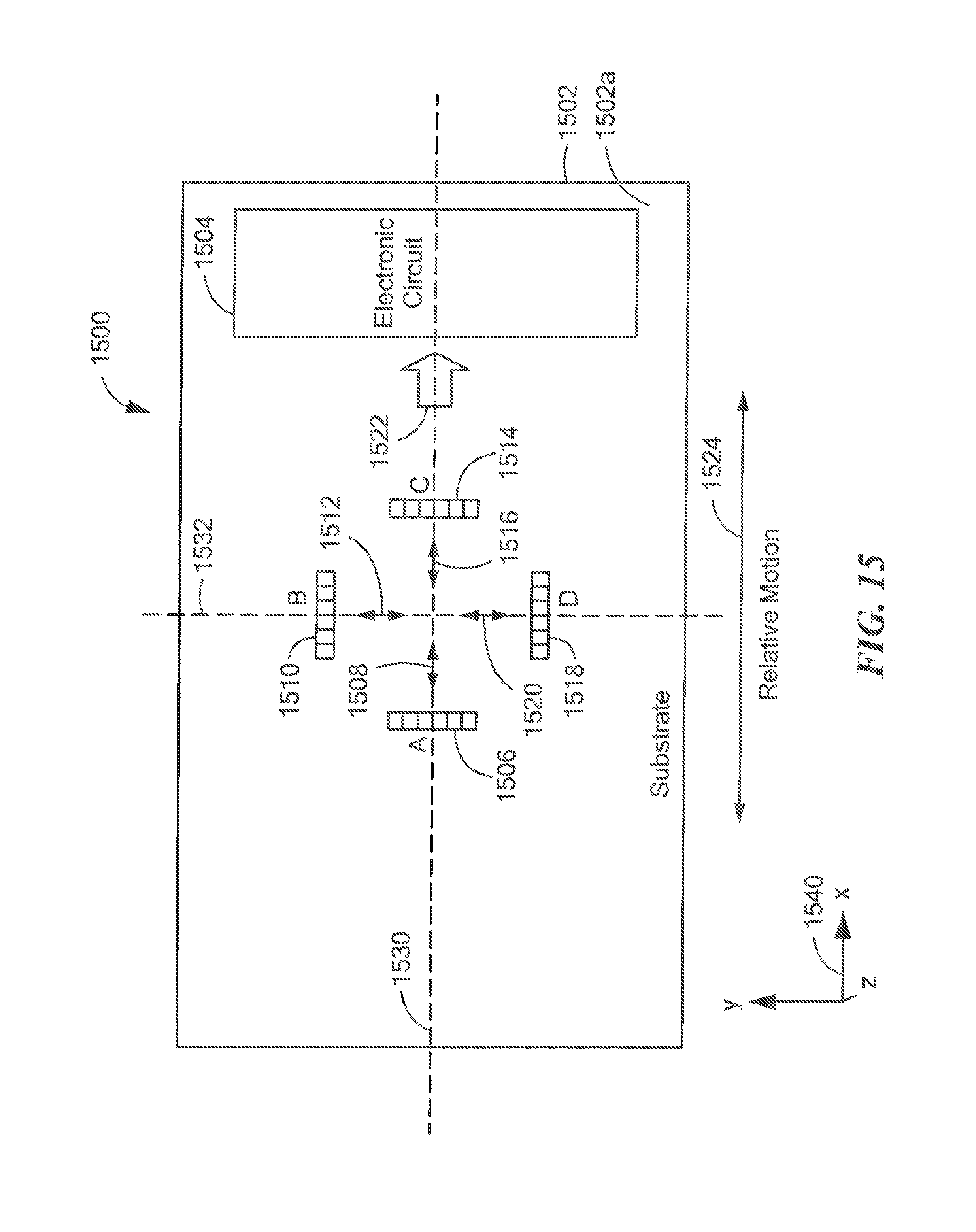
D00016
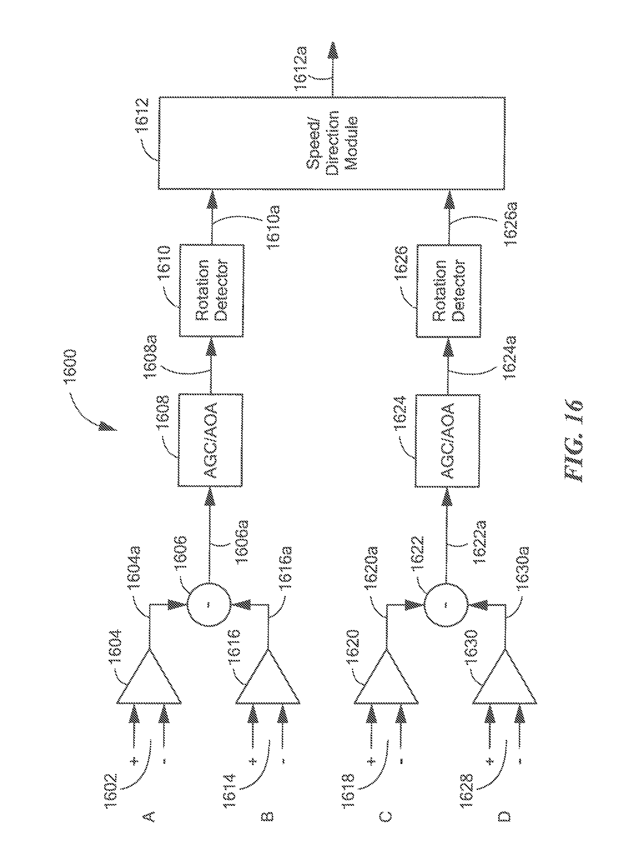
D00017
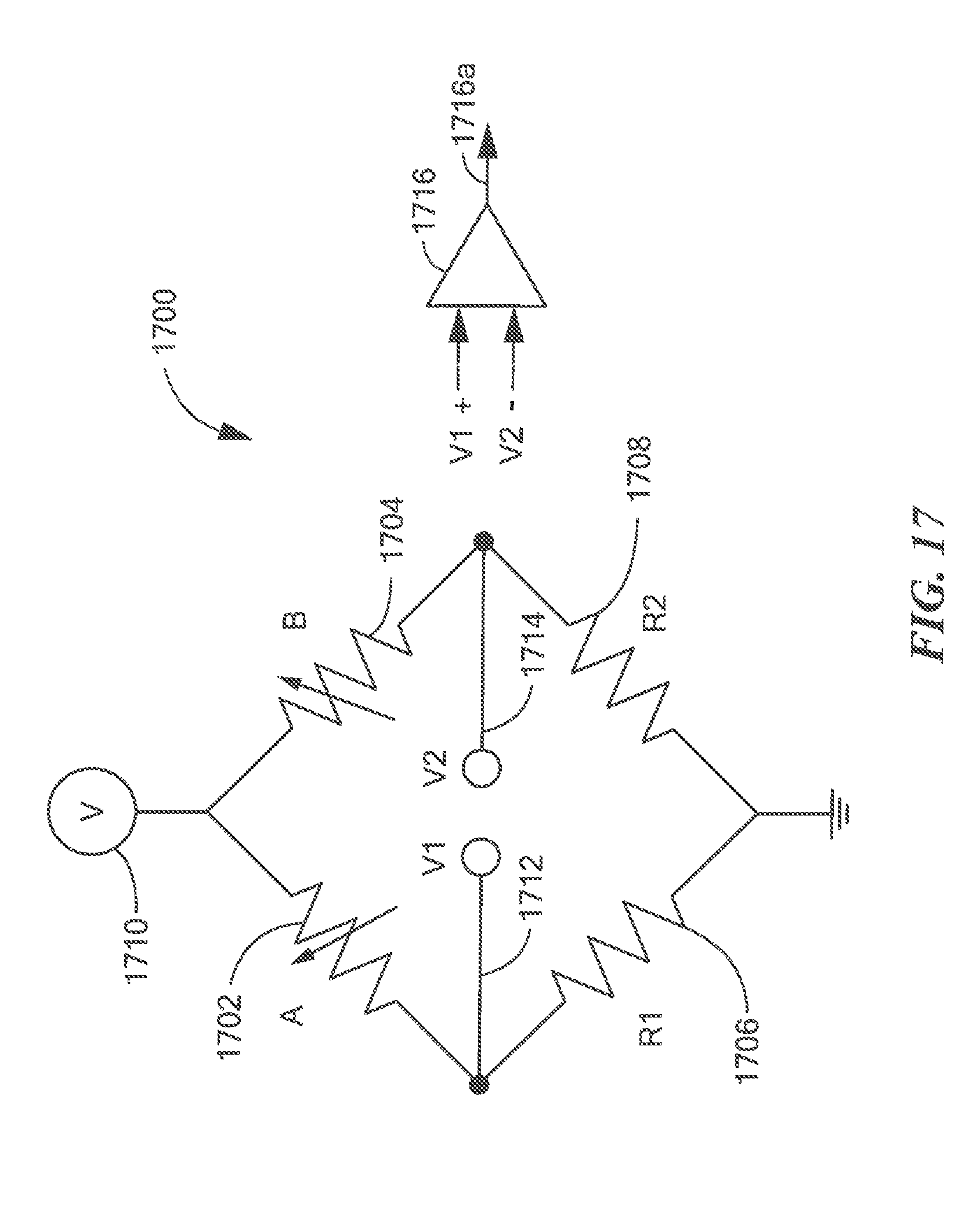
XML
uspto.report is an independent third-party trademark research tool that is not affiliated, endorsed, or sponsored by the United States Patent and Trademark Office (USPTO) or any other governmental organization. The information provided by uspto.report is based on publicly available data at the time of writing and is intended for informational purposes only.
While we strive to provide accurate and up-to-date information, we do not guarantee the accuracy, completeness, reliability, or suitability of the information displayed on this site. The use of this site is at your own risk. Any reliance you place on such information is therefore strictly at your own risk.
All official trademark data, including owner information, should be verified by visiting the official USPTO website at www.uspto.gov. This site is not intended to replace professional legal advice and should not be used as a substitute for consulting with a legal professional who is knowledgeable about trademark law.