Electromagnetic interference containment system
Frank , et al.
U.S. patent number 10,238,016 [Application Number 15/445,065] was granted by the patent office on 2019-03-19 for electromagnetic interference containment system. This patent grant is currently assigned to EMC IP Holding Company LLC. The grantee listed for this patent is EMC IP Holding Company LLC. Invention is credited to Christopher Frank, Timothy Olesiewicz, Clifford Willis.


| United States Patent | 10,238,016 |
| Frank , et al. | March 19, 2019 |
Electromagnetic interference containment system
Abstract
A chassis includes a flash module comprising a cover and an integrated connector, a metal stiffener, an electromagnetic interference (EMI) gasket, and a midplane. The flash module is connected to the midplane using the integrated connector, the integrated connector extends past the cover of the flash module, and, when the flash module is connected to the midplane, the cover of the flash module is in direct contact with the EMI gasket, in which the metal stiffener is interposed between the EMI gasket and the midplane.
| Inventors: | Frank; Christopher (San Jose, CA), Olesiewicz; Timothy (Dubin, CA), Willis; Clifford (Tracy, CA) | ||||||||||
|---|---|---|---|---|---|---|---|---|---|---|---|
| Applicant: |
|
||||||||||
| Assignee: | EMC IP Holding Company LLC
(Hopkinton, MA) |
||||||||||
| Family ID: | 56381855 | ||||||||||
| Appl. No.: | 15/445,065 | ||||||||||
| Filed: | February 28, 2017 |
Prior Publication Data
| Document Identifier | Publication Date | |
|---|---|---|
| US 20170172017 A1 | Jun 15, 2017 | |
Related U.S. Patent Documents
| Application Number | Filing Date | Patent Number | Issue Date | ||
|---|---|---|---|---|---|
| 14530631 | Oct 31, 2014 | 9622394 | |||
| 62005787 | May 30, 2014 | ||||
| Current U.S. Class: | 1/1 |
| Current CPC Class: | H05K 7/2039 (20130101); H05K 5/0026 (20130101); H05K 9/0015 (20130101); H05K 7/20563 (20130101); H05K 5/0021 (20130101); H05K 7/20136 (20130101); H05K 7/1424 (20130101); H05K 9/0081 (20130101); H05K 7/1445 (20130101); G06F 1/182 (20130101) |
| Current International Class: | H05K 9/00 (20060101); H05K 7/20 (20060101); H05K 7/14 (20060101); H05K 5/00 (20060101); G06F 1/18 (20060101) |
References Cited [Referenced By]
U.S. Patent Documents
| D257345 | October 1980 | Levy |
| D260881 | September 1981 | McKinsey et al. |
| 4648066 | March 1987 | Pitt |
| 5023754 | June 1991 | Aug |
| 5045960 | September 1991 | Eding |
| 5065321 | November 1991 | Bezos et al. |
| D332256 | January 1993 | Lewis |
| 5214550 | May 1993 | Chan |
| 5253129 | October 1993 | Blackborow et al. |
| 5297067 | March 1994 | Blackborow et al. |
| 5316488 | May 1994 | Gardner et al. |
| 5387115 | February 1995 | Kozel et al. |
| 5519573 | May 1996 | Cobb et al. |
| 5570270 | October 1996 | Naedel et al. |
| 5691860 | November 1997 | Hoppe |
| 5701894 | December 1997 | Cherry et al. |
| 5764480 | June 1998 | Crump et al. |
| 5825616 | October 1998 | Howell et al. |
| D408379 | April 1999 | McGraw et al. |
| 6083018 | July 2000 | Hara et al. |
| 6137759 | October 2000 | Ogiro et al. |
| 6174180 | January 2001 | Chen |
| 6185103 | February 2001 | Yamada |
| 6222727 | April 2001 | Wu |
| 6324062 | November 2001 | Treiber et al. |
| 6324075 | November 2001 | Unrein et al. |
| 6359778 | March 2002 | Wu |
| 6373696 | April 2002 | Bolognia et al. |
| 6388884 | May 2002 | Greco et al. |
| 6396704 | May 2002 | White |
| 6538903 | March 2003 | Radu |
| 6654235 | November 2003 | Imsand |
| 6683785 | January 2004 | Chen |
| 6987927 | January 2006 | Battaglia et al. |
| 7023704 | April 2006 | Zarnowitz et al. |
| 7042737 | May 2006 | Woolsey |
| 7088579 | August 2006 | Konshak |
| 7242576 | July 2007 | Coster et al. |
| 7251145 | July 2007 | Reznikov |
| 7362566 | April 2008 | Sivertsen |
| 7396244 | July 2008 | Barna et al. |
| 7499286 | March 2009 | Berke et al. |
| 7719855 | May 2010 | Berke et al. |
| 7944691 | May 2011 | Pounds |
| D698792 | February 2014 | Lin et al. |
| 8737067 | May 2014 | Kim et al. |
| 8760859 | June 2014 | Fuchs |
| 8897006 | November 2014 | Ito et al. |
| 8969816 | March 2015 | Caruba et al. |
| 9395772 | July 2016 | Degner et al. |
| 9622394 | April 2017 | Frank |
| 2002/0018423 | February 2002 | Goble |
| 2002/0030927 | March 2002 | Kimura et al. |
| 2002/0033890 | March 2002 | Nicklos et al. |
| 2002/0114254 | August 2002 | Ohgaki |
| 2002/0122295 | September 2002 | Laing |
| 2002/0169912 | November 2002 | Mills et al. |
| 2002/0182896 | December 2002 | Welsh et al. |
| 2003/0041203 | February 2003 | Jones et al. |
| 2003/0136849 | July 2003 | Adelmann |
| 2003/0161199 | August 2003 | Estakhri |
| 2004/0057702 | March 2004 | Battaglia et al. |
| 2004/0213141 | October 2004 | Lin |
| 2004/0228184 | November 2004 | Mathiowetz |
| 2004/0233629 | November 2004 | Wang et al. |
| 2004/0242041 | December 2004 | Ngo |
| 2005/0018397 | January 2005 | Kay et al. |
| 2005/0259395 | November 2005 | Espinoza-Ibarra et al. |
| 2006/0030080 | February 2006 | Hsueh et al. |
| 2006/0061955 | March 2006 | Imblum |
| 2006/0072239 | April 2006 | Iftikar |
| 2006/0146441 | July 2006 | Chih |
| 2007/0070669 | March 2007 | Tsem |
| 2007/0217171 | September 2007 | Le |
| 2007/0274039 | November 2007 | Hamlin |
| 2007/0293137 | December 2007 | Crippen et al. |
| 2008/0002348 | January 2008 | Kim et al. |
| 2008/0094799 | April 2008 | Zieman et al. |
| 2008/0112125 | May 2008 | Martin et al. |
| 2008/0218949 | September 2008 | Hughes |
| 2008/0218957 | September 2008 | Kim et al. |
| 2008/0225479 | September 2008 | Zieman et al. |
| 2008/0266779 | October 2008 | Thomas et al. |
| 2008/0298009 | December 2008 | Weng et al. |
| 2008/0298014 | December 2008 | Franco |
| 2008/0310107 | December 2008 | Vinson et al. |
| 2008/0316704 | December 2008 | Vinson et al. |
| 2009/0016019 | January 2009 | Bandholz et al. |
| 2009/0034349 | February 2009 | Miura |
| 2009/0086456 | April 2009 | Milo et al. |
| 2009/0100217 | April 2009 | Battaglia et al. |
| 2009/0109619 | April 2009 | Wise et al. |
| 2009/0135558 | May 2009 | Hughes |
| 2009/0147462 | June 2009 | Zhu et al. |
| 2009/0154098 | June 2009 | Nguyen |
| 2009/0172279 | July 2009 | Yuan et al. |
| 2009/0185355 | July 2009 | Zhu et al. |
| 2009/0198927 | August 2009 | Bondurant et al. |
| 2009/0210636 | August 2009 | Karamcheti et al. |
| 2009/0257191 | October 2009 | Ecker |
| 2009/0279243 | November 2009 | Amidi et al. |
| 2010/0002382 | January 2010 | Aybay et al. |
| 2010/0014248 | January 2010 | Boyden et al. |
| 2010/0142243 | June 2010 | Baxter |
| 2010/0323757 | December 2010 | Seflic et al. |
| 2010/0328886 | December 2010 | Nguyen |
| 2010/0332711 | December 2010 | Li et al. |
| 2011/0080701 | April 2011 | Bisson et al. |
| 2011/0153903 | June 2011 | Hinkle et al. |
| 2011/0222234 | September 2011 | Davis et al. |
| 2011/0261521 | October 2011 | Lo |
| 2011/0292588 | December 2011 | Seeley |
| 2012/0010754 | January 2012 | Matteson |
| 2012/0050986 | March 2012 | Riebel |
| 2012/0120596 | May 2012 | Bechtolsheim |
| 2012/0233402 | September 2012 | Laaksonen et al. |
| 2012/0278534 | November 2012 | Sun et al. |
| 2012/0327597 | December 2012 | Liu et al. |
| 2013/0054862 | February 2013 | Tsai |
| 2013/0107424 | May 2013 | Thomas et al. |
| 2013/0107443 | May 2013 | Kim et al. |
| 2013/0148287 | June 2013 | Chang |
| 2013/0163175 | June 2013 | Kim et al. |
| 2013/0176676 | July 2013 | Keffeler et al. |
| 2013/0176677 | July 2013 | Rust et al. |
| 2013/0342989 | December 2013 | Singleton |
| 2014/0078660 | March 2014 | Dondzik et al. |
| 2014/0087787 | March 2014 | Rivera-Sanchez |
| 102006016743 | Oct 2007 | DE | |||
| 1420623 | May 2004 | EP | |||
| 2275913 | Jan 2011 | EP | |||
| 06-309860 | Apr 1994 | JP | |||
| 03063560 | Jul 2003 | WO | |||
| 2005029936 | Mar 2005 | WO | |||
| 2007056669 | May 2007 | WO | |||
| 2008103359 | Aug 2008 | WO | |||
| 2009015285 | Jan 2009 | WO | |||
| 2013029264 | Mar 2013 | WO | |||
Other References
|
Press Release, "3M Introduces New CompactFlash brand Type II Card Ejectors for Long Guide CFII Headers," 3M News, www.3M.com, Jul. 6, 2006 (2 pages). cited by applicant . Doug Hoy, "Delphi Connection Systems Adds to Growing Portfolio with Introduction of PCI Express(TM), DDR2-DIMM Series; Computing Products' Availability Announced During Appearance at IDF.," PR Newswire, http://www.thefreelibrary.com/Delphi+Connection+Systems...s+to+Growing+Po- rtfolio+with+Intruction...-a0121678034, Sep. 7, 2004 (4 pages). cited by applicant . StarTech.com, "Removable 2.5'' SATA HDD Enclosure/Backup System/Mobile Rack for 3.5/5.25'' Bay", Product ID: SAT2510U3REM, http://www.startech.com/HDD/Mobile-Racks/Removable-Hard-Drive-Enclosure-B- ackup-System.about.SAT2510U3REM, date accessed Apr. 16, 2014 (3 pages). cited by applicant . PC Support Services Ltd., "The Saturn Mobile Rack", http://www.pcssl.co.nz/documents/prodinfo/addonics/Saturn%20and%20Cipher/- MobileRack.htm, dated accessed Apr. 16, 2014 (5 pages). cited by applicant . ICY DOCK, "EZ-Fit MB990SP-B Tool-less Dual 2.5'' SSD/HDD Mounting Kit / Bracket", http://www.icydock.com/goods.php?id=79, date accessed Apr. 16, 2014 (3 pages). cited by applicant . "Removable Memory Cartridge Houses 2.5-Inch SATA Drives", http://www.cotsjournalonline.com/articles/view/103844, date accessed Apr. 16, 2014 (1 page). cited by applicant . Tapeonline.com, "Imation RDX 500GB Removable Cartridge", http://www.tapeonline.com/products/imation-rdx-rdx-500gb-removable-cartri- dge, date accessed Apr. 16, 2014 (2 pages). cited by applicant . "Quantum RDX", Quantum Datasheet, http://www.quantum.com/products/removablediskdrives/rdx/index.aspx, date accessed Apr. 16, 2014 (2 pages). cited by applicant . Plastiras, Elias, "HP Z1 workstation (B4F79PA) review", PC World, http://www.pcworld.idg.com.au/review/hp/z1_workstation_b4f79pa_review/426- 935/, Jul. 6, 2012 (12 pages). cited by applicant . "CWC Debuts Low-Cost Rugged, Removable Solid State Memory Module Carrier", http://www.unmannedsystemstechnology.com/2013/12/cwc-debuts-low-cost-rugg- ed-removable-solid-state-memory-module-carrier/, dated Dec. 19, 2013 (2 pages). cited by applicant . Curtiss-Wright, "Curtiss-Wright Acquired Parvus Corporation, Extends Curtiss-Wright's Capabilities in Rugged Small Form Factor Computing and Communications Subsystems", http://www.parvus.com/product/overview.aspx?prod=RuggedRemovableMassStora- ge, date accessed Apr. 15, 2014 (2 pages). cited by applicant . Curtiss-Wright, Press Release, "Curtiss-Wright Controls Introduces Rugged Cartridges for Standard High-Density SATA Solid State Drives", http://news.thomasnet.com/fullstory/Rugged-Cartridges-facilitate-removeab- le-SATA-SSD-deployment-20019299, dated Dec. 12, 2013 (7 pages). cited by applicant . Synchrotech, "PCMCIA ATA Flash PC Cards FMJ Industrial", http://www.synchrotech.com/products/ata-flash-pcmcia-memory-pc_cards_12-f- mj-industrial.html, date accessed Apr. 15, 2014 (2 pages). cited by applicant . Molex, "CompactFlash.TM.", http://www.molex.com/molex/products/family?channel=products&chanName=fami- ly&key=compactflash, date accessed Apr. 15, 2014 (5 pages). cited by applicant. |
Primary Examiner: Hoffberg; Robert J
Assistant Examiner: Dang; Hung
Attorney, Agent or Firm: Chamberlain, Hrdlicka, White, Williams & Aughtry
Parent Case Text
CROSS-REFERENCE TO RELATED APPLICATIONS
Pursuant to 35 U.S.C. .sctn. 119(e), this application claims benefit of U.S. Provisional Application No. 62/005,787 filed on May 30, 2014, entitled "STORAGE ASSEMBLY SYSTEM." The disclosure of the U.S. Provisional Application is incorporated herein by reference in its entirety.
Claims
What is claimed is:
1. An electromagnetic interference (EMI) containment system, comprising: a chassis, comprising: a front section, comprising: a module bay configured to accommodate a plurality of removably insertable flash modules; a rear section that is EMI contained; and a separation section that separates the front section from the rear section, the separation section comprising: a metal stiffener, comprising: a first plurality of openings, configured to enable airflow between the module bay and the rear section; and a second plurality of openings; and a midplane printed circuit board (PCB), disposed between the metal stiffener and the rear section, the midplane PCB having a plurality of holes, each of the holes corresponding to a respective opening of the first plurality of openings to enable the airflow between the module bay and the rear section; at least one flash module of the plurality of removably insertable flash modules, disposed within the module bay, the at least one flash module comprising: a cover providing EMI containment to flash module circuits; and a connector that extends beyond the cover, wherein upon insertion of the at least one flash module into the module bay: the connector interfaces with the midplane PCB, through at least one of the second plurality of openings, and the connector is EMI contained.
2. The chassis of claim 1, wherein the cover of the flash module provides heat dissipation to the flash module circuits.
3. The chassis of claim 2, wherein the airflow removes heat from the cover while traversing through the module bay.
4. The chassis of claim 2, wherein the airflow removes heat from the midplane PCB.
5. A chassis that does not provide chassis level electromagnetic interference (EMI) containment, the chassis comprising: a module bay that does not provide EMI containment for flash modules disposed in the module bay; a rear section that does provide EMI containment for elements disposed in the rear section; a metal stiffener disposed between the module bay and the rear section, the metal stiffener comprising: a first plurality of holes that enables an airflow between the module bay and the rear section; and a second plurality of holes, wherein each hole of the second plurality of holes is configured to: receive a flash module of the flash modules, and form an electromagnetic seal between the metal stiffener and the flash module; and a midplane printed circuit board (PCB), disposed between the metal stiffener and the rear section, the midplane PCB having a plurality of holes, each of the holes corresponding to a respective hole of the first plurality of holes, enabling the airflow between the module bay and the rear section, wherein forming the electromagnetic seal provides the EMI containment for the flash module within the module bay.
6. The chassis of claim 5, wherein the rear section provides front EMI containment on a side of the rear section proximate to the metal stiffener, and wherein the airflow passes through the metal stiffener.
7. The chassis of claim 5, wherein the metal stiffener and a cover of the flash module provide the EMI containment of the flash module, and the module bay allows airflow to pass therethrough.
8. The chassis of claim 7, wherein the module bay does not provide front EMI containment, wherein the airflow passes through a front opening of the module bay.
9. The chassis of claim 5, wherein the module bay comprises a front opening that does not provide EMI containment, the front opening opposite to the metal stiffener.
Description
BACKGROUND
Storage assembly systems may include a chassis to house various components of the system. In particular, a storage assembly system may include components such a flash modules and printed circuit boards. These components may experience electromagnetic interference (EMI) unless these components are properly shielded.
BRIEF DESCRIPTION OF DRAWINGS
FIG. 1A shows a perspective view of a storage assembly in accordance with embodiments of the invention.
FIG. 1B shows a perspective view of a storage assembly in accordance with embodiments of the invention.
FIG. 2 shows an exploded view of a flash module in accordance with embodiments of the invention.
FIG. 3 shows a front view of the storage assembly system in accordance with one or more embodiments of the invention.
FIGS. 4-5 show side views of the storage assembly system in accordance with one or more embodiments of the invention.
FIG. 6 shows a detailed section view of the storage assembly system in accordance with one or more embodiments of the invention.
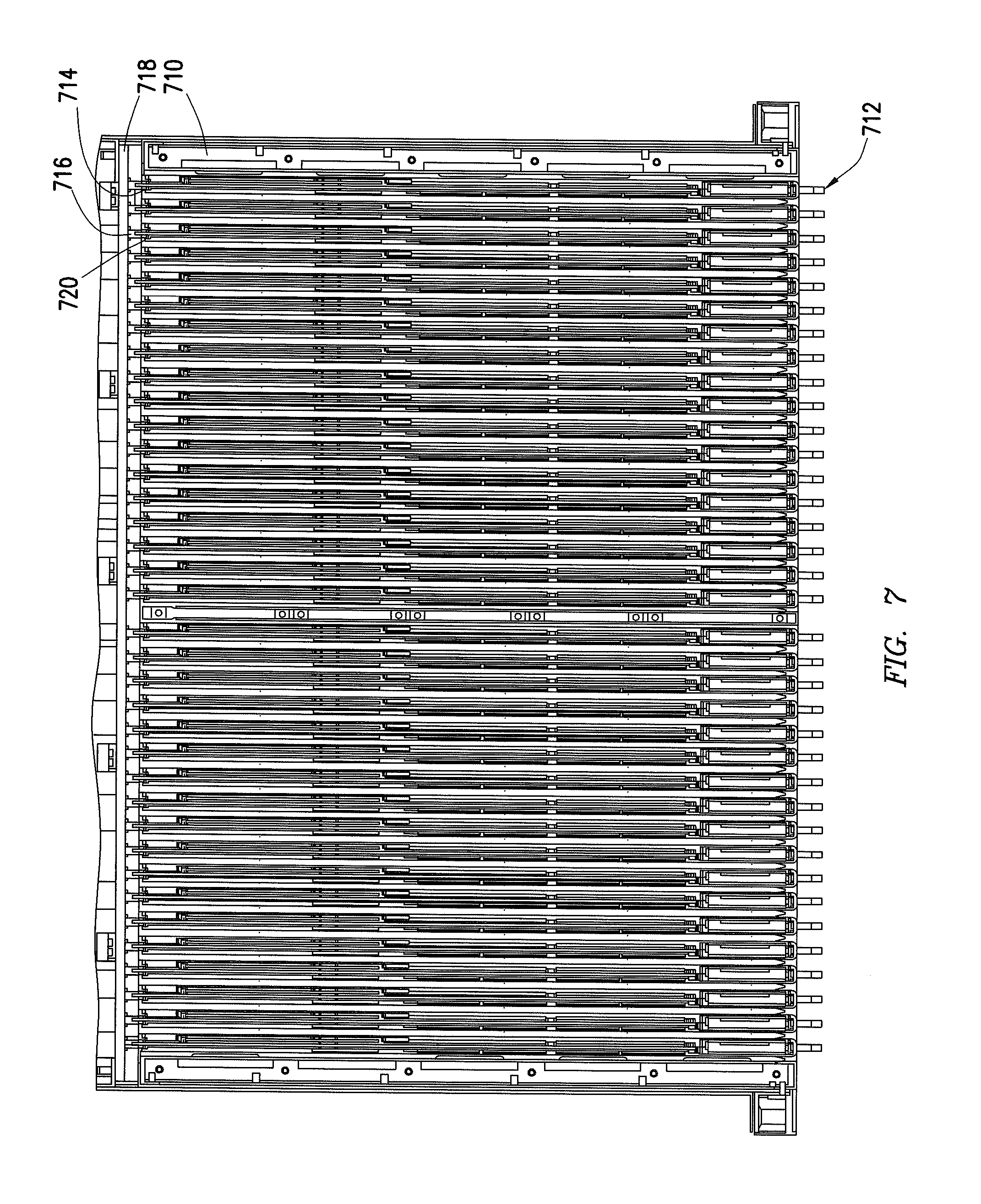
FIG. 7 shows a top view of the storage assembly system in accordance with one or more embodiments of the invention.
FIG. 8 shows a detailed top view of the storage assembly system in accordance with one or more embodiments of the invention.
FIG. 9 shows a front view of the storage assembly system in accordance with one or more embodiments of the invention.
DETAILED DESCRIPTION
Specific embodiments of the invention will now be described in detail with reference to the accompanying figures. In the following detailed description of embodiments of the invention, numerous specific details are set forth in order to provide a more thorough understanding of the invention. However, it will be apparent to one of ordinary skill in the art that the invention may be practiced without these specific details. In other instances, well-known features have not been described in detail to avoid unnecessarily complicating the description.
In the following description of FIGS. 1-9, any component described with regard to a figure, in various embodiments of the invention, may be equivalent to one or more like-named components described with regard to any other figure. For brevity, descriptions of these components will not be repeated with regard to each figure. Thus, each and every embodiment of the components of each figure is incorporated by reference and assumed to be optionally present within every other figure having one or more like-named components. Additionally, in accordance with various embodiments of the invention, any description of the components of a figure is to be interpreted as an optional embodiment which may be implemented in addition to, in conjunction with, or in place of the embodiments described with regard to a corresponding like-named component in any other figure.
In one aspect, embodiments disclosed herein relate generally to a chassis of a storage assembly system. More specifically, one or more embodiments disclosed herein may be directed to one or more components of a chassis of a storage assembly system. For example, one or more embodiments disclosed herein relate to chassis having an EMI gasket that is configured to contact a cover of a flash module when the flash module is mounted on the chassis. Further, one or more embodiments disclosed herein relate to a flash module having a cover, in which the cover provides EMI shielding for the flash module. EMI may be considered a disturbance that may affect an electrical circuit due to induction or radiation from an external electromagnetic source. Such a disturbance may limit or negatively affect the performance of the circuit and may potentially lead to the loss of data.
Although one or more of these embodiments may be preferred, the embodiments disclosed should not be interpreted, or otherwise used, as limiting the scope of the disclosure, including the claims. In addition, those skilled in the art will appreciate that the following description has broad application, and the discussion of any embodiment is meant only to be exemplary of that embodiment, and not intended to suggest that the scope of the disclosure, including the claims, is limited to that embodiment.
Certain terms are used throughout the following description and claims to refer to particular features or components. As those skilled in the art will appreciate, different persons may refer to the same feature or component by different names. This document does not intend to distinguish between components or features that differ in name but not function. The figures are not necessarily to scale. Certain features and components herein may be shown exaggerated in scale or in somewhat schematic form and some details of conventional elements may not be shown in interest of clarity and conciseness.
In the following discussion and in the claims, the terms "including" and "comprising" are used in an open-ended fashion, and thus should be interpreted to mean "including, but not limited to . . . " Also, the term "couple" or "couples" is intended to mean either an indirect or direct connection. Thus, if a first component is coupled to a second component, that connection may be through a direct connection, or through an indirect connection via other components, devices, and connections.
One or more aspects of the present disclosure are directed to a storage assembly system. Referring to FIGS. 1A and 1B, multiple perspective views of a storage assembly system 106 in accordance with embodiments disclosed herein are shown.
In one or more embodiments, the storage assembly system (106) may include a chassis (101), in which one or more components may be disposed and secured within. For example, as shown in FIG. 1B, one or more flash modules (109) are disposed within a front portion of the chassis (101). In one or more embodiments, the one or more flash modules (109) may be engaged within the chassis (101) of the storage assembly system (106).
Further, as shown, one or more openings may be formed through the chassis (101) of the storage assembly system (106), where the one or more openings may permit airflow through the chassis (101) of the storage assembly system (106). In one or more embodiments, the aforementioned openings formed through the chassis (101) may include an upper airflow chamber (110), a central airflow chamber (111), and a lower airflow chamber (112). In one or more embodiments, structural arrangement of one or more internal components may allow airflow to be controllably directed from each of the upper airflow chamber (110) and the lower airflow chamber (112) into the central airflow chamber (111). In one embodiment of the invention, the chassis (101) further includes a vent (113) that may allow airflow through the chassis (101).
In one or more embodiments, the one or more flash modules (109) may be spaced apart when engaged within the chassis (101) of the storage assembly system (106) to allow airflow between one or more flash modules (109) into an interior of the chassis (101).
As shown in FIG. 1B, the storage assembly (100) includes the chassis (101) and the upper airflow chamber (110), the central airflow chamber (111), and the lower airflow chamber (112). A fan module (not shown) may be used to pull air through each of the upper airflow chamber (110), the central airflow chamber (111), and the lower airflow chamber (112.
FIG. 2 shows an exploded view of a flash module in accordance with one or more embodiments of the invention. The flash module includes a top cover (200) and a bottom cover (210). The top cover (200) is in direct contact with a thermal interface material (TIM) (202A). In one embodiment of the invention, the TIM is a malleable material such as a silicon-based putty or gel. Other TIMs may be used without departing from the invention. The TIM (202A) is also in direct contact with all (or substantially all or a significant portion of) the components on the top surface of the printed circuit board (PCB) (204). For example, the TIM (202A) is in direct contact with the solid state storage (236) and the memory (238). The TIM (202A), in one or more embodiments of the invention, is positioned within the flash module as to limit the air gaps between the components on the top surface of the PCB and the TIM (202A). Further, in one or more embodiments, the TIM material (e.g., TIM (202A) and/or TIM (202B)) may fill a gap or space between PCB components and a cover (e.g., the top cover (200) and/or the bottom cover (210)) of the flash module.
In one embodiment of the invention, solid state storage may include, but is not limited to, NAND Flash memory, NOR Flash memory, Magnetic RAM Memory (MRAM), Spin Torque Magnetic RAM Memory (ST-MRAM), Phase Change Memory (PCM), memristive memory, or any other memory defined as a non-volatile Storage Class Memory (SCM). Those skilled in the art will appreciate that embodiments of the invention are not limited to storage class memory.
In one embodiment of the invention, the memory (238) corresponds to any volatile memory including, but not limited to, Dynamic Random-Access Memory (DRAM), Synchronous DRAM, SDR SDRAM, and DDR SDRAM.
In one embodiment of the invention, the TIM (202A) does not extend over the super capacitor assembly (206), the cable assembly (208) that connects the PCB (204) to the super capacitor assembly (206), or the latch assembly (212).
In one embodiment of the invention, the super capacitor assembly (206) includes a super capacitor enclosed in an insulator, e.g., a plastic insulator. The insulator surrounding the super capacitor is in direct contact with the top cover (200) and the bottom cover (210). The flash module includes a controller (or series of controllers) (e.g., a hot-swap controller) that is configured to monitor voltage drops across the flash module. This functionality allows the flash module to detect when it is disconnected from a midplane of the chassis of a storage assembly. When the flash module is disconnected from the midplane, the components on the flash module (including components on the PCB) continue to receive power for a period of time in order to ensure that all data that is currently stored in the memory (or all data in memory that needs to be persistently stored) (238) is stored in solid state storage on the flash module. This functionality may ensure that no data is lost when the flash module is disconnected from power (e.g., disconnected from the midplane). The super capacitor is sized to ensure that there is sufficient power to enable the aforementioned functionality. The super capacitor may be included within a cavity (218) within the bottom cover (210).
In one embodiment of the invention, solid state storage is mounted on both the top surface of the PCB (see e.g., solid state storage (204)) and the bottom surface of the PCB. In one embodiment of the invention, the total storage capacity of the solid state storage in a given flash module is between 2 TB-16 TB.
In one embodiment of the invention, the memory (see e.g., memory (238)) is mounted on both the top surface of the PCB and the bottom surface of the PCB. In one embodiment of the invention, the total storage capacity of the memory in a given flash module is between 2-4GB. The invention is not limited to the aforementioned memory size range. In one embodiment of the invention, the ratio of the storage capacity of the memory to the storage capacity of the solid state storage is 1:1000. The invention is not limited to the aforementioned ratio.
In one embodiment of the invention, the top and bottom covers of the flash module are made of Aluminum. However, those skilled in the art will appreciate that they may be made of any other material that functions to (i) dissipate heat and/or (ii) shield the internal components in the flash module from electromagnetic interference (EMI). In one embodiment of the invention, the top and bottom covers of the flash module act as heat sinks. The top and bottom covers may be made of other materials such as composites, alloys, or any other material that has high thermal conductivity. The selection of a specific material for the top and bottom cover of the flash module may vary based on the amount of heat the needs to be removed from the flash module. Further, while the flash module is described using a single material for the top and bottom covers, the top and bottom covers of the flash module may be made of different materials. Further, the materials used for a given cover may also be non-uniform such that one portion of a cover may be made of a first material and a second portion of the cover may be made of a second material.
In one embodiment of the invention, the PCB is attached to the bottom cover (210) via screws (e.g., 226A, 226B, 226C, and 226D).
In one embodiment of the invention, a heat spreader (234) is located between the bottom cover (210) and the TIM (202B). The heat spreader (234) may be made of any material that provides efficient heat dissipation in order to prevent any hotspots on the bottom cover as a result of the heat generated by the storage controller that is mounted on the bottom surface of the PCB. The heat spreader (234) may be made of, for example, carbon fiber. The heat spreader may use other materials without departing from the invention. The heat spreader (234) may be located in a cavity (222) within the bottom cover (210). The TIM (202B) is in direct contact with the heat spreader (222). The TIM (202B) may not be in contact with the latch assembly (212) or the super capacitor (206).
In one embodiment of the invention, the storage controller includes functionality to service read requests to read data from the solid state storage and/or to service write requests to write data to the solid state storage. The storage controller includes a single or multi-channel architecture to access the memory (238). Further, the storage controller may implement and/or support single data rate (SDR), double data rate (DDR), and/or Quad data rate (QDR) transfers.
The TIM (202B) may be in direct contact with all (or substantially all or a significant portion of) the components on the bottom surface of the printed circuit board (PCB) (204). For example, the TIM (202B) may be in direct contact with the solid state storage and the memory. The TIM (202B), in one or more embodiments of the invention, is positioned within the flash module as to limit the air gaps between the components on the bottom surface of the PCB and the cover (210).
The flash module may include a bezel (230) that connects to the top and bottom covers (200, 210) of the flash module. The bezel (230) may include a hole (228) through which a handle (216) may be inserted, where the handle (216) is part of the latch assembly (212). The bezel may also have a flat surface (214) that includes one or more indicator lights. The bezel may have a different geometry as compared to what is shown in FIG. 2 without departing from the invention. The bezel (230) may be positioned within the flash module using, e.g., a pin (222A), and may further be secured to the flash module using a screw (242).
The top and bottom covers of the flash module may be connected together by press fitting. Said another way, the top and bottom covers are pressed together to create the flash module. In such cases, there are no external fasteners are used to connect the top and bottom covers of the flash modules to each other. The lack of external fasteners may enable the flash module to be tamper resistant. In other embodiments of the invention, the top and bottom covers may be connected together using external fasteners including, but not limited to, screws, pins, epoxy (or other adhesive chemical compounds).
In one embodiment of the invention, the flash module is hot-swappable. This functionality is implemented by a hot-swap controller that is attached to either the top or bottom of the PCB. The hot-swap controller may be an implemented, using a general purpose processor, an application-specific integrated circuit (ASIC), a Field Programmable Gate Array (FPGA), or any other integrated circuit. In one embodiment of the invention, when the flash module is disconnected from the midplane, the hot-swap controller electrically isolates the flash module from the midplane and other components connected thereto. This enables all power that is discharged from the super capacitor to be used only to power the flash module and not to power other components external to the flash module.
The flash module may include an indictor (232) that includes one or more light emitting diodes (LEDs) (or other light sources). The LEDs may include provide a visual indication of the status and/or whether the flash module is powered on. The
LEDs may provide other status information without departing from the invention. The indicator (232) may receive power and signal information via a flex circuit (224).
Though not shown in FIG. 2, the indicator (232) may also include a mechanical switch that interfaces with the latch assembly (212). When the handle (216) is pulled outward in order to remove the flash module from the chassis, the mechanical switch will be displaced (or otherwise moved) resulting in a signal being sent to the storage controller. The storage controller, upon receipt of the signal, triggers the transfer of all or a portion of the data currently stored in the memory (e.g., 238) to the solid state storage (236). The aforementioned mechanism may allow the storage controller additional time to transfer data from the memory to the solid state storage prior to the flash module being disconnected from the midplane. Once the flash module is disconnected from the midplane, components the flash module may continue to receive power from the super capacitor (described above) (206). In one embodiment of the invention, the mechanical switch may be implemented in embodiments in which the super capacitor is not able to discharge sufficient power, i.e., the super capacitor is not able to power the flash module for a period of time that is sufficient to ensure that all data (or all data that needs to be persistently stored) that is currently stored in the memory (238) is stored in solid state storage on the flash module.
In one embodiment of the invention, the flash module has the following dimensions: 80 mm.times.8.5 mm.times.304 mm (H.times.W.times.D). The flash module is not limited to the aforementioned dimensions. The depth of the flash module may correspond to the distance between the front portion of the chassis and the midplane. The flash module width may be designed such that 36 flash modules can be concurrently inserted within a chassis. The height of the flash module may be 2 U (or substantially 2 U).
The flash module also includes two 4.times. Peripheral Component Interconnect Express (PCIe) connectors (240). The two 4.times. PCIe connectors enable the flash module to connect to the midplane. Once a flash module is connected to the midplane the flash module may communicate via the midplane with one or more other components that are also connected to the midplane.
In other embodiments of the invention the flash module may implement connectors that conform with one or more of the following protocols: Peripheral Component Interconnect (PCI), PCI-eXtended (PCI-X), Non-Volatile Memory Express (NVMe), Non-Volatile Memory Express (NVMe) over a PCI-Express fabric, Non-Volatile Memory Express (NVMe) over an Ethernet fabric, and Non-Volatile Memory Express (NVMe) over an Infiniband fabric. Those skilled in the art will appreciate that the invention is not limited to the aforementioned protocols.
While the above description indicates that screws are used to affix the PCB to the bottom cover of the flash module, other connecting means may be used in place of screws. The other connecting means may include pins, epoxy, springs, or other physical components or adhesive chemical compounds that may be used to affix the PCB to the bottom cover within the flash module.
Though not described above, those skilled in the art will appreciate that the PCB may include other components mounted thereon.
FIG. 3 shows a front view of the storage assembly system in accordance with one or more embodiments of the invention. The storage assembly system (also referred to as a chassis) includes front face electromagnetic interface (EMI) containment in sections denoted (310). The front face EMI containment may be implemented using metal screens, metal meshes, etc, which may enable air to flow there through. The chassis implements rear face EMI containment in section (312), i.e., the section in which the flash modules are inserted. The absence of the front face EMI containment in section (312) permits air to flow across the top and bottom covers of the flash modules. Further, while there is no chassis level EMI containment across the front of section (312), each of the individual flash modules includes its own individual EMI containment (namely the top cover, bottom cover, and bezel).
FIGS. 4-5 show side views of the storage assembly system in accordance with one or more embodiments of the invention. Referring to FIG. 4, EMI containment for sections 310 in FIG. 3 may include EMI gaskets (410) located at or near the perimeter of the chassis. As previously discussed, the flash module cover (412) provides essentially complete EMI containment for the flash module expect for a small region at the rear portion of the flash module where the PCIe connectors extend past the end of the top and bottom cover of the flash module (see e.g., FIG. 2, PCIe connector (240)). EMI containment on the each of the flash modules may be achieved using an EMI gasket (414). The EMI gasket may be any suitable material including foams, gels, or any other material and/or compound that is suitable to serve as a gasket for EMI containment. Referring to FIG. 5, when the flash module is plugged-in (or otherwise connected) to the midplane, the ends of the flash module covers from the which the PCIe connectors extend are in contact with the EMI gasket (e.g., the EMI gasket (414) shown in FIG. 4) thereby extending the EMI containment (e.g., in the form of a Faraday Cage) to the midplane, thus establishing a complete enclosure which includes electrically conductive solid materials and/or meshes. The components inside the faraday cage, such as the flash module components shown in FIG. 2 and including the PCIe connectors, are thus protected from external electrical fields.
A metal stiffener (512) is located between the flash modules and the midplane. The metal stiffener (512) shields the rest of the chassis from the module bay (i.e., the portion of the chassis in which the flash modules are inserted). The metal stiffener (512) may include ventilation holes that enable thermal cooling of the flash modules. The absence of EMI gaskets within the front face of the chassis in section 312 (in FIG. 3) may enable improved airflow through the module bay.
FIG. 6 shows a detailed section view of the storage assembly system in accordance with one or more embodiments of the invention. When inserted into the midplane (618), the PCIe connectors are shrouded by the flash module covers and the metal stiffener (616) thereby providing EMI containment for the flash module and also for the module bay (discussed above). The EMI gaskets (612) are interposed between the flash module and the metal stiffener in order to close any gaps between the flash module and the metal stiffener. The metal stiffener (616) may be Aluminum (or any other material that may be used to EMI containment) The metal stiffener (616) may also include one or more holes (610) to permit airflow from the module bay to the rear portion of the chassis.
FIG. 7 shows a top view of the storage assembly system in accordance with one or more embodiments of the invention. FIG. 7 shows the placement of 36 flash modules (712) within the chassis (710). Further, the PCIe connectors of each of the flash modules are connected, via the holes (716) within the metal stiffener and EMI gasket, to the midplane (718). An EMI gasket (720) and metal stiffener (714) are interposed between the midplane and the flash modules.
FIG. 8 shows a detailed top view of the storage assembly system in accordance with one or more embodiments of the invention. Referring to FIG. 8, air (818) may pass through the spaces between the flash modules (816). The absence of EMI gaskets between the flash modules enables air to flow across the surface of the flash modules, thereby enable cooling of the flash modules. As shown in FIG. 8, the flash modules are connected to the midplane (810). The miplane (or portions thereof) are covered with a metal stiffener (812). Finally, an EMI gasket (814) covers at least a portion of the metal stiffener.
FIG. 9 shows a front view of the storage assembly system in accordance with one or more embodiments of the invention. Referring in FIG. 9, the midplane includes module connectors (910) at which the PCIe connectors are configured to interface. A metal stiffener (912) is included in front of the midplane and includes numerous holes (916) to permit air flow there through and holes to permit the PCIe connector to pass through. Finally, an EMI gasket(s) (914) is placed on the metal stiffener around the holes in the metal stiffener through which the PCIe connector passes through. In one or more embodiments, the EMI containment solutions discussed herein with regard to the chassis (e.g., the chassis 101) and one or more flash modules (e.g., the flash module shown in FIG. 2), may provide EMI containment while also allowing air flow through the front portion of the chassis and out the rear portion of the chassis. Further, in one or more embodiments, each of the flash modules discussed herein may be a Faraday Cage. Further, in one or more embodiments, the chassis itself according to embodiments disclosed herein may be a Faraday Cage (199).
While the disclosure includes a limited number of embodiments, those skilled in the art, having benefit of this disclosure, will appreciate that other embodiments may be devised which do not depart from the scope of the disclosure. Although only a few example embodiments have been described in detail above, those skilled in the art will readily appreciate that many modifications are possible in the example embodiments without materially departing from this invention. Accordingly, all such modifications are intended to be included within the scope of this disclosure.
* * * * *
References
-
3M.com
-
thefreelibrary.com/Delphi+Connection+Systems...s+to+Growing+Portfolio+with+Intruction...-a0121678034
-
startech.com/HDD/Mobile-Racks/Removable-Hard-Drive-Enclosure-Backup-System.about.SAT2510U3REM
-
pcssl.co.nz/documents/prodinfo/addonics/Saturn%20and%20Cipher/MobileRack.htm
-
icydock.com/goods.php?id=79
-
cotsjournalonline.com/articles/view/103844
-
tapeonline.com/products/imation-rdx-rdx-500gb-removable-cartridge
-
quantum.com/products/removablediskdrives/rdx/index.aspx
-
pcworld.idg.com.au/review/hp/z1_workstation_b4f79pa_review/426935
-
unmannedsystemstechnology.com/2013/12/cwc-debuts-low-cost-rugged-removable-solid-state-memory-module-carrier
-
parvus.com/product/overview.aspx?prod=RuggedRemovableMassStorage
-
news.thomasnet.com/fullstory/Rugged-Cartridges-facilitate-removeable-SATA-SSD-deployment-20019299
-
synchrotech.com/products/ata-flash-pcmcia-memory-pc_cards_12-fmj-industrial.html
-
molex.com/molex/products/family?channel=products&chanName=family&key=compactflash
D00000
D00001
D00002
D00003
D00004
D00005
D00006
D00007
D00008
D00009
D00010
XML
uspto.report is an independent third-party trademark research tool that is not affiliated, endorsed, or sponsored by the United States Patent and Trademark Office (USPTO) or any other governmental organization. The information provided by uspto.report is based on publicly available data at the time of writing and is intended for informational purposes only.
While we strive to provide accurate and up-to-date information, we do not guarantee the accuracy, completeness, reliability, or suitability of the information displayed on this site. The use of this site is at your own risk. Any reliance you place on such information is therefore strictly at your own risk.
All official trademark data, including owner information, should be verified by visiting the official USPTO website at www.uspto.gov. This site is not intended to replace professional legal advice and should not be used as a substitute for consulting with a legal professional who is knowledgeable about trademark law.