Imaging system
Gong
U.S. patent number 10,237,520 [Application Number 15/782,821] was granted by the patent office on 2019-03-19 for imaging system. This patent grant is currently assigned to UNION OPTECH CO., LTD.. The grantee listed for this patent is UNION OPTECH CO., LTD.. Invention is credited to Junqiang Gong.


| United States Patent | 10,237,520 |
| Gong | March 19, 2019 |
Imaging system
Abstract
The present invention discloses an imaging system, including an optical lens, where a spectroscopical module that can split a light wave transmitted from the optical lens into three light waves in different wavelength ranges is disposed on an imaging side of the optical lens; and the imaging system further includes three photosensitive chips configured to receive corresponding light waves, where the three photosensitive chips are correspondingly distributed at three light waves emitted by the spectroscopical module, and the spectroscopical module is a prism. In the present invention, a spectroscopical module is used to separate light whose wavelengths are different, and therefore light waves that are output from the spectroscopical module are three light waves in different wavelength ranges. These light waves in the different wavelength ranges are separately received by three different photosensitive chips. Therefore, each separate photosensitive chip receives a light wave whose wavelength range is relatively narrow.
| Inventors: | Gong; Junqiang (Guangdong, CN) | ||||||||||
|---|---|---|---|---|---|---|---|---|---|---|---|
| Applicant: |
|
||||||||||
| Assignee: | UNION OPTECH CO., LTD.
(Zhongshan, CN) |
||||||||||
| Family ID: | 59719425 | ||||||||||
| Appl. No.: | 15/782,821 | ||||||||||
| Filed: | October 12, 2017 |
Prior Publication Data
| Document Identifier | Publication Date | |
|---|---|---|
| US 20180376113 A1 | Dec 27, 2018 | |
Foreign Application Priority Data
| Jun 23, 2017 [CN] | 2017 1 0484286 | |||
| Current U.S. Class: | 1/1 |
| Current CPC Class: | G02B 27/145 (20130101); H04N 5/2254 (20130101); G02B 5/04 (20130101); H04N 9/097 (20130101); G01J 1/00 (20130101); G01J 3/513 (20130101); H04N 9/045 (20130101); G01J 3/2823 (20130101); G02B 27/1013 (20130101); G01J 3/0205 (20130101) |
| Current International Class: | G02B 5/04 (20060101); H04N 5/225 (20060101); H04N 9/04 (20060101); H04N 9/097 (20060101) |
| Field of Search: | ;348/337 |
References Cited [Referenced By]
U.S. Patent Documents
| 8520138 | August 2013 | Seale |
| 9675236 | June 2017 | McDowall |
| 2007/0146700 | June 2007 | Kowarz |
| 2007/0146710 | June 2007 | Kowarz |
| 2014/0092282 | April 2014 | Morishita |
| 2014/0347547 | November 2014 | Yatsuri |
| 2016/0178917 | June 2016 | Saita |
| 2017/0188012 | June 2017 | Takagi |
| 2017/0219834 | August 2017 | Horiguchi |
| 2017/0245744 | August 2017 | McDowall |
| 2017/0289467 | October 2017 | Yamamoto |
| 2017/0315370 | November 2017 | Kim |
| 2017/0339377 | November 2017 | Hashimoto |
| 2018/0120221 | May 2018 | Mohan |
Claims
What is claimed is:
1. An imaging system, comprising an optical lens (1), wherein a spectroscopical module (2) that can split a light wave transmitted from the optical lens (1) into three light waves in different wavelength ranges is disposed on an imaging side of the optical lens (1); and the imaging system further comprises three photosensitive chips (3) configured to receive corresponding light waves, wherein the three photosensitive chips (3) are correspondingly distributed at three light waves emitted by the spectroscopical module (2), and the spectroscopical module (2) is a prism; wherein the spectroscopical module (2) comprises a first spectroscopical component (21) and a second spectroscopical component (22); the first spectroscopical component (21) splits a light wave transmitted from the optical lens (1) into two light waves, wherein one light wave is transmitted to a photosensitive chip (3), and the other light wave enters the second spectroscopical component (22); and the second spectroscopical component (22) splits the light wave transmitted from the first spectroscopical component (21) into two light waves, and separately transmits the two light waves to corresponding photosensitive chips (3); the first spectroscopical component (21) and the second spectroscopical component (22) are spaced apart from each other along an optical axis of the optical lens (1) and are oriented parallel to each other; the wavelength ranges of the three light waves are respectively 600 nm to 680 nm and 820 nm to 880 nm, 500 nm to 580 nm and 820 nm to 880 nm, and 400 nm to 480 nm and 820 nm to 880 nm.
2. The imaging system according to claim 1, wherein the imaging system further comprises an image processor that can integrate and output light waves received by the photosensitive chips (3).
3. The imaging system according to claim 1, wherein the photosensitive chip (3) corresponding to the light wave emitted by the first spectroscopical component (21) is disposed on one side of the first spectroscopical component (21), and the two photosensitive chips (3) corresponding to the two light waves emitted by the second spectroscopical component (22) are disposed on two sides of the second spectroscopical component (22).
4. The imaging system according to claim 1, wherein the optical lens (1) is a fixed-focus optical lens.
5. The imaging system according to claim 1, wherein the optical lens (1) is a varifocal optical lens.
Description
CROSS REFERENCE TO RELATED APPLICATIONS
The present application claims the benefit of Chinese Patent Application No. 201710484286.9 filed on Jun. 23, 2017. All the above are hereby incorporated by reference.
BACKGROUND
Technical Field
The present invention relates to an optical system, and in particular, to an imaging system.
Related Art
With rapid development of an imaging technology, a requirement on optical imaging quality is becoming higher.
On one hand, to achieve high-resolution imaging, an object to be shot should be clear enough. On the other hand, in environment conditions with different illuminancy, color restoration imaging with high image quality including a high resolution is required. Especially, in a low lighting condition of dusk or night, a security monitoring lens or an in-vehicle camera lens requires clear imaging, and identification of a particular object such as a traffic light or a road condition identifier.
In an existing optical imaging system, a manner of matching a single lens with a single photosensitive chip is used. For the single photosensitive chip, a wavelength of a received light wave needs to be relatively wide, and wavelengths reflecting various colors are not well restored in the single photosensitive chip, causing color restoration and color contrast of an entire picture to be not good. In addition, in an environment with low illuminancy, wavelengths of some light waves cannot be utilized, causing an overall amount of passed light to decrease, and a shot image to be unclear.
To resolve the foregoing problem, the present invention provides an optical imaging system structure, to eliminate disadvantages and defects of an existing imaging system.
SUMMARY
A technical problem needs to be resolved in the present invention is to provide an imaging system. The imaging system may meet high-quality imaging requirements in environment conditions with different illuminancy, such as security monitoring, in-vehicle camera shooting, and a mobile terminal such as an intelligent mobile phone or a camera.
To resolve the foregoing technical problem, the present invention uses the following technical solution. An imaging system includes an optical lens, where a spectroscopical module that can split a light wave transmitted from the optical lens into three light waves in different wavelength ranges is disposed on an imaging side of the optical lens; and the imaging system further includes three photosensitive chips configured to receive corresponding light waves, where the three photosensitive chips are correspondingly distributed at three light waves emitted by the spectroscopical module, and the spectroscopical module is a prism.
According to the foregoing imaging system, the imaging system further includes an image processing module that can integrate and output light waves received by the photosensitive chips.
According to the foregoing imaging system, the spectroscopical module includes a first spectroscopical component and a second spectroscopical component; the first spectroscopical component splits a light wave transmitted from the optical lens into two light waves, where one light wave is transmitted to a photosensitive chip, and the other light wave enters the second spectroscopical component; and the second spectroscopical component splits the light wave transmitted from the first spectroscopical component into two light waves, and separately transmits the two light waves to corresponding photosensitive chips.
According to the foregoing imaging system, the wavelength ranges of the three light waves are respectively 600 nm to 680 nm and 820 nm to 880 nm, 500 nm to 580 nm and 820 nm to 880 nm, and 400 nm to 480 nm and 820 nm to 880 nm.
According to the foregoing imaging system, the photosensitive chip corresponding to the light wave emitted by the first spectroscopical component is disposed on one side of the first spectroscopical component, and the two photosensitive chips corresponding to the two light waves emitted by the second spectroscopical component are disposed on two sides of the second spectroscopical component.
According to the foregoing imaging system, the optical lens is a fixed-focus optical lens.
According to the foregoing imaging system, the optical lens is a varifocal optical lens.
Compared with the prior art, the imaging system in the present invention achieves the following effects:
1. In the present invention, a spectroscopical module is used to separate light whose wavelengths are different, and therefore light waves that are output from the spectroscopical module are three light waves in different wavelength ranges. These light waves in the different wavelength ranges are separately received by three different photosensitive chips. Therefore, each separate photosensitive chip receives a light wave whose wavelength range is relatively narrow, thereby improving definition of a photosensitive chip, and greatly improving definition of an entire picture finally formed by the shooting system.
2. In the present invention, a spectroscopical module is used to separate light whose wavelengths are different, and therefore light waves that are output from the spectroscopical module are three light waves in different wavelength ranges. These light waves in the different wavelength ranges are separately received by three different photosensitive chips. Therefore, a wavelength range of an integral light wave received by three photosensitive chips added together is relatively wide, all wavelengths reflecting various colors can be fully utilized, and for an overall picture formed by light waves received by the three photosensitive chips added together, the color is truer to life and fuller.
3. In the present invention, a spectroscopical module is used to separate light whose wavelengths are different, and therefore light waves that are output from the spectroscopical module are three light waves in different wavelength ranges. These light waves in the different wavelength ranges are separately received by three different photosensitive chips. Therefore, in low illuminancy, three photosensitive chips that receive light waves in different wavelength ranges are added together, so that a wavelength range of an available light wave becomes wide, increasing an amount of overall passed light, and thereby ensuring that an imaging picture is kept clear even when light is very dim.
BRIEF DESCRIPTION OF THE DRAWINGS
The following further describes a specific implementation of the present invention in detail with reference to the accompanying drawings, where:
FIG. 1 is a schematic diagram of the present invention; and
FIG. 2 is another schematic diagram of the present invention.
Descriptions about the accompanying drawings: 1. Optical lens; 2. Spectroscopical module; 21. First spectroscopical component; 22. Second spectroscopical component; 3. Photosensitive chip.
DETAILED DESCRIPTION
The following describes an implementation of the present invention in detail with reference to the accompanying drawings.
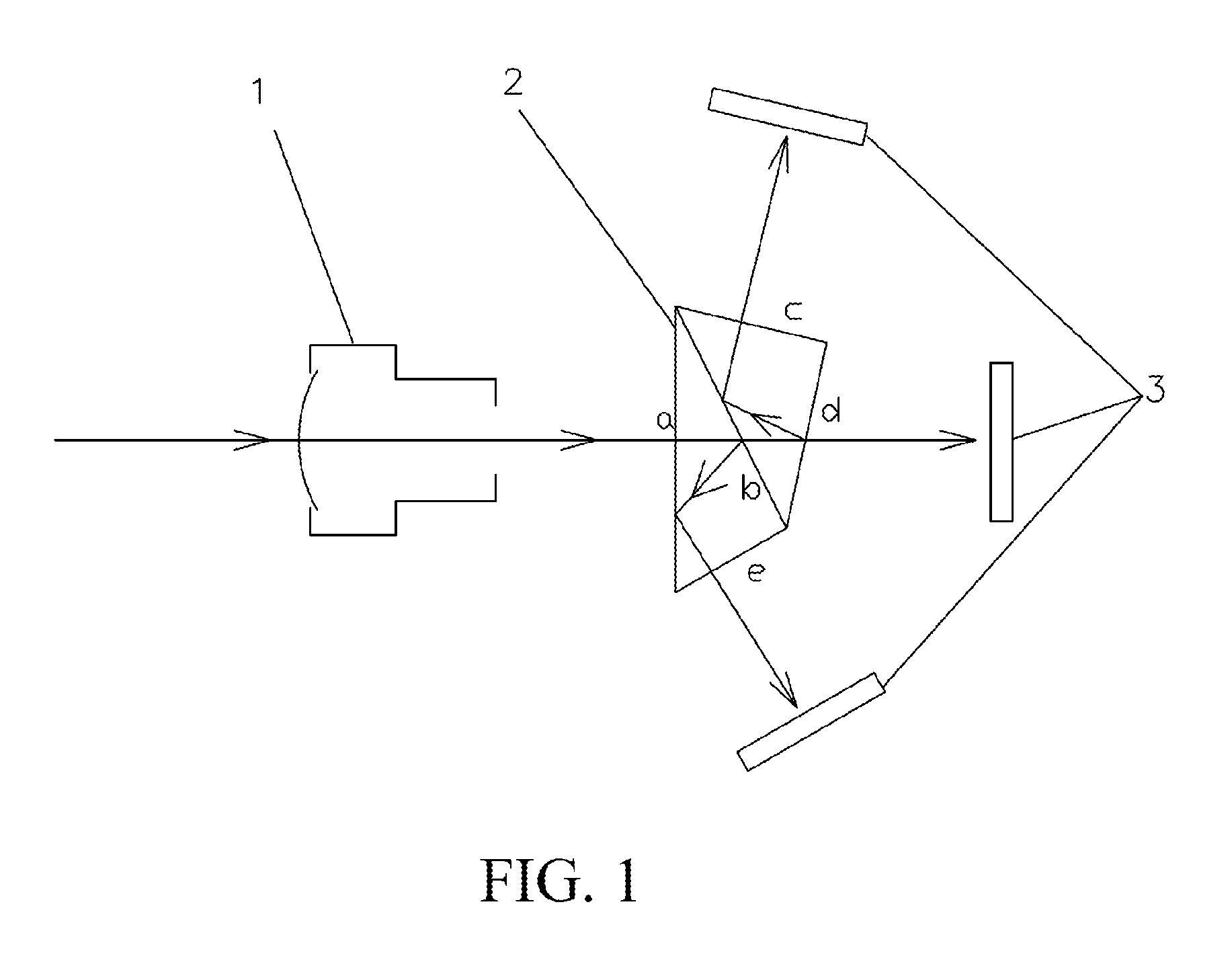
As shown in FIG. 1 and FIG. 2, an imaging system includes an optical lens 1, where a spectroscopical module 2 that can split a light wave transmitted from the optical lens 1 into three light waves in different wavelength ranges is disposed on an imaging side of the optical lens 1; and the imaging system further includes three photosensitive chips 3 configured to receive corresponding light waves, where the three photosensitive chips 3 are correspondingly distributed at three light waves emitted by the spectroscopical module 2, and the spectroscopical module 2 is a prism. The spectroscopical module may be a multifaceted prism structure, or may be a combination of prism structures. This is not specifically limited herein.
The spectroscopical module can implement transmission or reflection of light in a different-band spectrum. Incident light may be divided into three light beams with different bands, and the optical wavelength range mainly corresponds to light of three primary colors RGB for imaging and near infrared light.
A wavelength range of a light beam is 600 nm to 680 nm and 820 nm to 880 nm, and the light beam is mainly red light and near infrared light.
A wavelength range of a light beam is 500 nm to 580 nm and 820 nm to 880 nm, and the light beam is mainly green light and near infrared light.
A wavelength range of a light beam is 400 nm to 480 nm and 820 nm to 880 nm, and the light beam is mainly blue light and near infrared light.
As shown in FIG. 1 and FIG. 2, in this embodiment, the imaging system further includes an image processing module that can integrate and output light waves received by the photosensitive chips 3.
As shown in FIG. 1, incident light is focused by an optical lens, a spectroscopical module is a component prism, emergent light passes through a face a of the component prism and is projected to a face b. A reflected light beam, mainly blue light and near infrared light, is reflected by the face b and the face a, penetrates a face e, and then forms an image on a photosensitive chip. The projected light passes through the face b, is projected to a face d, and then a light beam, mainly green light and near infrared light, penetrates the face d and forms an image on a photosensitive chip. A light beam, mainly red light and near infrared light, is reflected by the face d and the face b, penetrates a face c, and then forms an image on a photosensitive chip. The three photosensitive chips separately receive light waves in particular wavelength ranges, and finally the image processing module implements restoration and reproduction of an image, thereby increasing definition of an optical system, enhancing color restoration, and implementing that an imaging system can form a clear image in environments with different illuminancy.
As shown in FIG. 1 and FIG. 2, in this embodiment, the spectroscopical module 2 includes a first spectroscopical component 21 and a second spectroscopical component 22. The first spectroscopical component 21 divides a light wave transmitted by the optical lens 1 into two light waves. One light wave is transmitted to the photosensitive chip 3, and the other light wave enters the second spectroscopical component 22. The second spectroscopical component 22 divides a light wave transmitted by the first spectroscopical component 21 into two light waves, and then separately transmits the two light waves to corresponding photosensitive chips 3. Finally, three light waves in different wavelength ranges are formed, and transmitted to corresponding photosensitive chips.
As shown in FIG. 1 and FIG. 2, in this embodiment, the photosensitive chip 3 corresponding to the light wave emitted by the first spectroscopical component 21 is disposed on one side of the first spectroscopical component 21, and the two photosensitive chips 3 corresponding to the two light waves emitted by the second spectroscopical component 22 are disposed on two sides of the second spectroscopical component 22.
As shown in FIG. 2, incident light is focused by an optical lens, and after emergent light passes through a face A on the first spectroscopical component and is projected to a face B, a transmission light beam, mainly red light and near infrared light, penetrates the face B, passes through a face C, and forms an image on a photosensitive chip. Reflected light is reflected by the face B, penetrates a face D, passes through a face E of the second spectroscopical component, and is projected to a face F. A light beam, mainly green light and near infrared light, is reflected by the face F, penetrates a face G, and forms an image on a photosensitive chip. A light beam, mainly blue light and near infrared light, penetrates the face F, passes through a face H, and forms an image on a photosensitive chip. The three photosensitive chips separately receive light waves in particular wavelength ranges, and finally the image processing module implements restoration and reproduction of an image, thereby increasing definition of an optical system, enhancing color restoration, and implementing that an imaging system can form a clear image in environments with different illuminancy.
As shown in FIG. 1 and FIG. 2, in this embodiment, the optical lens 1 is a fixed-focus optical lens, or may be a varifocal optical lens. This is not specifically limited herein.
* * * * *
D00000
D00001
D00002
XML
uspto.report is an independent third-party trademark research tool that is not affiliated, endorsed, or sponsored by the United States Patent and Trademark Office (USPTO) or any other governmental organization. The information provided by uspto.report is based on publicly available data at the time of writing and is intended for informational purposes only.
While we strive to provide accurate and up-to-date information, we do not guarantee the accuracy, completeness, reliability, or suitability of the information displayed on this site. The use of this site is at your own risk. Any reliance you place on such information is therefore strictly at your own risk.
All official trademark data, including owner information, should be verified by visiting the official USPTO website at www.uspto.gov. This site is not intended to replace professional legal advice and should not be used as a substitute for consulting with a legal professional who is knowledgeable about trademark law.