Switching and stability control for perpendicular magnetic tunnel junction device
Schabes , et al.
U.S. patent number 10,236,439 [Application Number 15/859,374] was granted by the patent office on 2019-03-19 for switching and stability control for perpendicular magnetic tunnel junction device. This patent grant is currently assigned to Spin Memory, Inc.. The grantee listed for this patent is Spin Memory, Inc.. Invention is credited to Bartlomiej Adam Kardasz, Mustafa Michael Pinarbasi, Manfred Ernst Schabes.


| United States Patent | 10,236,439 |
| Schabes , et al. | March 19, 2019 |
Switching and stability control for perpendicular magnetic tunnel junction device
Abstract
A magnetoresistive random-access memory (MRAM) is disclosed. The MRAM device includes a perpendicular magnetic tunnel junction device having a reference layer, a free layer, and a precessional spin current magnetic layer. The precessional spin current magnetic layer has a diameter that is different from a diameter of the free layer. The device is designed to provide control over the injection of stray fields and the electronic coupling between the precessional spin current magnetic layer and the free layer. Switching speed, switching current, and thermal barrier height for the device can be adjusted.
| Inventors: | Schabes; Manfred Ernst (Saratoga, CA), Pinarbasi; Mustafa Michael (Morgan Hill, CA), Kardasz; Bartlomiej Adam (Pleasanton, CA) | ||||||||||
|---|---|---|---|---|---|---|---|---|---|---|---|
| Applicant: |
|
||||||||||
| Assignee: | Spin Memory, Inc. (Fremont,
CA) |
||||||||||
| Family ID: | 65722166 | ||||||||||
| Appl. No.: | 15/859,374 | ||||||||||
| Filed: | December 30, 2017 |
| Current U.S. Class: | 1/1 |
| Current CPC Class: | H01F 10/3254 (20130101); H01L 43/10 (20130101); H01L 43/12 (20130101); H01L 43/08 (20130101); H01F 10/3272 (20130101); H01F 41/307 (20130101); H01F 10/3286 (20130101); H01L 43/02 (20130101); H01F 10/329 (20130101) |
| Current International Class: | H01L 43/10 (20060101); H01L 43/02 (20060101); H01F 10/32 (20060101); H01L 43/12 (20060101); H01L 43/08 (20060101) |
References Cited [Referenced By]
U.S. Patent Documents
| 341801 | May 1886 | Fox |
| 5541868 | July 1996 | Prinz |
| 5629549 | May 1997 | Johnson |
| 5640343 | June 1997 | Gallagher et al. |
| 5654566 | August 1997 | Johnson |
| 5691936 | November 1997 | Sakakima et al. |
| 5695846 | December 1997 | Lange et al. |
| 5695864 | December 1997 | Slonczewski |
| 5732016 | March 1998 | Chen et al. |
| 5856897 | January 1999 | Mauri |
| 5896252 | April 1999 | Kanai |
| 5966323 | October 1999 | Chen et al. |
| 6016269 | January 2000 | Peterson et al. |
| 6055179 | April 2000 | Koganei et al. |
| 6097579 | August 2000 | Gill |
| 6124711 | September 2000 | Tanaka et al. |
| 6134138 | October 2000 | Lu et al. |
| 6140838 | October 2000 | Johnson |
| 6154349 | November 2000 | Kanai et al. |
| 6172902 | January 2001 | Wegrowe et al. |
| 6233172 | May 2001 | Chen et al. |
| 6243288 | June 2001 | Ishikawa et al. |
| 6252798 | June 2001 | Satoh et al. |
| 6256223 | July 2001 | Sun |
| 6292389 | September 2001 | Chen et al. |
| 6347049 | February 2002 | Childress et al. |
| 6376260 | April 2002 | Chen et al. |
| 6385082 | May 2002 | Abraham et al. |
| 6436526 | August 2002 | Odagawa et al. |
| 6458603 | October 2002 | Kersch et al. |
| 6493197 | December 2002 | Ito et al. |
| 6522137 | February 2003 | Sun et al. |
| 6532164 | March 2003 | Redon et al. |
| 6538918 | March 2003 | Swanson et al. |
| 6545906 | April 2003 | Savtchenko et al. |
| 6563681 | May 2003 | Sasaki et al. |
| 6566246 | May 2003 | deFelipe et al. |
| 6603677 | August 2003 | Redon et al. |
| 6653153 | November 2003 | Doan et al. |
| 6654278 | November 2003 | Engel et al. |
| 6677165 | January 2004 | Lu et al. |
| 6710984 | March 2004 | Yuasa et al. |
| 6713195 | March 2004 | Wang et al. |
| 6714444 | March 2004 | Huai et al. |
| 6744086 | June 2004 | Daughton et al. |
| 6750491 | June 2004 | Sharma et al. |
| 6765824 | July 2004 | Kishi et al. |
| 6772036 | August 2004 | Eryurek et al. |
| 6773515 | August 2004 | Li et al. |
| 6777730 | August 2004 | Daughton et al. |
| 6785159 | August 2004 | Tuttle |
| 6812437 | November 2004 | Levy et al. |
| 6829161 | December 2004 | Huai et al. |
| 6835423 | December 2004 | Chen et al. |
| 6838740 | January 2005 | Huai et al. |
| 6842317 | January 2005 | Sugita et al. |
| 6847547 | January 2005 | Albert et al. |
| 6887719 | May 2005 | Lu et al. |
| 6888742 | May 2005 | Nguyen et al. |
| 6902807 | June 2005 | Argoitia et al. |
| 6906369 | June 2005 | Ross et al. |
| 6920063 | July 2005 | Huai et al. |
| 6933155 | August 2005 | Albert et al. |
| 6958927 | October 2005 | Nguyen et al. |
| 6967863 | November 2005 | Huai |
| 6980469 | December 2005 | Kent et al. |
| 6985385 | January 2006 | Nguyen et al. |
| 6992359 | January 2006 | Nguyen et al. |
| 6995962 | February 2006 | Saito et al. |
| 7002839 | February 2006 | Kawabata et al. |
| 7005958 | February 2006 | Wan |
| 7006375 | February 2006 | Covington |
| 7009877 | March 2006 | Huai et al. |
| 7041598 | May 2006 | Sharma |
| 7045368 | May 2006 | Hong et al. |
| 7149106 | December 2006 | Mancoff et al. |
| 7170778 | January 2007 | Kent et al. |
| 7190611 | March 2007 | Nguyen et al. |
| 7203129 | April 2007 | Lin et al. |
| 7227773 | June 2007 | Nguyen et al. |
| 7262941 | August 2007 | Li et al. |
| 7307876 | December 2007 | Kent et al. |
| 7324387 | January 2008 | Bergemont et al. |
| 7335960 | February 2008 | Han et al. |
| 7351594 | April 2008 | Bae et al. |
| 7352021 | April 2008 | Bae et al. |
| 7376006 | May 2008 | Bednorz et al. |
| 7378699 | May 2008 | Chan et al. |
| 7449345 | November 2008 | Horng et al. |
| 7476919 | January 2009 | Hong et al. |
| 7502249 | March 2009 | Ding |
| 7573737 | August 2009 | Kent et al. |
| 7598555 | October 2009 | Papworth-Parkin |
| 7619431 | November 2009 | DeWilde et al. |
| 7630232 | December 2009 | Guo |
| 7643332 | January 2010 | Leuschner |
| 7679155 | March 2010 | Korenivski |
| 7869265 | January 2011 | Shimizu |
| 7911832 | March 2011 | Kent et al. |
| 7936595 | May 2011 | Han et al. |
| 7986544 | July 2011 | Kent et al. |
| 8014193 | September 2011 | Nakayama et al. |
| 8279663 | October 2012 | Nakayama et al. |
| 8279666 | October 2012 | Dieny et al. |
| 8334213 | December 2012 | Mao |
| 8357982 | January 2013 | Kajiyama |
| 8363465 | January 2013 | Kent et al. |
| 8456883 | June 2013 | Liu |
| 8488375 | July 2013 | Saida et al. |
| 8492881 | July 2013 | Kuroiwa et al. |
| 8508979 | August 2013 | Saida et al. |
| 8535952 | September 2013 | Ranjan et al. |
| 8574928 | November 2013 | Satoh et al. |
| 8576616 | November 2013 | Saida et al. |
| 8582355 | November 2013 | Saida et al. |
| 8617408 | December 2013 | Balamane |
| 8716817 | May 2014 | Saida et al. |
| 8737122 | May 2014 | Saida et al. |
| 8737137 | May 2014 | Choy et al. |
| 8779537 | July 2014 | Huai |
| 8823118 | September 2014 | Horng |
| 8852760 | October 2014 | Wang et al. |
| 8860156 | October 2014 | Beach |
| 8878317 | November 2014 | Daibou et al. |
| 9019754 | April 2015 | Bedeschi |
| 9025368 | May 2015 | Saida et al. |
| 9082888 | July 2015 | Kent et al. |
| 9117995 | August 2015 | Daibou et al. |
| 9159342 | October 2015 | Kudo et al. |
| 9245608 | January 2016 | Chen et al. |
| 9263667 | February 2016 | Pinarbasi |
| 9299918 | March 2016 | Daibou et al. |
| 9337412 | March 2016 | Pinarbasi et al. |
| 9362486 | June 2016 | Kim et al. |
| 9378817 | June 2016 | Lee et al. |
| 9379314 | June 2016 | Park |
| 9406876 | August 2016 | Pinarbasi |
| 9472282 | October 2016 | Lee et al. |
| 9472748 | October 2016 | Kuo et al. |
| 9484527 | November 2016 | Han et al. |
| 9548445 | January 2017 | Lee et al. |
| 9589616 | March 2017 | Meng et al. |
| 9728712 | August 2017 | Kardasz et al. |
| 9741926 | August 2017 | Pinarbasi et al. |
| 9773540 | September 2017 | Zang et al. |
| 9773974 | September 2017 | Pinarbasi et al. |
| 9853206 | December 2017 | Pinarbasi |
| 10026892 | July 2018 | Pinarbasi et al. |
| 10032978 | July 2018 | Schabes et al. |
| 2002/0090533 | July 2002 | Zhang et al. |
| 2002/0105823 | August 2002 | Redon et al. |
| 2002/0132140 | September 2002 | Igarashi et al. |
| 2003/0117840 | June 2003 | Sharma et al. |
| 2003/0151944 | August 2003 | Saito |
| 2003/0197984 | October 2003 | Inomata et al. |
| 2003/0218903 | November 2003 | Luo |
| 2004/0012994 | January 2004 | Slaughter et al. |
| 2004/0061154 | April 2004 | Huai et al. |
| 2004/0094785 | May 2004 | Zhu et al. |
| 2004/0130936 | July 2004 | Nguyen et al. |
| 2004/0257717 | December 2004 | Sharma et al. |
| 2005/0041342 | February 2005 | Huai et al. |
| 2005/0051820 | March 2005 | Stojakovic et al. |
| 2005/0063222 | March 2005 | Huai et al. |
| 2005/0104101 | May 2005 | Sun et al. |
| 2005/0128842 | June 2005 | Wei |
| 2005/0136600 | June 2005 | Huai |
| 2005/0158881 | July 2005 | Sharma |
| 2005/0174702 | August 2005 | Gill |
| 2005/0180202 | August 2005 | Huai et al. |
| 2005/0184839 | August 2005 | Nguyen et al. |
| 2005/0201023 | September 2005 | Huai et al. |
| 2005/0237787 | October 2005 | Huai et al. |
| 2005/0280058 | December 2005 | Pakala et al. |
| 2006/0018057 | January 2006 | Huai |
| 2006/0049472 | March 2006 | Diao et al. |
| 2006/0087880 | April 2006 | Mancoff et al. |
| 2006/0092696 | May 2006 | Bessho |
| 2006/0132990 | June 2006 | Morise et al. |
| 2006/0227465 | October 2006 | Inokuchi et al. |
| 2007/0019337 | January 2007 | Apalkov et al. |
| 2007/0096229 | May 2007 | Yoshikawa et al. |
| 2007/0242501 | October 2007 | Hung et al. |
| 2007/0259209 | November 2007 | Slavin |
| 2008/0031035 | February 2008 | Rodmacq et al. |
| 2008/0049488 | February 2008 | Rizzo |
| 2008/0112094 | May 2008 | Kent et al. |
| 2008/0151442 | June 2008 | Mauri et al. |
| 2008/0151614 | June 2008 | Guo |
| 2008/0179699 | July 2008 | Horng |
| 2008/0259508 | October 2008 | Kent et al. |
| 2008/0291720 | November 2008 | Wang |
| 2008/0297292 | December 2008 | Viala et al. |
| 2009/0046501 | February 2009 | Ranjan et al. |
| 2009/0072185 | March 2009 | Raksha et al. |
| 2009/0091037 | April 2009 | Assefa et al. |
| 2009/0098413 | April 2009 | Kanegae |
| 2009/0161421 | June 2009 | Cho et al. |
| 2009/0209050 | August 2009 | Wang et al. |
| 2009/0209102 | August 2009 | Zhong et al. |
| 2009/0231909 | September 2009 | Dieny et al. |
| 2010/0019333 | January 2010 | Zhao et al. |
| 2010/0124091 | May 2010 | Cowburn |
| 2010/0193891 | August 2010 | Wang et al. |
| 2010/0232206 | September 2010 | Li |
| 2010/0246254 | September 2010 | Prejbeanu et al. |
| 2010/0271870 | October 2010 | Zheng et al. |
| 2010/0290275 | November 2010 | Park et al. |
| 2011/0001108 | January 2011 | Greene et al. |
| 2011/0032645 | February 2011 | Noel et al. |
| 2011/0058412 | March 2011 | Zheng et al. |
| 2011/0089511 | April 2011 | Keshtbod et al. |
| 2011/0121417 | May 2011 | Li |
| 2011/0133298 | June 2011 | Chen et al. |
| 2011/0216436 | September 2011 | Igarashi |
| 2012/0052258 | March 2012 | Op DeBeeck et al. |
| 2012/0069649 | March 2012 | Ranjan et al. |
| 2012/0120520 | May 2012 | Childress et al. |
| 2012/0155156 | June 2012 | Watts |
| 2012/0156390 | June 2012 | Araki |
| 2012/0181642 | July 2012 | Prejbeanu et al. |
| 2012/0188818 | July 2012 | Ranjan et al. |
| 2012/0228728 | September 2012 | Ueki et al. |
| 2012/0280336 | November 2012 | Jan |
| 2012/0280339 | November 2012 | Zhang et al. |
| 2012/0294078 | November 2012 | Kent et al. |
| 2012/0299133 | November 2012 | Son et al. |
| 2013/0001506 | January 2013 | Sato et al. |
| 2013/0001652 | January 2013 | Yoshikawa et al. |
| 2013/0021841 | January 2013 | Zhou et al. |
| 2013/0062714 | March 2013 | Zhu |
| 2013/0075845 | March 2013 | Chen et al. |
| 2013/0119495 | May 2013 | Vetro et al. |
| 2013/0157385 | June 2013 | Jung et al. |
| 2013/0244344 | September 2013 | Malmhall et al. |
| 2013/0267042 | October 2013 | Satoh et al. |
| 2013/0270523 | October 2013 | Wang et al. |
| 2013/0270661 | October 2013 | Yi et al. |
| 2013/0307097 | November 2013 | Yi et al. |
| 2013/0341801 | December 2013 | Satoh et al. |
| 2014/0009994 | January 2014 | Parkin et al. |
| 2014/0036573 | February 2014 | Ishihara et al. |
| 2014/0042571 | February 2014 | Gan et al. |
| 2014/0048896 | February 2014 | Huang et al. |
| 2014/0070341 | March 2014 | Beach et al. |
| 2014/0087483 | March 2014 | Ohsawa |
| 2014/0093701 | April 2014 | Sahoo et al. |
| 2014/0103472 | April 2014 | Kent et al. |
| 2014/0169085 | June 2014 | Wang et al. |
| 2014/0177316 | June 2014 | Otsuka et al. |
| 2014/0217531 | August 2014 | Jan |
| 2014/0252439 | September 2014 | Guo |
| 2014/0252519 | September 2014 | Kim |
| 2014/0264671 | September 2014 | Chepulskyy et al. |
| 2015/0008550 | January 2015 | Min et al. |
| 2015/0056368 | February 2015 | Wang et al. |
| 2015/0171316 | June 2015 | Park et al. |
| 2015/0279904 | October 2015 | Pinarbasi |
| 2015/0287910 | October 2015 | Lu |
| 2015/0357015 | December 2015 | Kent et al. |
| 2016/0027999 | January 2016 | Pinarbasi |
| 2016/0079518 | March 2016 | Pi |
| 2016/0087193 | March 2016 | Pinarbasi et al. |
| 2016/0093798 | March 2016 | Kim et al. |
| 2016/0099405 | April 2016 | Zimmer et al. |
| 2016/0111634 | April 2016 | Lee et al. |
| 2016/0126452 | May 2016 | Kuo et al. |
| 2016/0126453 | May 2016 | Chen et al. |
| 2016/0163965 | June 2016 | Han et al. |
| 2016/0163973 | June 2016 | Pinarbasi |
| 2016/0181508 | June 2016 | Lee et al. |
| 2016/0218278 | July 2016 | Pinarbasi et al. |
| 2016/0276006 | September 2016 | Ralph et al. |
| 2016/0284762 | September 2016 | Wang et al. |
| 2016/0315118 | October 2016 | Kardasz et al. |
| 2016/0315259 | October 2016 | Fennimore et al. |
| 2016/0372656 | December 2016 | Pinarbasi et al. |
| 2017/0025472 | January 2017 | Kim et al. |
| 2017/0033156 | February 2017 | Gan et al. |
| 2017/0033283 | February 2017 | Pinarbasi et al. |
| 2017/0033742 | February 2017 | Akerman |
| 2017/0047107 | February 2017 | Berger et al. |
| 2017/0084826 | March 2017 | Zhou et al. |
| 2017/0222132 | August 2017 | Pinarbasi et al. |
| 2017/0324029 | November 2017 | Pinarbasi et al. |
| 2017/0331032 | November 2017 | Chen et al. |
| 2017/0331033 | November 2017 | Kardasz et al. |
| 2017/0346002 | November 2017 | Pinarbasi et al. |
| 2018/0047894 | February 2018 | Pinarbasi et al. |
| 2018/0076382 | March 2018 | Park et al. |
| 2018/0114898 | April 2018 | Lee |
| 2018/0248110 | August 2018 | Kardasz et al. |
| 2018/0248113 | August 2018 | Pinarbasi et al. |
| 2766141 | Jan 2011 | CA | |||
| 105706259 | Jun 2006 | CN | |||
| 101036195 | Sep 2008 | CN | |||
| 102334207 | Jan 2012 | CN | |||
| 102959693 | Mar 2013 | CN | |||
| 105917480 | Aug 2016 | CN | |||
| 106062979 | Oct 2016 | CN | |||
| 107750382 | Mar 2018 | CN | |||
| 107851712 | Mar 2018 | CN | |||
| 1345277 | Sep 2003 | EP | |||
| 3298636 | Mar 2018 | EP | |||
| 2817998 | Jun 2002 | FR | |||
| 2832542 | May 2003 | FR | |||
| 2910716 | Jun 2008 | FR | |||
| H10-004012 | Jan 1998 | JP | |||
| H11-120758 | Apr 1999 | JP | |||
| H11-352867 | Dec 1999 | JP | |||
| 2001-195878 | Jul 2001 | JP | |||
| 2002-261352 | Sep 2002 | JP | |||
| 2002-357489 | Dec 2002 | JP | |||
| 2003-318461 | Nov 2003 | JP | |||
| 2005-044848 | Feb 2005 | JP | |||
| 2005-150482 | Jun 2005 | JP | |||
| 2005-535111 | Nov 2005 | JP | |||
| 4066477 | Mar 2006 | JP | |||
| 2006-128579 | May 2006 | JP | |||
| 2008-524830 | Jul 2008 | JP | |||
| 2009-027177 | Feb 2009 | JP | |||
| 2013-012546 | Jan 2013 | JP | |||
| 2014-039061 | Feb 2014 | JP | |||
| 5635666 | Dec 2014 | JP | |||
| 2015-002352 | Jan 2015 | JP | |||
| 2017-510989 | Apr 2017 | JP | |||
| 2017-527097 | Sep 2017 | JP | |||
| 2017-532752 | Dec 2017 | JP | |||
| 10-2014-0115246 | Sep 2014 | KR | |||
| 10-2015-0016162 | Feb 2015 | KR | |||
| WO 2009-080636 | Jul 2009 | WO | |||
| WO 2011-005484 | Jan 2011 | WO | |||
| WO 2014-062681 | Apr 2014 | WO | |||
| WO-2015-153142 | Oct 2015 | WO | |||
| 2016011435 | Jan 2016 | WO | |||
| WO-2016-014326 | Jan 2016 | WO | |||
| WO-2016-048603 | Mar 2016 | WO | |||
| WO-2016-171800 | Oct 2016 | WO | |||
| WO-2016-171920 | Oct 2016 | WO | |||
| WO-2016-204835 | Dec 2016 | WO | |||
| WO-2017-019134 | Feb 2017 | WO | |||
| WO-2017-030647 | Feb 2017 | WO | |||
| WO-2017-131894 | Aug 2017 | WO | |||
Other References
|
RH. Koch, et al., "Thermally Assisted Magnetization Reversal in Submicron-Sized Magnetic Thin Films"; Physical Review Letters; The American Physical Society; vol. 84, No. 23; Jun. 5, 2000, pp. 5419-5422 (4 pages). cited by applicant . K.J. Lee, et al., "Analytical investigation of spin-transfer dynamics using a perpendicular-to-plane polarizer"; Applied Physics Letters; American Institute of Physics; vol. 86, (2005); pp. 022505-1 to 022505-3 (3 pages). cited by applicant . Kirsten Martens, et al., "Thermally Induced Magnetic Switching in Thin Ferromagnetic Annuli"; NSF grants PHY-0351964 (DLS); 2005; 11 pages. cited by applicant . Kirsten Martens, et al., "Magnetic Reversal in Nanoscopic Ferromagnetic Rings"; NSF grants PHY-0351964 (DLS); 2006; 23 pages. cited by applicant . "Magnetic Technology Sprintronics, Media and Interface"; Data Storage Institute, R&D Highlights; Sep. 2010; 3 pages. cited by applicant . S. Ikeda, et al.; "A perpendicular-anisotropy CoFeB--MgO magnetic tunnel junction"; Nature Materials, vol. 9, Sep. 2010; pp. 721-724; 4 pages. cited by applicant . Soo-Man Seo, et al.; "Current-induced synchronized switching of magnetization;" Applied Physics Letters 101; 2012 American Institute of Physics; Aug. 7, 2012; 6 pages. cited by applicant . Kent, et al.; U.S. Appl. No. 61/715,111, filed Oct. 17, 2012, entitled "Inverted Orthogonal Spin Transfer Layer Stack". cited by applicant . Pinarbasi, et al.; U.S. Appl. No. 14/341,185, filed Jul. 25, 2014, entitled "Method for Manufacturing MTJ Memory Device". cited by applicant . Pinarbasi, et al.; U.S. Appl. No. 14/492,943, filed Sep. 22, 2014, entitled "Magnetic Tunnel Junction Structure for MRAM Device". cited by applicant . International Search Report and Written Opinion dated Jul. 10, 2015 in PCT/US2015/021580; 12 pages. cited by applicant . Pinarbasi, et al.; U.S. Appl. No. 14/814,036, filed Jul. 30, 2015, entitled "Precessional Spin Current Structure for MRAM". cited by applicant . Kardasz, et al.; U.S. Appl. No. 14/866,359, filed Sep. 25, 2015, entitled "Spin Transfer Torque Structure for MRAM Devices Having a Spin Current Injection Capping Layer". cited by applicant . International Search Report and Written Opinion dated Oct. 30, 2015 in PCT/US2015/040700; 11 pages. cited by applicant . International Search Report and Written Opinion dated Dec. 14, 2015 in PCT/US2015/047875; 13 pages. cited by applicant . Pinarbasi, et al.; U.S. Appl. No. 15/041,325, filed Feb. 11, 2016, entitled "Method for Manufacturing MTJ Memory Device". cited by applicant . Kardasz, et al.; U.S. Appl. No. 15/091,853, filed Apr. 6, 2016, entitled "High Annealing Temperature Perpendicular Magnetic Anisotropy Structure for Magnetic Random Access Memory". cited by applicant . Pinarbasi, et al.; U.S. Appl. No. 15/093,367, filed Apr. 7, 2016, entitled "Magnetic Tunnel Junction Structure for MRAM Device". cited by applicant . Pinarbasi, et al.; U.S. Appl. No. 15/097,576, filed Apr. 13, 2016, entitled "Polishing Stop Layer(s) for Processing Arrays of Semiconductor Elements". cited by applicant . Pinarbasi, et al.; U.S. Appl. No. 15/157,783, filed May 18, 2016, entitled "Memory Cell Having Magnetic Tunnel Junction and Thermal Stability Enhancement Layer". cited by applicant . Berger, et al.; U.S. Appl. No. 15/174,482, filed Jun. 6, 2016, entitled "Method and Apparatus for Bipolar Memory Write-Verify". cited by applicant . International Search Report and Written Opinion dated Jun. 17, 2016 in PCT/US2016/021324; 9 pages. cited by applicant . International Search Report and Written Opinion dated Jun. 17, 2016 in PCT/US2016/021691; 9 pages. cited by applicant . International Search Report and Written Opinion dated Jul. 15, 2016 in PCT/US2016/026473; 9 pages. cited by applicant . International Search Report and Written Opinion dated Jul. 21, 2016 in PCT/US2016/027445; 10 pages. cited by applicant . International Search Report and Written Opinion dated Sep. 26, 2016 in PCT/US2016/037843; 10 pages. cited by applicant . Pinarbasi, et al.; U.S. Appl. No. 15/445,260, filed Feb. 28, 2017, entitled "Precessional Spin Current Structure for MRAM". cited by applicant . Pinarbasi, et al.; U.S. Appl. No. 15/445,362, filed Feb. 28, 2017, entitled "Precessional Spin Current Structure for MRAM". cited by applicant . International Search Report and Written Opinion dated Apr. 7, 2017 in PCT/US2016/067444; 13 pages. cited by applicant . Notice of Allowance dated Apr. 21, 2017 in U.S. Appl. No. 15/157,783; 36 pages. cited by applicant . Pinarbasi, et al.; U.S. Appl. No. 15/656,398, filed Jul. 21, 2017, entitled "Memory Cell Having Magnetic Tunnel Junction and Thermal Stability Enhancement Layer". cited by applicant . Kardasz, et al.; U.S. Appl. No. 15/657,498, filed Jul. 24, 2017, entitled "Spin Transfer Torque Structure for MRAM Devices Having a Spin Current Injection Capping Layer". cited by applicant . Notice of Allowance dated Jul. 27, 2017 in U.S. Appl. No. 15/097,576; 22 pages. cited by applicant . Pinarbasi, et al.; U.S. Appl. No. 15/674,620, filed Aug. 11, 2017, entitled "Polishing Stop Layer(s) for Processing Arrays of Semiconductor Elements". cited by applicant . Schabes, et al.; U.S. Appl. No. 15/634,629, filed Jun. 27, 2017, entitled "MRAM with Reduced Stray Magnetic Fields". cited by applicant . Notice of Allowance dated Oct. 16, 2017 in U.S. Appl. No. 14/814,036; 16 pages. cited by applicant . Pinarbasi, et al.; U.S. Appl. No. 15/794,871, filed Oct. 26, 2017, entitled "Precessional Spin Current Structure for MRAM". cited by applicant . Tzoufras, et al.; U.S. Appl. No. 15/858,950, filed Dec. 29, 2017, entitled "AC Current Pre-Charge Write-Assist in Orthogonal STT-MRAM". cited by applicant . Gajek, et al.; U.S. Appl. No. 15/858,988, filed Dec. 29, 2017, entitled "Self-Generating AC Current Assist in Orthogonal STT MRAM". cited by applicant . Ryan, et al.; U.S. Appl. No. 15/859,015, filed Dec. 29, 2017, entitled "Shared Oscillator (STNO) for MRAM Array Write-Assist in Orthogonal STT-MRAM". cited by applicant . Tzoufras, et al.; U.S. Appl. No. 15/859,030, filed Dec. 29, 2017, entitled "AC Current Write-Assist in Orthogonal STT-MRAM". cited by applicant . Bozdag, et al.; U.S. Appl. No. 15/859,047, filed Dec. 29, 2017, entitled "Three-Terminal Mram with AC Write-Assist for Low Read Disturb". cited by applicant . Schabes, et al.; U.S. Appl. No. 15/862,788, filed Jan. 5, 2018, entitled "Perpendicular Magnetic Tunnel Junction Device with Skyrmionic Enhancement Layers for the Precessional Spin Current Magnetic Layer". cited by applicant . Schabes, et al.; U.S. Appl. No. 15/859,384, filed Dec. 30, 2017, entitled "Perpendicular Magnetic Tunnel Junction Device with Skyrmionic Assist Layers for Free Layer Switching". cited by applicant . Schabes, et al.; U.S. Appl. No. 15/859,381, filed Dec. 30, 2017, entitled "Perpendicular Magnetic Tunnel Junction Device with Precessional Spin Current Layer Having a Modulated Moment Density". cited by applicant . Schabes, et al.; U.S. Appl. No. 15/859,379, filed Dec. 30, 2017, entitled "Perpendicular Magnetic Tunnel Junction Device with Offset Precessional Spin Current Layer". cited by applicant . El Baraji, et al.; U.S. Appl. No. 15/859,514, filed Dec. 30, 2017, entitled "Microwave Write-Assist in Orthogonal STT-MRAM". cited by applicant . El Baraji, et al.; U.S. Appl. No. 15/859,517, filed Dec. 30, 2017, entitled "Microwave Write-Assist in Series-Interconnected Orthogonal STT-MRAM Devices". cited by applicant . Final Office Action dated Jul. 9, 2015 in U.S. Appl. No. 14/242,419; 19 pages. cited by applicant . Final Office Action dated Jun. 9, 2017 in U.S. Appl. No. 14/814,038; 19 pages. cited by applicant . Final Office Action dated Aug. 2, 2018 in U.S. Appl. No. 15/674,620. cited by applicant . NonFinal Office Action dated Dec. 9, 2017 in U.S. Appl. No. 14/866,359; 26 pages. cited by applicant . NonFinal Office Action dated Dec. 23, 2016 in U.S. Appl. No. 15/093,367; 13 pages. cited by applicant . NonFinal Office Action dated Jan. 25, 2017 in U.S. Appl. No. 15/097,576; 17 pages. cited by applicant . NonFinal Office Action dated Feb. 6, 2017 in U.S. Appl. No. 14/814,036; 22 pages. cited by applicant . NonFinal Office Action dated Jun. 29, 2018 in U.S. Appl. No. 15/859,381. cited by applicant . Nonfinal Office Action dated Jun. 26, 2018 in U.S. Appl. No. 15/859,384. cited by applicant . NonFinal Office Action dated Jun. 29, 2018 in U.S. Appl. No. 15/859,374. cited by applicant . Notice of Allowance dated Sep. 26, 2018 in U.S. Appl. No. 15/859,047; 10 pages. cited by applicant . Office Action dated Aug. 30, 2018 in Chinese Patent Application No. 201580009984.2. cited by applicant . International Search Report and Written Opinion dated May 10, 2018 in PCT/US2018/014645; 14 pages. cited by applicant . International Search Report and Written Opinion dated May 30, 2018 in PCT/US2018/014641; 13 pages. cited by applicant. |
Primary Examiner: Potter; Roy
Attorney, Agent or Firm: Arnold & Porter Kaye Scholer
Claims
What is claimed is:
1. A magnetic device, comprising: a first synthetic antiferromagnetic structure in a first plane having a magnetization vector that is perpendicular to the first plane and having a fixed magnetization direction; an antiferromagnetic coupling layer in a second plane and disposed above the first synthetic antiferromagnetic structure; a second synthetic antiferromagnetic structure in a third plane and disposed over the antiferromagnetic coupling layer; a magnetic reference layer in a fourth plane and disposed over the second synthetic antiferromagnetic structure, the magnetic reference layer having a magnetization vector that is perpendicular to the fourth plane and having a fixed magnetization direction; a non-magnetic tunnel barrier layer in a fifth plane and disposed over the magnetic reference layer; a free magnetic layer having a first diameter and disposed in a sixth plane over the non-magnetic tunnel barrier layer, the free magnetic layer having a magnetization vector that is perpendicular to the sixth plane and having a magnetization direction that can switch between a first magnetization direction to a second magnetization direction, the magnetic reference layer, the non-magnetic tunnel barrier layer and the free magnetic layer forming a magnetic tunnel junction; and a precessional spin current magnetic layer having a second diameter that is different from the first diameter, the precessional spin current magnetic layer disposed coaxially with the free magnetic layer in a seventh plane that is physically separated from the free magnetic layer and coupled to the free magnetic layer by a filter coupling layer that may induce ferromagnetic or antiferromagnetic coupling between the free magnetic layer and the filter layer.
2. The magnetic device of claim 1, wherein the second diameter is less than the first diameter.
3. The magnetic device of claim 1, wherein the second diameter is in the range of 5 nm to 100 nm.
4. The magnetic device of claim 1, wherein a ratio of the second diameter to the first diameter is in the range of 0.2 to 0.9.
5. The magnetic device of claim 1, wherein the precessional spin current magnetic layer is formed from Co.sub.xFe.sub.yB.sub.z, where y is in the range 40% to 70%, z is in the range 18% to 21%, and x+y+z=100%.
6. A magnetic device, comprising: a magnetic reference layer in a first plane, the magnetic reference layer having a magnetization vector that is perpendicular to the first plane and having a fixed magnetization direction; a non-magnetic tunnel barrier layer in a second plane and disposed over the magnetic reference layer; a free magnetic layer having a first diameter and disposed in a third plane over the non-magnetic tunnel barrier layer, the free magnetic layer having a magnetization vector that is perpendicular to the third plane and having a magnetization direction that can switch between a first magnetization direction to a second magnetization direction, the magnetic reference layer, the non-magnetic tunnel barrier layer and the free magnetic layer forming a magnetic tunnel junction; and a precessional spin current magnetic layer having a second diameter that is different from the first diameter, the precessional spin current magnetic layer disposed coaxially with the free magnetic layer in a fourth plane that is physically separated from the free magnetic layer and coupled to the free magnetic layer by a filter coupling layer that may induce ferromagnetic or antiferromagnetic coupling between the free magnetic layer and the filter layer.
7. The magnetic device of claim 6, wherein the second diameter is less than the first diameter.
8. The magnetic device of claim 6, wherein the second diameter is in the range of 5 nm to 100 nm.
9. The magnetic device of claim 6, wherein a ratio of the second diameter to the first diameter is in the range of 0.2 to 0.9.
10. The magnetic device of claim 6, wherein the precessional spin current magnetic layer is formed from Co.sub.xFe.sub.yB.sub.z, where y is in the range 40% to 70%, z is in the range 18% to 21%, and x+y+z=100%.
11. A method for manufacturing a magnetic device comprising the steps of: providing a magnetic tunnel junction including a magnetic reference layer, a non-magnetic tunnel barrier layer, and a free magnetic layer; depositing a filter coupling layer over the free magnetic layer; depositing a precessional spin current magnetic layer over the filter coupling layer; forming a partial pillar that includes the precessional spin current magnetic layer; depositing a hard mask layer over the precessional spin current magnetic layer; forming a pillar that includes the precessional spin current magnetic layer, the filter coupling layer, the free magnetic layer, the non-magnetic tunnel barrier layer, and the magnetic reference layer such that the precessional spin current magnetic layer has a diameter that is different from a diameter of the free magnetic layer; and depositing an electrical contact layer over the precessional spin current layer.
Description
CROSS-REFERENCE TO RELATED APPLICATIONS
Cross-reference is made to the following related applications, all of which are filed concurrently herewith, incorporated herein by reference, and assigned to assignee of this patent document: U.S. application Ser. No. 15/859,379, entitled "PERPENDICULAR MAGNETIC TUNNEL JUNCTION DEVICE WITH OFF ST PRECESSIONAL SPIN CURRENT LAYER," U.S. application Ser. No. 15/859,381, entitled "PERPENDICULAR MAGNETIC TUNNEL JUNCTION DEVICE WITH PRECESSIONAL SPIN CURRENT LAYER HAVING A MODULATED MOMENT DENSITY," U.S. application Ser. No. 15/862,788, entitled "PERPENDICULAR MAGNETIC TUNNEL JUNCTION DEVICE WITH SKYRMIONIC ENHANCEMENT LAYERS FOR THEPRECESSIONAL SPIN CURRENT MAGNETIC LAYER," and U.S. application Ser. No. 15/859,384, entitled "PERPENDICULAR MAGNETIC TUNNEL JUNCTION DEVICE WITH SKYRMIONIC ASSIST LAYERS FOR FREE LAYER SWITCHING."
FIELD
The present patent document relates generally to magnetic random access memory and, more particularly, to a magnetic tunnel junction stack having a precessional spin current layer that is designed to provide switching and stability control for the device.
BACKGROUND
Magnetoresistive random-access memory ("MRAM") is a non-volatile memory technology that stores data through magnetic storage elements. These elements are two ferromagnetic plates or electrodes that can hold magnetization and are separated by a non-magnetic material, such as a non-magnetic metal or insulator. In general, one of the plates has its magnetization pinned (i.e., a "reference layer"), meaning that this layer has a higher coercivity than the other layer and requires a larger magnetic field or spin-polarized current to change the orientation of its magnetization. The second plate is typically referred to as the free layer and its magnetization direction can be changed by a smaller magnetic field or spin-polarized current relative to the reference layer.
MRAM devices store information by changing the orientation of the magnetization of the free layer. In particular, based on whether the free layer is in a parallel or anti-parallel alignment relative to the reference layer, either a "1" or a "0" can be stored in each MRAM cell. Due to the spin-polarized electron tunneling effect, the electrical resistance of the cell changes due to the orientation of the magnetization of the two layers. The cell's resistance will be different for the parallel and anti-parallel states and thus the cell's resistance can be used to distinguish between a "1" and a "0." One important feature of MRAM devices is that they are non-volatile memory devices, since they maintain the information even when the power is off. The two plates can be sub-micron in lateral size and the magnetization direction can still be stable with respect to thermal fluctuations.
FIG. 1A illustrates a magnetic tunnel junction ("MTJ") 130 for a conventional MRAM device. The MTJ 130 includes reference layer 132, which is a magnetic layer, a non-magnetic tunneling barrier layer 134, which generally is an insulator at large layer thickness but at small layer thickness admits the flow of an appreciable quantum mechanical tunnel current, and a free layer 136, which is also a magnetic layer. The magnetization direction of the magnetic layers of the MTJ 130 can be in the planes of those layers or perpendicular to the planes of those layers. As shown in FIG. 1A, the magnetic reference layer 132 has a magnetization direction perpendicular to its plane. Also as seen in FIG. 1A, the free layer 136 also has a magnetization direction perpendicular to its plane, but its direction can vary by 180 degrees. Because the magnetization direction of the magnetic layers of the MTJ 130 is perpendicular to the planes of those layers, the MTJ 130 shown in FIG. 1A is known as a perpendicular MTJ ("pMTJ").
As shown in FIG. 1A, electrical contact layers 170, 172 can optionally be used to provide electrical contact to the MTJ 130. When the magnetization of the free layer 136 is oriented in a direction parallel to the magnetization direction of the reference layer 132, electrons will be more likely to tunnel across the tunneling barrier layer 134, and thus resistance across the MTJ 130 will be lower. Alternatively, when the magnetization of the free layer 136 is oriented in a direction that is anti-parallel to the magnetization direction of the reference layer 132, electrons will be less likely to tunnel across the tunneling barrier layer 134, making the resistance across the MTJ 130 significantly higher. It is these different resistances that can be used to distinguish and store a digital "1" or "0" bit.
The MTJ 130 may also form part of a larger MTJ stack 100, as shown in FIG. 1B, which may include a number of other optional layers that can be used to facilitate operation of the MTJ. As described in connection with FIG. 1A, the MTJ stack 100 of FIG. 1B may include electrical contact layers 170, 172 for providing electrical contact across the MTJ stack 100, including the MTJ 130. The MTJ 130 may be disposed above an antiferromagnetic layer or a synthetic antiferromagnetic ("SAF") structure 120, which may include multiple layers as shown in FIG. 1B. For example, as shown in FIG. 1B, the SAF structure 120 may include two or more thin magnetic layers, including a lower "SAF1" layer 122 and an upper "SAF2" layer 126 having opposite or anti-parallel magnetization directions separated by an antiferromagnetic coupling layer 124 or spacer layer that is not magnetic. The SAF structure 120 also may be formed over a seed layer 110, as shown in FIG. 1B, and over a substrate (not shown). Note that as used herein, terms such as "lower," "upper," "top," "bottom," and the like are provided for convenience in explaining the various embodiments, and are not limiting in any way.
Spin transfer torque or spin transfer switching, may be used in connection with an MTJ 130. In such a configuration, a filter layer 150 may be used to alter the spin of electrons passing through the MTJ 130. For example, the filter layer may be a polarizer layer designed to further align the spin of electrons (i.e., to further "polarize" the electrons) passing through the MTJ 130 beyond the alignment already provided by the reference layer 132. U.S. patent application Ser. No. 14/814,036, filed by Pinarbasi et al., and assigned to the assignee of this patent document describes using a polarizer layer. The disclosure of U.S. patent application Ser. No. 14/814,036 is incorporated herein by reference in its entirety. The spin-aligned or "polarized" electrons are used to change the magnetization orientation of the free layer 136 in the MTJ 130. In general, electrons possess a spin, a quantized number of angular momentum intrinsic to the electron. An electrical current is generally unpolarized, i.e., it consists of 50% spin up and 50% spin down electrons. Passing a current though a magnetic layer, like the filter layer 150 or the reference layer 132, polarizes electrons with the spin orientation corresponding to the magnetization direction of the magnetic layer, thus producing a spin-polarized current. If a spin-polarized current is passed to the magnetic region of a free layer 136 of the MTJ 130, the electrons will transfer a portion of their spin-angular momentum to the free layer to produce a torque on the magnetization of the free layer. Thus, this spin transfer torque can switch the magnetization of the free layer, and can be used to write either a "1" or a "0" based on whether the free layer 136 is in the parallel or anti-parallel states relative to the reference layer.
As shown in FIG. 1B, the filter layer 150 and a filter coupling layer 140 are disposed above the free layer 136 of the MTJ 130. The filter layer 150 is physically separated from the free layer 136 and is coupled to the free layer 136 by the coupling layer 140. The filter layer 150 can be used to polarize a current of electrons ("spin-aligned electrons") applied to MTJ structure 100 in the manner described above.
The filter layer 150 is a precessional spin current ("PSC") magnetic layer, an example of which is described in detail in U.S. patent application Ser. No. 14/814,036, filed by Pinarbasi et al., and assigned to the assignee of this patent document. Additionally, a precessional spin current structure for MRAIVI is described in U.S. patent application Ser. Nos. 15/445,260 and 15/445,362, both of which are filed by Pinarbasi et al. and are assigned to the assignee of this patent document. The disclosures of U.S. patent application Ser. Nos. 15/445,260 and 15/445,362 are both incorporated herein by reference in their entireties.
Switching speed, switching current, and thermal barrier height are all parameters that affect the overall performance of MRAM devices. In such devices, it is desirable to maximize switching speed while minimizing switching current and thermal barrier height. However, a selected value for one of those parameters may limit the possible values for others of those parameters. Thus, tradeoffs between selected values must be made in order to maintain optimal performance. In conventional pMTJ devices, the tradeoff between switching speed, switching current, and thermal barrier height, while important, has been difficult to optimize. Moreover, in conventional pMTJ devices, the filter layer (e.g., precessional spin current layer) has a size and shape that are the same as those of the free layer. For example, in conventional pMTJ devices, the filter layer has a diameter that is the same as a diameter of the free layer. Furthermore, in conventional pMTJ devices, the filter layer and the free layer are formed coaxially with one another. Also, in conventional pMTJ devices, the filter layer has a moment density that is uniform throughout the layer.
SUMMARY
An MRAM device is disclosed that has a precessional spin current layer with a size or a shape that is different from that of the free layer of the pMTJ. The precessional spin current layer may have a center that is offset relative to a center of the free layer, such that the precessional spin current layer and the free layer are not coaxial with one another. The ability to vary the size, shape, or offset of the precessional spin current layer with respect to that of the free layer provides additional degrees of freedom by which the injection of stray fields and the electronic coupling between the precessional spin current and the free layer can be controlled and optimized. Moreover, the off-center design may be used to adjust the location of the stray-field injection in the free layer.
Also disclosed is an MRAM device that has a precessional spin current layer in which a moment density is varied and non-uniform throughout the layer. For example, the moment density of the precessional spin current layer may vary radially over the diameter of the layer. As one example, the moment density at the center of the precessional spin current layer is greater than a moment density at a perimeter of the precessional spin current layer. The use of a precessional spin current layer with a non-uniform moment density provides an additional degree of freedom by which the injection of stray fields and the electronic coupling between the precessional spin current and the free layer can be controlled and optimized. Moreover, the decreased moment density at the perimeter of the precessional spin current layer helps to stabilize the free layer when the effective magnetic field (B.sub.eff) of the precessional spin current layer is high. In addition, spin accumulation can be increased near the center of the precessional spin current layer, helping to switch the free layer.
In an embodiment, a magnetic device may include a first synthetic antiferromagnetic structure in a first plane having a magnetization vector that is perpendicular to the first plane and having a fixed magnetization direction. An embodiment may also include an antiferromagnetic coupling layer in a second plane and disposed above the first synthetic antiferromagnetic structure and a second synthetic antiferromagnetic structure in a third plane and disposed over the antiferromagnetic coupling layer. An embodiment further includes a magnetic reference layer in a fourth plane and disposed over the second synthetic antiferromagnetic structure. The magnetic reference layer has a magnetization vector that is perpendicular to the fourth plane and has a fixed magnetization direction. (For the purposes of this patent document, angles within several degrees of perpendicular are within the scope of what is considered perpendicular.) An embodiment further includes a non-magnetic tunnel barrier layer in a fifth plane and disposed over the magnetic reference layer. An embodiment also includes a free magnetic layer disposed in a sixth plane over the non-magnetic tunnel barrier layer. The free magnetic layer has a magnetization vector that is perpendicular to the sixth plane and has a magnetization direction that can switch between a first magnetization direction to a second magnetization direction. The magnetic reference layer, the non-magnetic tunnel barrier layer and the free magnetic layer form a magnetic tunnel junction. An embodiment also includes a precessional spin current magnetic layer in a seventh plane that is physically separated from the free magnetic layer and coupled to the free magnetic layer by a filter coupling layer that may induce ferromagnetic or antiferromagnetic coupling between the free magnetic layer and the filter layer.
In an embodiment of the magnetic device, the precessional spin current magnetic layer has a diameter that is different from a diameter of the free layer.
In an embodiment of the magnetic device, the diameter of the precessional spin current magnetic layer is less than the diameter of the free layer.
In an embodiment of the magnetic device, the diameter of the precessional spin current magnetic layer is in the range of 5 nm to 100 nm.
In an embodiment of the magnetic device, a ratio of the diameter of the precessional spin current magnetic layer to the diameter of the free layer is in the range of 0.2 to 0.9.
In an embodiment of the magnetic device, the precessional spin current magnetic layer is formed from Co.sub.xFe.sub.yB.sub.z, where y is in the range 40% to 70%, z is in the range 18% to 21%, and x+y+z=100%.
BRIEF DESCRIPTION OF THE DRAWINGS
The accompanying drawings, which are included as part of the present specification, illustrate the presently preferred embodiments and, together with the general description given above and the detailed description given below, serve to explain and teach the principles of the MTJ devices described herein.
FIG. 1A illustrates a conventional MTJ capable of use in an MRAIVI device.
FIG. 1B illustrates a conventional MTJ stack for an MRAIVI device.
FIG. 2A illustrates an MTJ stack for an MRAM device with a precessional spin current layer having a diameter that is different from a diameter of the free layer.
FIG. 2B illustrates a precessional spin current layer of an MTJ stack for an MRAM device, the precessional spin current layer having a diameter that is different from a diameter of the free layer.
FIG. 3A illustrates an MTJ stack for an MRAM device with a precessional spin current layer having a central axis that is offset from a central axis of the free layer.
FIG. 3B illustrates a circular precessional spin current layer of an MTJ stack for an MRAM device, the precessional spin current layer having a central axis that is offset from a central axis of the free layer.
FIG. 3C illustrates a non-circular precessional spin current layer of an MTJ stack for an MRAM device, the precessional spin current layer having a central axis that is offset from a central axis of the free layer.
FIG. 4A illustrates an MTJ stack for an MRAM device with a precessional spin current layer having a non-uniform moment density.
FIG. 4B illustrates a precessional spin current layer of an MTJ stack for an MRAM device, the precessional spin current layer having a non-uniform moment density.
FIG. 5A illustrates an MTJ stack for an MRAM device with a precessional spin current layer having a sequence of regions with varying moment densities.
FIG. 5B illustrates a precessional spin current layer of an MTJ stack for an MRAM device, the precessional spin current layer having a sequence of regions with varying moment densities.
FIG. 6 illustrate flow charts showing manufacturing steps for an MRAM device in accordance with embodiments.
FIG. 7 illustrate flow charts showing manufacturing steps for an MRAM device in accordance with embodiments.
FIG. 8 illustrates a flow chart showing manufacturing steps for an MRAM device in accordance with embodiments.
The figures are not necessarily drawn to scale and the elements of similar structures or functions are generally represented by like reference numerals for illustrative purposes throughout the figures. The figures are only intended to facilitate the description of the various embodiments described herein; the figures do not describe every aspect of the teachings disclosed herein and do not limit the scope of the claims.
DETAILED DESCRIPTION
The following description is presented to enable any person skilled in the art to create and use a precessional spin current structure for a pMTJ device that provides switching and stability control for the device. Each of the features and teachings disclosed herein can be utilized separately or in conjunction with other features to implement the disclosed system and method. Representative examples utilizing many of these additional features and teachings, both separately and in combination, are described in further detail with reference to the attached drawings. This detailed description is merely intended to teach a person of skill in the art further details for practicing preferred aspects of the present teachings and is not intended to limit the scope of the claims. Therefore, combinations of features disclosed in the following detailed description may not be necessary to practice the teachings in the broadest sense, and are instead taught merely to describe particularly representative examples of the present teachings.
In the following description, for purposes of explanation only, specific nomenclature is set forth to provide a thorough understanding of the present teachings. However, it will be apparent to one skilled in the art that these specific details are not required to practice the present teachings.
This patent document discloses a precessional spin current structure for a pMTJ device that provides switching and stability control for the device. For example, by designing a precessional spin current structure in accordance with this patent document, additional control of the injection of stray fields and the electronic coupling between the precessional spin current layer and the pMTJ can be achieved. In addition, this patent document provides disclosures for how switching speed, switching current, and thermal barrier height can be adjusted in an MRAIVI device thereby providing advantages to commercial applications of said pMTJ devices.
According to embodiments, a precessional spin current layer may have a size that is different than that of a free layer. For example, a precessional spin current layer may have a diameter that is less than a diameter of the free layer. In some embodiments, a precessional spin current layer may be coaxial with a free layer. In other embodiments, a precessional spin layer may be offset (i.e., not coaxial) from the free layer. In some embodiments, a precessional spin current layer may have a shape that is the same as that of the free layer, and may have, for example, a circular shape. In other embodiments, a precessional spin current layer may have a shape that is not the same as that of the free layer, and may form, for example, a crescent shape. In some embodiments, a moment density of a precessional spin current layer may be uniform. In other embodiments, a moment density may be non-uniform and may vary throughout a precessional spin current layer. For example, a precessional spin current layer may have a moment density at its center that is greater than a moment density at its perimeter.
FIG. 2A shows an MTJ stack 200 that can be used as an MRAM device. The MTJ stack 200 includes an MTJ 230, which includes which includes a magnetic reference layer 232, a non-magnetic tunneling barrier layer 234, and a magnetic free layer 236. The magnetic reference layer 232 has a magnetization direction perpendicular to its plane, and the free layer 236 also has a magnetization direction perpendicular to its plane, but as shown in FIG. 2A, its direction can vary by 180 degrees. The differences in resistance based on whether the magnetization direction of the free layer 236 is parallel to or anti-parallel to the magnetization direction of the reference layer 232 can be used to distinguish and store a digital "1" or "0" bit. The non-magnetic tunneling barrier layer 234 may be formed from MgO, or other suitable material. In embodiments where MgO is used to form the tunneling barrier layer 234, that material may have a crystalline texture that is a (001) texture.
The MTJ stack 200 may also include a number of other optional layers that can be used to facilitate operation of the MTJ 230. For example, the MTJ stack 200 may include electrical contact layers 270, 272 for providing electrical contact across the MTJ stack 200. According to an embodiment, the electrical contact layers 270, 272 may be electrodes for providing a voltage across the MTJ stack 200, and may be formed from any suitable conducting material. The MTJ 230 also can be disposed above an SAF structure 220, which may include multiple sub-layers and structures as shown in FIG. 2A. For example, as shown in FIG. 2A, the SAF structure 220 may include two or more thin magnetic layers, such as a lower "SAF1" layer 222 and an upper "SAF2" layer 226, having opposite or anti-parallel magnetization directions separated by an antiferromagnetic coupling layer 224 (or "spacer" layer) that is not magnetic. The SAF structure 220 also may be formed over a seed layer 210 and over a substrate (not shown). In general, in each of the MTJ stacks described herein, the lower SAF1 layer of the MTJ can be formed on a seed layer, as shown in FIG. 2A and the other figures using similar numbering, and all layers can be formed on a substrate (not shown in the figures). Magnetic layers of the stack 200, such as reference layer 232, the free layer 236, and the magnetic SAF layers 222, 226, may be made from a variety of materials, including Co, Ni, Fe, or alloys of those elements. In addition, magnetic layers of the stack 200 may be made from alloys of magnetic elements with non-magnetic elements, such as B, Ta, W, Pt, and Pd. Additionally, magnetic layers of the stack 200 may also be made using multiple layers of magnetic elements or alloys and non-magnetic elements such as Pt and Pd, including, for example, CoPt or CoPd multi-layers. The antiferromagnetic coupling layer 224 may be made from materials such as Ru or Cr, or other materials suitable to induce anti-parallel alignment between the lower SAF1 layer 222 and the upper SAF2 layer 226.
The MTJ stack 200 includes a precessional spin current layer 250 for facilitating spin transfer torque switching between states. The precessional spin current layer enhances the alignment of the spin of electrons passing through the MTJ 230. The precessional spin current layer 250 and a filter coupling layer 240 are disposed above the free layer 236 of the MTJ 230. The precessional spin current layer 250 may be made from materials such as Co.sub.xFe.sub.yB.sub.z, which contains x-percent Co, y-percent Fe, and z-percent B, where y is in the range of 40% to 70%, z is in the range of 18% to 21%, and x+y+z=100%. For example, according to an embodiment, the filter layer 250 may be made from Co.sub.40Fe.sub.40B.sub.20. The filter coupling layer 240 can be made of MgO, Cr, Ta, TaN, or other suitable materials to permit it to align the spin of electrons passing through the MTJ 230.
The MTJ stack 200 may be designed to reduce stray magnetic fields generated by magnetic layers of the stack 200, thereby increasing the electrical and retention performance of the stack 200 by reducing switching asymmetry in the free layer 236 and by reducing asymmetry in the dynamic magnetic rotation of the precessional spin current layer 250. U.S. patent application Ser. No. 15/634,629, filed by Schabes et al., and assigned to the assignee of this patent document describes techniques for reducing stray magnetic fields, including techniques for depositing an SAF structure and for the use of one or more auxiliary exchange coupling layers in an MTJ stack. The disclosure of U.S. patent application Ser. No. 15/634,629 is incorporated herein by reference in its entirety.
The thickness of the layers of the MTJ stack 200 can vary, and can be adjusted to produce the appropriate or desired electrical performance. Examples of thickness that may be used in certain circumstances are provided. It will be understood by those skilled in the art that these numbers can be adjusted or scaled consistent with the principles described herein. By way of example, the reference layer 232 may have a thickness in the range of 0.5 nanometers ("nm") to 3.0 nm, the free layer 236 may have a thickness in the range of 0.6 nm to 3.0 nm, and the tunnel barrier layer 234 may have a thickness in the range of 0.3 nm to 1.5 nm. By way of example, the lower and upper SAF layers 222, 226 may have a thickness in the range of 1 nm to 15 nm, and the antiferromagnetic coupling layer 224 may have a thickness in the range of 0.5 nm to 1.2 nm. For example, according to embodiments, the SAF layers 222, 226 can have a thickness of 6 nm. The precessional spin current layer 250 may have a thickness in the range from 0.5 nm to 4.5 nm and the filter coupling layer 240 may have a thickness in the range from 0.2 nm to 1.5 nm.
Other dimensions of the layers of the MTJ stack 200 can also be adjusted, as appropriate, to improve electrical performance or to optimize physical characteristics of the MTJ stack 200. As shown in FIGS. 2A and 2B, the precessional spin current layer 250 may have a diameter that is different from a diameter of the free layer 236. For example, use of a precessional spin current layer 250 with a diameter that is less than a diameter of the free layer 360 allows for further control over the switching and stability of the MTJ 230. According to an embodiment, the free layer 236 has a diameter d.sub.FRL that is in the range of 5 nm to 100 nm (i.e., 5 nm.ltoreq.d.sub.FRL.ltoreq.100 nm). In that embodiment the precessional spin current layer 250 has a diameter d.sub.PSC that is selected such that the ratio of the diameter d.sub.PSC of the precessional spin current layer 250 to the diameter d.sub.FRL of the free layer 236 is in the range of 0.2 to 0.9, provided the diameter d.sub.PSC of the precessional spin current layer 250 is greater than a minimum diameter of 3 nm (i.e., 0.2.ltoreq.d.sub.PSC/d.sub.FRL.ltoreq.0.9, if d.sub.PSC>3 nm; otherwise d.sub.PSC=3 nm).
According to an embodiment, the precessional spin current layer 250 is provided such that it is coaxial with the free layer 236. As shown in FIGS. 2A and 2B, the precessional spin current layer 256 has a central axis A.sub.1 that is the same as a central axis A.sub.2 of the free layer 236.
FIG. 3A shows an MTJ stack 300 that can be used as an MRAM device. The MTJ stack 300 includes an MTJ 330, which includes a magnetic reference layer 332, a non-magnetic tunneling barrier layer 334, and a magnetic free layer 336. The MTJ stack 300 may also include an electrical contact layers 370, 372, an SAF structure 320, which may include a lower SAF1 layer 322, an upper SAF2 layer 326, and a nonmagnetic antiferromagnetic coupling layer 324 therebetween. The SAF structure 320 also may be formed over a seed layer 310 and over a substrate (not shown). The MTJ stack 300 further includes a precessional spin current layer 350 and a filter coupling layer 340 disposed above the free layer 336 of the MTJ 330. The layers shown in FIG. 3A may have dimensions and may be formed of materials in accordance with the dimensions and materials discussed above with respect to corresponding layers shown in FIG. 2A. Similarly, the purpose served by each layer shown in FIG. 3A is in accordance with the purposes discussed above with respect to each corresponding layer shown in FIG. 2A.
In the embodiment illustrated in FIGS. 3A, 3B, and 3C the precessional spin current layer 350 is provided such that it is axially offset from the free layer 336 by a distance dx. As shown in FIGS. 3A, 3B, and 3C the precessional spin current layer 350 has a central axis A.sub.3 that is different from a central axis A.sub.4 of the free layer 336. According to an embodiment, the ratio of the offset distance dx to a diameter d.sub.FRL of the free layer 336 is in the range of 0 to 0.4 (i.e., 0<dx/d.sub.FRL.ltoreq.0.4). The offset between the precessional spin current layer 350 and the free layer 336 provides an additional degree of freedom by which switching and stability of the MTJ 330 may be controlled. In addition, the offset design can be used to adjust the location of the stray-field injection in the free layer 336.
As illustrated in FIG. 3B, the precessional spin current layer 350 may have a circular shape. FIG. 3C illustrates an embodiment in which the precessional spin current layer 350 has a non-circular shape. In that embodiment, the profile of the precessional spin current layer 350 over the free layer 356 forms a crescent shape. Such a shape can be achieved, for example, by forming a precessional spin current layer 350 with a portion that overhangs the free layer 336 and etching away the overhanging portion during manufacture of the MTJ stack 300.
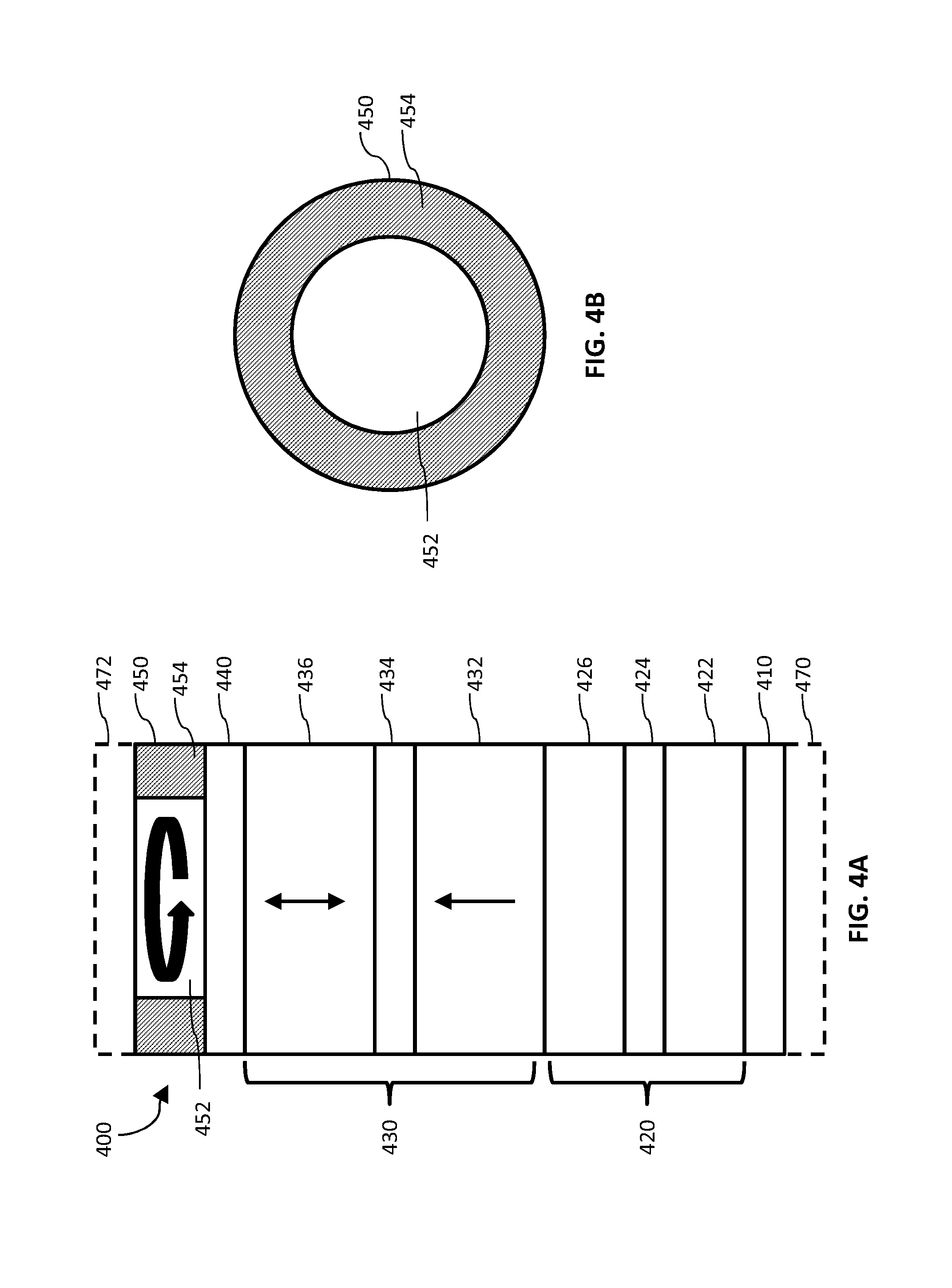
FIG. 4A shows an MTJ stack 400 that can be used as an MRAM device. The MTJ stack 400 includes an MTJ 430, which includes a magnetic reference layer 432, a non-magnetic tunneling barrier layer 434, and a magnetic free layer 436. The MTJ stack 400 may also include an electrical contact layers 470, 472, an SAF structure 420, which may include a lower SAF1 layer 422, an upper SAF2 layer 426, and a nonmagnetic antiferromagnetic coupling layer 424 therebetween. The SAF structure 420 also may be formed over a seed layer 410 and over a substrate (not shown). The MTJ stack 400 further includes a precessional spin current layer 450 and a filter coupling layer 440 are disposed above the free layer 436 of the MTJ 430. The layers shown in FIG. 4A may have dimensions and may be formed of materials in accordance with the dimensions and materials discussed above with respect to corresponding layers shown in FIGS. 2A and 3A. Similarly, the purpose served by each layer shown in FIG. 4A is in accordance with the purposes discussed above with respect to each of the corresponding layers shown in FIGS. 2A and 3A.
In the embodiment illustrated in FIGS. 4A and 4B, the precessional spin current layer 450 has a center with a moment density that is different from a moment density at a perimeter of the precessional spin current layer 450. For example, the precessional spin current layer may include a first region 452 having a high moment density and a second region 454 having a relatively low moment density. According to an embodiment, the materials for the first region 452 having the high moment density and the second region 454 having the low moment density are both alloys of the type Co.sub.xFe.sub.yB.sub.z, which contains x-percent Co, y-percent Fe, and z-percent B, where y is in the range of 40% to 70%, z is in the range of 18% to 21%, and x+y+z=100%. According to that embodiment, the percentage of Fe y.sub.HDR in the high moment density region 452 is relatively higher compared to the percentage of Fe y.sub.LDR in the low moment density region 454, and the ratio of the percentage of Fe y.sub.HDR in the high moment density region 452 to the percentage of Fe y.sub.LDR in the low moment density region 454 is in the range of 1.15 to 1.75 (i.e., 1.15.ltoreq.y.sub.HDR/y.sub.LDR.ltoreq.1.75). According to another embodiment, the material for the low moment density region 454 is an alloy of the type Co.sub.xFe.sub.yB.sub.z, which contains x-percent Co, y-percent Fe, and z-percent B, where y is in the range of 40% to 70%, z is in the range of 18% to 21%, and x+y+z=100%, and the material for the high moment density region 452 is Fe. According to another embodiment, the material for the high moment density region 452 is FeCo.
According to an embodiment, a distinct boundary may exist between the high moment density region 452 and the low moment density region 454. For example, the boundary between the high moment density region 452 and the low moment density region 454 may resemble a step function. According to another embodiment, a less distinct boundary may exist between the high moment density region 452 and the low moment density region 454. For example, the boundary between the high moment density region 452 and the low moment density region 454 may resemble a Gaussian, super-Gaussian, or other desirable function. In such embodiments, a high temperature diffusion process may be used to induce diffusive processes for smoothing out the chemical concentration profiles of the high moment density region 452 and the low moment density region 454.
Providing a precessional spin current layer 450 having a non-uniform moment density allows for further control over the switching and stability of the MTJ 430. In addition, the reduction of the moment density of the precessional spin current layer 450 at its perimeter helps stabilize the free layer 430 when the effective magnetic field of the precessional spin current layer 450 is high. Furthermore, spin accumulation can be increased near the center of the precessional spin current layer 450, helping to switch the free layer 436.
FIG. 5A shows an MTJ stack 500 that can be used as an MRAM device. The MTJ stack 500 includes an MTJ 530, which includes which includes a magnetic reference layer 532, a non-magnetic tunneling barrier layer 534, and a magnetic free layer 536. The MTJ stack 500 may also include an electrical contact layers 570, 572, an SAF structure 520, which may include a lower SAF1 layer 522, an upper SAF2 layer 526, and a nonmagnetic antiferromagnetic coupling layer 524 therebetween. The SAF structure 520 also may be formed over a seed layer 510 and over a substrate (not shown). The MTJ stack 500 further includes a precessional spin current layer 550 and a filter coupling layer 540 are disposed above the free layer 536 of the MTJ 530. The layers shown in FIG. 5A may have dimensions and may be formed of materials in accordance with the dimensions and materials discussed above with respect to corresponding layers shown in FIGS. 2A, 3A, and 4A. Similarly, the purpose served by each layer shown in FIG. 5A is in accordance with the purposes discussed above with respect to each of the corresponding layers shown in FIGS. 2A, 3A, and 4A.
Similar to the embodiment illustrated in FIGS. 4A and 4B, in the embodiment illustrated in FIGS. 5A and 5B, the precessional spin current layer 550 has a center with a moment density that is different from a moment density at a perimeter of the precessional spin current layer 550. In the embodiment illustrated in FIGS. 5A and 5B, the precessional spin current layer 550 has a sequence of annular regions, each region having a progressively lower moment density when moving from a center of the precessional spin current layer 550 to a perimeter of the precessional spin current layer 550. For example, the precessional spin current layer 550 may include a first region 552 having a high moment density, a second region 554 having a relatively low moment density compared to the first region 552, and a third region 556 having a relatively low moment density compared to the second region 554. According to embodiments, the materials for the first region 552, the second region 554, and the third region 556 may include one or more combinations of the materials described above with respect to the precessional spin current layer 450 shown in FIGS. 4A and 4B. According to those embodiments, the percentage of Fe in the first region is greater than the percentage of Fe in the second region, which is greater than the percentage of Fe in the third region. According to embodiments, the precessional spin current layer 550 may include four or more regions having varying moment densities. The number of annular regions with different moment densities may be increased or decreased to accomplish the desired profile and performance.
The process by which the precessional spin current layer 450 of FIGS. 4A and 4B is formed may be applied iteratively to form the precessional spin current layer of FIGS. 5A and 5B. According to an embodiment, distinct boundaries may exist between the several regions 552, 554, 556 of the precessional spin current layer 550. For example, the boundaries between the several regions 552, 554, 556 may resemble step functions. According to another embodiment, less distinct boundaries may exist between the several regions 552, 554, 556 of the precessional spin current layer 550. For example, the boundaries between the several regions 552, 554, 556 may resemble Gaussian, super-Gaussian, or other desirable functions. In such embodiments, a high temperature diffusion process may be used to induce diffusive processes for smoothing out the chemical concentration profiles of the several regions 552, 554, 556. Alternatively, according to embodiments, a larger number of annular regions each having a progressively changing magnetic moment density to accomplish the desired profile and control.
A flowchart showing a method 600 of manufacturing an embodiment of an MRAM stack, according to an embodiment, is illustrated in FIG. 6. The method 600 shown in FIG. 6 can be used to manufacture the MRAIVI stacks 200, 300, 400, 500 described in connection with FIGS. 2-5. Accordingly, to the extent that reference is made to MRAM stacks and the layers thereof, it is meant to be inclusive of the MTJ stacks 200, 300, 400, 500 of those figures and the other MTJ stacks described herein, and is not intended to be exclusive, even if reference is made to only one or a subset of the MTJ stacks in those figures.
The method 600 shown in FIG. 6 details how the MRAIVI stack is formed on a substrate, which in an embodiment can be a silicon substrate and in other embodiments can be any other appropriate substrate material. Optionally, at optional step 602, an optional first electrical contact layer 270, 370, 470, 570 may be deposited. The first electrical contact layer is made from electrically conductive material, such as Cu, Au, or another suitable conductor, and may be used as a bottom electrode to apply a voltage across the MTJ stack.
In step 604 seed layer 210, 310, 410, 510 is deposited. In an embodiment, the seed layer can be constructed by depositing, at step 606, a TaN layer and then, at step 608, depositing a Ni layer, which together form the seed layer. In an embodiment, the TaN layer is a thin film having a thickness of 5 nm and the Ni layer is a thin film having a thickness of 5 nm. In alternative embodiments, the TaN layer can have a thickness ranging from 2 nm to 20 nm while Ni layer can have a thickness ranging from 0 nm to 20 nm. According to an embodiment, the Ni layer can be replaced by a Cu layer or a layer made of other suitable materials.
At step 610, an SAF structure 220, 320, 420, 520 is deposited. As described herein, the SAF structure is a multi-layer structure that generally includes two or more thin magnetic layers having opposite or anti-parallel magnetization directions, which are separated by an antiferromagnetic coupling layer or spacer layer that is not magnetic. According to embodiments, the SAF structure is created in such a way to reduce stray magnetic fields by creating an imbalance in the total magnetic moment above and below the antiferromagnetic coupling layer. That imbalance can be created by adding auxiliary layers to the stack, or by adjusting the thickness and magnetic moment density of one or more layers of the SAF structure. U.S. patent application Ser. No. 15/634,629, referenced and incorporated by reference above, describes detailed methods for forming an SAF structure, including one or more auxiliary layers.
After deposition of the SAF structure in step 610, a magnetic tunnel junction ("MTJ") 230, 330, 430, 530 is deposited over the SAF structure in step 612. The MTJ includes multiple layers and is deposited in several steps, as shown in FIG. 6.
As part of the manufacture of the MTJ (step 612), in step 614, a reference layer 232, 332, 432, 532 is deposited. According to an embodiment, fabricating the reference layer includes several steps, including deposition of magnetic layer in step 616, deposition of a tungsten (W) layer in step 618, and deposition of another magnetic layer in step 620. In an embodiment, the magnetic layer deposited in step 616 comprises a thin film of CoFeB having a thickness of 0.6 nm, where the alloy is sixty (60) percent Fe, twenty (20) percent Co and twenty (20) percent B. In an embodiment, the W layer deposited in step 618 comprises a thin film of W having a thickness of 0.2 nm. In an embodiment, the magnetic layer deposited in step 620 comprises a thin film of CoFeB having a thickness of 0.8 nm, where the alloy is sixty (60) percent Fe, twenty (20) percent Co and twenty (20) percent B. In other embodiments, the magnetic layer deposited in step 616 can comprise a thin film of CoFeB having a thickness ranging from 0.5 nm to 1.0 nm, the W layer deposited in step 618 can comprise a thin film having a thickness of 0.1 nm to 1.0 nm, and the magnetic layer deposited in step 620 can comprise a thin film of CoFeB having a thickness of 0.5 nm to 2.0 nm. The reference layer of the MTJ is constructed using magnetic materials so that it has a magnetic vector having a magnetic direction perpendicular to its plane, is fixed in direction. According to an embodiment, the magnetic direction of the reference layer is antiparallel to the magnetic direction of the lower SAF1 layer of the SAF structure.
As part of the manufacture of the MTJ (step 612), at step 622, non-magnetic tunneling barrier layer 234, 334, 434, 534 is deposited on the reference layer. In an embodiment, the non-magnetic tunneling barrier is formed as a thin film of an insulating material, such as MgO.
The manufacture of the MTJ (step 612) continues at step 624, when a free layer 236, 336, 436, 536 is deposited over the non-magnetic tunneling barrier layer. According to an embodiment, the free layer is made from magnetic materials. Fabrication of free layer includes several steps. At step 626, a magnetic layer is deposited over non-magnetic tunneling barrier layer. In an embodiment, the magnetic layer deposited in step 626 is comprised of a thin film of CoFeB having a thickness of 1.2 nm, where the alloy is sixty (60) percent Fe, twenty (20) percent Co and twenty (20) percent B. In other embodiments, magnetic layer deposited in step 626 can comprise a thin film of CoFeB or other suitable magnetic material having a thickness ranging from 0.5 nm to 2.0 nm. Manufacture of free layer continues at step 628, where a Tungsten (W) layer is deposited over the magnetic layer deposited in step 626. In an embodiment, the W layer comprises a thin film of W having a thickness of 0.2 nm, and in other embodiments can a thickness ranging from 0.1 nm to 1.0 nm. At step 630, manufacture of the free layer continues when a second magnetic layer is deposited over the W layer deposited in step 628. In an embodiment, the second magnetic layer of the free layer deposited in step 630 can comprise a thin film of CoFeB having a thickness of 0.9 nm, where the alloy is sixty (60) percent Fe, twenty (20) percent Co and twenty (20) percent B. In other embodiments, the second magnetic layer deposited in step 630 can comprise a thin film of CoFeB or other suitable magnetic material having a thickness ranging from 0.5 nm to 1.5 nm.
Collectively, the first and second magnetic layers deposited in steps 626 and 630, along with non-magnetic W layer deposited in step 628, form the free layer formed in step 624. The free magnetic layer has a magnetic vector having a magnetic direction substantially perpendicular to its plane. Although the magnetic direction of the free magnetic layer is substantially perpendicular to its plane, it may also include magnetization pointing a few degrees away from the perpendicular axis. The tilted angle of the free layer magnetization can be due to interaction with a filter layer, such as a precessional spin current magnetic layer, described herein, or due to magnetocrystalline anisotropy, and can help switching of the free layer magnetization by improving the initiation of the switching. The magnetic direction of free layer can switch one hundred eighty (180) degrees from one direction to another, antiparallel, direction.
According to embodiments, including those shown and described in connection with FIGS. 2A, 2B, 3A, 3B, and 3C, after fabrication of MTJ at step 612, process 600 is continued as process 700 in FIG. 7 at step 732. In step 732, a filter coupling layer 240, 340 is deposited over the MTJ. In an embodiment, the spacer deposited in step 732 can comprise a thin film of MgO (as shown in step 734) having a thickness of 0.8 nm. In other embodiments, the spacer can comprise a thin film of MgO having a thickness ranging from 0.5 nm to 1.5 nm. In other embodiments, the spacer can be constructed as described in U.S. patent application Ser. No. 14/866,359, filed Sep. 25, 2015, and entitled "Spin Transfer Torque Structure For MRAM Devices Having A Spin Current Injection Capping Layer." U.S. patent application Ser. No. 14/866,359 is hereby incorporated by reference in its entirety.
After deposition of spacer layer in step 732, a precessional spin current layer 250, 350 is deposited in step 736. As shown in FIG. 7, the manufacture of the precessional spin current layer can comprise several steps. At step 738, a magnetic Fe layer is fabricated over the filter coupling layer deposited in step 732. In an embodiment, the magnetic Fe layer comprises a thin film of Fe having a thickness of 0.6 nm. In other embodiments, magnetic Fe layer deposited in step 738 can comprise a thin film of Fe having a thickness ranging from 0.5 nm to 2.0 nm. At step 740, a Ru layer is deposited over the magnetic Fe layer. In an embodiment, Ru layer deposited in step 740 can comprise a thin film of Ru having a thickness of 1.5 nm, and in other embodiments can comprise a thin film of Ru having a thickness ranging from 0.4 nm to 5.0 nm. At step 742, a magnetic NiFe layer is deposited. In an embodiment, magnetic NiFe layer comprises eighty (80) percent Ni and twenty (20) percent Fe, and has a thickness of 3.0 nm. In other embodiments, the NiFe layer can have a thickness ranging between 0.5 nm to 7.0 nm. NiFe layer can also comprise multiple layers, such as a thin film of CoFeB and NiFe according to an embodiment, or a NiFe layer in between layers of CoFeB, according to another embodiment.
After manufacture of precessional spin current layer 250, 350, partial pillar formation takes place in step 744. Partial pillar formation affects the precessional spin current layer 250, 350, but stops at the filter coupling layer 240, 340. In forming a partial pillar in step 744, the size and location of the precessional spin current layer 250, 350 may be determined. In particular, the precessional spin current layer 250, 350 may be formed such that its diameter will be less than a diameter of the free layer 236, 336, as shown in FIGS. 2A, 2B, 3A, 3B, and 3C. Furthermore, the precessional spin current layer 350 may be formed such that a central axis of the precessional spin current layer 350 will be offset from a central axis of the free layer 336, as shown in FIGS. 3A, 3B, and 3C.
In step 746, the precessional spin current layer 250, 350 is encapsulated by depositing a suitable insulating material such as alumina (Al.sub.2O.sub.3). In step 748, a chemical-mechanical planarization (CMP) process is used to bring the top of the encapsulating material to the level of the top of the precessional spin current layer 250, 350.
In step 750, a hard mask layer is deposited. In step 752, a pillar is formed, resulting in formation of the MTJ stack 200, 300. In step 754, the second electrical contact layer 272, 372 is deposited above the newly-formed precessional spin current layer 250, 350. Following step 754, the MTJ stack 200, 300 is of the form illustrated and described in connection with FIG. 2A or FIG. 3A.
According to embodiments, including those shown and described in connection with FIGS. 4A, 4B, 5A and 5B, after fabrication of MTJ at step 612, process 600 is continued as process 800 in FIG. 8 at step 832. In step 732, a filter coupling layer 440, 540 is deposited over the MTJ in a manner similar to that described above with respect to step 732. Step 832 may include a step 834 for depositing a layer of MgO, similar to step 734.
After deposition of spacer layer in step 832, a precessional spin current layer 450, 550 is deposited in step 836. Deposition of the precessional spin current layer 450, 550 in step 836 proceeds in a manner similar to that described above with respect to step 736, provided that the material used to form the precessional spin current layer 450, 550 has a relatively high moment density. Step 836 may include steps 838, 840, and 842, for depositing Fe, Ru, and NiFe layers, as described in connection with steps 738, 740, and 742, respectively.
After deposition of the precessional spin current layer 450, 550, partial pillar formation takes place in step 846. Partial pillar formation affects the precessional spin current layer 450, 550, but stops at the filter coupling layer 440, 540. In forming a partial pillar in step 846, the size and location of the high moment density region 452, 552 of the precessional spin current layer 450, 550 may be determined. In particular, the high moment density region 452, 552 may be formed such that its diameter will be less than a diameter of the free layer 436, 536, as shown in FIGS. 4A, 4B, 5A, and 5B.
In step 848, additional material for the precessional spin current layer 450, 550 is deposited in a manner similar to that described above with respect to step 836 except that, in step 848, the additional material used to form the remaining portion of the precessional spin current layer 450, 550 has a moment density that is relatively low compared to that of the material used in step 836. According to an embodiment, steps 846 and 848 may be iterated to form a sequence of annular regions, each region having a progressively lower moment density when moving from a center of the precessional spin current layer 550 to a perimeter of the precessional spin current layer 550 as shown in FIGS. 5A and 5B.
In step 850, a chemical-mechanical planarization (CMP) step may be performed, stopping at the precessional spin current layer 450, 550. In step 852, a hard mask layer is deposited. In step 854, a pillar is formed, resulting in formation of the MTJ stack 400, 500. In step 856, a second electrical contact layer 472, 572 is deposited above the newly-formed precessional spin current layer 450, 550. Following step 856, the MTJ stack 400, 500 is of the form illustrated in FIG. 4A or FIG. 5A.
All of the layers of the MRAM devices 200, 300, 400, 500 illustrated in FIGS. 2-5 can be formed by a thin film sputter deposition system as would be appreciated by those skilled in such deposition techniques. The thin film sputter deposition system can include the necessary physical vapor deposition (PVD) chambers, each having one or more targets, an oxidation chamber and a sputter etching chamber. Typically, the sputter deposition process involves a sputter gas (e.g., argon, krypton, xenon, or the like) with an ultra-high vacuum and the targets can be made of the metal or metal alloys to be deposited on the substrate. Thus, when the present specification states that a layer is placed over another layer, such layer could have been deposited using such a system. Other methods can be used as well. It should be appreciated that the remaining steps necessary to manufacture MTJ stacks 200, 300, 400, 500 are well-known to those skilled in the art and will not be described in detail herein so as not to unnecessarily obscure aspects of the disclosure herein.
It should be appreciated to one skilled in the art that a plurality of MTJ structures 200, 300, 400, 500 can be manufactured and provided as respective bit cells of an STT-MRAIVI device. In other words, each MTJ stack 200, 300, 400, 500 can be implemented as a bit cell for a memory array having a plurality of bit cells.
It should be recognized that certain components or elements of the embodiments described above, or in the claims that follow, are numbered to allow ease of reference to them or to help distinguish between them, but order should not be implied from such numbering, unless such order is expressly recited. The above description and drawings are only to be considered illustrative of specific embodiments, which achieve the features and advantages described herein. Modifications and substitutions to specific process conditions can be made. Accordingly, the embodiments in this patent document are not considered as being limited by the foregoing description and drawings.
* * * * *
D00000
D00001
D00002
D00003
D00004
D00005
D00006
D00007
D00008
XML
uspto.report is an independent third-party trademark research tool that is not affiliated, endorsed, or sponsored by the United States Patent and Trademark Office (USPTO) or any other governmental organization. The information provided by uspto.report is based on publicly available data at the time of writing and is intended for informational purposes only.
While we strive to provide accurate and up-to-date information, we do not guarantee the accuracy, completeness, reliability, or suitability of the information displayed on this site. The use of this site is at your own risk. Any reliance you place on such information is therefore strictly at your own risk.
All official trademark data, including owner information, should be verified by visiting the official USPTO website at www.uspto.gov. This site is not intended to replace professional legal advice and should not be used as a substitute for consulting with a legal professional who is knowledgeable about trademark law.