Magnetic field sensor integrated circuit with integral ferromagnetic material
Vig , et al.
U.S. patent number 10,234,513 [Application Number 13/424,618] was granted by the patent office on 2019-03-19 for magnetic field sensor integrated circuit with integral ferromagnetic material. This patent grant is currently assigned to Allegro MicroSystems, LLC. The grantee listed for this patent is Eric Burdette, Paul David, Michael C. Doogue, Andreas P. Friedrich, Marie-Adelaide Lo, Eric Shoemaker, William P. Taylor, Ravi Vig. Invention is credited to Eric Burdette, Paul David, Michael C. Doogue, Andreas P. Friedrich, Marie-Adelaide Lo, Eric Shoemaker, William P. Taylor, Ravi Vig.


View All Diagrams
| United States Patent | 10,234,513 |
| Vig , et al. | March 19, 2019 |
| **Please see images for: ( Certificate of Correction ) ** |
Magnetic field sensor integrated circuit with integral ferromagnetic material
Abstract
A magnetic field sensor includes a lead frame, a semiconductor die supporting a magnetic field sensing element, a non-conductive mold material enclosing the die and a portion of the lead frame, a ferromagnetic mold material secured to the non-conductive mold material and a securing mechanism to securely engage the mold materials. The ferromagnetic mold material may comprise a soft ferromagnetic material to form a concentrator or a hard ferromagnetic material to form a bias magnet. The ferromagnetic mold material may be tapered and includes a non-contiguous central region, as may be an aperture or may contain the non-conductive mold material or an overmold material. Further embodiments include die up, lead on chip, and flip-chip arrangements, wafer level techniques to form the concentrator or bias magnet, integrated components, such as capacitors, on the lead frame, and a bias magnet with one or more channels to facilitate overmolding.
| Inventors: | Vig; Ravi (Bedford, NH), Taylor; William P. (Amherst, NH), Friedrich; Andreas P. (Metz-Tessy, DE), David; Paul (Bow, NH), Lo; Marie-Adelaide (Chene-Bougeries, FR), Burdette; Eric (Newmarket, NH), Shoemaker; Eric (Windham, NH), Doogue; Michael C. (Bedford, NH) | ||||||||||
|---|---|---|---|---|---|---|---|---|---|---|---|
| Applicant: |
|
||||||||||
| Assignee: | Allegro MicroSystems, LLC
(Manchester, NH) |
||||||||||
| Family ID: | 49211190 | ||||||||||
| Appl. No.: | 13/424,618 | ||||||||||
| Filed: | March 20, 2012 |
Prior Publication Data
| Document Identifier | Publication Date | |
|---|---|---|
| US 20130249544 A1 | Sep 26, 2013 | |
| Current U.S. Class: | 1/1 |
| Current CPC Class: | G01B 7/30 (20130101); G01R 33/0011 (20130101); G01R 33/0047 (20130101); H01L 2924/19105 (20130101); H01L 2224/48247 (20130101) |
| Current International Class: | G01B 7/30 (20060101); G01R 33/02 (20060101); G01R 33/00 (20060101) |
References Cited [Referenced By]
U.S. Patent Documents
| 3195043 | July 1965 | Burig et al. |
| 3281628 | October 1966 | Bauer et al. |
| 3607528 | September 1971 | Gassaway |
| 3627901 | December 1971 | Happ |
| 3661061 | May 1972 | Toksrz |
| 3728786 | April 1973 | Lucas et al. |
| 4048670 | September 1977 | Eysermsns |
| 4188805 | February 1980 | Stout |
| 4204317 | May 1980 | Winn |
| 4210926 | July 1980 | Hacke |
| 4262275 | April 1981 | DeMarco et al. |
| 4283643 | August 1981 | Levin |
| 4315523 | February 1982 | Mahawili et al. |
| 4409608 | October 1983 | Yoder |
| 4425596 | January 1984 | Satou |
| 4542259 | September 1985 | Butt |
| 4573258 | March 1986 | Io et al. |
| 4614111 | September 1986 | Wolff |
| 4642716 | February 1987 | Wakabayashi et al. |
| 4670715 | June 1987 | Fuzzell |
| 4719419 | January 1988 | Dawley |
| 4733455 | March 1988 | Nakamura et al. |
| 4745363 | May 1988 | Carr et al. |
| 4746859 | May 1988 | Malik |
| 4769344 | September 1988 | Sakai et al. |
| 4772929 | September 1988 | Manchester |
| 4789826 | December 1988 | Willett |
| 4796354 | January 1989 | Yokoyama et al. |
| 4893073 | January 1990 | McDonald et al. |
| 4905318 | February 1990 | Fukuda et al. |
| 4908685 | March 1990 | Shibasaki et al. |
| 4910861 | March 1990 | Dohogne |
| 4935698 | June 1990 | Kawaji et al. |
| 4983916 | January 1991 | Iijima et al. |
| 4994731 | February 1991 | Sanner |
| 5010263 | April 1991 | Murata |
| 5012322 | April 1991 | Guillotte |
| 5021493 | June 1991 | Sandstrom |
| 5028868 | July 1991 | Murata et al. |
| 5041780 | August 1991 | Rippel |
| 5045920 | September 1991 | Vig et al. |
| 5068712 | November 1991 | Murakami et al. |
| 5077633 | December 1991 | Freyman et al. |
| 5078944 | January 1992 | Yoshino |
| 5084289 | January 1992 | Shin et al. |
| 5121289 | June 1992 | Gagliardi |
| 5124642 | June 1992 | Marx |
| 5137677 | August 1992 | Murata |
| 5139973 | August 1992 | Nagy et al. |
| 5167896 | December 1992 | Hirota et al. |
| 5180903 | January 1993 | Shigeno et al. |
| 5185919 | February 1993 | Hickey |
| 5196794 | March 1993 | Murata |
| 5196821 | March 1993 | Partin et al. |
| 5210493 | May 1993 | Schroeder |
| 5216405 | June 1993 | Schroeder et al. |
| 5244834 | September 1993 | Suzuki et al. |
| 5247202 | September 1993 | Popovic et al. |
| 5250925 | October 1993 | Shinkle |
| 5286426 | February 1994 | Rano, Jr. et al. |
| 5289344 | February 1994 | Gagnon et al. |
| 5315245 | May 1994 | Schroeder et al. |
| 5332965 | July 1994 | Wolf et al. |
| 5363279 | November 1994 | Cha |
| 5399905 | March 1995 | Honda et al. |
| 5414355 | May 1995 | Davidson et al. |
| 5434105 | July 1995 | Liou |
| 5442228 | August 1995 | Pham et al. |
| 5453727 | September 1995 | Shibasaki et al. |
| 5479695 | January 1996 | Grader et al. |
| 5488294 | January 1996 | Liddell et al. |
| 5491633 | February 1996 | Henry et al. |
| 5497081 | March 1996 | Wolf et al. |
| 5500589 | March 1996 | Sumcad |
| 5500994 | March 1996 | Itaya |
| 5508611 | April 1996 | Schroeder et al. |
| 5539241 | July 1996 | Abidi et al. |
| 5551146 | September 1996 | Kawabata et al. |
| 5561366 | October 1996 | Takahashi et al. |
| 5563199 | October 1996 | Harada et al. |
| 5579194 | November 1996 | Mackenzie et al. |
| 5581170 | December 1996 | Mammano et al. |
| 5581179 | December 1996 | Engel et al. |
| 5612259 | March 1997 | Okutomo et al. |
| 5614754 | March 1997 | Inoue |
| 5615075 | March 1997 | Kim |
| 5627315 | May 1997 | Figi et al. |
| 5631557 | May 1997 | Davidson |
| 5648682 | July 1997 | Nakazawa et al. |
| 5666004 | September 1997 | Bhattacharyya et al. |
| 5691637 | November 1997 | Oswald et al. |
| 5691869 | November 1997 | Engel et al. |
| 5712562 | January 1998 | Berg |
| 5714102 | February 1998 | Highum et al. |
| 5714405 | February 1998 | Tsubosaki et al. |
| 5719496 | February 1998 | Wolf |
| 5726577 | March 1998 | Engel et al. |
| 5729128 | March 1998 | Bunyer et al. |
| 5729130 | March 1998 | Moody et al. |
| 5757181 | May 1998 | Wolf et al. |
| 5781005 | July 1998 | Vig et al. |
| 5789658 | August 1998 | Henn et al. |
| 5789915 | August 1998 | Ingrahom |
| 5804880 | September 1998 | Mathew |
| 5817540 | October 1998 | Wark |
| 5818222 | October 1998 | Ramsden |
| 5818223 | October 1998 | Wolf |
| 5822849 | October 1998 | Casali et al. |
| 5834832 | November 1998 | Kweon et al. |
| 5839185 | November 1998 | Smith et al. |
| 5841276 | November 1998 | Makino et al. |
| 5859387 | January 1999 | Gagnon |
| 5883567 | March 1999 | Mullins, Jr. |
| 5886070 | March 1999 | Honkura et al. |
| 5891377 | April 1999 | Libres et al. |
| 5912556 | June 1999 | Frazee et al. |
| 5940256 | August 1999 | MacKenzie et al. |
| 5943557 | August 1999 | Moden |
| 5963028 | October 1999 | Engel et al. |
| 5973388 | October 1999 | Chew et al. |
| 5990756 | November 1999 | France, Jr. et al. |
| 6005383 | December 1999 | Savary et al. |
| 6016055 | January 2000 | Jager et al. |
| 6043646 | March 2000 | Jansseune |
| 6057997 | May 2000 | MacKenzie et al. |
| 6066890 | May 2000 | Tsui et al. |
| 6072228 | June 2000 | Hinkle et al. |
| 6097109 | August 2000 | Fendt et al. |
| 6107793 | August 2000 | Yokotani et al. |
| 6136250 | October 2000 | Brown |
| 6160714 | November 2000 | Andreycak et al. |
| 6175233 | January 2001 | McCurley et al. |
| 6178514 | January 2001 | Wood |
| 6180041 | January 2001 | Takizawa |
| 6184679 | February 2001 | Popovic et al. |
| 6198373 | March 2001 | Ogawa et al. |
| 6225701 | May 2001 | Hori et al. |
| 6252389 | June 2001 | Baba et al. |
| 6265865 | July 2001 | Engel et al. |
| 6278269 | August 2001 | Vig et al. |
| 6294824 | September 2001 | Brooks et al. |
| 6316736 | November 2001 | Jairazbhoy et al. |
| 6316931 | November 2001 | Nakagawa et al. |
| 6323634 | November 2001 | Nakagawa et al. |
| 6331451 | December 2001 | Fusaro et al. |
| 6356068 | March 2002 | Steiner et al. |
| 6359331 | March 2002 | Rinehart et al. |
| 6365948 | April 2002 | Kumagai et al. |
| 6377464 | April 2002 | Hashemi et al. |
| 6388336 | May 2002 | Venkateshwaran et al. |
| 6396712 | May 2002 | Kuijk |
| 6411078 | June 2002 | Nakagawa et al. |
| 6420779 | July 2002 | Sharma et al. |
| 6424018 | July 2002 | Ohtsuka |
| 6429652 | August 2002 | Allen et al. |
| 6445171 | September 2002 | Sandquist et al. |
| 6452381 | September 2002 | Nakatani et al. |
| 6462531 | October 2002 | Ohtsuka |
| 6480699 | November 2002 | Lovoi |
| 6482680 | November 2002 | Khor et al. |
| 6486535 | November 2002 | Liu |
| 6501268 | December 2002 | Edelstein et al. |
| 6501270 | December 2002 | Opie |
| 6504366 | January 2003 | Bodin et al. |
| 6545332 | April 2003 | Huang |
| 6545456 | April 2003 | Radosevich et al. |
| 6545457 | April 2003 | Goto et al. |
| 6545462 | April 2003 | Schott et al. |
| 6563199 | May 2003 | Yasunaga et al. |
| 6566856 | May 2003 | Sandquist et al. |
| 6580159 | June 2003 | Fusaro et al. |
| 6583572 | June 2003 | Veltrop et al. |
| 6593545 | July 2003 | Greenwood et al. |
| 6605491 | August 2003 | Hsieh et al. |
| 6608375 | August 2003 | Terui et al. |
| 6610923 | August 2003 | Nagashima et al. |
| 6617836 | September 2003 | Doyle et al. |
| 6617846 | September 2003 | Hayat-Dawoodi et al. |
| 6642609 | November 2003 | Minarnio et al. |
| 6642705 | November 2003 | Kawase |
| 6661087 | December 2003 | Wu |
| 6667682 | December 2003 | Wan et al. |
| 6683448 | January 2004 | Ohtsuka |
| 6683452 | January 2004 | Lee et al. |
| 6692676 | February 2004 | Vig et al. |
| 6696952 | February 2004 | Zirbes |
| 6714003 | March 2004 | Babin |
| 6727683 | April 2004 | Goto et al. |
| 6737298 | May 2004 | Shim et al. |
| 6747300 | June 2004 | Nadd et al. |
| 6759841 | July 2004 | Goto et al. |
| 6755140 | August 2004 | Shim et al. |
| 6770163 | August 2004 | Kuah et al. |
| 6781233 | August 2004 | Zverev et al. |
| 6781359 | August 2004 | Stauth et al. |
| 6791313 | September 2004 | Ohtsuka |
| 6796485 | September 2004 | Seidler |
| 6798044 | September 2004 | Joshi |
| 6798057 | September 2004 | Bolkin et al. |
| 6798193 | September 2004 | Zimmerman et al. |
| 6809416 | October 2004 | Sharma |
| 6812687 | November 2004 | Ohtsuka |
| 6825067 | November 2004 | Ararao et al. |
| 6828220 | December 2004 | Pendse et al. |
| 6832420 | December 2004 | Liu |
| 6841989 | January 2005 | Goto et al. |
| 6853178 | February 2005 | Hayat-Dawoodi |
| 6861283 | March 2005 | Sharma |
| 6867573 | March 2005 | Carper |
| 6875634 | April 2005 | Shim et al. |
| 6902951 | June 2005 | Goller et al. |
| 6921955 | July 2005 | Goto et al. |
| 6943061 | September 2005 | Sirinorakul et al. |
| 6956282 | October 2005 | Alvarez et al. |
| 6960493 | November 2005 | Ararao et al. |
| 6974909 | December 2005 | Tanaka et al. |
| 6989665 | January 2006 | Goto et al. |
| 6995315 | February 2006 | Sharma et al. |
| 7005325 | February 2006 | Chow et al. |
| 7006749 | February 2006 | Illich et al. |
| 7026808 | April 2006 | Vig et al. |
| 7031170 | April 2006 | Daeche et al. |
| 7046002 | May 2006 | Edelstein |
| 7075287 | July 2006 | Mangtani et al. |
| 7105929 | September 2006 | Shishido et al. |
| 7112955 | September 2006 | Buchhold |
| 7112957 | September 2006 | Bicking |
| 7129569 | October 2006 | Punzalan et al. |
| 7129691 | October 2006 | Shibahare et al. |
| 7148086 | December 2006 | Shim et al. |
| 7166807 | January 2007 | Gagnon et al. |
| 7193412 | March 2007 | Freeman |
| 7221045 | May 2007 | Park et al. |
| 7242076 | July 2007 | Dolan |
| 7248045 | July 2007 | Shoji |
| 7250760 | July 2007 | Ao |
| 7259545 | August 2007 | Stauth et al. |
| 7259624 | August 2007 | Barnett |
| 7265531 | September 2007 | Stauth et al. |
| 7269992 | September 2007 | Lamb et al. |
| 7279424 | October 2007 | Guthrie et al. |
| 7279784 | October 2007 | Liu |
| 7285952 | October 2007 | Hatanaka et al. |
| 7304370 | December 2007 | Imaizumi et al. |
| 7323780 | January 2008 | Daubenspeck et al. |
| 7323870 | January 2008 | Tatschl et al. |
| 7355388 | April 2008 | Ishio |
| 7358724 | April 2008 | Taylor et al. |
| 7361531 | April 2008 | Sharma et al. |
| 7378721 | May 2008 | Frazee et al. |
| 7378733 | May 2008 | Hoang et al. |
| 7385394 | June 2008 | Auburger et al. |
| 7476816 | January 2009 | Doogue et al. |
| 7476953 | January 2009 | Taylor et al. |
| 7518493 | April 2009 | Bryzek et al. |
| 7557563 | July 2009 | Gunn et al. |
| 7573112 | August 2009 | Taylor |
| 7598601 | October 2009 | Taylor et al. |
| 7676914 | March 2010 | Taylor |
| 7687882 | March 2010 | Taylor et al. |
| 7696006 | April 2010 | Hoang et al. |
| 7700404 | April 2010 | Punzalan et al. |
| 7709754 | May 2010 | Doogue et al. |
| 7750447 | July 2010 | Chang et al. |
| 7768083 | August 2010 | Doogue et al. |
| 7777607 | August 2010 | Talor et al. |
| 7808074 | October 2010 | Knittl |
| 7816772 | October 2010 | Engel et al. |
| 7816905 | October 2010 | Doogue et al. |
| 7838973 | November 2010 | Dimasacat et al. |
| 7839141 | November 2010 | Werth et al. |
| 7939372 | May 2011 | Chang |
| 7956604 | June 2011 | Ausserlechner |
| 8030918 | October 2011 | Doogue et al. |
| 8035204 | October 2011 | Punzalan et al. |
| 8058870 | November 2011 | Sterling |
| 8063634 | November 2011 | Sauber et al. |
| 8080993 | December 2011 | Theuss et al. |
| 8080994 | December 2011 | Taylor et al. |
| 8093670 | January 2012 | Taylor |
| 8106654 | January 2012 | Theuss et al. |
| 8138593 | March 2012 | Pagkaliwangan et al. |
| 8143169 | March 2012 | Engel et al. |
| 8207602 | June 2012 | Chang et al. |
| 8236612 | August 2012 | San Antonio et al. |
| 8253210 | August 2012 | Theuss et al. |
| 8283772 | October 2012 | Gamboa |
| 8362579 | January 2013 | Theuss et al. |
| 8461677 | June 2013 | Ararao et al. |
| 8486755 | July 2013 | Ararao et al. |
| 8610430 | December 2013 | Werth et al. |
| 8629539 | January 2014 | Milano et al. |
| 8773124 | July 2014 | Ausserlechner |
| 9116018 | August 2015 | Frachon |
| 9164156 | October 2015 | Elian et al. |
| 9201123 | December 2015 | Elian et al. |
| 9266267 | February 2016 | De Volder et al. |
| 9299915 | March 2016 | Milano et al. |
| 2001/0028114 | October 2001 | Hosomi |
| 2001/0028115 | October 2001 | Yanagawa et al. |
| 2001/0030537 | October 2001 | Honkura et al. |
| 2001/0052780 | December 2001 | Hayat-Dawoodi |
| 2002/0005780 | January 2002 | Ehrlich et al. |
| 2002/0020907 | February 2002 | Seo et al. |
| 2002/0027488 | March 2002 | Hayat-Dawoodi et al. |
| 2002/0041179 | April 2002 | Gohara et al. |
| 2002/0068379 | June 2002 | Cobbley et al. |
| 2002/0153599 | October 2002 | Chang et al. |
| 2002/0179987 | December 2002 | Meyer et al. |
| 2002/0195693 | December 2002 | Liu et al. |
| 2003/0038464 | February 2003 | Furui |
| 2003/0039062 | February 2003 | Takahasahi |
| 2003/0067057 | April 2003 | Wu |
| 2003/0164548 | September 2003 | Lee |
| 2003/0209784 | November 2003 | Schmitz et al. |
| 2003/0230792 | December 2003 | Wu et al. |
| 2004/0032251 | February 2004 | Zimmerman et al. |
| 2004/0038452 | February 2004 | Pu |
| 2004/0042146 | March 2004 | Berberich et al. |
| 2004/0046248 | March 2004 | Waelti et al. |
| 2004/0056647 | March 2004 | Stauth et al. |
| 2004/0080308 | April 2004 | Goto |
| 2004/0080314 | April 2004 | Tsujii et al. |
| 2004/0094826 | May 2004 | Yang et al. |
| 2004/0135220 | July 2004 | Goto |
| 2004/0135574 | July 2004 | Hagio et al. |
| 2004/0145043 | July 2004 | Hayashi et al. |
| 2004/0155644 | August 2004 | Stauth et al. |
| 2004/0174655 | September 2004 | Tsai et al. |
| 2004/0184196 | September 2004 | Jayasekara |
| 2004/0207035 | October 2004 | Witcraft et al. |
| 2004/0207077 | October 2004 | Leal et al. |
| 2004/0207398 | October 2004 | Kudo et al. |
| 2004/0207400 | October 2004 | Witcraft et al. |
| 2004/0212053 | October 2004 | Koh et al. |
| 2004/0222503 | November 2004 | Lee et al. |
| 2004/0251557 | December 2004 | Kee |
| 2004/0262718 | December 2004 | Ramakrishna |
| 2004/0263148 | December 2004 | Takabatake |
| 2005/0035448 | February 2005 | Hsu et al. |
| 2005/0040814 | February 2005 | Vig et al. |
| 2005/0045359 | March 2005 | Doogue et al. |
| 2005/0139972 | June 2005 | Chiu et al. |
| 2005/0151448 | July 2005 | Hikida et al. |
| 2005/0167790 | August 2005 | Khor et al. |
| 2005/0173783 | August 2005 | Chow et al. |
| 2005/0194676 | September 2005 | Fukuda et al. |
| 2005/0224248 | October 2005 | Gagnon et al. |
| 2005/0230843 | October 2005 | Williams |
| 2005/0236698 | October 2005 | Ozawa et al. |
| 2005/0248005 | November 2005 | Hayat-Dawoodi |
| 2005/0248336 | November 2005 | Sharma et al. |
| 2005/0253230 | November 2005 | Punzalan et al. |
| 2005/0253507 | November 2005 | Fujimura et al. |
| 2005/0266611 | December 2005 | Tu et al. |
| 2005/0270748 | December 2005 | Hsu |
| 2005/0274982 | December 2005 | Ueda et al. |
| 2005/0280411 | December 2005 | Bicking |
| 2006/0002147 | January 2006 | Hong et al. |
| 2006/0033487 | February 2006 | Nagano et al. |
| 2006/0038289 | February 2006 | Hsu et al. |
| 2006/0038560 | February 2006 | Kurumado |
| 2006/0068237 | March 2006 | Murphy |
| 2006/0071655 | April 2006 | Shoji |
| 2006/0077598 | April 2006 | Taylor et al. |
| 2006/0091993 | May 2006 | Shoji |
| 2006/0113988 | June 2006 | Hall et al. |
| 2006/0114098 | June 2006 | Shoji |
| 2006/0125473 | June 2006 | Frachon et al. |
| 2006/0145690 | July 2006 | Shoji |
| 2006/0152210 | July 2006 | Mangtani et al. |
| 2006/0170529 | August 2006 | Shoji |
| 2006/0175674 | August 2006 | Taylor |
| 2006/0181263 | August 2006 | Doogue et al. |
| 2006/0219436 | October 2006 | Taylor et al. |
| 2006/0232268 | October 2006 | Arns, Jr. et al. |
| 2006/0238190 | October 2006 | Ishio |
| 2006/0255797 | November 2006 | Taylor et al. |
| 2006/0261801 | November 2006 | Busch |
| 2006/0267135 | November 2006 | Wolfgang et al. |
| 2006/0283232 | December 2006 | Lamb et al. |
| 2006/0291106 | December 2006 | Shoji |
| 2007/0007631 | January 2007 | Knittl |
| 2007/0018290 | January 2007 | Punzalan et al. |
| 2007/0018642 | January 2007 | Ao |
| 2007/0044370 | March 2007 | Shoji |
| 2007/0076332 | April 2007 | Shoji |
| 2007/0085174 | April 2007 | Wheless, Jr. et al. |
| 2007/0090825 | April 2007 | Shoji |
| 2007/0099348 | May 2007 | Sharma et al. |
| 2007/0126088 | June 2007 | Frazee et al. |
| 2007/0138651 | June 2007 | Hauenstein |
| 2007/0170533 | July 2007 | Doogue et al. |
| 2007/0188946 | August 2007 | Shoji |
| 2007/0241423 | October 2007 | Taylor et al. |
| 2007/0243705 | October 2007 | Taylor |
| 2007/0279053 | December 2007 | Taylor et al. |
| 2008/0013298 | January 2008 | Sharma et al. |
| 2008/0018261 | January 2008 | Kastner |
| 2008/0034582 | February 2008 | Taylor |
| 2008/0036453 | February 2008 | Taylor |
| 2008/0116884 | May 2008 | Rettig et al. |
| 2008/0230879 | September 2008 | Sharma et al. |
| 2008/0237818 | October 2008 | Engel et al. |
| 2008/0297138 | December 2008 | Taylor et al. |
| 2008/0308886 | December 2008 | Ausserlechner et al. |
| 2009/0001965 | January 2009 | Ausserlechner et al. |
| 2009/0058412 | March 2009 | Taylor et al. |
| 2009/0083963 | April 2009 | Otremba |
| 2009/0102034 | April 2009 | Pagkaliwangan |
| 2009/0121704 | May 2009 | Shibahara |
| 2009/0122437 | May 2009 | Gong et al. |
| 2009/0140725 | June 2009 | Ausserlechner |
| 2009/0152696 | June 2009 | Dimasacat et al. |
| 2009/0294882 | December 2009 | Sterling |
| 2010/0019332 | January 2010 | Taylor |
| 2010/0140766 | June 2010 | Punzalan et al. |
| 2010/0141249 | June 2010 | Ararao et al. |
| 2010/0188078 | July 2010 | Foletto |
| 2010/0201356 | August 2010 | Koller et al. |
| 2010/0211347 | August 2010 | Friedrich et al. |
| 2010/0237450 | September 2010 | Doogue et al. |
| 2010/0276769 | November 2010 | Theuss et al. |
| 2010/0295140 | November 2010 | Theuss et al. |
| 2010/0330708 | December 2010 | Engel et al. |
| 2011/0031947 | February 2011 | You |
| 2011/0050222 | March 2011 | Ueno et al. |
| 2011/0068447 | March 2011 | Camacho et al. |
| 2011/0068779 | March 2011 | Werth et al. |
| 2011/0111562 | May 2011 | San Antonio et al. |
| 2011/0127998 | June 2011 | Elian et al. |
| 2011/0133732 | June 2011 | Sauber |
| 2011/0175598 | July 2011 | Doering et al. |
| 2011/0187350 | August 2011 | Ausserlechner et al. |
| 2011/0204887 | August 2011 | Ausserlechner et al. |
| 2011/0267039 | November 2011 | Musselman et al. |
| 2011/0267040 | November 2011 | Frachon |
| 2011/0304327 | December 2011 | Ausserlechner |
| 2012/0013333 | January 2012 | Ararao et al. |
| 2012/0038352 | February 2012 | Elian et al. |
| 2012/0077353 | March 2012 | Shedletsky |
| 2012/0086090 | April 2012 | Sharma et al. |
| 2012/0153446 | June 2012 | Jiang |
| 2012/0153447 | June 2012 | Jiang |
| 2012/0293165 | November 2012 | Zwijze |
| 2013/0026615 | January 2013 | Gong et al. |
| 2013/0113474 | May 2013 | Elian |
| 2013/0113475 | May 2013 | Elian et al. |
| 2013/0249027 | September 2013 | Taylor et al. |
| 2013/0249029 | September 2013 | Vig et al. |
| 2013/0249546 | September 2013 | David et al. |
| 2013/0278246 | October 2013 | Stegerer et al. |
| 2014/0320124 | October 2014 | David et al. |
| 2016/0172584 | June 2016 | Milano et al. |
| 2017/0148692 | May 2017 | Pavier et al. |
| 683 469 | Mar 1994 | CH | |||
| 3243039 | May 1984 | DE | |||
| 41 41 386 | Jun 1993 | DE | |||
| 102 31 194 | Feb 2004 | DE | |||
| 10231194 | Feb 2004 | DE | |||
| 103 14 602 | Oct 2004 | DE | |||
| 103 14 602 | Oct 2004 | DE | |||
| 10 2004 054317 | May 2006 | DE | |||
| 10 2004 060 298 | Jun 2006 | DE | |||
| 10 2004 060 298 | Jun 2006 | DE | |||
| 10 2004 060298 | Jun 2006 | DE | |||
| 10 2007 018 238 | Oct 2008 | DE | |||
| 10 2008 064047 | Apr 2010 | DE | |||
| 10 2009 000460 | Jul 2010 | DE | |||
| 0 244 737 | Apr 1987 | EP | |||
| 0 361 456 | Apr 1990 | EP | |||
| 0 361 456 | Apr 1990 | EP | |||
| 0409173 | Jan 1991 | EP | |||
| 0 537 419 | Apr 1993 | EP | |||
| 0 680 103 | Nov 1995 | EP | |||
| 0 867 725 | Sep 1998 | EP | |||
| 0 896 180 | Feb 1999 | EP | |||
| 0 898 180 | Feb 1999 | EP | |||
| 0 898 180 | Feb 1999 | EP | |||
| 0944839 | Sep 1999 | EP | |||
| 0 680 103 | Feb 2000 | EP | |||
| 1 107 327 | Jun 2001 | EP | |||
| 1 107 328 | Jun 2001 | EP | |||
| 1 111 693 | Jun 2001 | EP | |||
| 1160887 | Dec 2001 | EP | |||
| 1 180 804 | Feb 2002 | EP | |||
| 1281974 | Feb 2003 | EP | |||
| 1 443 332 | Apr 2004 | EP | |||
| 1 443 332 | Aug 2004 | EP | |||
| 0898180 | Nov 2004 | EP | |||
| 2366976 | Sep 2011 | EP | |||
| 2 748 105 | Oct 1997 | FR | |||
| 2 191 632 | Dec 1987 | GB | |||
| 2273782 | Jun 1994 | GB | |||
| S 47-12071 | Apr 1972 | JP | |||
| S47-12071 | Apr 1972 | JP | |||
| 61-71649 | Apr 1986 | JP | |||
| S62-260374 | Nov 1987 | JP | |||
| S63-051647 | Mar 1988 | JP | |||
| 363 084176 | Apr 1988 | JP | |||
| 63-191069 | Aug 1988 | JP | |||
| 63-263782 | Oct 1988 | JP | |||
| H 01-184885 | Jul 1989 | JP | |||
| H01-184885 | Jul 1989 | JP | |||
| 01207909 | Aug 1989 | JP | |||
| 2-124575 | Oct 1990 | JP | |||
| H02-124575 | Oct 1990 | JP | |||
| H0371073 | Mar 1991 | JP | |||
| 04-152688 | May 1992 | JP | |||
| 4-97370 | Aug 1992 | JP | |||
| 4-329682 | Nov 1992 | JP | |||
| 4-357858 | Dec 1992 | JP | |||
| 4-364472 | Dec 1992 | JP | |||
| H04-357858 | Dec 1992 | JP | |||
| H05-113472 | May 1993 | JP | |||
| 05-206185 | Aug 1993 | JP | |||
| H05-5226566 | Sep 1993 | JP | |||
| H 05-90918 | Dec 1993 | JP | |||
| H 06-055971 | Mar 1994 | JP | |||
| H07-66356 | Mar 1995 | JP | |||
| 9-166612 | Dec 1995 | JP | |||
| 8-97486 | Apr 1996 | JP | |||
| 8-264569 | Oct 1996 | JP | |||
| 8-264569 | Oct 1996 | JP | |||
| H08-264569 | Oct 1996 | JP | |||
| 09-079865 | Mar 1997 | JP | |||
| 9-79865 | Mar 1997 | JP | |||
| 9-79865 | Mar 1997 | JP | |||
| H 09-166612 | Jun 1997 | JP | |||
| H10-022422 | Jan 1998 | JP | |||
| H 10-093001 | Apr 1998 | JP | |||
| 11074142 | Mar 1999 | JP | |||
| 2000-39472 | Feb 2000 | JP | |||
| 2000-058740 | Feb 2000 | JP | |||
| 2000-174357 | Jun 2000 | JP | |||
| 2000-183241 | Jun 2000 | JP | |||
| 2000-183241 | Jun 2000 | JP | |||
| 2000-294692 | Oct 2000 | JP | |||
| 2004-055932 | Feb 2001 | JP | |||
| 2001-116815 | Apr 2001 | JP | |||
| 2001-141738 | May 2001 | JP | |||
| 2001-141738 | May 2001 | JP | |||
| 2001-165702 | Jun 2001 | JP | |||
| 2001-165963 | Jun 2001 | JP | |||
| 2001-174486 | Jun 2001 | JP | |||
| 2001-230467 | Aug 2001 | JP | |||
| 2001-289865 | Oct 2001 | JP | |||
| 2001-339109 | Dec 2001 | JP | |||
| 2002-026419 | Jan 2002 | JP | |||
| 2002-040058 | Feb 2002 | JP | |||
| 2002-189069 | Jul 2002 | JP | |||
| 2002-202306 | Jul 2002 | JP | |||
| 2002-202327 | Jul 2002 | JP | |||
| 2003-177168 | Jun 2003 | JP | |||
| 2003-177171 | Jun 2003 | JP | |||
| 2004-55932 | Feb 2004 | JP | |||
| 2004-55932 | Feb 2004 | JP | |||
| 2004 055932 | Feb 2004 | JP | |||
| 2004055932 | Feb 2004 | JP | |||
| 2004294070 | Oct 2004 | JP | |||
| 2004-356338 | Dec 2004 | JP | |||
| 2005-337866 | Aug 2005 | JP | |||
| 2005-327859 | Nov 2005 | JP | |||
| 2005-337866 | Dec 2005 | JP | |||
| 2005-345302 | Dec 2005 | JP | |||
| 2006-003096 | Jan 2006 | JP | |||
| 2006-47113 | Feb 2006 | JP | |||
| 2006-164528 | Jun 2006 | JP | |||
| 2006-170999 | Jun 2006 | JP | |||
| 2007-218799 | Aug 2007 | JP | |||
| 2009-544149 | Dec 2009 | JP | |||
| 2010-093001 | Apr 2010 | JP | |||
| 2011/029403 | Feb 2011 | JP | |||
| 2001 116815 | Apr 2014 | JP | |||
| WO 83/00949 | Mar 1983 | WO | |||
| WO 9007176 | Jun 1990 | WO | |||
| WO 99/14605 | Mar 1999 | WO | |||
| WO 99/14605 | Mar 1999 | WO | |||
| WO 0054068 | Sep 2000 | WO | |||
| WO 0069045 | Nov 2000 | WO | |||
| WO 01/23899 | Apr 2001 | WO | |||
| WO 01/74139 | Oct 2001 | WO | |||
| WO 2003/107018 | Dec 2003 | WO | |||
| WO 2004/027436 | Apr 2004 | WO | |||
| WO 2005/013363 | Feb 2005 | WO | |||
| WO 2005/026749 | Mar 2005 | WO | |||
| WO 2006/037695 | Apr 2006 | WO | |||
| WO 2006-060330 | Jun 2006 | WO | |||
| WO 2006/083479 | Aug 2006 | WO | |||
| WO 2008/008140 | Jan 2008 | WO | |||
| WO 2008/008140 | Jan 2008 | WO | |||
| WO 2008/008140 | Jan 2008 | WO | |||
| WO 2008/121443 | Oct 2008 | WO | |||
| WO 2008/121443 | Oct 2008 | WO | |||
| WO 2010/065315 | Jun 2010 | WO | |||
| WO 2010/065315 | Jun 2010 | WO | |||
| WO 2013/142112 | Jul 2013 | WO | |||
| WO 2013/109355 | Sep 2013 | WO | |||
| WO 2013/141981 | Sep 2013 | WO | |||
Other References
|
Chinese Office Action from Chinese Patent Application No. 201110285150.8, including English translation, 15 pp. cited by applicant . Response to Chinese Office Action filed on Dec. 16, 2013 from Chinese Patent Application No. 201110285150.8, including Applicant's instruction letter to foreign associate, foreign associate emailed response and foreign associate cover letter attached to filed response, 11 pages. cited by applicant . Office Action dated Jan. 28, 2014, for U.S. Appl. No. 13/838,864; 35 pages. cited by applicant . Response filed Feb. 20, 2015; to Office Action dated Oct. 6, 2014; for U.S. Appl. No. 13/838,864; 15 pages. cited by applicant . Response filed Feb. 20, 2015; to Office Action dated Oct. 2, 2014; for U.S. Appl. No. 13/838,131; 18 pages. cited by applicant . Office action dated May 31, 2013 for U.S. Appl. No. 13/350,970; 5 pages. cited by applicant . Response to Office Action filed Jun. 19, 2013 for U.S. Appl. No. 13/350,970;7 pages. cited by applicant . Notice of Allowance dated Sep. 3, 2013 for U.S. Appl. No. 13/350,970;10 pages. cited by applicant . Response to Restriction Requirement filed Jul. 29, 2014 for U.S. Appl. No. 14/090,037;1 pages. cited by applicant . Office action dated Aug. 14, 2014 for U.S. Appl. No. 14/090,037; 7 pages. cited by applicant . Amendment filed Dec. 18, 2014 for U.S. Appl. No. 14/090,037; 9 pages. cited by applicant . Final Office Action dated Feb. 24, 2015; for U.S. Appl. No. 14/090,037; 13 pages. cited by applicant . Response filed Jan. 13, 2015 for EP Application EP12809921.5; 18 pages. cited by applicant . Response filed on Jan. 28, 2015 for U.S. Appl. No. 13/871,131; 20 pages. cited by applicant . Request for Continued Examination filed on Jan. 28, 2015 for U.S. Appl. No. 13/871,131; 2 pages. cited by applicant . Notice of Allowance dated Feb. 18, 2015 for U.S. Appl. No. 13/871,131;9 pages. cited by applicant . Hashemi, "The Close Attached Capacitor; A Solution to Switching Noise Problems" IEEE Transactions on Components, Hybrids, and Manufacturing Technologies, IEEE New York, US vol. 15, No. 6, Dec. 1, 1992 8 pages. cited by applicant . Infineon Technologies, "Differential Two-Wire Hall Effect Sensor--IC for Wheel Speed Applications with Direction Detection" Feb. 2005, Data Sheet. vol. 3.1, 32 pages. cited by applicant . Infineon Technologies, "Smart Hall Effect Sensor for Camshaft Applications", 2003 Infineon Technoiogies AG, Germany 2 pages. cited by applicant . Motz et al., "A chopped Hall Sensor with Small Jitter and Programmable "True Power-On" Function", IEEE Journal of Solid State Circuits, vol. 40, No. 7, Jul. 2005 8 pages. cited by applicant . Wibben J. et al., "A High-Efficiency DC-DC Converter Using 2nH Integrated Inductors". IEEE Journal of Solid State Circuits, IEEE Service Center, Piscataway, NJ, col. 43, No. 4, Apr. 1, 2008 11 pages. cited by applicant . Arnold et al., "Hall Effect Detector and Miniswitch," IBM Technical Disclosure Bulletin; vol. 17 No. 11; Apr. 1975; 1 page. cited by applicant . Baltes; "Future of IC Microtransducers," Sensors & Actuators A, Elsevier Sequoia S.A Lausanne; No. 1; Aug. 1996; 14 pages. cited by applicant . Blanchard et al.; "Highly Sensitive Hall Sensor in CMOS Technology." Sensors & Actuators A, Elsevier Sequoia S.A Lausanne, CH; vol. 85, No. 1-3; May 2000; 5 pages. cited by applicant . Cheng et al.; "Effects of Spacer Layeron Growth Stress& Magnetic Properties of Sputtered Permalloy Fiim;" Journal of Magnetism and Magnetic Materials; Elsevier Science Publishers, Amsterdam, NL; vol. 282; Nov. 2004; 6 pages. cited by applicant . Daughton; "GMR & SDT Sensor Applications;" IEEE Transactions on Magnetics, vol. 36, No. 5; Sep. 2000; 6 pages. cited by applicant . Edelstein et al.; "Minimizing 1/fNoise in Magnetic Sensors Using a Microelectromechanical Systems Flux Concentrator," Journal of Applied Physics; American Institute of Physics; New York, US vol. 91. No. 10, May 15, 2002; 3 pages. cited by applicant . Frick et al.; "40.2: CMOS Microsystems for AC Current Measurement with Galvanic Isolation;"Proceedings of IEEE Sensors 2002; IEEE Int'l Conference on Sensors; New York, NY vol. 1 of 2, Conf. 1; Jun. 12, 2002; 9 pages. cited by applicant . Katyl; "Edge-Mounted Hall Cell Sensor," IBM Technical Disclosure Bulletin; vol. 22, No. 8A, Jan. 1, 1980; 1 page. cited by applicant . Katyl; "Flux Concentrator for Magnetic Field Sensor Transistor," Ip.com Journal, ip.com Inc., West Henrietta, NY; Jun. 1, 1980; 3 Pages. cited by applicant . Leichle et al.; "A Micromachined Resonant Magnetic Field Sensor," Proceedings of the IEEE 14.sup.th Annual Int'l Conference on Microelectio Mechanical Systems, MEMS 2001; Interlaken, SH; Jan. 21, 2001; 4 pages. cited by applicant . Popovic et al.; "Intergrated Hall Sensor/ Flux Concentrator Microsystems;" Informacije Midem; Ljubljana, SI; Oct. 10, 2001; 5 pages. cited by applicant . Popovic,; "Not-Plate-Like Hall Magnetic Sensors and their Applications," Sensors & Actuators A, Elsevier Sequoia S.A Lausanne; CH; vol. 85, No. 1-3; Aug. 25, 2000; 9 pages. cited by applicant . Schneider et al.; "Intergrated Flux Concentrator improves CMOS Magnetotransistors," Proceedings of the Workshop on Micro Electrical Mechanical Systems; NL; Jan. 29, 1995;6 pages. cited by applicant . Lee et al.; "Fine Pitch Au--SnAgCu Joint-in-via Flip-Chip," IEEE 9.sup.th Electronics Packaging Technology Conference, Dec. 10-12, 2007; 7 pages. cited by applicant . Mosbarger et al.; "The Effects of Materials and Post-Mold Profiles on Plastic Encapsulated Integrated Circuits;" IEEE/IRPS; Apr. 1994, 8 pages. cited by applicant . Steiner et al.; "Fully Package CMOS Current Monitor Using Leadon-Chip Technology," Physical Electronics Laboratory, ETHZurich, CH8093 Zurich, Switzerland; No. 0-7803-4412-X/98;IEEE 1998; 6 pages. cited by applicant . Park et al.; "Ferrite-Based Integrated Planar inductors and Transformers Fabricated at Low Temperature;" IEEE Transactions on Magnetics; vol. 33, No. 5; Sep. 1997; 3 pages. cited by applicant . Office Action dated Mar. 24, 2015; for U.S. Appl. No. 13/838,864; 25 pages. cited by applicant . Korean Patent Application No. 10-2009-7021132 Office Action dated Mar. 28, 2014, including partial translation on foreign associate email dated Apr. 1, 2014, 11 pages. cited by applicant . Office Action dated Mar. 10, 2015 for U.S. Appl. No. 13/788,210; 12 pages. cited by applicant . Chinese Patent Application No. 201110285150.8 Notice of Granting Patent Right for Invention dated Apr. 17, 2014, including English translation, 4 pages. cited by applicant . Japanese Patent Application No, 2010-501028 Allowance Report dated May 7, 2014, with foreign associate cover letter, 4 pages. cited by applicant . Response to Office Action dated Jan. 28, 2014 as filed on May 28, 2014 for U.S. Appl. No. 13/838,864. cited by applicant . Response to Office Action dated Jan. 9, 2014 as filed on May 28, 2014 for U.S. Appl. No. 13/838,131. cited by applicant . Korean Patent Application No. 10-2009-7021132 Response and Amendment filed May 27, 2014, including translation of Amended Claims, Email from Foreign Associate dated Apr. 29, 2014 providing comments, Email to Foreign Associate dated May 23, 2014 providing instruction to amend claims, letter from Foreign Associate instructing Response and Amendment filed May 27, 2014. cited by applicant . U.S. Appl. No. 13/468,478, filed May 10, 2012, Pepka et al. cited by applicant . Letter from Yuasa & Hara; dated Oct. 16, 2012; for JP Pat. App. No. 2010-501028; 6 pages. cited by applicant . Response to Office Action; dated Sep. 27, 2012; for U.S. Appl. No. 12/360,889; 12 pages. cited by applicant . Response to Office Action; dated Apr. 15, 2013; for U.S. Appl. No. 12/360,889; 7 pages. cited by applicant . U.S. Appl. No. 12/328,798. cited by applicant . U.S. Appl. No. 13/241,380. cited by applicant . Response filed Jun. 23, 2014; of Office Action dated Mar. 11, 2014 for U.S. Appl. No. 12/360,889 11 pages. cited by applicant . U.S. Appl. No. 13/838,131, filed Mar. 15, 2013, Ararao et al. cited by applicant . U.S. Appl. No. 13/838,864, filed Mar. 15, 2013, Ararao et al. cited by applicant . Response to Office Action; dated Jan. 18, 2013; for U.S. Appl. No. 12/360,889, 6 pages. cited by applicant . Supplemental Notice of Allowability; dated May 10, 2013; for U.S. Appl. No. 12/328,798; 5 pages. cited by applicant . Supplemental Notice of Allowability; dated May 1, 2013; for U.S. Appl. No. 13/241,380; 5 pages. cited by applicant . PCT invitation to Pay Additional Fees and Partial Search Report of the ISA; dated Jul. 8, 2013; for PCT Pat. App. No. PCT/US2013/025858; 6 pages. cited by applicant . PCT Invitation to Pay Additional Fees and Partial Search Report of the ISA; dated Jul. 1, 2013; for PCT Pat. App. No. PCT/US2013/030112; 7 pages. cited by applicant . Office Action dated Jul. 17, 2014 for U.S. Appl. No. 13/838,131, filed Mar. 15, 2013. cited by applicant . Office Action dated Jul. 17, 2014 for U.S. Appl. No. 13/838,864, filed Mar. 15, 2013. cited by applicant . Office Action dated Aug. 4, 2014 for U.S. Appl. No. 12/360,889, filed Jan. 28, 2009 15 pages. cited by applicant . U.S. Appl. No. 13/350,970, filed Jan. 16, 2012, 47 pages. cited by applicant . Bowers et al., "Microfabrication and Process Integration of Powder-Based Permanent Magnets" Interdisciplinary Microsystems Group, Dept. Electrical and Computer Engineering, University of Florida, USA; Technologies for Future Micro-Nano Manufacturing Workshop, Napa, California, Aug. 8-10, 2011, pp. 162-165. cited by applicant . Oniku et al., "High-Energy-Density Permanent Micromagnets Formed From Heterogeneous Magnetic Powder Mixtures", Interdisciplinary Microsystems Group, Dept. of Electrical and Computer Engineering, University of Florida, Gainesville, FL 32611, USA; Preprint of MEMS 2012 Conf. Paper, 4 pages. cited by applicant . Allegro "Two-Wire True Zero Speed Minature Differential Peak-Detecting Gear Tooth Sensor;" ATS645LSH; 2004; Allegro MicroSystems, Inc., Worcester, MA 01615; pp. 1-14. cited by applicant . Allegro MicroSystems, Inc., Hall-Effect IC Applications Guide, http://www.allegromicro.com/en/Products/Design/an/an27701.pdf, Copyright 1987, 1997, pp. 1-36. cited by applicant . Allegro "True Zero-Speed Low-Jitter High Accuracy Gear Tooth Sensor," ATS625LSG; 2005; Allegro MicroSystems, Inc. Worcester, MA 01615; pp. 1-21. cited by applicant . Dwyer, "Back-Biased Packaging Advances (SE, SG & SH versus SA & SB)," http://www.allegromicro.com/en/Products/Design/packaging_advances/index.a- sp, Copyright 2008, pp. 1-5. cited by applicant . "Gear-Tooth Sensor for Automotive Applications," Allegro Microsystems, Inc., Aug. 3, 2001. cited by applicant . Honeywell International, Inc., "Hall Effect Sensing and Application," Micro Switch Sensing and Control, Chapter 3, http://content.honeywell.com/sensing/prodinfo/solidstate/technical/hallbo- ok.pdf, date unavailable but believed to be before Jan. 2008, pp. 9-18. cited by applicant . Johnson et al., "Hybrid Hall Effect Device," Appl. Phys. Lett., vol. 71, No. 7, Aug. 1997, pp. 974-976. cited by applicant . Lagorce et al.; "Magnetic and Mechanical Properties of Micromachined Strontium Ferrite/Polyimide Composites;" Journal of Microelectromechanical Systems; vol. 6, No. 4; Dec. 1997; pp. 307-312. cited by applicant . Lequesne et al.; "High-Accuracy Magnetic Position Encoder Concept;" IEEE Transactions on Industry Applications; vol. 35, No. 3; May/Jun. 1999; pp. 568-576. cited by applicant . Melexis Microelectronic Systems, Hall Applications Guide, Section 3--Applications, 1997 (48 pages). cited by applicant . Park et al.; "Ferrite-Based Integrated Planar Inductors and Transformers Fabricated at Low Temperature;" IEEE Transactions on Magnetics; vol. 33, No. 5; Sep. 1997; pp. 3322-3324. cited by applicant . CN Office Action (w/English translation); dated Sep. 10, 2010; for CN Pat. App. No. CN 2008 800088956; 14 pages. cited by applicant . PCT Search Report & Written Opinion for PCT/US2006/000363 dated May 11, 2006. cited by applicant . PCT Search Report and Written Opinion of the ISA for PCT/US2008/053551; dated Jul. 15, 2008; 11 pages. cited by applicant . PCT International Preliminary Report on Patentability for PCT/US2008/053551; dated Oct. 8, 2009; 7 pages. cited by applicant . PCT Search Report and Written Opinion for PCT/US2009/065044 dated Jan. 7, 2010. cited by applicant . PCT International Preliminary Report on Patentability and Written Opinion of the ISA; dated Jun. 7, 2011; for PCT Pat. App. No. PCT/US2009/065044; 7 pages. cited by applicant . Infineon Product Brief, TLE 4941plusC, Differential Hall IC for Wheel Speed Sensing, Oct. 2010, www.infineon.com/sensors, 2 pages. cited by applicant . Japanese Office Action dated Jun. 19, 2014; with English Translation, for Japanese Pat. App. No. 2011-539582; 8 pages. cited by applicant . Japanese Notice of Reasons for Rejection (English translation); dated Jul. 16, 2013; for Japanese Pat. App. No. 2011-539582; 3 pages. cited by applicant . International Search Report and Written Opinion dated Jul. 28, 2014 for PCT Application No. PCT/US2014/032125; 18 pages. cited by applicant . Office Action dated Aug. 1, 2014 for U.S. Appl. No. 13/871,131; 41 pages. cited by applicant . Response as filed on Sep. 26, 2014 for U.S. Appl. No. 13/871,131; 14 pages. cited by applicant . Response filed Sep. 23, 2014 to Office Action dated Jul. 17, 2014; for U.S. Appl. No. 13/838,864; 18 pages. cited by applicant . Request for Continued Examination filed Sep. 23, 2014; for U.S. Appl. No. 13/838,864; 2 pages. cited by applicant . Response filed Sep. 23, 2014 to Office Action dated Jul. 17, 2014; for U.S. Appl. No. 13/838,131; 20 pages. cited by applicant . Request for Continued Examination filed Sep. 23, 2014; for U.S. Appl. No. 13/838,131; 2 pages. cited by applicant . Response to Office Action; filed Sep. 30, 2013; to Office Action dated Jun. 28, 2013; for U.S. Appl. No. 12/360,889; 15 pages. cited by applicant . International Preliminary Report on Patentabiiity dated Oct. 2, 2014 for PCT Application PCT/US2013/025858; 30 pages. cited by applicant . Korean Patent Application No. 10-2009-7021132 Notice of Allowance dated Sep. 26, 2014, including translation, 6 pages. cited by applicant . Office Action dated Oct. 6, 2014; for U.S. Appl. No. 13/838,864: 26 pages. cited by applicant . Office Action dated Oct. 2, 2014; for U.S. Appl. No. 13/838,131; 29 pages. cited by applicant . Office Action dated Nov. 14, 2014 for U.S. Appl. No. 13/847,131; 17 pages. cited by applicant . Notification, Search Report and Written Opinion dated Sep. 3, 2013 for PCT Application No. PCT/US2013/030112, filed Mar. 11, 2013, 29 pages. cited by applicant . Notification, Search Report and Written Opinion dated Sep. 25, 2013 for PCT Application No. PCT/US2013/025858, filed Feb. 13, 2013, 37 pages. cited by applicant . international Preliminary Report on Patentability dated Oct. 2, 2014 for PCT Application No. PCT/US2013/030112; 20 pages. cited by applicant . Letter from Yuasa and Hara dated Oct. 29, 2013; for Japanese Pat. App. No. 2011-539582; 2 pages. cited by applicant . Response to Office Action (with Claims in English) filed Oct. 15, 2013; for Japanese Pat. App. No. 2011-539582; 13 pages. cited by applicant . Office Action dated Jan. 9, 2014; for U.S. Pat. App. No. 13/838,131; 35 pages. cited by applicant . Final Office Action dated Apr. 2, 2015; for U.S. Appl. No. 13/838,131; 25 pages. cited by applicant . Japanese Notice of Reasons for Rejection (English translation) dated Mar. 31, 2015; for Japanese Pat. App. No. 2011-539582; 2 pages. cited by applicant . Korean Patent Application No. 10-2009-7021132 Email from foreign associate dated Apr. 1, 2014 regarding office action received and listing of references from office action, 2 pages. cited by applicant . Office Action dated Apr. 21, 2015 for U.S. Appl. No. 13/749,778; 22 pages. cited by applicant . Response to Office Action filed May 1, 2015 for European Application No. 13710112.7; 18 pages. cited by applicant . Response to Office Action filed May 11, 2015 for European Application No. 13712040.8; 21 pages. cited by applicant . QPIDS with RCE and IDS filed Apr. 21, 2015 for U.S. Appl. No. 13/871,131;8 page. cited by applicant . Notice of Allowability dated May 21, 2015 for U.S. Appl. No. 13/871,131; 7 pages. cited by applicant . RCE and lDS filed May 22, 2015 for U.S. Appl. No. 13/871,131;7 pages. cited by applicant . Request for Continued Examnation filed May 26, 2015; for U.S. Appl. No. 14/090,037; 1 page. cited by applicant . Response to Final Office Action filed May 26, 2015; to Final Office Action dated Feb. 24, 2015; for U.S. Appl. No. 14/090,037; 12 pages. cited by applicant . Japanese Office Action (with English translation) dated Sep. 1, 2015; For Japanese Pat. App. No. 2011-539582; 4 Pages. cited by applicant . Japanese Notice for Reasons of Rejection (with English translation) dated Jul. 30, 2015; for Japanese Pat. App. No. 2014-219004; 7 Pages. cited by applicant . Japanese Office Action (with English translation) dated Jul. 30, 2015; For Japanese Pat. App. No. 2014-219011; 10 Pages. cited by applicant . Letter from Yuasa and Hara dated Jun. 11, 2015; for Japanese Pat. App. No. 2011-539582; 7 pages. cited by applicant . Letter from Yuasa and Hara dated Jun. 19, 2015; for Japanese Pat. App. No. 2011-539582; 1 page. cited by applicant . Japanese Argument and Amendment (including Claims in English) filed Jun. 16, 2015; for Japanese Pat. App. No. 2011-539582; 10 pages. cited by applicant . Restriction Requirement dated Mar. 19, 2013; for U.S. Appl. No. 13/350,970; 8 pages. cited by applicant . Office Action dated Aug. 4, 2014; for U.S. Appl. No. 12/360,889; 15 pages. cited by applicant . Request for Continued Examination filed Jul. 21, 2014; for U.S. Appl. No. 12/360,889; 3 pages. cited by applicant . Office Action/Advisory Action dated Jul. 17, 2015; for U.S. Appl. No. 12/360,889; 3 pages. cited by applicant . Response filed Jun. 23, 2014; to Office Action dated Mar. 11, 2014; for U.S. Appl. No. 12/360,889; 11 pages. cited by applicant . Final Office Action dated Mar. 11, 2014; for U.S. Appl. No. 12/360;889; 23 pages. cited by applicant . Response filed Sep. 27, 2013; to Office Action dated Jun. 28, 2013; for U.S. Appl. No. 12/360,889; 15 pages. cited by applicant . Office Action dated Jun. 28, 2013; for U.S. Appl. No. 12/360,889; 7 pages. cited by applicant . Response filed Apr. 15, 2013; to Office Action dated Jan. 18, 2013; for U.S. Appl. No. 12/360,889; 7 pages. cited by applicant . Office Action dated Jan. 18, 2013; for U.S. Appl. No, 12/360,889; 7 pages. cited by applicant . Response filed Sep. 27, 2012; to Office Action dated Jun. 7, 2012; for U.S. Appl. No. 12/360,889; 11 pages. cited by applicant . Office Action dated Jun. 7, 2012; for U.S. Appl. No. 12/360,889; 9 pages. cited by applicant . Request for Continued Examination filed May 17, 2012; for U.S. Appl. No. 12/360;889; 2 pages. cited by applicant . Response filed May 17, 2012; to Final Office Action dated Jan. 17, 2012; for U.S. Appl. No. 12/360,889; 12 pages. cited by applicant . Final Office Action dated Jan. 17, 2012; for U.S. Appl. No. 12/360,889; 13 pages. cited by applicant . Response filed Oct. 21, 2011; to Office Action dated Jul. 21, 2011; for U.S. Appl. No. 12/360,889; 10 pages. cited by applicant . Office Action dated Jul. 21, 2011; for U.S. Appl. No. 12/360,889; 18 pages. cited by applicant . Japanese Office Action (English translation) dated Jul. 26, 2012; for Japanese Pat. App. No. 2010-501028; 5 pages. cited by applicant . Japanese Response to Office Action (with English claims) filed Sep. 14, 2012; for Japanese Pat. App. No. 2010-501028; 10 pages. cited by applicant . Korean Notice to Submit a Response dated May 28, 2014; for Korean Pat. App. No. 10-2009-7021132; 13 pages. cited by applicant . Claims as sent to Yuasa and Hara on Oct. 21, 2014; for Japanese Pat. App. No. 2011-539582; 9 pages. cited by applicant . Claims as filed on Oct. 28, 2014 by Yuasa and Hara, for Japanese Pat. App. No. 2011-539582; 5 pages. cited by applicant . Office Action dated Jun. 19, 2015 for U.S. Appl. No. 13/871,131 of David, et al.; 18 pages. cited by applicant . Response to Office Action filed Jul. 15, 2015 U.S. Appl. No. 13/749,776 of David, et al; 21 pages. cited by applicant . Response to Office Action filed Jul. 15, 2015 U.S. Appl. No. 13/788,210 of Taylor, et al; 9 pages. cited by applicant . Response to Office Action filed Jul. 15, 2015 U.S. Appl. No. 13/871,131 of David, et al; 19 pages. cited by applicant . Office Action dated Aug. 12, 2015 for U.S. Appl. No. 13/788,210; 17 pages. cited by applicant . Japanese Notice for Reasons of Rejection dated Jul. 30, 2015; for Japanese Pat. App. No. 2014-219004; 4 Pages. cited by applicant . Office Action dated Aug. 21, 2015; For U.S. Appl. No. 13/749,776; 48 pages. cited by applicant . Restriction Requirement dated Aug. 24, 2015; For U.S. Appl. No. 13/748,999; 13 pages. cited by applicant . Office Action dated Aug. 28, 2015; for Pat. App. No. 13/871,131; 23 pages. cited by applicant . Response dated Sep. 3, 2015 to Office Action dated Jun. 4, 2015; for U.S. Appl. No. 14/090,037; 13 Pages. cited by applicant . Request for Continued Examination filed Sep. 17, 2015; for U.S. Appl. No. 13/838,131; 12 pages. cited by applicant . Response filed Sep. 17, 2015; to Final Office Action dated Apr. 2, 2015; for U.S. Appl. No. 13/838,131; 12 pages. cited by applicant . U.S. Appl. No. 14/090,037 Office Action dated Jun. 4, 2015, 5 pages. cited by applicant . Office Action dated Dec. 6, 2000 for U.S. Appl. No. 09/264,254; 12 pages. cited by applicant . Response to Office Action filed Feb. 27, 2001 for U.S. Appl. No. 09/264,254; 11 pages. cited by applicant . Supplemental Amendment filed Mar. 15, 2001 for U.S. Appl. No. 09/264,254; 4 pages. cited by applicant . Preliminary Amendment filed Apr. 19, 2001 for U.S. Appl. No. 09/837,991; 8 pages. cited by applicant . Office Action dated Dec. 19, 2002 for U.S. Appl. No. 09/837,991; 10 pages. cited by applicant . Office Action dated May 14, 2003 for U.S. Appl. No. 09/837,991; 10 pages. cited by applicant . Amendment Under 37 C.F.R .sctn.1.116 dated Sep. 4, 2003 for U.S. Appl. No. 09/837,991; 13 pages. cited by applicant . Restriction Requirement dated Jan. 12, 2006 for U.S. Appl. No. 11/051,124; 4 pages. cited by applicant . Response to Restriction Requirement filed Feb. 1, 2006 for U.S. Appl. No. 11/051,124; 4 pages. cited by applicant . Restriction Requirement dated Apr. 10, 2006 for U.S. Appl. No. 11/051,124, 4 pages. cited by applicant . Response to Restriction Requirement filed Apr. 25, 2006 for U.S. Appl. No. 11/051,124, 4 pages. cited by applicant . Office Action dated Jun. 30, 2006 for U.S. Appl. No. 11/051,124; 13 pages. cited by applicant . Response to Office Action filed Sep. 28, 2006 U.S. Appl. No. 11/051,124; 21 pages. cited by applicant . Office Action dated Dec. 15, 2006 for U.S. Appl. No. 11/051,124; 17 pages. cited by applicant . Request for Continued Examination, Response to Office Action filed Mar. 5, 2007 for U.S. Appl. No. 11/051,124; 21 pages. cited by applicant . Office Action dated May 18, 2007 for U.S. Appl. No. 11/051,124; 8 pages. cited by applicant . Response to Office Action filed Aug. 10, 2007 U.S. Appl. No. 11/051,124; 28 pages. cited by applicant . Office Action dated Nov. 2, 2007 U.S. Appl. No. 11/051,124; 11 pages. cited by applicant . Response to Office Action filed Jan. 11, 2008 U.S. Appl. No. 11/051,124; 12 pages. cited by applicant . Notice of Allowance dated Feb. 4, 2008 for U.S. Appl. No. 11/051,124; 4 pages. cited by applicant . Notice of Allowance dated Sep. 9, 2008 for U.S. Appl. No. 11/051,124; 6 pages. cited by applicant . Preliminary Amendment Filed Apr. 16, 2007 for U.S. Appl. No. 11/693,183; 10 pages. cited by applicant . Restriction Requirement dated Dec. 29, 2009 for U.S. Appl. No. 11/693,183; 6 pages. cited by applicant . Response to Restriction Requirement filed Jan. 11, 2010 for U.S. Appl. No. 11/693,183, 1 page. cited by applicant . Office Action dated Feb. 26, 2010 for U.S. Appl. No. 11/693,183; 8 pages. cited by applicant . Response to Office Action filed Jun. 9, 2010 for U.S. Appl. No. 11/693,183; 6 pages. cited by applicant . Notice of Allowance and Examiner's Amendment dated Aug. 26, 2010 for U.S. Appl. No. 11/693,183; 8 pages. cited by applicant . Office Action dated Jan. 4, 2012 for U.S. Appl. No. 12/878,134; 9 pages. cited by applicant . Response to Office Action filed Jan. 16, 2012 for U.S. Appl. No. 12/878,134; 6 pages. cited by applicant . Notice of Allowance dated Feb. 3, 2012 for U.S. Appl. No. 12/878,134; 7 pages. cited by applicant . Restriction Requirement dated Oct. 23, 2009 for U.S. Appl. No. 12/328,798; 7 pages. cited by applicant . Response to Restriction Requirement filed Nov. 3, 2009 for U.S. Appl. No. 12/328,798; 1 page. cited by applicant . Office Action dated Dec. 14, 2009 for U.S. Appl. No. 12/328,798; 15 pages. cited by applicant . Response to Office Action filed Jan. 27, 2010 for U.S. Appl. No. 12/328,798; 22 pages. cited by applicant . Final Office Action dated May 24, 2010 for U.S. Appl. No. 12/328,798; 20 pages. cited by applicant . Response to Office Action filed Jul. 28, 2010 for U.S. Appl. No. 12/328,798; 23 pages. cited by applicant . Advisory Action dated Aug. 3, 2010 for U.S. Appl. No. 12/328,798; 3 pages. cited by applicant . Office Action dated Oct. 31, 2011 for U.S. Appl. No. 12/328,798; 12 pages. cited by applicant . Response to Office Action filed Feb. 28, 2012 for U.S. Appl. No. 12/328,798; 15 pages. cited by applicant . Final Office Action dated May 10, 2012 for U.S. Appl. No. 12/328,798; 13 pages. cited by applicant . Response to Office Action filed Oct. 9, 2012 for U.S. Appl. No. 12/328,798; 6 pages. cited by applicant . Notice of Allowance dated Oct. 26, 2012 for U.S. Appl. No. 12/328,798; 13 pages. cited by applicant . Notice of Allowance dated Mar. 1, 2013 for U.S. Appl. No. 12/328,798; 10 pages. cited by applicant . Corrected Notice of Allowance dated May 10, 2013 for U.S. Appl. No. 12/328,798; 5 pages. cited by applicant . Preliminary Amendment filed Sep. 22, 2011 for U.S. Appl. No. 13/241,380; 8 pages. cited by applicant . Office Action dated Feb. 22, 2012 for U.S. Appl. No. 13/241,380; 14 pages. cited by applicant . Response to Office Action filed May 2, 2012 for U.S. Appl. No. 13/241,380; 16 pages. cited by applicant . Final Office Action dated Jul. 19, 2012 for U.S. Appl. No. 13/241,380; 13 pages. cited by applicant . Response to Office Action filed Oct. 9, 2012 for U.S. Appl. No. 13/241,380; 6 pages. cited by applicant . Notice of Allowance dated Oct. 29, 2012 for U.S. Appl. No. 13/241,380; 11 pages. cited by applicant . Notice of Allowance dated Feb. 21, 2013 for U.S. Appl. No. 13/241,380; 9 pages. cited by applicant . Corrected Notice of Allowance dated May 1, 2013 for U.S. Appl. No. 13/241,380; 5 pages. cited by applicant . Office Action dated Nov. 19, 2015 for U.S. Appl. No. 13/871,131; 19 pages. cited by applicant . Request for Continued Examination, Response to Office Action filed Dec. 1, 2015 for U.S. Appl. No. 13/788,210; 13 pages. cited by applicant . Office Action dated Jan. 6, 2016 for U.S. Appl. No. 13/788,210; 15 pages. cited by applicant . Request for Continued Examination, Response to Office Action, IDS filed Dec. 7, 2015 for U.S. Appl. No. 13/749,776, 17 pages. cited by applicant . Office Action dated Dec. 24, 2015 for U.S. Appl. No. 13/749,776, 30 pages. cited by applicant . Letter from Yuasa and Hara dated Nov. 9, 2015; For Japanese Pat, App. No. 2011-539582; 1 page. cited by applicant . Response with English Claims dated Oct. 7, 2015 to Office Action; For Japanese Pat. App. No. 2011-539582; 10 pages. cited by applicant . Letter from Yuasa and Hara dated Nov. 10, 2015; For Japanese Pat. App. No. 2011-539582; 1 page. cited by applicant . Japanese Notice of Allowance with English Allowed Claims dated Nov. 4, 2015; for Japanese Pat. App. No. 2011-539582; 8 pages. cited by applicant . Letter from Yuasa and Hara dated Nov. 9, 2015; For Japanese Pat. App. No. 2014-219004; 1 page. cited by applicant . Response with English Claims dated Oct. 29, 2015 to Office Action; For Japanese Pat. App. No. 2014-219004; 10 pages. cited by applicant . Letter from Yuasa and Hara dated Nov. 9, 2015; For Japanese Pat. App. No. 2014-219011; 1 page. cited by applicant . Response with English Claims dated Oct. 29, 2015 to Office Action; For Japanese Pat. App. No. 2014-219011; 9 pages. cited by applicant . Response to Office Action filed on Feb. 5, 2016 for U.S. Appl. No. 13/871,131, 19 pages. cited by applicant . Notice of Allowance dated Nov. 20, 2015; For U.S. Appl. No. 14/090,037; 7 pages. cited by applicant . Japanese Office Action with English translation dated Jan. 27, 2016 for Japanese Patent Application No. 2015-501676; 8 pages. cited by applicant . Response to Office Action dated Mar. 2, 2016 for U.S. Appl. No. 13/838,131; 12 pages. cited by applicant . Response to Office Action dated Mar. 2, 2016 for U.S. Appl. No. 13/788,210; 10 pages. cited by applicant . Response to Office Action dated Mar. 3, 2016 for U.S. Appl. No. 13/749,776; 17 pages. cited by applicant . Office Action dated Mar. 11, 2016 for U.S. Appl. No. 13/748,999, 35 pages. cited by applicant . Chinese Office Action dated Jan. 29, 2016 with English translation for Chinese Application No. 201380014780.9; 17 pages. cited by applicant . Office Action dated Apr. 1, 2016 for U.S. Appl. No. 13/749,776; 34 pages. cited by applicant . Final Office Action dated Apr. 7, 2016 for U.S. Appl. No. 13/871,131; 9 pages. cited by applicant . Terminal Disclaimer filed Apr. 11, 2016 for U.S. Appl. No. 13/871,131; 2 pages. cited by applicant . Response to Final Office Action filed Apr. 12, 2016 for U.S. Appl. No. 13/871,131; 13 pages. cited by applicant . Letter to Yuasa and Hara dated Mar. 15, 2016 for Japanese Application No. 2015-501676; 2 pages. cited by applicant . German Office Action (with English Translation) dated Mar. 3, 2016 corresponding to German Patent Application No. 112008000759.4; 10 Pages. cited by applicant . Final Office Action dated Apr. 22, 2016; For Pat. App. No. 13/838,131; 27 pages. cited by applicant . Japanese Final Office Action with English translation dated Nov. 17, 2015; For Japanese Pat. App. No. 2014-219004; 4 pages. cited by applicant . Japanese Final Office Action with English translation dated Nov. 18, 2015; For Japanese Pat. App. No. 2014-219011; 4 pages. cited by applicant . Office Action dated Dec. 2, 2015; For Pat. App. No. 13/838,131; 24 pages. cited by applicant . Response dated Sep. 16, 2015 to Office Action dated Apr. 2, 2015; For Pat. App. No. 13/838,131; 12 pages. cited by applicant . Letter from Yuasa and Hara dated Feb. 8, 2016; For Japanese Pat. No. 2011-539582; 2 pages. cited by applicant . Notice of Allowance dated May 9, 2016 for U.S. Appl. No. 13/871,131; 9 pages. cited by applicant . Response to Written Opinion dated Jun. 10, 2016 for European Application No. 14717654.9, 20 pages. cited by applicant . Response to Office Action filed on Mar. 4, 2003 for U.S. Application No. 09/837,991; 14 pp. (Atty. Dkt. No. Alleg-013AUS). cited by applicant . Amendment filed on Aug. 11, 2016 for U.S. Appl. No. 13/748,999; 16 pages. cited by applicant . Request for Continued Examination and Amendment filed on Aug. 24, 2016 for U.S. Appl. No. 13/788,210; 15 pages. cited by applicant . Chinese Response to Office Action with English claims filed Aug. 9, 2016 for Chinese Application No. 201380014780.9; 15 pages. cited by applicant . Japanese Office Action with English Translation and claims dated Jul. 25, 2016 for Japanese Application No. 2015-501720; 13 pages. cited by applicant . European Office Action dated Aug. 10, 2016 for European Application No. 14717654.9; 20 pages. cited by applicant . Koninklijke Philips Electronics Product data sheet KMA200 "Programmable angle sensor" Aug. 16, 2005, 31 pages. cited by applicant . Request for Continued Examination and Amendment filed on Aug. 31, 2016 for U.S. Appl. No. 13/749,776; 21 pages. cited by applicant . European Office Action dated Aug. 10, 2016 for European Application No. 13710112.7; 29 pages. cited by applicant . Response to Japanese Office Action with English translation of claims filed on Sep. 10, 2013 for Japanese Application No. 2010-501028; 10 pages. cited by applicant . Search Report and Written Opinion dated Apr. 24, 2013 for PCT Application No. PCT/US2012/068912; 15 pages. cited by applicant . Demand for International Preliminary Examination filed Nov. 6, 2013 for PCT Application No. PCT/US2012/068912; 15 pages. cited by applicant . EPO Notification concerning informal communications with the applicant dated Jan. 3, 2014 for PCT Application No. PCT/US2012/068912; 23 pages. cited by applicant . Response to EPO Communication filed Mar. 3, 2014 for PCT Application No. PCT/US2012/068912; 9 pages. cited by applicant . International Preliminary Report on Patentability dated Apr. 8, 2014 for PCT Application No. PCT/US2012/068912; 22 pages. cited by applicant . Japanese Office Action with English translation dated Aug. 15, 2016 for Japanese Application No. 2015-501676; 6 pages. cited by applicant . Office Action dated Sep. 19, 2016 for U.S. Appl. No. 13/788,210; 16 pages. cited by applicant . Office Action dated Sep. 20, 2016 for U.S. Appl. No. 13/838,131; 14 pages. cited by applicant . Response to Chinese Office Action with English Translation of claims filed Sep. 18, 2016 for Chinese Application No. 201380026117.0; 9 pages. cited by applicant . Terminal Disclaimer filed Sep. 9, 2016 for U.S. Appl. No. 13/749,776; 2 pages. cited by applicant . Notice of Allowance dated Sep. 15, 2016 for U.S. Appl. No. 13/749,776; 10 pages. cited by applicant . Non Final Office Action dated Oct. 19, 2016; U.S. Appl. No. 15/049,732; 30 pages. cited by applicant . Response dated Jun. 20, 2016 to Final Office Action dated Apr. 22, 2016; For U.S. Appl. No. 13/838,131; 13 pages. cited by applicant . Chinese Office Action and English translation dated Mar. 2, 2016 for Chinese Application No. 201380026117.0; 50 pages. cited by applicant . Office Action dated Apr. 27, 2016 for U.S. Appl. No. 13/788,210, 18 pages. cited by applicant . Pretrial Report with English translation dated Jan. 20, 2017 for Japanese Application No. 2015-501676; 5 pages. cited by applicant . Letter to Yuasa and Hara in response to Pretrial Report dated Mar. 6, 2017 and Claim amendments for Japanese Application No. 2015-501676; 7 pages. cited by applicant . Chinese Office Action with English translation and pending Claims dated Dec. 12, 2016 for Chinese Application No. 201380026117.0; 24 pages. cited by applicant . U.S. Appl. No. 15/447,320, filed Mar. 2, 2017, Milano et al. cited by applicant . English translation of Japanese Office Action dated Aug. 7, 2013 for Japanese Application No. 2010-501028; 3 pages. cited by applicant . Request for Continued Examination (RCE), Letter Requesting Non-Entry of Previously Filed Amendment, and Response to Final Office Action filed Aug. 16, 2016 for U.S. Appl. No. 13/838,131; 17 pages. cited by applicant . Letter to Yuasa and Hara dated Sep. 26, 2016 and pending claims for Japanese Application No. 2015-501720; 10 pages. cited by applicant . Chinese Office Action with English translation and pending claims dated Dec. 13, 2016 for Chinese Application No. 201380014780.9; 21 pages. cited by applicant . Letter to NTD Patent & Trade Mark Agency Ltd. dated Feb. 10, 2017 and Claim amendments for Chinese Application No. 201380014780.9; 9 pages. cited by applicant . Letter to NTD Patent & Trade Mark Agency Ltd. dated Feb. 13, 2017 and Claim amendments for Chinese Application No. 201380026117.0; 5 pages. cited by applicant . Response to Office Action and Request for Continued examination (RCE) filed on Feb. 17, 2017 for U.S. Appl. No. 13/748,999; 18 pages. cited by applicant . Terminal Disclaimer filed on Feb. 17, 2017 for U.S. Appl. No. 13/748,999; 3 pages. cited by applicant . Final Office Action dated Feb. 22, 2017 for U.S. Appl. No. 13/838,131; 15 pages. cited by applicant . German Response (with English Translation) dated Feb. 28, 2017 for German Application No. 112008000759.4; 21 Pages. cited by applicant . Notice of Allowance dated Mar. 21, 2017 for U.S. Appl. No. 13/788,210; 8 pages. cited by applicant . Final Office Action dated Nov. 17, 2016 for U.S. Appl. No. 13/748,999, 35 pages. cited by applicant . Response to Japanese Office Action filed on Nov. 15, 2016 with pending claims and letter to Yuasa and Hara dated Oct. 7, 2016 for Japanese Application No. 2015-501676; 14 pages. cited by applicant . Notice of Allowance dated Dec. 2, 2016 for U.S. Appl. No. 15/049,732; 5 pages. cited by applicant . Response to official communication filed Dec. 7, 2016 for European Application No. 14717654.9; 15 pages. cited by applicant . Response to official communication filed Dec. 8, 2016 for European Application No. 13710112.7; 13 pages. cited by applicant . Amendment dated Dec. 14, 2016 for U.S. Appl. No. 13/788,210; 11 pages. cited by applicant . Response to Office Action filed Dec. 19, 2018 for U.S. Appl. No. 13/838,131; 11 pages. cited by applicant . Amendment in response to Final Office Action dated Feb. 22, 2017 and May 2, 2017 for U.S. Appl. No. 13/838,131; 12 pages. cited by applicant . Chinese Office Action with English translation dated Jul. 5, 2017 for Chinese Application No. 201380014780.9, 11 pages. cited by applicant . Japanese Office Action dated Mar. 15, 2017 and English translation for Japanese Application No. 2016-084148; 13 pages. cited by applicant . Letter to Yuasa and Hara dated Mar. 6, 2017 and amended claims for Japanese Application No. 2015-501676; 7 pages. cited by applicant . Japanese Office Action dated Mar. 21, 2017 and English translation for Japanese Application No. 2015-501720; 8 pages. cited by applicant . Response to Chinese Office Action with English claims dated Jul. 17, 2017 for Chinese Application No. 201380026117.0; 11 pages. cited by applicant . Response to Japanese Office Action with English claims dated Jul. 11, 2017 for Japanese Application No. 2015-501720, 18 pages. cited by applicant . Response to Office Action filed Aug. 9, 2017 for U.S. Appl. No. 13/838,131; 13 pages. cited by applicant . Japanese Notice of Allowance with English Allowed claims dated Jun. 26, 2017 for Japanese Application No. 2015-501676; 20 pages. cited by applicant . Chinese Office Action with English translation dated Jun. 2, 2017 for Chinese Application No. 201380026117.0, 20 pages. cited by applicant . Restriction Requirement dated Jul. 15, 2014 for U.S. Appl. No. 14/090,037; 7 pages. cited by applicant . Notice of Allowance dated May 31, 2017 for U.S. Appl. No. 13/748,999; 11 pages. cited by applicant . Office Action dated Jun. 8, 2017, for U.S. Appl. No. 13/838,131; 16 pages. cited by applicant . Request for Continued Examination filed on May 16, 2017 for U.S. Appl. No. 13/838,131, 3 pages. cited by applicant . Response to Final Office Action filed on May 2, 2017 for U.S. Appl. No. 13/838,131; 12 pages. cited by applicant . Japanese Office Action with English translation dated Oct. 6, 2017 for Japanese Application No. 2016-510681; 18 pages. cited by applicant . Japanese Notice of Allowance with English allowed claims dated Nov. 27, 2017 for Japanese Application No. 2016-084148; 10 pages. cited by applicant . Japanese Petition in Response to Pretrial Report with Letter to Yuasa and Hara and English claims dated Nov. 17, 2017 for Japanese Application No. 2015-501720; 15 pages. cited by applicant . Response to Chinese Office Action with English translation filed on Sep. 19, 2017 for Chinese Application No. 201380014780.9; 14 pages. cited by applicant . Japanese Pre-Trial report with English translation dated Sep. 19, 2017 for Japanese Application No. 2015-501720, 8 pages. cited by applicant . Office Action dated Oct. 10, 2017 for U.S. Appl. No. 15/447,320; 7 pages. cited by applicant . Final Office Action dated Oct. 20, 2017 for U.S. Appl. No. 18/838,131; 17 pages. cited by applicant . Chinese Office Action with English translation dated Jan. 4, 2018 for Chinese Application No. 201380014780.9; 4 pages. cited by applicant . Notice of Allowance dated Feb. 7, 2018 for U.S. Appl. No. 15/447,320, 7 pages. cited by applicant . Examination Report dated Dec. 11, 2017 for European Application No. 12809921.5; 7 pages. cited by applicant . Japanese Response to Office Action with English translation and claims dated Dec. 27, 2017 for Japanese Application No. 2016-510681; 15 pages. cited by applicant . Response to Office Action dated Jan. 8, 2018 for U.S. Appl. No. 15/447,320; 6 pages. cited by applicant . Response (with English Translation of Amended Claims) to Chinese Office Action dated Jan. 4, 2018 for Chinese Application No. 201380014780.9; Response Filed Mar. 7, 2018; 20 pages. cited by applicant . Response to Office Action dated Oct. 19, 2016 from U.S. Appl. No. 15/049,732 as filed on Nov. 8, 2016; 8 Pages. cited by applicant . Chinese Notice of Allowance (with English Translation and Allowed Claims in English) dated Apr. 4, 2018 for Chinese Application No. CN 201380014780.9; 10 Pages. cited by applicant . Japanese Notice of Allowance (with Allowed Claims in English) dated Apr. 6, 2018 for Japanese Application No. JP 2015-501720; 18 Pages. cited by applicant . Japanese Notice of Allowance (with Allowed Claims in English) dated Apr. 3, 2018 for Japanese Application No. JP 2016-510681; 7 Pages. cited by applicant . Office Action dated Jul. 31, 2018 for Korean Application No. 10-2014-7028660 with English Translations; 28 Pages. cited by applicant . Office Action dated Sep. 4, 2018 for U.S. Appl. No. 15/618,251; 68 pages. cited by applicant . Japanese Office Action with English translation dated Jun. 4, 2018 for Japanese Application No. 2017-135582; 9 pages. cited by applicant . Response to Office Action dated Sep. 26, 2018 for U.S. Appl. No. 15/447,320; 9 pages. cited by applicant . Chinese Notice of Allowance with English translation dated Sep. 6, 2017 for Chinese Application No. 201380026117.0; 8 pages. cited by applicant . Office Action dated Jun. 12, 2018 for U.S. Appl. No. 15/447,320; 11 pages. cited by applicant . Response (with Amended Claims) to European Examination Report dated Dec. 11, 2017 for European Application No. 12809921.5; Response filed Jun. 21, 2018; 9 Pages. cited by applicant . European Examination Report dated Aug. 23, 2018 for European Application No. 13712040.8; 8 pages. cited by applicant. |
Primary Examiner: Schindler; David M
Attorney, Agent or Firm: Daly, Crowley, Mofford & Durkee, LLP
Claims
What is claimed is:
1. A magnetic field sensor, comprising: a lead frame comprising at least one die attach pad, an extension extending from a first side of the at least one die attach pad, and at least one lead extending from a second side of the at least one die attach pad substantially orthogonal to the first side of the at least one die attach pad; a semiconductor die attached to a surface of the at least one die attach pad of the lead frame and comprising a magnetic field sensing element; a non-conductive mold material comprising a thermoset and enclosing the semiconductor die, wherein the extension extends beyond the non-conductive mold material; and a ferromagnetic mold material secured to a portion of the non-conductive mold material, wherein the ferromagnetic mold material is tapered from a first end proximate to the lead frame to a second end distal and spaced from the lead frame and wherein the ferromagnetic mold material is further secured to, and is in direct contact with the extension, wherein the extension comprises a bend enclosed by the non-conductive mold material and a barb extending from the bend at a non-zero angle from a plane parallel to the surface of the die attach pad to which the semiconductor die is attached into the ferromagnetic mold material to terminate in the ferromagnetic mold material, wherein the extension provides a securing mechanism for engaging the ferromagnetic mold material.
2. The magnetic field sensor of claim 1 wherein the ferromagnetic mold material comprises a hard ferromagnetic material to form a bias magnet.
3. The magnetic field sensor of claim 2 wherein the hard ferromagnetic material is selected from the group consisting of a ferrite, a SmCo alloy, a NdFeB alloy, a thermoplastic polymer with hard magnetic particles, or a thermoset polymer with hard magnetic particles.
4. The magnetic field sensor of claim 1 wherein the ferromagnetic mold material comprises a soft ferromagnetic material to form a concentrator.
5. The magnetic field sensor of claim 4 wherein the soft ferromagnetic material consists at least one of NiFe, Ni, a Ni alloy, steel, or ferrite.
6. The magnetic field sensor of claim 1 wherein the ferromagnetic mold material has a central aperture having a surface extending from the first end proximate to the lead frame to the second end distal and spaced from the lead frame, wherein the taper of the ferromagnetic mold material comprises the surface of the central aperture.
7. The magnetic field sensor of claim 6 wherein the ferromagnetic mold material forms a substantially D-shaped, O-shaped, U-shaped, or C-shaped structure.
8. The magnetic field sensor of claim 6 further comprising a third mold material entirely filling the central aperture of the ferromagnetic mold material, wherein the third mold material is comprised of a soft ferromagnetic material.
9. The magnetic field sensor of claim 1 further comprising a thermoset adhesive, wherein the ferromagnetic mold material is secured to the portion of the non-conductive mold material with the thermoset adhesive.
10. A magnetic field sensor comprising: a lead frame comprising at least one die attach pad, an extension extending from a first side of the at least one die attach pad, and at least one lead extending from a second side of the at least one die attach pad substantially orthogonal to the first side of the at least one die attach pad; a semiconductor die attached to a surface of the at least one die attach pad of the lead frame and comprising a magnetic field sensing element; a non-conductive mold material comprising a thermoset and enclosing the semiconductor die, wherein the extension extends beyond the non-conductive mold material; and a ferromagnetic mold material secured to a portion of the non-conductive mold material and secured to, and in direct contact with the extension, wherein the extension comprises a bend enclosed by the non-conductive mold material and a barb extending from the bend at a non-zero angle from a plane parallel to the surface of the die attach pad to which the semiconductor die is attached into the ferromagnetic mold material to terminate in the ferromagnetic mold material and provides a securing mechanism for engaging the ferromagnetic mold material, wherein the ferromagnetic mold material has a central aperture extending from a first end proximate to the lead frame to a second end distal and spaced from the lead frame.
11. The magnetic field sensor of claim 10 wherein the ferromagnetic mold material is a hard ferromagnetic material.
12. The magnetic field sensor of claim 11 wherein the hard ferromagnetic material is selected from the group consisting of a ferrite, a SmCo alloy, a NdFeB alloy, a thermoplastic polymer with hard magnetic particles, or a thermoset polymer with hard magnetic particles.
13. The magnetic field sensor of claim 11 further comprising a third mold material entirely filling the central aperture of the ferromagnetic mold material, wherein the third mold material is comprised of a soft ferromagnetic material.
14. The magnetic field sensor of claim 6 wherein the taper of the ferromagnetic mold material comprising the surface of the central aperture comprises a first taper of the ferromagnetic mold material and wherein the ferromagnetic mold material further comprises a second taper, and wherein the second taper of the ferromagnetic mold material is linear and comprises an outer circumferential surface of the ferromagnetic mold material extending from the first end proximate to the lead frame to the second end distal and spaced from the lead frame, wherein the outer circumferential surface of the ferromagnetic mold material is distal from the central aperture.
Description
CROSS REFERENCE TO RELATED APPLICATIONS
Not Applicable.
STATEMENT REGARDING FEDERALLY SPONSORED RESEARCH
Not Applicable.
FIELD OF THE INVENTION
This invention relates generally to magnetic field sensors and, more particularly, to integrated circuit magnetic field sensors having an integral ferromagnetic material.
BACKGROUND OF THE INVENTION
Magnetic field sensors including a magnetic field sensing element, or transducer, such as a Hall Effect element or a magnetoresistive element, are used in a variety of applications to detect aspects of movement of a ferromagnetic article, or target, such as proximity, speed, and direction. Illustrative applications include, but are not limited to, a magnetic switch or "proximity detector" that senses the proximity of a ferromagnetic article, a proximity detector that senses passing ferromagnetic articles (for example, magnetic domains of a ring magnet or gear teeth), a magnetic field sensor that senses a magnetic field density of a magnetic field, and a current sensor that senses a magnetic field generated by a current flowing in a current conductor. Magnetic field sensors are widely used in automobile control systems, for example, to detect ignition timing from a position of an engine crankshaft and/or camshaft, and to detect a position and/or rotation of an automobile wheel for anti-lock braking systems.
In applications in which the ferromagnetic target is magnetic, a magnetically permeable concentrator or magnetic flux guide is sometimes used to focus the magnetic field generated by the target on the magnetic field transducer, thus increasing the sensitivity of the sensor, allowing the use of a smaller magnetic target, and/or allowing the magnetic target to be sensed from a larger distance (i.e., a larger airgap). In other applications, in which the ferromagnetic target is not magnetic, a permanent magnet, sometimes referred to as a back bias magnet, may be used to generate the magnetic field that is then altered by movement of the target.
In some applications it is desirable to provide a back bias magnet with two magnetic poles on the magnet surface adjacent to the magnetic field transducer. For example, as described in a U.S. Pat. No. 5,781,005 entitled "Hall-Effect Ferromagnetic-Article-Proximity Sensor," which is assigned to the Assignee of the subject application, the near presence of opposite poles serves to short out the lines of flux when no ferromagnetic article is present, thereby presenting a significant and easily recognizable difference between an article present (e.g., gear tooth present) condition and an article absent (e.g., gear valley present) condition and maintaining a low magnetic flux density baseline regardless of airgap. Because of the easily recognizable difference in the magnetic field signal, these types of arrangements are advantageous for use in sensors in which it is necessary to detect the presence/absence of a magnetic article, such sensors sometimes being referred to as True Power On Sensors, or TPOS, sensors.
Generally, back bias magnets and concentrators are held in place relative to the magnetic field sensing element by mechanical means, such as an adhesive as shown in a U.S. Pat. No. 6,265,865 entitled "Single Unitary Plastic Package for a Magnetic Field Sensing Device," which is assigned to the Assignee of the subject application. Such mechanical positioning can lead to performance variations, such as sensitivity variations, from device to device due to position tolerances. Thus, it is advantageous to manufacture the sensor so that the sensor and the back bias magnet or concentrator are integrally formed, thereby eliminating position tolerances. A magnetic field sensor of this type is described in a U.S. Patent Application Publication No. 2010/0141249 entitled "Magnetic Field Sensors and Methods for Fabricating the Magnetic Field Sensors," which is also assigned to the Assignee of the subject application and in which a concentrator or magnet may be formed by a liquid encapsulant or a combination of a liquid encapsulant and permanent magnet in a cavity on the side of the sensor opposite the target.
While the use of a back bias magnet is advantageous in certain applications, the hard magnetic material used to form the magnet is relatively expensive and represents a significant part of the overall cost of the sensor.
There are many package types and fabrication techniques in use for providing integrated circuit magnetic field sensors. For example, the semiconductor die in which the magnetic field sensing element is formed may be attached to a lead frame by various techniques, such as with an adhesive tape or epoxy, and may be electrically coupled to the lead frame by various techniques, such as with solder bumps or wire bonding. Also, the lead frame may take various forms and the semiconductor die may be attached to the lead frame in an orientation with the active semiconductor surface (i.e., the surface in which the magnetic field sensing element is formed) being adjacent to the lead frame in a so called "flip-chip" arrangement, with the active semiconductor surface opposite the lead frame surface in a so called "die up" arrangement, or with the semiconductor die positioned below the lead frame in a so called "Lead on Chip" arrangement.
Molding is often used in fabricating integrated circuit magnetic field sensors to provide the protective and electrically insulative "overmold" to the semiconductor die. Transfer molding has also been used to form two different molded portions for various reasons. For example, in a U.S. Pat. No. 7,816,772 entitled "Methods and Apparatus for Multi-Stage Molding of Integrated Circuit Package" which is assigned to the Assignee of the subject application, a first molded structure is formed over the semiconductor die to protect wire bonds and the device is overmolded with a second molded structure formed over the first molded structure. In a U.S. Patent Application Publication No. 2009/0140725 entitled "Integrated Circuit Including Sensor having Injection Molded Magnetic Material," an injection molded magnetic material encloses at least a portion of a magnetic field sensor.
Molding, while providing a cost effective fabrication technique, can present challenges, such as removal of the device from the mold in a manner that does not subject the device to deleterious stresses.
SUMMARY OF THE INVENTION
In one aspect of the invention, a magnetic field sensor includes a lead frame, a semiconductor die supporting a magnetic field sensing element and attached to the lead frame, a non-conductive mold material enclosing the die and at least a portion of the lead frame, a ferromagnetic mold material secured to a portion of the non-conductive mold material, and a securing mechanism by which the non-conductive and ferromagnetic mold materials are securely engaged. In this and other embodiments, the ferromagnetic mold material may comprise a soft ferromagnetic material to form a concentrator or a hard ferromagnetic material to form a bias magnet. The ferromagnetic mold material may be tapered and package embodiments include die up, lead on chip, and flip-chip configurations.
According to a further aspect, a magnetic field sensor includes a lead frame, a semiconductor die supporting a magnetic field sensing element and attached to the lead frame, a non-conductive mold material enclosing the die and at least a portion of the lead frame, and a ferromagnetic mold material secured to a portion of the non-conductive mold material and comprising a non-contiguous central region extending from a first end proximate to the lead frame to a second end distal from the lead frame. The non-contiguous central region may be an aperture or may contain the non-conductive mold material or an overmold material. The ferromagnetic mold material may take the form of a substantially ring-shaped or partial ring-shaped structure, such as a D-shaped structure, an O-shaped structure, a U-shaped structure or a C-shaped structure, as examples.
Also described is a magnetic field sensor including a lead frame having a first surface, a second opposing surface, and a plurality of leads, at least one capacitor coupled to at least one of the leads, a semiconductor die having a first surface in which a magnetic field sensing element is disposed and a second opposing surface, a non-conductive mold material enclosing the die, at least a portion of the lead frame, and the at least one capacitor, and a ferromagnetic mold material secured to a portion of the non-conductive mold material. The capacitor may be adjacent to the first surface of the lead frame or the second surface of the lead frame.
According to a further aspect, a magnetic field sensor includes a lead frame having a first surface comprising a die attach area and a second opposing surface, a semiconductor die having a first surface attached to the die attach area and in which a magnetic field sensing element is disposed, a non-conductive mold material enclosing the die and at least a portion of the lead frame, and a ferromagnetic mold material secured to a portion of the non-conductive mold material. With this arrangement, the magnetic field sensor is provided in a flip-chip configuration.
Also described is a magnetic field sensor including a lead frame, a semiconductor die attached to the lead frame and having a first surface and a second opposing surface wherein a magnetic field sensing element is disposed in one of the first and second opposing surfaces, and
a layer of ferromagnetic material applied to the second surface of the semiconductor die by a wafer level technique, as may form a bias magnet or concentrator. The magnetic field sensing element may be disposed in the first surface of the die and be coupled to the lead frame from the first surface of the die. Alternatively, the magnetic field sensing element may be disposed in the first surface of the die and be coupled to lead frame from the second surface of the die. And in a further embodiment, the magnetic field sensing element is disposed in the second surface of the die.
A further magnetic field sensor includes a lead frame having a first surface and a second opposing surface, a semiconductor die having a first surface in which a magnetic field sensing element is disposed and a second opposing surface attached to the first surface of the lead frame, a magnet attached to the second surface of the lead frame and having a non-contiguous central region and at least one channel extending laterally from the central region; and an overmold material forming an enclosure surrounding the magnet, semiconductor die, and a portion of the lead frame. The enclosure is evacuated using the at least one channel of the magnet. The magnet may comprise a mold material and a plurality of laterally extending channels.
BRIEF DESCRIPTION OF THE DRAWINGS
The foregoing features of the invention, as well as the invention itself may be more fully understood from the following detailed description of the drawings, in which:
FIG. 1 is a cross-sectional view of a magnetic field sensor having a non-conductive mold material and a ferromagnetic mold material and a securing mechanism between the non-conductive and ferromagnetic mold materials;
FIG. 1A is a cross-sectional view of the sensor of FIG. 1 taken along line A-A of FIG. 1;
FIG. 1B is a cross-sectional view of the sensor of FIG. 1 taken along line B-B of FIG. 1;
FIG. 1C is an alternative cross-sectional view of the sensor of FIG. 1 taken along line B-B of FIG. 1 and illustrating an alternative securing mechanism;
FIG. 2 is a cross-sectional view of the magnetic field sensor of FIG. 1 further having a third mold material and illustrating a further alternative securing mechanism;
FIG. 2A is a cross-sectional view of an alternative magnetic field sensor having the third mold material and alternative securing mechanism as shown in FIG. 2;
FIG. 3 is a cross-sectional view of an alternative packaged magnetic field sensor having a non-conductive mold material, a ferromagnetic mold material, and a third mold material;
FIG. 3A is a cross-sectional view of another alternative packaged magnetic field sensor having a non-conductive mold material, and a ferromagnetic mold material, and a third mold material;
FIG. 4 is a plan view of a packaged magnetic field sensor having integrated components coupled to the lead frame, a non-conductive mold material, and a ferromagnetic mold material;
FIG. 4A is a cross-sectional view of the sensor of FIG. 4 taken along line A-A of FIG. 4;
FIG. 5 is a plan view of a surface mount packaged magnetic field sensor having integrated components coupled to the opposite side of the lead frame from the die, a non-conductive mold material, and a ferromagnetic mold material;
FIG. 5A is a cross-sectional view of the sensor of FIG. 5 taken along line A-A of FIG. 5;
FIG. 5B is an alternative cross-sectional view of the sensor of FIG. 5 taken along line A-A of FIG. 5;
FIG. 6 is a perspective view of a flip-chip surface mount packaged magnetic field sensor having an integrated component coupled to the opposite side of the lead frame from the die, a non-conductive mold material, and a ferromagnetic mold material;
FIG. 7 is a cross-sectional view of a magnetic field sensor having a plurality of magnetic field sensing elements, a non-conductive mold material, and a ferromagnetic mold material;
FIG. 8 is a flow diagram illustrating an exemplary process for fabricating the magnetic field sensors of FIGS. 1-7;
FIG. 8A is a flow diagram illustrating an alternative process for fabricating the magnetic field sensors of FIGS. 1-7;
FIG. 9 shows a semiconductor wafer having a ferromagnetic material layer according to a further aspect;
FIG. 10 shows a packaged magnetic field sensor formed from the wafer of FIG. 9;
FIG. 11 is a perspective view of a magnetic field sensor formed from the wafer of FIG. 9 and having solder bumps suitable for certain integrated circuit packaging options;
FIG. 12 is a cross-sectional view of an alternative magnetic field sensor formed from the wafer of FIG. 9 and having solder bumps;
FIG. 13 is yet another alternative magnetic field sensor formed with the wafer of FIG. 9 and having solder bumps;
FIG. 14 is a flow diagram illustrating an exemplary process for fabricating the magnetic field sensors of FIGS. 10-13;
FIG. 15 is a magnetic field sensor according to a further aspect;
FIG. 16 is a flow diagram illustrating an exemplary process for fabricating the magnetic field sensor of FIG. 15; and
FIG. 17 is a plan view of an alternative packaged magnetic field sensor.
DETAILED DESCRIPTION OF THE INVENTION
Referring to the cross-sectional view of FIG. 1, and also to the cross-sectional views of FIGS. 1A and 1B, a magnetic field sensor 10 includes a semiconductor die 14 having a first, active surface 14a in which a magnetic field sensing element or transducer 22 is formed and a second, opposing surface 14b attached to a die attach area 16 on a first surface 18a of a lead frame 18, a non-conductive mold material 20 enclosing the die and at least a portion of the lead frame, and a ferromagnetic mold material 30 secured to the non-conductive mold material. The ferromagnetic mold material 30 comprises a ferromagnetic material and is tapered from a first end 30a proximate to the lead frame 18 to a second end 30b distal from the lead frame. The active die surface 14a is opposite the die surface 14b which is attached to the die attach area 16 and thus, this configuration may be referred to as a "die up" arrangement.
The magnetic field sensing element 22 in this and other embodiments can be, but is not limited to, a Hall effect element, a magnetoresistance element, or a magnetotransistor. As is known, there are different types of Hall effect elements, for example, a planar Hall element, a vertical Hall element, and a circular vertical Hall element. As is also known, there are different types of magnetoresistance elements, for example, a semiconductor magnetoresistance element such as Indium Antimonide (InSb), a giant magnetoresistance (GMR) element, an anisotropic magnetoresistance element (AMR), a tunneling magnetoresistance (TMR) element, and a magnetic tunnel junction (MTJ). The sensing element 22 may include a single element or, alternatively, may include two or more elements arranged in various configurations, e.g., a half bridge or full (Wheatstone) bridge. The sensing element 22 may be a device made of a type IV semiconductor material such as Silicon (Si) or Germanium (Ge), or a type III-V semiconductor material like Gallium-Arsenide (GaAs) or an Indium compound, e.g., Indium-Antimonide (InSb). In some embodiments, it may be desirable to use two or more substrates, one for the magnetic field sensing element(s) and another, such as a Si substrate, for associated processing circuitry. Illustrative multiple substrate arrangements are described in U.S. Pat. No. 7,768,083 entitled "Arrangements for an Integrated Sensor," which is assigned to the Assignee of the subject application.
It will be appreciated by those of ordinary skill in the art that while the active surface 14a of the semiconductor die 14 is described herein as the surface "in" which the magnetic field sensing element is disposed or formed as is the case with certain types of magnetic field elements (e.g., Hall plate), the element may be disposed "over" or "on" the active semiconductor surface (e.g. magnetoresistance elements). For simplicity of explanation however, while the embodiments described herein may utilize any suitable type of magnetic field sensing elements, such elements will be described generally herein as being formed or disposed "in" the active semiconductor surface.
In use, the magnetic field sensor 10 like the other sensor embodiments described herein may be positioned in proximity to a moveable magnetically permeable ferromagnetic article, or target, such as the illustrated gear 12, such that the magnetic field transducer 22 is adjacent to the article 12 and is thereby exposed to a magnetic field altered by movement of the article. The magnetic field transducer 22 generates a magnetic field signal proportional to the magnetic field.
While the magnetic field sensor 10 in FIG. 1 is oriented relative to the target 12 such that the transducer 22 is closer to the target than the ferromagnetic mold material 30, it will be appreciated that it may be desirable in certain applications to rotate the sensor 10 by 180.degree. so that the ferromagnetic mold material is closer to the target than the transducer. Also, the sensor 10 may be rotated by 90.degree. so that the major face of the transducer is orthogonal to the target, thereby achieving a different type of magnetically sensitive sensor, as may be desirable when the transducer is a magnetoresistance element for example.
The ferromagnetic article 12 may be comprised of a hard ferromagnetic, or simply hard magnetic material (i.e., a permanent magnet such as a segmented ring magnet), a soft ferromagnetic material, or even an electromagnet and embodiments described herein may be used in conjunction with any such article arrangement.
In embodiments in which the article 12 is comprised of a soft ferromagnetic material, the ferromagnetic mold material 30 is comprised of a hard ferromagnetic material to form a bias magnet; whereas in embodiments in which the article 12 is comprised of a hard ferromagnetic material, the ferromagnetic mold material 30 may be soft ferromagnetic material to form a concentrator, or a hard magnetic material where a bias field is desired (for example, in the case of a magnetoresistance element that is biased with a hard magnetic material or permanent magnet). In embodiments in which the ferromagnetic mold material 30 comprises a hard ferromagnetic material to form a bias magnet and in which the sensor 10 is oriented relative to the target such that transducer 22 is closer to the target than the ferromagnetic mold material 30 as shown, the bias magnet may be referred to as a back bias magnet.
The magnetic field sensor 10 generally includes additional circuitry formed in the active surface 14a of the die 14 for processing the magnetic field signal provided by the transducer 22. The lead frame 18 includes leads 24a-24c for coupling the circuitry to system components (not shown), such as a power source or microcontroller. Electrical connection between the leads 24a-24c and the semiconductor die 14 can be provided with wire bonds 26a-26c, respectively as shown. While the sensor 10 is shown to include three leads 24a-24c, it will be appreciated by those of ordinary skill in the art that various numbers of leads are possible. Other techniques for electrically coupling the lead frame leads to the sensor components include solder bumps or balls (FIG. 6) or pillar bumps.
The integrated circuit sensor 10 may be provided in the form of a two to six pin Single In-Line (SIP) package, or some other number of pins as appropriate. The die attach area 16 on the first surface 18a of a lead frame 18 is generally a dedicated area of the conductive lead frame to accept the semiconductor die 14. The die attach area 16 is sometimes referred to as a die attach paddle or a die attach pad and in some embodiments the die attach pad may be a silver plated or a NiPdAu area for example. Alternatively, as described in a co-pending U.S. patent application Ser. No. 13/350,970 entitled "Methods and Apparatus for a Magnetic Sensor having a Non-conductive Die Paddle" which was filed on Jan. 16, 2012 and assigned to the Assignee of the subject application, it may be desirable to form the die attach area with a non-conductive material, particularly in applications where Eddy currents can occur. Conventional techniques for securing the die 14 to the die attach area 16 include the use of adhesives, such as epoxy or an adhesive tape. It will be appreciated by those of ordinary skill in the art that the die attach area may or may not be a contiguous area. For example, in the embodiment of FIG. 17, the die attach area spans a plurality of leads.
The non-conductive mold material 20 is comprised of a non-conductive material so as to electrically isolate and mechanically protect the die 14 and the enclosed portion of the lead frame 18. Suitable materials for the non-conductive mold material 20 include thermoset and thermoplastic mold compounds and other commercially available IC mold compounds. It will be appreciated that the non-conductive mold material 20 can contain a ferromagnetic material, such as in the form of ferromagnetic particles, as long as such material is non-conductive.
The non-conductive mold material 20 is applied to the lead frame/die subassembly, such as in a first molding step (FIG. 8), to enclose the die 14 and a portion of the lead frame 18. The non-conductive mold material 20 has a first surface 20a and a second, opposing surface 20b. The shape and dimensions of the non-conductive mold material are selected to suit a particular IC package.
In some embodiments as noted above, the ferromagnetic mold material 30 is comprised of a hard or permanent magnetic material to form a bias magnet. As will be apparent to those of ordinary skill in the art, various materials are suitable for providing the ferromagnetic mold material 30 depending on the operating temperature range and final package size. In some embodiments, it may be desirable for the ferromagnetic mold material to have a coercivity larger than its remanence.
Illustrative hard magnetic materials for the ferromagnetic mold material include, but are not limited to hard magnetic ferrites, SmCo alloys, NdFeB alloy materials, or Plastiform.RTM. materials of Arnold Magnetic Technologies Corp., or other plastic compounds with hard magnetic particles, for example a thermoset polymer such as polyphenylene sulfide material (PPS) or nylon material containing SmCo, NdFeB, or hard ferromagnetic ferrite magnetic particles; or a thermoset polymer such as SUMIKON.RTM. EME of Sumitomo Bakelite Co., Ltd or similar type of thermoset mold material containing hard magnetic particles. In some embodiments it may be desirable to align the hard ferromagnetic particles during molding to form a more isotropic or directional permanent magnetic material by molding in the presence of a magnetic field; whereas, in other embodiments, a sufficient magnet may result without an alignment step during molding for isotropic materials. It will be appreciated that a NdFeB or a SmCo alloy may contain other elements to improve temperature performance, magnetic coercivity, or other magnetic properties useful to a magnetic design.
In other embodiments, the ferromagnetic mold material 30 is comprised of a soft ferromagnetic material to form a concentrator. As will be apparent to those of ordinary skill in the art, various materials are suitable for providing the ferromagnetic mold material 30 in the form of a soft ferromagnetic material. In some embodiments, it may be desirable for the soft ferromagnetic mold material to have a relatively low coercivity and high permeability. Suitable soft ferromagnetic materials include, but are not limited to permalloy, NiCo alloys, NiFe alloys, steel, nickel, and soft magnetic ferrites.
The ferromagnetic mold material 30 is secured to the non-conductive mold material 20, such as in a second molding step (FIG. 8). The ferromagnetic mold material contacts the second surface 20b of the non-conductive mold material and also a portion of the sides of the non-conductive mold material between the first and second surfaces 20a, 20b, as shown. It will be appreciated that while a molding process is described in FIGS. 8 and 8A as being the process by which the ferromagnetic mold material 30 is secured to the non-conductive mold material 20, the ferromagnetic mold material can be (either additionally or alternatively) secured to the non-conductive mold material 20 using an adhesive, such as a thermoset adhesive (e.g., a two part epoxy).
In some embodiments, a portion of the non-conductive mold material 20 that contacts the ferromagnetic mold material 30 and/or the portion of the ferromagnetic mold material that contacts the non-conductive mold material has a securing mechanism in order to improve the adhesion between the two materials and to prevent or reduce lateral slippage or shear between the materials. As one example, the lead frame 18 has extensions 18c which extend beyond the non-conductive mold material and are enclosed by the ferromagnetic mold material, as shown. Such lead frame extensions additionally enhance the adhesion of the ferromagnetic mold material to the lead frame itself. In such embodiments utilizing lead frame portions as a securing mechanism such that the ferromagnetic mold material contacts such lead frame portions, it will be appreciated that the ferromagnetic mold material should be non-conductive or have a sufficiently low conductivity to prevent the leads from electrically shorting resulting in the device not operating as intended. Alternative forms of securing mechanisms are shown in other embodiments.
As is shown in FIG. 1B, a portion of the leads 24a-24c is enclosed by the non-conductive mold material 20. The non-conductive mold material surrounds the leads out to the edge of the package in order to isolate the ferromagnetic mold material 30 from the leads (since the ferromagnetic mold material may be electrically conductive).
According to the alternative cross-sectional view of FIG. 1C, portions of the non-conductive mold material 20 adjacent to the leads 24a-24c may be "cut out" around the leads so as to follow the contours of the leads, as shown. This arrangement may be desirable in some applications for magnetic performance reasons, to thereby increase the amount of the hard ferromagnetic material of the ferromagnetic mold material in proximity to the transducer 22. Also shown in FIG. 1C is an alternative securing mechanism in the form of lead frame tabs 18c'. The tabs 18c' may be planar and may have an eye as shown. With this arrangement, the ferromagnetic mold material 30 flows through the eye of the tabs and around the tabs to improve the adhesion of the ferromagnetic mold material to the lead frame and non-conductive mold material.
It will be appreciated by those of ordinary skill in the art, that various types of processes may be used to form the mold materials including but not limited to molding, such as compression molding, injection molding, and transfer molding, and potting. Furthermore, combinations of the various techniques for forming the mold materials are possible.
A mold cavity used to define the ferromagnetic mold material 30 may include a mandrel so that the ferromagnetic mold material forms a ring-shaped structure having a central aperture 40, here extending from the second surface 20b of the non-conductive mold material to a second end 30b of the ferromagnetic mold material. The mold material 30 may form a conventional O-shaped ring structure or a D-shaped structure. Alternatively, the ferromagnetic mold material 30 may form only a partial ring-like structure, as may be described as a "C" or "U" shaped structure. More generally, the ferromagnetic mold material 30 comprises a non-contiguous central region such that the central region is not formed integrally with its outer region. Such central region may be an open area, such as in the case of aperture 40 in FIG. 1, or may contain a ferromagnetic material such as in the embodiment of FIG. 2 for example.
The ferromagnetic mold material 30 is tapered from its first end 30a (or a location close to its first end) to its second end 30b as is apparent from the side view of FIG. 1. In particular, the ferromagnetic mold material has a first taper to its outer circumferential surface 32a and a second taper to its inner central aperture surface 32b. The purpose of the taper is to facilitate removal of the sensor 10 from the mold cavity. The angle of the taper of the surfaces 32a, 32b may be the same or similar to each other and generally, the angle of the taper of the surfaces 32a, 32b is less than approximately 15 to 20 degrees. In some embodiments, the angle of taper is on the order of 2-7 degrees.
As can be seen from the views of FIGS. 1B and 1C, the packaged magnetic field sensor 10 may have a truncated edge 42 for ease of assembly, for example to facilitate bending the leads and to help mechanically locate the sensor 10 relative to other structures, such as a circuit board or housing which holds the sensor, in use. In this case, the ferromagnetic mold material 30 may be more accurately described as a D-ring structure or magnet.
Referring also to FIG. 2, an alternative magnetic field sensor 50, in which like elements to FIG. 1 are labeled with like reference characters, includes semiconductor die 14, a magnetic field sensing element 22, lead frame 18, non-conductive mold material 20, and ferromagnetic mold material 30. The sensor 50 differs from the sensor 10 (FIG. 1) in the addition of a third mold material 54 in the central region of the ferromagnetic mold material 30.
The third mold material 54 may be formed by a third molding step (FIG. 8) or other suitable fabrication technique so as to be secured to the ferromagnetic mold material 30. The third mold material 54 may be comprised of a hard ferromagnetic material, a soft ferromagnetic material, or a non-ferromagnetic mold compound.
In one embodiment, the ferromagnetic mold material 30 is comprised of a hard ferromagnetic material and the third mold material 54 is comprised of a soft ferromagnetic material and provides a concentrator magnetized such that two poles are adjacent to the second surface 20b of the non-conductive mold material. As described in the above-referenced U.S. Pat. No. 5,781,005, the near presence of opposite poles with respect to the magnetic field transducer 22 serves to short out the lines of flux when no ferromagnetic target is present, thereby lowering the baseline of the flux density map regardless of airgap, and enhancing the ability to discern a target present from a target absent condition.
The sensor 50 includes an alternative securing mechanism between the first, ferromagnetic and third mold materials, here in the form or ridges 18c''. Other examples of securing mechanisms include the use of an adhesive material and/or various other features designed to provide interference and/or an interlocking mechanism between the mold materials.
Referring also to FIG. 2A, an alternative magnetic field sensor 56, in which like elements to FIG. 2 are labeled with like reference characters, includes semiconductor die 14, magnetic field sensing element 22, lead frame 18, non-conductive mold material 20, ferromagnetic mold material 30, and third mold material 54 in the central region of the ferromagnetic mold material. The sensor 56 differs from the sensor 50 of FIG. 2 in that here, the sensor is arranged in a lead on chip configuration with the lead frame 18 positioned above the die 14. An adhesive 58 may be used to secure the lead frame 18 to the active surface 14a of the die. Here leads 24a and 24b are electrically coupled to the die 14 by respective wire bonds 26a, 26b.
Referring to FIG. 3, a further alternative magnetic field sensor 60 includes a semiconductor die 62 having a first active surface 62a in which a magnetic field sensing element 64 is disposed and a second, opposing surface 62b attached to a die attach area 66 on a first surface 70a of a lead frame 70, a non-conductive mold material 74 enclosing the die and at least a portion of the lead frame, and a ferromagnetic mold material 80 secured to a portion of the non-conductive mold material. A securing mechanism, such as barbs 18c of FIG. 1, tabs 18c' of FIG. 1C, ridges 18c'' of FIG. 2 or other suitable mechanisms, may be provided to enhance the adhesion between the non-conductive and ferromagnetic mold materials.
The ferromagnetic mold material 80 comprises a ferromagnetic material and is tapered from a first end 80a proximate to the lead frame 70 to a second end 80b distal from the lead frame. The active die surface 62a is opposite the die surface 62b which is attached to the die attach area 66 and thus, this configuration may be referred to as a "die up" arrangement.
The ferromagnetic mold material 80 is tapered along both its outer circumferential surface 82a and its inner surface 82b from its first end 80a to its second end 80b. Here again, the angle of taper of the surface 82a may be on the order of less than 15-20 degrees. The angle of the taper of the inner surface 82b may be the same as or similar to the angle of the taper of the outer surface 82a.
The non-conductive mold material 74 has a protrusion 76 extending away from a second surface 70b of the lead frame 70 as shown. The protrusion 76 prevents there being a void in the bottom surface of the sensor 60 (adjacent to the second end 80b of the ferromagnetic mold material), since the presence of a void may make overmolding (described below) more difficult. It will be appreciated by those of ordinary skill in the art that the protrusion may extend all or only part of the way to the second end 80b of the ferromagnetic mold material (see also FIG. 3A).
The ferromagnetic mold material 80 has a non-contiguous central region, here in the form of a central aperture defined by the inner circumferential surface 80a and resulting in a ring, or O-shaped magnet 80. Here again however, it will be appreciated that the non-contiguous central region of the ferromagnetic mold material 80 may take other shapes, so as to form a D-shaped, C-shaped, or U-shaped structure as examples.
The ferromagnetic mold material 80 may be comprised of a hard ferromagnetic material to form a bias magnet. Alternatively, it will be appreciated that the ferromagnetic mold material 80 may be comprised of a soft ferromagnetic material to thereby form a concentrator.
The sensor 60 may, optionally, include a third mold material 90 in the form of an overmold in order to protect and electrically insulate the device. The third mold material 90 may be applied during a third molding step (FIGS. 8 and 8A) or alternatively by any suitable fabrication method. The overmold 90 is considered optional because its purpose is to provide electrical insulation and, in embodiments in which the ferromagnetic mold material 80 is sufficiently electrically insulative (e.g., provides more than approximately 1 megaohm of resistance in certain applications), the overmold 90 may be eliminated. It will be appreciated that the overmold 90 may be provided for the sensors 10, 50 of FIGS. 1-2 and other embodiments.
Suitable materials for providing the overmold material 90 include, but are not limited to standard die encapsulation mold compounds such as PPS, nylon, SUMIKON.RTM. EME of Sumitomo Bakelite Co., Ltd., or Hysol.RTM. mold compounds of Henkel AG & Co. KGaA.
Referring also to FIG. 3A, another magnetic field sensor 84 is shown with like features having like reference characters. As will be apparent, the sensor 84 of FIG. 3A differs from the sensor 60 of FIG. 3 only in that the protrusion 86 terminates before the second end 80b of the ferromagnetic mold material 80. Thus, in the embodiment of FIG. 3A, the distal end 86a of the protrusion is covered with the ferromagnetic mold material 80, as shown.
Referring also to FIGS. 4 and 4A, a magnetic field sensor 100 provided in an alternative IC SIP package includes non-conductive and ferromagnetic mold materials 104, 108, respectively, and further includes at least one, and here two, integrated passive components such as resistors, inductors, or capacitors, and here capacitors 102a, 102b, attached to a lead frame 110. The sensor 100 includes the lead frame 110 having a die attach area 112 to which a semiconductor die 116 is secured. A magnetic field sensing element 122 is disposed in an active surface 116a of the die 116. Here again, the active die surface 116a is opposite the die surface 116b that is secured to the die attach area 112 of the lead frame 110. Thus, this arrangement may be referred to as a "die up" arrangement. As will be apparent from comparing the thickness of the ferromagnetic mold material 108 in FIG. 4A with that in FIGS. 1-3, various thicknesses are possible depending on the particular embodiment. As one example, in some embodiments in which the ferromagnetic mold material comprises a soft ferromagnetic material to provide a concentrator, it may be desirable for the ferromagnetic mold material to be somewhat thinner than when the ferromagnetic mold material comprises a hard ferromagnetic material to provide a permanent magnet. Similarly, various package shapes are possible.
A plurality of leads 120a-120h of the lead frame are electrically coupled to circuitry supported by the die, here with wire bonds 118a-118d (as shown for leads 120e-120h, respectively). The capacitors 102a, 102b may be useful to reduce EMC, ESD or address other electrical issues with the sensor 100. For example, with capacitors 102a, 102b, power to the sensor may be held longer in order to prevent a power on reset state by holding an output state in the case of a broken or damaged wire. It is also possible to have other numbers of capacitors, for example one capacitor may be provided between a power and ground or output and ground pins.
The lead frame 110 may have a cutout, depressed, or recessed region 114 (FIG. 4A) in which the capacitors 102a, 102b can be positioned below a surface 110a of the lead frame on which the die 116 is positioned. With the capacitors positioned below the lead frame surface 110a, the "active area depth" of the sensor and the entire package thickness is advantageously reduced as compared to a package having a capacitor mounted on the lead frame surface 110a. The active area depth refers to the distance from the magnetic field transducer 122 to the "top" surface 104a of the non-conductive mold material. Additional aspects of the sensor 100 including integrated capacitors are described in a U.S. Patent Application Publication No. US-2008-0013298-A1, entitled "Methods and Apparatus for Passive Attachment of Components for Integrated Circuits," which is assigned to the Assignee of the subject application.
The non-conductive mold material 104 and the ferromagnetic mold material 108 may be the same as, or similar to the non-conductive and ferromagnetic mold materials discussed above in connection with FIGS. 1-3. The non-conductive mold material 104 encloses the semiconductor die 116, at least a portion of the lead frame 110, and the capacitors 102a, 102b. The ferromagnetic mold material 108 is secured to a portion of the non-conductive mold material 104 and a securing mechanism may be provided between the non-conductive and ferromagnetic mold materials to enhance adhesion.
The ferromagnetic mold material 108 is comprised of a ferromagnetic material. Here again, the ferromagnetic material comprising the ferromagnetic mold material 108 may be a soft ferromagnetic material of the type described above, in which case the ferromagnetic mold material forms a concentrator. Alternatively, the ferromagnetic material comprising the ferromagnetic mold material 108 may be a hard ferromagnetic material of the type described above, in which case the ferromagnetic mold material forms for example a bias magnet.
Referring also to FIGS. 5 and 5A, a magnetic field sensor 130 having a further alternative IC package includes non-conductive and ferromagnetic mold materials 134, 138, respectively, and further includes at least one, and here three, integrated passive components, here capacitors 132a, 132b, and 132c. The sensor 130 includes a lead frame 140 having a die attach area 148 on a first surface 140a to receive a semiconductor die 146 and a second, opposing surface 140b. A magnetic sensing element 136 is disposed in an active surface 146a of the die 146. Here again, the active surface 146a of the die 146 is opposite the die surface 146b that is secured to the die attach area. Thus, this arrangement may be referred to as a "die up" arrangement.
A plurality of leads 142a-142f of the lead frame, here in the form of surface mount leads, are electrically coupled to circuitry supported by the die, here with wire bonds 144a-144d (as shown for leads 142c-142f, respectively). Capacitors 132a-132c are attached to the lead frame 140 on the second surface 140b of the lead frame opposite the surface 146a on which the die attach area 148 is located, as shown in the cross-section of FIG. 5A for capacitor 132b. With the capacitors positioned below the lead frame 140 in this fashion, the active area depth and the entire thickness of the package is advantageously reduced as compared to a package having a capacitor mounted on the "top" surface 140a of the lead frame. Additional aspects of the sensor 130 including integrated capacitors are described in a U.S. Patent Application Publication No. US-2008-0013298-A1 entitled "Methods and Apparatus for Passive Attachment of Components for Integrated Circuits," which is assigned to the Assignee of the subject application.
The non-conductive mold material 134 and the ferromagnetic mold material 138 may be the same as, or similar to the non-conductive and ferromagnetic mold materials discussed above in connection with FIGS. 1-3. The non-conductive mold material 134 encloses the semiconductor die 146, at least a portion of the lead frame 140, and the capacitor 132a-132c. The ferromagnetic mold material 138 is secured to a portion of the non-conductive mold material 134 and a securing mechanism may be provided between the non-conductive and ferromagnetic mold materials to enhance adhesion.
The ferromagnetic mold material 138 is comprised of a ferromagnetic material. Here again, the ferromagnetic material comprising the ferromagnetic mold material 138 may be a soft ferromagnetic material of the type described above, in which case the ferromagnetic mold material forms a concentrator or magnetic flux guide. Alternatively, the ferromagnetic material comprising the ferromagnetic mold material 138 may be a hard ferromagnetic material of the type described above, in which case the ferromagnetic mold material forms a bias magnet.
Referring also to FIG. 5B, an alternative cross-sectional view of the sensor 130 is shown in which the shape of the non-conductive and ferromagnetic mold materials 134, 138 is tailored to follow the contour of the surface 140b of the lead frame and the capacitor 132b. More particularly, the non-conductive mold material 134 encloses the magnetic field sensor die 146, a portion of the lead frame 140, and the capacitor 132b and has a reduced thickness adjacent to the surface 140b of the lead frame as shown. With this arrangement, the ferromagnetic mold material 138 is closer to the semiconductor die 146 than in the cross-sectional view of FIG. 5A. Close proximity between the ferromagnetic mold material 138 and the magnetic field sensing element 136 enhances the effectiveness of the concentrator and/or bias magnet provided by the ferromagnetic mold material.
Referring to FIG. 6, a magnetic field sensor 150, as may provide a current sensor, includes non-conductive and ferromagnetic mold materials 174, 178, respectively, and further includes at least one integrated component, here a capacitor 172. The sensor 150 includes a lead frame 156 having a first surface 156a and a second, opposing surface 156b. The lead frame 156 includes a plurality of leads 152a-152h and a current conductor portion 154. Here, the capacitor 172 is secured to the lead frame 156 on the "bottom" (with respect to the view of FIG. 6) surface 156b of the lead frame.
The sensor 150 also includes a semiconductor die 166 having a first surface 166a and a second, opposing surface 166b. The die 166 has a magnetic field sensing element 158 disposed in the first surface 166a. The die 166 is disposed on the lead frame 156 so that the magnetic field sensing element 158 is in close proximity to the current conductor portion 154. The die 166 has an orientation that is upside down (i.e., the first surface 166a is directed downward) in relation to the conventional orientation with which a die is mounted in an integrated circuit package and may be referred to as a "flip-chip" configuration.
Solder balls 160a-160c on the first surface 166a are coupled directly to the leads 152e-152h as shown. An insulator 164 separates the die 166 from the lead frame 156. The insulator 164 can be provided in a variety of ways. For example, in one embodiment, a first portion of the insulator 164 includes a layer of a BCB resin material deposited directly on the first surface 166a of the die 166. A second portion of the insulator 164 may include a layer of underfill material or a tape material including but not limited to a polymer tape such as a Kapton.RTM. tape, deposited on the lead frame 156.
With this small outline integrated circuit (SOIC) package arrangement, the Hall effect element 158 is disposed in close proximity to the current conductor portion 154 and at a predetermined position relative to the conductor portion 154, such that a magnetic field generated by an electrical current passing though the current conductor portion 154, is in a direction substantially aligned with a maximum response axis of the magnetic field sensing element 158. Additional aspects of the sensor 150 are described in a U.S. Patent Application Publication No. US2008/0297138, entitled "Current Sensor," which is assigned to the Assignee of the subject application.
While three solder balls 160a-160c are shown, any number of solder balls can be provided, including dummy solder balls for stabilizing the die 166. Also, while solder balls 160a-160c are shown, other connection methods can also be used, including, but not limited to gold bumps, eutectic or high lead solder bumps, no-lead solder bumps, gold stud bumps, polymeric conductive bumps, anisotropic conductive paste, or conductive film.
The non-conductive mold material 174 and the ferromagnetic mold material 178 may be the same as, or similar to the non-conductive and ferromagnetic mold materials discussed above in connection with FIGS. 1-3. Thus, the non-conductive mold material 174 encloses the magnetic field sensor die 166, at least a portion of the lead frame 152, and the capacitor 172. The ferromagnetic mold material 178 is secured to a portion of the non-conductive mold material 174 and a securing mechanism may be provided between the non-conductive and ferromagnetic mold materials to enhance adhesion.
The ferromagnetic mold material 178 is comprised of a ferromagnetic material. Here again, the ferromagnetic material comprising the ferromagnetic mold material 178 may be a soft ferromagnetic material of the type described above, in which case the ferromagnetic mold material forms a concentrator or magnetic flux shield. In operation, the flux concentrator 178 tends to concentrate the magnetic flux generated by the current passing through the current conductor portion 154 so as to cause the current sensor 150 to have a higher sensitivity than otherwise possible. The flux concentrator 178 will also tend to guide small fields away from the magnetic sensor element in certain configurations and therefore shield the sensor from externally applied stray fields. Alternatively, the ferromagnetic material comprising the ferromagnetic mold material 178 may be a hard ferromagnetic material of the type described above, in which case the ferromagnetic mold material forms a bias magnet.
Referring to FIG. 7, another alternative magnetic field sensor 180 includes a semiconductor die 182 having a first surface 182a in which a plurality of magnetic field sensing elements 184a-184b are disposed and a second, opposing surface 182b attached to a die attach area 186 on a first surface 188a of a lead frame 188, a non-conductive mold material 190 enclosing the die and at least a portion of the lead frame, and a ferromagnetic mold material 194 secured to a portion of the non-conductive mold material. As is apparent, the magnetic field sensing elements 184a-184b are here shown to be disposed "on" the first die surface 182a in the manner of a magnetoresistance element. However, as noted above, it will be appreciated that this and the other embodiments described herein may utilize any magnetic field sensing device type.
The non-conductive mold material 190 and the ferromagnetic mold material 194 may be the same as, or similar to the non-conductive and ferromagnetic mold materials discussed above in connection with FIGS. 1-3. The ferromagnetic mold material 194 is comprised of a ferromagnetic material. Here again, the ferromagnetic material comprising the ferromagnetic mold material 194 may be a soft ferromagnetic material of the type described above, in which case the ferromagnetic mold material forms a concentrator. Alternatively, the ferromagnetic material comprising the ferromagnetic mold material 194 may be a hard ferromagnetic material of the type described above, in which case the ferromagnetic mold material forms a bias magnet.
The ferromagnetic mold material 194 contacts several surfaces of the non-conductive mold material 190, including portions of a top surface 190a of the non-conductive mold material, as shown. With this arrangement of the ferromagnetic mold material 194 being adjacent to the magnetic field sensing elements 184a, 184b, lower magnetic fields may be achieved than in embodiments in which the ferromagnetic mold material does not extend over the top surface 190a of the non-conductive mold material (e.g., FIGS. 1-3), as may be particularly desirable in embodiments in which the magnetic field sensing elements are GMR elements. Furthermore, providing the ferromagnetic mold material over a portion of the top surface 190a may also operate as a form of securing mechanism, to thereby improve the adhesion between the non-conductive and ferromagnetic mold materials.
Referring to FIG. 8, a flow diagram shows an illustrative process for fabricating the sensors of FIGS. 1-7. In a step 200, the lead frame (e.g., lead frame 18 of FIG. 1) is formed. Various materials and processes may be used to form the lead frame. As an example, the lead frame may be a stamped or etched metal, such as copper or a copper alloy.
In step 204, the semiconductor die (e.g., die 14 of FIG. 1) is attached to the lead frame. For example, the die may be attached to the die attach area (e.g., die attach area 16 of FIG. 1) by a conventional technique such as by soldering or with the use of an epoxy (either conductive or non-conductive epoxy may be used depending on the need) or an adhesive tape. Alternatively, in the case of a flip-chip arrangement, the die may be attached to the lead frame with solder balls for example.
In an optional step 206, an integrated component (e.g., capacitors 102a-102b of FIG. 4) is provided on the lead frame. The capacitors may be attached via a solder process or a conductive epoxy process onto the lead frame. Furthermore, step 206 may be combined with step 204 such that a single solder reflow or epoxy cure heat cycle may be used to secure the die to the die attach area and also secure the capacitor to the lead frame.
In a further optional step 208, circuitry supported by the die including, but not limited to the magnetic field sensing element, is electrically coupled to leads of the lead frame, such as by wire bonding. Step 208 is optional because in certain configurations, such as the flip-chip configuration of FIG. 6, attaching the die to the lead frame in step 204 includes coupling the circuitry to the leads, such as with the use of the solder bumps.
The non-conductive mold material is formed in steps 212 and 216 in which the die/lead frame subassembly is placed in a mold cavity into which the non-conductive mold material is introduced, such as by injection molding, compression molding, transfer molding or potting.
In step 218, the subassembly, now including the non-conductive mold material, is removed (optionally following a time interval appropriate for curing, depending on the composition of the non-conductive mold material) from the first mold cavity and placed in a second mold cavity. In step 222, the ferromagnetic mold material is introduced into the second mold cavity to form a bias magnet or concentrator.
As noted above, in some embodiments, the ferromagnetic mold material can be secured to the non-conductive mold material using an adhesive, such as a thermoset adhesive (e.g., a two part epoxy). According to one such example, prior to step 222 (for example between steps 218 and 222), the epoxy is applied to the bottom surface 20b and lower side portions of the non-conductive mold material 20 (FIG. 1) and the epoxy cures as a result of the heat applied during the molding of the ferromagnetic mold material in step 222.
If the sensor is to include a third mold material (e.g., third mold material 54 of FIG. 2 or overmold material 90 of FIG. 3), then in step 226 (optionally following a time interval appropriate for curing, depending on the third or overmold material), the subassembly including the non-conductive and ferromagnetic mold materials, is removed from the second mold cavity and placed into a third mold cavity and in step 228, the third mold or overmold material is introduced into the third mold cavity. It will be appreciated by those of ordinary skill in the art that the use of additional mold materials is possible. In step 230, the subassembly is removed from the final mold cavity (i.e., the second mold cavity in embodiments in which a third mold is not used, or the third mold cavity in embodiments in which such is used).
Referring also to FIG. 8A, a flow diagram shows an alternative process for fabricating the sensors of FIGS. 1-7. In a step 232, the lead frame is formed. In step 234, the lead frame is placed in a mold cavity. In step 236, the ferromagnetic mold material (e.g., mold material 30 of FIG. 1) is introduced into the mold cavity to form a magnet or concentrator.
In step 238, the subassembly including the lead frame and ferromagnetic mold material is removed from the mold cavity and the semiconductor die is attached to the lead frame die attach area, such as by soldering or with the use of an epoxy or an adhesive tape. In optional step 240, an integrated component, such as capacitors 102a-102b of FIG. 4, is attached to the lead frame. Here again steps 238 and 240 may be combined such that a single solder reflow or epoxy cure may be used to secure the die to the die attach area and also secure the capacitor to the lead frame.
In a further optional step 242, circuitry supported by the die including is electrically coupled to leads of the lead frame, such as by wire bonding. Step 242 is optional because in certain configurations, such as the flip-chip configuration of FIG. 6, attaching the die to the lead frame in step 238 includes coupling the circuitry to the leads, such as with the use of the solder bumps.
The non-conductive mold material (such as mold material 20 of FIG. 1) is formed in step 244 in which the die/lead frame subassembly is placed into a mold cavity into which the non-conductive mold material is introduced, such as by injection molding, compression molding, transfer molding or potting.
In embodiments in which the sensor includes a third mold material (e.g., third mold material 54 of FIG. 2 or overmold material 90 of FIG. 3), then in step 246 (optionally following a time interval appropriate for curing, depending on the third or overmold material), the subassembly including the non-conductive and ferromagnetic mold materials, is removed from the second mold cavity and placed into a third mold cavity and in step 248, the third mold or overmold material is introduced into the third mold cavity. In step 249, the subassembly is removed from the final mold cavity (i.e., second or third mold cavity depending on whether optional steps 246, 248 are performed).
The mold steps of the fabrication processes described in connection with FIGS. 8 and 8A may be achieved by the same or different mold processes. For example, all of the molding steps 216, 222, and 230 may be achieved by the same molding process, such as transfer molding. Alternatively, one or more such steps may be by transfer molding and the other such steps may be by injection molding. Thus, it will also be appreciated by those of ordinary skill in the art that the different mold steps may be by the same or different molding processes and therefore at the same or different speeds and/or pressures for example. In general, the mold setup and cure times can be selected based on the mold process (e.g., taking into account molding pressure, speed, and temperature), mold materials and mold geometry.
In some applications transfer molding is desirable because of the relatively lower pressures and thinner mold cavity requirements (as compared to injection molding for example). As a result the lower pressures, transfer molding generally can result in lower stress on the sensor and the ability to use thinner mold cavities can increase the throughput per mold shot, thereby reducing the cost of fabrication.
Referring also to FIG. 9, according to a further aspect, a bias magnet or concentrator can be provided by a layer 254 of ferromagnetic material formed over a first surface 250a of a semiconductor wafer 250. Various conventional wafer level packaging techniques may be used to provide the layer 254, such as pouring, molding, or coating. The magnetic field sensor embodiments of FIGS. 10-13 are formed from wafer 250. In embodiments in which the layer 254 provides a bias magnet, the layer is comprised of a material containing hard magnetic material particles, such as a hard ferrite, a NdFeB alloy, a SmCo alloy, a NdFeB alloy, a thermoplastic polymer with hard magnetic particles, or a thermoset polymer with hard magnetic particles. And in embodiments in which the layer 254 provides a concentrator, the layer is comprised of a soft ferromagnetic material, such as NiFe, Ni, a Ni alloy, steel, or ferrite.
The thickness of the ferromagnetic layer 254 may be tailored for a particular application and particular sensor characteristics, including but not limited to the sensitivity of the magnetic field sensing element and the airgap. Illustrative thicknesses for layer 254 are on the order of 100 to 500 microns.
Referring also to FIG. 10, a magnetic field sensor 260 includes a magnetic field sensing element 262 disposed in a first surface 264a of the die 264 and a ferromagnetic material layer 266 formed over a second, opposing surface 264b of the die 264. The die 264 and layer 266 may be provided by dicing the wafer 250 (FIG. 9) into individual IC device die. A lead frame 268 includes leads 268a, 268b and a die attach area (not visible in the view of FIG. 10) to which the second surface 264b of the die is attached. Portions of the lead frame 268 (not shown in FIG. 10 for clarity) may extend to support the die in the manner of other lead frame embodiments. The sensing element 262 and other circuitry supported by the first surface 264a of the die may be coupled to the leads by various techniques, such as wire bonds as shown. The die/lead frame subassembly may be overmolded with an overmold material 270 as shown to provide a packaged magnetic field sensor device 260.
Referring also to FIG. 11, a further alternative magnetic field sensor 300 as may be formed by separating the wafer 250 of FIG. 9 into individual IC device die is shown. The sensor 300 includes a magnetic field sensing element 304 disposed in a first surface 308a of the die 308 and a ferromagnetic material layer 310 formed over the second, opposing surface 308b of the die 308. Solder balls 312 are provided over the first surface 308a of the die for coupling the magnetic field sensing element 304 and associated circuitry to a lead frame (not shown), such as in a flip-chip arrangement similar to the arrangement shown in FIG. 6. Thus the lead frame may be the same as or similar to the lead frame of FIG. 6.
Referring also to FIG. 12, another alternative magnetic field sensor 320, that also may be formed by separating the semiconductor wafer 250 of FIG. 9 into individual die, includes a magnetic field sensing element 324 disposed in a first surface 328a of the die 328 and a ferromagnetic material layer 330 formed over the second, opposing surface 328b of the die 308.
Solder balls 334 are formed for coupling the magnetic field sensing element 324 and associated circuitry to a lead frame, such as any of the above-described lead frames, a Printed Circuit Board (PCB), or other substrate with die or components, such as may take the form of a Multi-Chip Module (MCM) for example. While the solder balls 334 may be formed over the ferromagnetic layer 330, here, regions of the layer 330 are opened, such as by laser ablation, to permit the solder balls to contact the die 328, as shown. Through Silicon Vias (TSVs) 338 are formed through the die 328 to couple the magnetic field sensing element 324 and associated circuitry to the solder balls 334, as shown, for further coupling to a lead frame. The TSVs may be formed prior to application of the ferromagnetic material 330 to the wafer to isolate the ferromagnetic materials from the wafer fabrication process and reduce potential cross-contamination of the TSV tool.
Another magnetic field sensor embodiment 340, that may be formed by dicing the semiconductor wafer 250 of FIG. 9 into individual die, is shown in FIG. 13 to include a semiconductor die 344 having a first surface 344a over which the layer 346 of ferromagnetic material is formed and a second opposing surface 344b. A magnetic field sensing element 348 (shown as a Hall sensor in the substrate or epi layer) and associated circuitry (not shown) are disposed in the first surface 344a of the die. TSVs 350 are formed through the die 344 to couple the magnetic field sensing element 348 to solder balls 352, as shown, for further coupling to a lead frame that may be the same as or similar to any of the above-described lead frames. An optional layer 354 may be provided between the die surface 344a and the layer 346 in order to protect the die from particles in the layer 346. In such embodiments, the layer 354 may comprise, but is not limited to, a polyimide or BCB layer deposited at the wafer level, or a tape layer or other insulator.
Referring also to FIG. 14, an illustrative process for fabricating the sensors 260, 300, 320, 340 of FIGS. 10-13, respectively, is shown. In step 370, one or more magnetic field sensing elements and associated circuitry are formed in the first, active surface of the wafer. In embodiments in which the magnetic field sensor and other circuitry formed in a first surface of the die are coupled to a lead frame or other structure from a second, opposing surface of the die, TSVs are formed through the wafer and solder balls (e.g., solder balls 334 of FIG. 12) are formed on or applied to the wafer in step 370.
In step 374, a layer of ferromagnetic material, such as layer 310 of FIG. 11, is formed over a surface of a semiconductor wafer by any of various wafer level packaging techniques, such as by pouring, molding, or coating.
A lead frame may be formed in an optional step 378. Various materials and processes may be used to form the lead frame. As an example, the lead frame may be a stamped or etched metal, such as copper, a copper alloy, or in some instances a soft magnetic material such as Kovar.
In optional step 386, the die and the magnetic field sensing element and associated circuitry are attached to the lead frame. The die/lead frame subassembly is placed into a mold cavity in optional step 390, and an overmold material is introduced into the mold cavity to enclose the die and a portion of the lead frame in optional step 394. Steps 378-394 are considered optional since, as mentioned above in connection with FIG. 13 for example, in some embodiments, the die may be attached to a PCB, MCM, or other structure, without the use of a lead frame.
Another magnetic field sensor embodiment 400 is shown in FIG. 15 to include a semiconductor die 402 having a first, active surface 402a in which a magnetic field sensing element 404 is formed and a second, opposing surface 402b. A lead frame 406 having leads 406a-406c is provided with a die attach area 406d to which the surface 402b of the die 402 is attached, such as with the use of adhesives, such as epoxy or an adhesive tape.
A bias magnet 410 is provided with a non-contiguous central region 410a. As in the above-described embodiments, the bias magnet 410 may take the form of a ring-shaped structure in which case the non-contiguous central region is an aperture or alternatively may form only a partial or alternative ring-shaped structure, such as a D-shaped structure, a C-shaped structure, or a U-shaped structure.
The magnet 410 includes one or more channels 410b extending laterally from the central region 410a. The die/lead frame/magnet subassembly is overmolded with an overmold material 412 to enclose the die, magnet, and a portion of the lead frame. Here, the magnet channel 410b is provided for the purpose of facilitating the overmolding step as will be described.
The bias magnet 410 may be formed by a molding process, such as injection molding or transfer molding, as described above in the case of the ferromagnetic mold material in the various embodiments. In this case, the magnet 410 may be molded to the lead frame 406 (e.g., in the manner described above in connection with FIG. 8A). Alternatively, the magnet 410 may be a separately molded structure or may be a sintered magnet and may be attached to the lead frame with an epoxy or an adhesive tape.
Referring also to FIG. 16, an illustrative process for fabricating the magnetic field sensor 400 of FIG. 15 is shown. The lead frame 406 is formed in step 420 by any conventional method. In step 424, one or more magnetic field sensing elements and associated processing circuitry are formed in the first surface 402a of a semiconductor die 402. In step 428, the bias magnet 410 having a non-contiguous central region 410a and one or more laterally extending channels 410b is formed. In embodiments in which the magnet 410 is formed by a molding process, the mold cavity can be provided with structures to form the one or more channels in the ferromagnetic mold material. The magnet 410 is attached to the lead frame, such as with the use of epoxy or an adhesive tape, in step 432. In embodiments in which the magnet 410 is molded to the lead frame, steps 428 and 432 may be combined.
In step 436, the die/lead frame subassembly is placed into a mold cavity for overmolding with an overmold material 412 (FIG. 15) in step 440. In step 444, the device 400 is evacuated through the one or more channels 410b. For example, air may be removed from the central region 410a with a vacuum system (not shown) coupled to the channel(s) 410b. It will also be appreciated that use of one or more channels to permit evacuation of the non-contiguous central region can be applied to the above-described embodiments. For example, in step 222 of FIG. 8, the second mold cavity can have one or more structures sized and arranged so that the second mold material is formed so as to have one or more channels.
Referring also to FIG. 17, an alternative magnetic field sensor 450, includes a semiconductor die 452, a magnetic field sensing element 462, a lead frame 454, a non-conductive mold material 456, and a ferromagnetic mold material 458. The sensor may include a third, overmold material, not shown here, but described above in other embodiments, which may increase the size of the package beyond 458. The non-conductive mold material 456 and the ferromagnetic mold material 458 may be the same as or similar to like materials discussed above in connection with other embodiments. The sensor 450 further includes integrated passive components, here in the form of capacitors 464a, 464b, attached to lead frame portions 454a, 454b, and 454c which terminate in corresponding leads, as shown. Here again, the non-conductive mold material 456 encloses the die 452, at least a portion of the lead frame 454, and the capacitors 464a, 464b.
Here, the die 452 is attached to the top of the lead frame 454. An adhesive may be used to secure the die to the lead frame 454 and more particularly to lead frame portions 454a, 454b, and 454c. Thus, in this embodiment, since the die attach area of the lead frame 454 extends across multiple leads 454a-454c, the adhesive attaching the die to the lead frame must be comprised of a non-conductive material, such as a non-conductive epoxy, or a die attach tape such as a Kapton.RTM. tape. Here, leads 454a-454c are electrically coupled to the die 452 by wire bonds 480. The sensor 450 may be fabricated according to the above-described illustrative processes, such as are shown in FIGS. 8 and 8A.
The sensor 450 includes two securing mechanisms. The first securing mechanism is provided in the form of slots 484 in the lead frame that serve to enhance adhesion of the non-conductive mold material 456 to the lead frame 454. A second securing mechanism, in the form of overhanging portions 486 of the lead frame that extend beyond the non-conductive mold material, serve to enhance adhesion of the non-conductive mold material 456 to the ferromagnetic mold material 458 and the lead frame. As noted above in conjunction with FIG. 1, because the overhanging portions 486 of the lead frame extend into the ferromagnetic mold material, it will be appreciated that the ferromagnetic mold material should be non-conductive or have a sufficiently low conductivity to prevent the leads from electrically shorting resulting in the device not operating as intended.
Having described preferred embodiments of the invention it will now become apparent to those of ordinary skill in the art that other embodiments incorporating these concepts may be used.
For example, it will be appreciated by those of ordinary skill in the art that the package types, shapes, and dimensions, including but not limited to the thicknesses of the mold materials, can be readily varied to suit a particular application both in terms of the electrical and magnetic requirements as well as any packaging considerations.
It will also be appreciated that the various features shown and described herein in connection with the various embodiments can be selectively combined. As only two of many examples, the barbs shown in FIG. 1 and the channel provided in the bias magnet of FIG. 15 may be implemented in other embodiments.
Accordingly, it is submitted that that the invention should not be limited to the described embodiments but rather should be limited only by the spirit and scope of the appended claims. All publications and references cited herein are expressly incorporated herein by reference in their entirety.
* * * * *
References
D00000
D00001
D00002
D00003
D00004
D00005
D00006
D00007
D00008
D00009
D00010
D00011
D00012

D00013
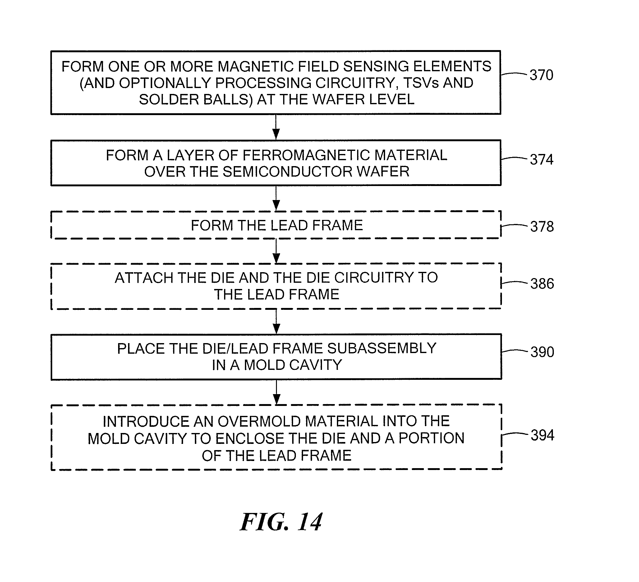
D00014

D00015

D00016
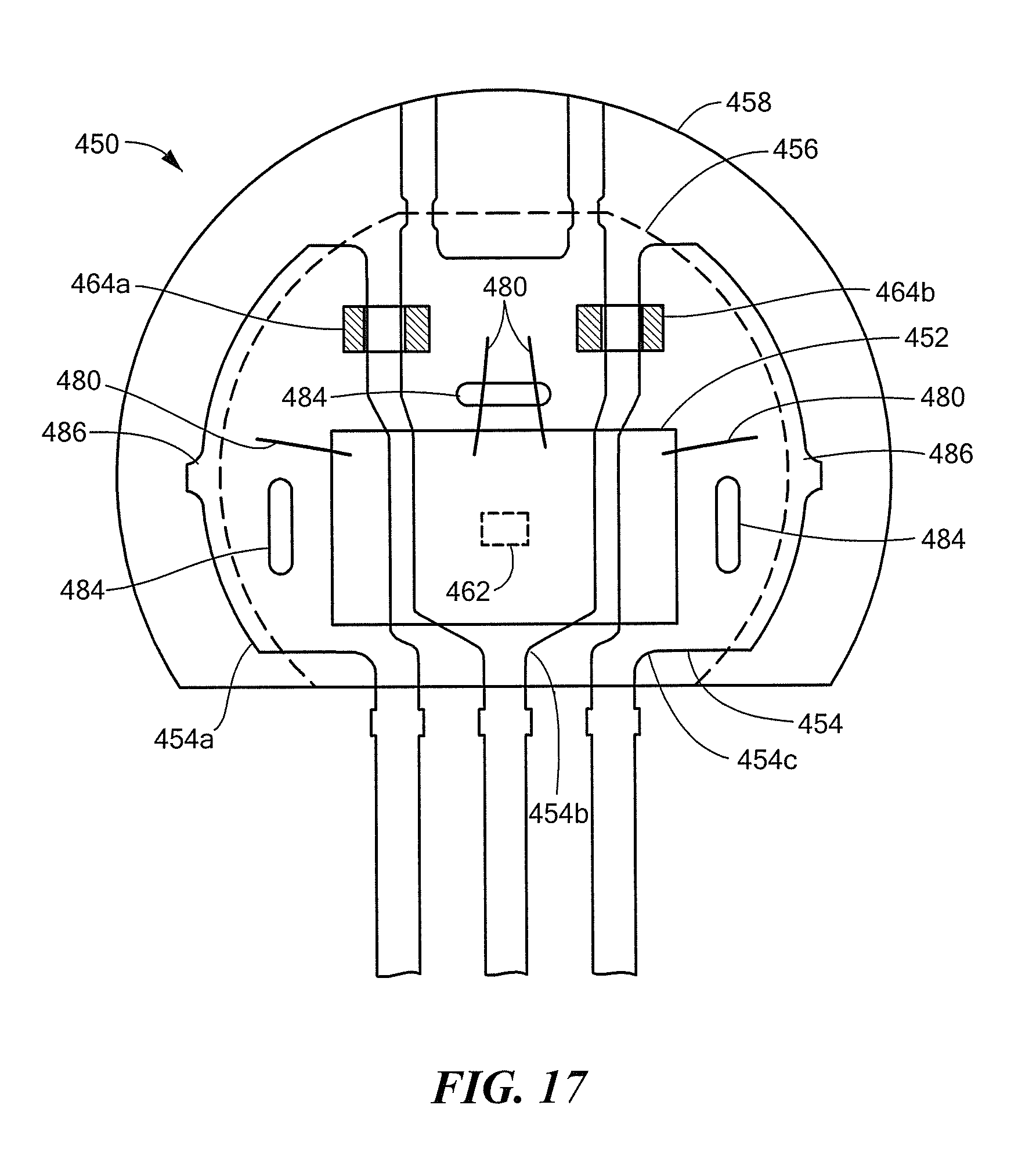
XML
uspto.report is an independent third-party trademark research tool that is not affiliated, endorsed, or sponsored by the United States Patent and Trademark Office (USPTO) or any other governmental organization. The information provided by uspto.report is based on publicly available data at the time of writing and is intended for informational purposes only.
While we strive to provide accurate and up-to-date information, we do not guarantee the accuracy, completeness, reliability, or suitability of the information displayed on this site. The use of this site is at your own risk. Any reliance you place on such information is therefore strictly at your own risk.
All official trademark data, including owner information, should be verified by visiting the official USPTO website at www.uspto.gov. This site is not intended to replace professional legal advice and should not be used as a substitute for consulting with a legal professional who is knowledgeable about trademark law.