Method and system for driving an active matrix display circuit
Nathan , et al.
U.S. patent number 10,229,647 [Application Number 14/491,885] was granted by the patent office on 2019-03-12 for method and system for driving an active matrix display circuit. This patent grant is currently assigned to Ignis Innovation Inc.. The grantee listed for this patent is Ignis Innovation Inc.. Invention is credited to Gholamreza Chaji, Arokia Nathan.


View All Diagrams
| United States Patent | 10,229,647 |
| Nathan , et al. | March 12, 2019 |
Method and system for driving an active matrix display circuit
Abstract
A method and system for driving an active matrix display is provided. The system includes a drive circuit for a pixel having a light emitting device. The drive circuit includes a drive transistor for driving the light emitting device. The system includes a mechanism for adjusting the gate voltage of the drive transistor.
| Inventors: | Nathan; Arokia (Cambridge, GB), Chaji; Gholamreza (Waterloo, CA) | ||||||||||
|---|---|---|---|---|---|---|---|---|---|---|---|
| Applicant: |
|
||||||||||
| Assignee: | Ignis Innovation Inc.
(Waterloo, CA) |
||||||||||
| Family ID: | 48041792 | ||||||||||
| Appl. No.: | 14/491,885 | ||||||||||
| Filed: | September 19, 2014 |
Prior Publication Data
| Document Identifier | Publication Date | |
|---|---|---|
| US 20150009191 A1 | Jan 8, 2015 | |
Related U.S. Patent Documents
| Application Number | Filing Date | Patent Number | Issue Date | ||
|---|---|---|---|---|---|
| 13649888 | Oct 11, 2012 | 9269322 | |||
| 13413517 | Jan 7, 2014 | 8624808 | |||
| 13243330 | Oct 22, 2013 | 8564513 | |||
| 11651099 | Aug 28, 2012 | 8253665 | |||
| 11651099 | Aug 28, 2012 | 8253665 | |||
Foreign Application Priority Data
| Jan 9, 2006 [CA] | 2535233 | |||
| Jun 27, 2006 [CA] | 2551237 | |||
| Current U.S. Class: | 1/1 |
| Current CPC Class: | G09G 3/3685 (20130101); G09G 3/3233 (20130101); G09G 3/3696 (20130101); G09G 3/3266 (20130101); G09G 2320/043 (20130101); G09G 2300/0819 (20130101); G09G 2300/0861 (20130101); G09G 2320/029 (20130101); G09G 2310/0243 (20130101); G09G 2310/0262 (20130101); G09G 2300/0809 (20130101); G09G 2300/0417 (20130101); G09G 2300/043 (20130101); G09G 2310/0272 (20130101); G09G 2300/0842 (20130101); G09G 2310/0251 (20130101); G09G 2300/0426 (20130101) |
| Current International Class: | G09G 3/36 (20060101); G09G 3/3233 (20160101); G09G 3/3266 (20160101) |
References Cited [Referenced By]
U.S. Patent Documents
| 3506851 | April 1970 | Polkinghorn et al. |
| 3750987 | August 1973 | Gobel |
| 3774055 | November 1973 | Bapat et al. |
| 4090096 | May 1978 | Nagami |
| 4354162 | October 1982 | Wright |
| 4996523 | February 1991 | Bell et al. |
| 5134387 | July 1992 | Smith et al. |
| 5153420 | October 1992 | Hack et al. |
| 5170158 | December 1992 | Shinya |
| 5204661 | April 1993 | Hack et al. |
| 5266515 | November 1993 | Robb et al. |
| 5278542 | January 1994 | Smith et al. |
| 5408267 | April 1995 | Main |
| 5498880 | March 1996 | Lee et al. |
| 5572444 | November 1996 | Lentz et al. |
| 5589847 | December 1996 | Lewis |
| 5619033 | April 1997 | Weisfield |
| 5648276 | July 1997 | Hara et al. |
| 5670973 | September 1997 | Bassetti et al. |
| 5691783 | November 1997 | Numao et al. |
| 5701505 | December 1997 | Yamashita et al. |
| 5714968 | February 1998 | Ikeda |
| 5744824 | April 1998 | Kousai et al. |
| 5745660 | April 1998 | Kolpatzik et al. |
| 5748160 | May 1998 | Shieh et al. |
| 5758129 | May 1998 | Gray et al. |
| 5835376 | November 1998 | Smith et al. |
| 5870071 | February 1999 | Kawahata |
| 5874803 | February 1999 | Garbuzov et al. |
| 5880582 | March 1999 | Sawada |
| 5903248 | May 1999 | Irwin |
| 5917280 | June 1999 | Burrows et al. |
| 5949398 | September 1999 | Kim |
| 5952789 | September 1999 | Stewart et al. |
| 5990629 | November 1999 | Yamada et al. |
| 6023259 | February 2000 | Howard et al. |
| 6069365 | May 2000 | Chow et al. |
| 6091203 | July 2000 | Kawashima et al. |
| 6097360 | August 2000 | Holloman |
| 6100868 | August 2000 | Lee et al. |
| 6144222 | November 2000 | Ho |
| 6229506 | May 2001 | Dawson et al. |
| 6229508 | May 2001 | Kane |
| 6246180 | June 2001 | Nishigaki |
| 6252248 | June 2001 | Sano et al. |
| 6268841 | July 2001 | Cairns et al. |
| 6288696 | September 2001 | Holloman |
| 6307322 | October 2001 | Dawson et al. |
| 6310962 | October 2001 | Chung et al. |
| 6323631 | November 2001 | Juang |
| 6333729 | December 2001 | Ha |
| 6388653 | May 2002 | Goto et al. |
| 6392617 | May 2002 | Gleason |
| 6396469 | May 2002 | Miwa et al. |
| 6414661 | July 2002 | Shen et al. |
| 6417825 | July 2002 | Stewart et al. |
| 6430496 | August 2002 | Smith et al. |
| 6433488 | August 2002 | Bu |
| 6473065 | October 2002 | Fan |
| 6475845 | November 2002 | Kimura |
| 6501098 | December 2002 | Yamazaki |
| 6501466 | December 2002 | Yamagashi et al. |
| 6522315 | February 2003 | Ozawa et al. |
| 6535185 | March 2003 | Kim et al. |
| 6542138 | April 2003 | Shannon et al. |
| 6559839 | May 2003 | Ueno et al. |
| 6580408 | June 2003 | Bae et al. |
| 6583398 | June 2003 | Harkin |
| 6618030 | September 2003 | Kane et al. |
| 6639244 | October 2003 | Yamazaki et al. |
| 6680580 | January 2004 | Sung |
| 6686699 | February 2004 | Yumoto |
| 6690000 | February 2004 | Muramatsu et al. |
| 6693610 | February 2004 | Shannon et al. |
| 6694248 | February 2004 | Smith et al. |
| 6697057 | February 2004 | Koyama et al. |
| 6724151 | April 2004 | Yoo |
| 6734636 | May 2004 | Sanford et al. |
| 6753655 | June 2004 | Shih et al. |
| 6753834 | June 2004 | Mikami et al. |
| 6756741 | June 2004 | Li |
| 6777888 | August 2004 | Kondo |
| 6781567 | August 2004 | Kimura |
| 6788231 | September 2004 | Hsueh |
| 6809706 | October 2004 | Shimoda |
| 6828950 | December 2004 | Koyama |
| 6858991 | February 2005 | Miyazawa |
| 6859193 | February 2005 | Yumoto |
| 6876346 | April 2005 | Anzai et al. |
| 6900485 | May 2005 | Lee |
| 6903734 | June 2005 | Eu |
| 6911960 | June 2005 | Yokoyama |
| 6911964 | June 2005 | Lee et al. |
| 6914448 | July 2005 | Jinno |
| 6919871 | July 2005 | Kwon |
| 6924602 | August 2005 | Komiya |
| 6937220 | August 2005 | Kitaura et al. |
| 6940214 | September 2005 | Komiya et al. |
| 6954194 | October 2005 | Matsumoto et al. |
| 6970149 | November 2005 | Chung et al. |
| 6975142 | December 2005 | Azami et al. |
| 6975332 | December 2005 | Arnold et al. |
| 6995519 | February 2006 | Arnold et al. |
| 7027015 | April 2006 | Booth, Jr. et al. |
| 7034793 | April 2006 | Sekiya et al. |
| 7038392 | May 2006 | Libsch et al. |
| 7057588 | June 2006 | Asano et al. |
| 7061451 | June 2006 | Kimura |
| 7071932 | July 2006 | Libsch et al. |
| 7106285 | September 2006 | Naugler |
| 7112820 | September 2006 | Chang et al. |
| 7113864 | September 2006 | Smith et al. |
| 7122835 | October 2006 | Ikeda et al. |
| 7129914 | October 2006 | Knapp et al. |
| 7164417 | January 2007 | Cok |
| 7224332 | May 2007 | Cok |
| 7248236 | July 2007 | Nathan et al. |
| 7259737 | August 2007 | Ono et al. |
| 7262753 | August 2007 | Tanghe et al. |
| 7274363 | September 2007 | Ishizuka et al. |
| 7310092 | December 2007 | Forrest et al. |
| 7315295 | January 2008 | Kimura |
| 7317434 | January 2008 | Lan et al. |
| 7321348 | January 2008 | Cok et al. |
| 7327357 | February 2008 | Jeong |
| 7333077 | February 2008 | Koyama et al. |
| 7343243 | March 2008 | Smith et al. |
| 7414600 | August 2008 | Nathan et al. |
| 7432991 | October 2008 | Chang |
| 7466166 | December 2008 | Date et al. |
| 7495501 | February 2009 | Iwabuchi et al. |
| 7502000 | March 2009 | Yuki et al. |
| 7515124 | April 2009 | Yaguma et al. |
| 7535449 | May 2009 | Miyazawa |
| 7554512 | June 2009 | Steer |
| 7569849 | August 2009 | Nathan et al. |
| 7595776 | September 2009 | Hashimoto et al. |
| 7604718 | October 2009 | Zhang et al. |
| 7609239 | October 2009 | Chang |
| 7612745 | November 2009 | Yumoto et al. |
| 7619594 | November 2009 | Hu |
| 7619597 | November 2009 | Nathan et al. |
| 7639211 | December 2009 | Miyazawa |
| 7683899 | March 2010 | Hirakata et al. |
| 7688289 | March 2010 | Abe et al. |
| 7760162 | July 2010 | Miyazawa |
| 7808008 | October 2010 | Miyake |
| 7859520 | December 2010 | Kimura |
| 7889159 | February 2011 | Nathan et al. |
| 7903127 | March 2011 | Kwon |
| 7920116 | April 2011 | Woo et al. |
| 7944414 | May 2011 | Shirasaki et al. |
| 7978170 | July 2011 | Park et al. |
| 7989392 | August 2011 | Crockett et al. |
| 7995008 | August 2011 | Miwa |
| 8063852 | November 2011 | Kwak et al. |
| 8102343 | January 2012 | Yatabe |
| 8144081 | March 2012 | Miyazawa |
| 8159007 | April 2012 | Bama et al. |
| 8242979 | August 2012 | Anzai et al. |
| 8253665 | August 2012 | Nathan et al. |
| 8319712 | November 2012 | Nathan et al. |
| 2001/0002703 | June 2001 | Koyama |
| 2001/0009283 | July 2001 | Arao et al. |
| 2001/0026257 | October 2001 | Kimura |
| 2001/0030323 | October 2001 | Ikeda |
| 2001/0040541 | November 2001 | Yoneda et al. |
| 2001/0043173 | November 2001 | Troutman |
| 2001/0045929 | November 2001 | Prache |
| 2001/0052940 | December 2001 | Hagihara et al. |
| 2002/0000576 | January 2002 | Inukai |
| 2002/0011796 | January 2002 | Koyama |
| 2002/0011799 | January 2002 | Kimura |
| 2002/0012057 | January 2002 | Kimura |
| 2002/0030190 | March 2002 | Ohtani et al. |
| 2002/0047565 | April 2002 | Nara et al. |
| 2002/0052086 | May 2002 | Maeda |
| 2002/0080108 | June 2002 | Wang |
| 2002/0084463 | July 2002 | Sanford et al. |
| 2002/0101172 | August 2002 | Bu |
| 2002/0117722 | August 2002 | Osada et al. |
| 2002/0140712 | October 2002 | Ouchi et al. |
| 2002/0158587 | October 2002 | Komiya |
| 2002/0158666 | October 2002 | Azami et al. |
| 2002/0158823 | October 2002 | Zavracky et al. |
| 2002/0171613 | November 2002 | Goto et al. |
| 2002/0186214 | December 2002 | Siwinski |
| 2002/0190971 | December 2002 | Nakamura et al. |
| 2002/0195967 | December 2002 | Kim et al. |
| 2002/0195968 | December 2002 | Sanford et al. |
| 2003/0001828 | January 2003 | Asano |
| 2003/0020413 | January 2003 | Oomura |
| 2003/0030603 | February 2003 | Shimoda |
| 2003/0062524 | April 2003 | Kimura |
| 2003/0062844 | April 2003 | Miyazawa |
| 2003/0076048 | April 2003 | Rutherford |
| 2003/0090445 | May 2003 | Chen et al. |
| 2003/0090447 | May 2003 | Kimura |
| 2003/0090481 | May 2003 | Kimura |
| 2003/0095087 | May 2003 | Libsch |
| 2003/0098829 | May 2003 | Chen et al. |
| 2003/0107560 | June 2003 | Yumoto et al. |
| 2003/0107561 | June 2003 | Uchino et al. |
| 2003/0111966 | June 2003 | Mikami et al. |
| 2003/0112205 | June 2003 | Yamada |
| 2003/0112208 | June 2003 | Okabe et al. |
| 2003/0117348 | June 2003 | Knapp et al. |
| 2003/0122474 | July 2003 | Lee |
| 2003/0122747 | July 2003 | Shannon et al. |
| 2003/0128199 | July 2003 | Kimura |
| 2003/0151569 | August 2003 | Lee et al. |
| 2003/0156104 | August 2003 | Morita |
| 2003/0169241 | September 2003 | LeChevalier |
| 2003/0169247 | September 2003 | Kawabe et al. |
| 2003/0174152 | September 2003 | Noguchi |
| 2003/0179626 | September 2003 | Sanford et al. |
| 2003/0185438 | October 2003 | Osawa et al. |
| 2003/0189535 | October 2003 | Matsumoto et al. |
| 2003/0197663 | October 2003 | Lee et al. |
| 2003/0214465 | November 2003 | Kimura |
| 2003/0227262 | December 2003 | Kwon |
| 2003/0230141 | December 2003 | Gilmour et al. |
| 2003/0230980 | December 2003 | Forrest et al. |
| 2004/0004589 | January 2004 | Shih |
| 2004/0032382 | February 2004 | Cok et al. |
| 2004/0041750 | March 2004 | Abe |
| 2004/0066357 | April 2004 | Kawasaki |
| 2004/0070557 | April 2004 | Asano et al. |
| 2004/0070558 | April 2004 | Cok |
| 2004/0129933 | July 2004 | Nathan et al. |
| 2004/0135749 | July 2004 | Kondakov et al. |
| 2004/0145547 | July 2004 | Oh |
| 2004/0150595 | August 2004 | Kasai |
| 2004/0155841 | August 2004 | Kasai |
| 2004/0160516 | August 2004 | Ford |
| 2004/0171619 | September 2004 | Libsch et al. |
| 2004/0174349 | September 2004 | Libsch |
| 2004/0174354 | September 2004 | Ono |
| 2004/0183759 | September 2004 | Stevenson et al. |
| 2004/0189627 | September 2004 | Shirasaki et al. |
| 2004/0196275 | October 2004 | Hattori |
| 2004/0227697 | November 2004 | Mori |
| 2004/0239696 | December 2004 | Okabe |
| 2004/0251844 | December 2004 | Hashido et al. |
| 2004/0252085 | December 2004 | Miyagawa |
| 2004/0252089 | December 2004 | Ono et al. |
| 2004/0256617 | December 2004 | Yamada et al. |
| 2004/0257353 | December 2004 | Imamura et al. |
| 2004/0257355 | December 2004 | Naugler |
| 2004/0263437 | December 2004 | Hattori |
| 2005/0007357 | January 2005 | Yamashita et al. |
| 2005/0030267 | February 2005 | Tanghe |
| 2005/0052379 | March 2005 | Waterman |
| 2005/0057459 | March 2005 | Miyazawa |
| 2005/0067970 | March 2005 | Libsch et al. |
| 2005/0067971 | March 2005 | Kane |
| 2005/0083270 | April 2005 | Miyazawa |
| 2005/0110420 | May 2005 | Arnold et al. |
| 2005/0110727 | May 2005 | Shin |
| 2005/0123193 | June 2005 | Lamberg et al. |
| 2005/0140610 | June 2005 | Smith et al. |
| 2005/0145891 | July 2005 | Abe |
| 2005/0156831 | July 2005 | Yamazaki et al. |
| 2005/0168416 | August 2005 | Hashimoto et al. |
| 2005/0206590 | September 2005 | Sasaki et al. |
| 2005/0219188 | October 2005 | Kawabe et al. |
| 2005/0243037 | November 2005 | Eom et al. |
| 2005/0248515 | November 2005 | Naugler et al. |
| 2005/0258867 | November 2005 | Miyazawa |
| 2005/0285825 | December 2005 | Eom et al. |
| 2006/0012311 | January 2006 | Ogawa |
| 2006/0038750 | February 2006 | Inoue et al. |
| 2006/0038758 | February 2006 | Routley et al. |
| 2006/0038762 | February 2006 | Chou |
| 2006/0066533 | March 2006 | Sato et al. |
| 2006/0077077 | April 2006 | Kwon |
| 2006/0082523 | April 2006 | Guo et al. |
| 2006/0125408 | June 2006 | Nathan et al. |
| 2006/0139253 | June 2006 | Choi et al. |
| 2006/0145964 | July 2006 | Park et al. |
| 2006/0191178 | August 2006 | Sempel et al. |
| 2006/0209012 | September 2006 | Hagood, IV |
| 2006/0214888 | September 2006 | Schneider et al. |
| 2006/0221009 | October 2006 | Miwa |
| 2006/0227082 | October 2006 | Ogata et al. |
| 2006/0232522 | October 2006 | Roy et al. |
| 2006/0244391 | November 2006 | Shishido et al. |
| 2006/0244697 | November 2006 | Lee et al. |
| 2006/0261841 | November 2006 | Fish |
| 2006/0290614 | December 2006 | Nathan et al. |
| 2007/0001939 | January 2007 | Hashimoto et al. |
| 2007/0001945 | January 2007 | Yoshida et al. |
| 2007/0008251 | January 2007 | Kohno et al. |
| 2007/0008297 | January 2007 | Bassetti |
| 2007/0035707 | February 2007 | Margulis |
| 2007/0040773 | February 2007 | Lee et al. |
| 2007/0040782 | February 2007 | Woo et al. |
| 2007/0057874 | March 2007 | Le Roy et al. |
| 2007/0063932 | March 2007 | Nathan et al. |
| 2007/0075957 | April 2007 | Chen |
| 2007/0080908 | April 2007 | Nathan et al. |
| 2007/0085801 | April 2007 | Park et al. |
| 2007/0109232 | May 2007 | Yamamoto et al. |
| 2007/0128583 | June 2007 | Miyazawa |
| 2007/0164941 | July 2007 | Park et al. |
| 2007/0182671 | August 2007 | Nathan et al. |
| 2007/0236430 | October 2007 | Fish |
| 2007/0236440 | October 2007 | Wacyk et al. |
| 2007/0241999 | October 2007 | Lin |
| 2007/0242008 | October 2007 | Cummings |
| 2008/0001544 | January 2008 | Murakami et al. |
| 2008/0043044 | February 2008 | Woo et al. |
| 2008/0048951 | February 2008 | Naugler et al. |
| 2008/0055134 | March 2008 | Li et al. |
| 2008/0088549 | April 2008 | Nathan et al. |
| 2008/0094426 | April 2008 | Kimpe |
| 2008/0111766 | May 2008 | Uchino et al. |
| 2008/0122819 | May 2008 | Cho et al. |
| 2008/0129906 | June 2008 | Lin et al. |
| 2008/0198103 | August 2008 | Toyomura et al. |
| 2008/0228562 | September 2008 | Smith et al. |
| 2008/0231625 | September 2008 | Minami et al. |
| 2008/0231641 | September 2008 | Miyashita |
| 2008/0265786 | October 2008 | Koyama |
| 2008/0290805 | November 2008 | Yamada et al. |
| 2009/0009459 | January 2009 | Miyashita |
| 2009/0015532 | January 2009 | Katayama et al. |
| 2009/0058789 | March 2009 | Hung et al. |
| 2009/0121988 | May 2009 | Amo et al. |
| 2009/0146926 | June 2009 | Sung et al. |
| 2009/0153448 | June 2009 | Tomida et al. |
| 2009/0153459 | June 2009 | Han et al. |
| 2009/0174628 | July 2009 | Wang et al. |
| 2009/0201230 | August 2009 | Smith |
| 2009/0201281 | August 2009 | Routley et al. |
| 2009/0206764 | August 2009 | Schemmann et al. |
| 2009/0244046 | October 2009 | Seto |
| 2009/0251486 | October 2009 | Sakakibara et al. |
| 2009/0278777 | November 2009 | Wang et al. |
| 2009/0289964 | November 2009 | Miyachi |
| 2010/0039451 | February 2010 | Jung |
| 2010/0039453 | February 2010 | Nathan et al. |
| 2010/0079419 | April 2010 | Shibusawa |
| 2010/0207920 | August 2010 | Chaji et al. |
| 2010/0225634 | September 2010 | Levey et al. |
| 2010/0251295 | September 2010 | Amento et al. |
| 2010/0269889 | October 2010 | Reinhold et al. |
| 2010/0277400 | November 2010 | Jeong |
| 2010/0315319 | December 2010 | Cok et al. |
| 2011/0050741 | March 2011 | Jeong |
| 2011/0063197 | March 2011 | Chung et al. |
| 2011/0069089 | March 2011 | Kopf et al. |
| 2011/0169805 | July 2011 | Yamazaki |
| 2012/0169793 | July 2012 | Nathan |
| 2012/0299976 | November 2012 | Chen et al. |
| 729652 | Jun 1997 | AU | |||
| 764896 | Dec 2001 | AU | |||
| 1 294 034 | Jan 1992 | CA | |||
| 2 249 592 | Jul 1998 | CA | |||
| 2 303 302 | Mar 1999 | CA | |||
| 2 368 386 | Sep 1999 | CA | |||
| 2 242 720 | Jan 2000 | CA | |||
| 2 354 018 | Jun 2000 | CA | |||
| 2 432 530 | Jul 2002 | CA | |||
| 2 436 451 | Aug 2002 | CA | |||
| 2 507 276 | Aug 2002 | CA | |||
| 2 463 653 | Jan 2004 | CA | |||
| 2 498 136 | Mar 2004 | CA | |||
| 2 522 396 | Nov 2004 | CA | |||
| 2 438 363 | Feb 2005 | CA | |||
| 2 443 206 | Mar 2005 | CA | |||
| 2 519 097 | Mar 2005 | CA | |||
| 2 472 671 | Dec 2005 | CA | |||
| 2 523 841 | Jan 2006 | CA | |||
| 2 567 076 | Jan 2006 | CA | |||
| 2 495 726 | Jul 2006 | CA | |||
| 2 557 713 | Nov 2006 | CA | |||
| 2 526 782 | Aug 2007 | CA | |||
| 2 651 893 | Nov 2007 | CA | |||
| 2 672 590 | Oct 2009 | CA | |||
| 1601594 | Mar 2005 | CN | |||
| 1700285 | Nov 2005 | CN | |||
| 1886774 | Dec 2006 | CN | |||
| 101395653 | Mar 2009 | CN | |||
| 102129842 | Jul 2011 | CN | |||
| 202006007613 | Sep 2006 | DE | |||
| 0 478 186 | Apr 1992 | EP | |||
| 1 028 471 | Aug 2000 | EP | |||
| 1 130 565 | Sep 2001 | EP | |||
| 1 194 013 | Apr 2002 | EP | |||
| 1 321 922 | Jun 2003 | EP | |||
| 1 335 430 | Aug 2003 | EP | |||
| 1 381 019 | Jan 2004 | EP | |||
| 1 429 312 | Jun 2004 | EP | |||
| 1 439 520 | Jul 2004 | EP | |||
| 1 465 143 | Oct 2004 | EP | |||
| 1 473 689 | Nov 2004 | EP | |||
| 1 517 290 | Mar 2005 | EP | |||
| 1 521 203 | Apr 2005 | EP | |||
| 2 399 935 | Sep 2004 | GB | |||
| 2 460 018 | Nov 2009 | GB | |||
| 09 090405 | Apr 1997 | JP | |||
| 10-254410 | Sep 1998 | JP | |||
| 11 231805 | Aug 1999 | JP | |||
| 2002-278513 | Sep 2002 | JP | |||
| 2003-076331 | Mar 2003 | JP | |||
| 2003-099000 | Apr 2003 | JP | |||
| 2003-173165 | Jun 2003 | JP | |||
| 2003-186439 | Jul 2003 | JP | |||
| 2003-195809 | Jul 2003 | JP | |||
| 2003-271095 | Sep 2003 | JP | |||
| 2003-308046 | Oct 2003 | JP | |||
| 2004-054188 | Feb 2004 | JP | |||
| 2004-226960 | Aug 2004 | JP | |||
| 2005-004147 | Jan 2005 | JP | |||
| 2005-099715 | Apr 2005 | JP | |||
| 2005-258326 | Sep 2005 | JP | |||
| 2005-338819 | Dec 2005 | JP | |||
| 569173 | Jan 2004 | TW | |||
| 200526065 | Aug 2005 | TW | |||
| 1239501 | Sep 2005 | TW | |||
| WO 98/11554 | Mar 1998 | WO | |||
| WO 99/48079 | Sep 1999 | WO | |||
| WO 01/27910 | Apr 2001 | WO | |||
| WO 02/067327 | Aug 2002 | WO | |||
| WO 03/034389 | Apr 2003 | WO | |||
| WO 03/063124 | Jul 2003 | WO | |||
| WO 03/075256 | Sep 2003 | WO | |||
| WO 2004/003877 | Jan 2004 | WO | |||
| WO 2004/015668 | Feb 2004 | WO | |||
| WO 2004/034364 | Apr 2004 | WO | |||
| WO 2005/022498 | Mar 2005 | WO | |||
| WO 2005/055185 | Jun 2005 | WO | |||
| WO 2005/055186 | Jun 2005 | WO | |||
| WO 2005/069267 | Jul 2005 | WO | |||
| WO 2005/122121 | Dec 2005 | WO | |||
| WO 2006/063448 | Jun 2006 | WO | |||
| WO 2006/128069 | Nov 2006 | WO | |||
| WO 2008/057369 | May 2008 | WO | |||
| WO 2008/0290805 | Nov 2008 | WO | |||
| WO 2009/059028 | May 2009 | WO | |||
| WO 2009/127065 | Oct 2009 | WO | |||
| WO 2010/066030 | Jun 2010 | WO | |||
| WO 2010/120733 | Oct 2010 | WO | |||
Other References
|
Ahnood et al.: "Effect of threshold voltage instability on field effect mobility in thin film transistors deduced from constant current measurements"; dated Aug. 2009. cited by applicant . Alexander et al.: "Pixel circuits and drive schemes for glass and elastic AMOLED displays"; dated Jul. 2005 (9 pages). cited by applicant . Alexander et al.: "Unique Electrical Measurement Technology for Compensation Inspection and Process Diagnostics of AMOLED HDTV"; dated May 2010 (4 pages). cited by applicant . Ashtiani et al.: "AMOLED Pixel Circuit With Electronic Compensation of Luminance Degradation"; dated Mar. 2007 (4 pages). cited by applicant . Chaji et al.: "A Current-Mode Comparator for Digital Calibration of Amorphous Silicon AMOLED Displays"; dated Jul. 2008 (5 pages). cited by applicant . Chaji et al.: "A fast settling current driver based on the CCII for AMOLED displays"; dated Dec. 2009 (6 pages). cited by applicant . Chaji et al.: "A Low-Cost Stable Amorphous Silicon AMOLED Display with Full V.about.T--and V.about.O.about.L.about.E.about.D Shift Compensation"; dated May 2007 (4 pages). cited by applicant . Chaji et al.: "A low-power driving scheme for a-Si:H active-matrix organic light-emitting diode displays"; dated Jun. 2005 (4 pages). cited by applicant . Chaji et al.: "A low-power high-performance digital circuit for deep submicron technologies"; dated Jun. 2005 (4 pages). cited by applicant . Chaji et al.: "A novel a-Si:H AMOLED pixel circuit based on short-term stress stability of a-Si:H TFTs"; dated Oct. 2005 (3 pages). cited by applicant . Chaji et al.: "A Novel Driving Scheme and Pixel Circuit for AMOLED Displays"; dated Jun. 2006 (4 pages). cited by applicant . Chaji et al.: "A novel driving scheme for high-resolution large-area a-Si:H AMOLED displays"; dated Aug. 2005 (4 pages). cited by applicant . Chaji et al.: "A Stable Voltage-Programmed Pixel Circuit for a-Si:H AMOLED Displays"; dated Dec. 2006 (12 pages). cited by applicant . Chaji et al.: "A Sub-.mu.A fast-settling current-programmed pixel circuit for AMOLED displays"; dated Sep. 2007. cited by applicant . Chaji et al.: "An Enhanced and Simplified Optical Feedback Pixel Circuit for AMOLED Displays"; dated Oct. 2006. cited by applicant . Chaji et al.: "Compensation technique for DC and transient instability of thin film transistor circuits for large-area devices"; dated Aug. 2008. cited by applicant . Chaji et al.: "Driving scheme for stable operation of 2-TFT a-Si AMOLED pixel"; dated Apr. 2005 (2 pages). cited by applicant . Chaji et al.: "Dynamic-effect compensating technique for stable a-Si:H AMOLED displays"; dated Aug. 2005 (4 pages). cited by applicant . Chaji et al.: "Electrical Compensation of OLED Luminance Degradation"; dated Dec. 2007 (3 pages). cited by applicant . Chaji et al.: "eUTDSP: a design study of a new VLIW-based DSP architecture"; dated May 2003 (4 pages). cited by applicant . Chaji et al.: "Fast and Offset-Leakage Insensitive Current-Mode Line Driver for Active Matrix Displays and Sensors"; dated Feb. 2009 (8 pages). cited by applicant . Chaji et al.: "High Speed Low Power Adder Design With a New Logic Style: Pseudo Dynamic Logic (SDL)"; dated Oct. 2001 (4 pages). cited by applicant . Chaji et al.: "High-precision fast current source for large-area current-programmed a-Si flat panels"; dated Sep. 2006 (4 pages). cited by applicant . Chaji et al.: "Low-Cost AMOLED Television with IGNIS Compensating Technology"; dated May 2008 (4 pages). cited by applicant . Chaji et al.: "Low-Cost Stable a-Si:H AMOLED Display for Portable Applications"; dated Jun. 2006 (4 pages). cited by applicant . Chaji et al.: "Low-Power Low-Cost Voltage-Programmed a-Si:H AMOLED Display"; dated Jun. 2008 (5 pages). cited by applicant . Chaji et al.: "Merged phototransistor pixel with enhanced near infrared response and flicker noise reduction for biomolecular imaging"; dated Nov. 2008 (3 pages). cited by applicant . Chaji et al.: "Parallel Addressing Scheme for Voltage-Programmed Active-Matrix OLED Displays"; dated May 2007 (6 pages). cited by applicant . Chaji et al.: "Pseudo dynamic logic (SDL): a high-speed and low-power dynamic logic family"; dated 2002 (4 pages). cited by applicant . Chaji et al.: "Stable a-Si:H circuits based on short-term stress stability of amorphous silicon thin film transistors"; dated May 2006 (4 pages). cited by applicant . Chaji et al.: "Stable Pixel Circuit for Small-Area High- Resolution a-Si:H AMOLED Displays"; dated Oct. 2008 (6 pages). cited by applicant . Chaji et al.: "Stable RGBW AMOLED display with OLED degradation compensation using electrical feedback"; dated Feb. 2010 (2 pages). cited by applicant . Chaji et al.: "Thin-Film Transistor Integration for Biomedical Imaging and AMOLED Displays"; dated May 2008 (177 pages). cited by applicant . Chapter 3: Color Spaces "Keith Jack: "Video Demystified:" A Handbook for the Digital Engineer" 2001 Referex ORD-0000-00-00 USA EP040425529 ISBN: 1-878707-56-6 pp. 32-33. cited by applicant . Chapter 8: Alternative Flat Panel Display 1-25 Technologies; Willem den Boer: "Active Matrix Liquid Crystal Display: Fundamentals and Applications" 2005 Referex ORD-0000-00-00 U.K.; XP040426102 ISBN: 0-7506-7813-5 pp. 206-209 p. 208. cited by applicant . European Partial Search Report Application No. 12 15 6251.6 European Patent Office dated May 30, 2012 (7 pages). cited by applicant . European Patent Office Communication Application No. 05 82 1114 dated Jan. 11, 2013 (9 pages). cited by applicant . European Patent Office Communication with Supplemental European Search Report for EP Application No. 07 70 1644.2 dated Aug. 18, 2009 (12 pages). cited by applicant . European Search Report Application No. 10 83 4294.0-1903 dated Apr. 8, 2013 (9 pages). cited by applicant . European Search Report Application No. EP 05 80 7905 dated Apr. 2, 2009 (5 pages). cited by applicant . European Search Report Application No. EP 05 82 1114 dated Mar. 27, 2009 (2 pages). cited by applicant . European Search Report Application No. EP 07 70 1644 dated Aug. 5, 2009. cited by applicant . European Search Report Application No. EP 10 17 5764 dated Oct. 18, 2010 (2 pages). cited by applicant . European Search Report Application No. EP 10 82 9593.2 European Patent Office dated May 17, 2013 (7 pages). cited by applicant . European Search Report Application No. EP 12 15 6251.6 European Patent Office dated Oct. 12, 2012 (18 pages). cited by applicant . European Search Report Application No. EP. 11 175 225.9 dated Nov. 4, 2011 (9 pages). cited by applicant . European Supplementary Search Report Application No. EP 09 80 2309 dated May 8, 2011 (14 pages). cited by applicant . European Supplementary Search Report Application No. EP 09 83 1339.8 dated Mar. 26, 2012 (11 pages). cited by applicant . Extended European Search Report Application No. EP 06 75 2777.0 dated Dec. 6, 2010 (21 pages). cited by applicant . Extended European Search Report Application No. EP 09 73 2338.0 dated May 24, 2011 (8 pages). cited by applicant . Extended European Search Report Application No. EP 11 17 5223., 4 dated Nov. 8, 2011 (8 pages). cited by applicant . Extended European Search Report Application No. EP 12 17 4465.0 European Patent Office dated Sep. 7, 2012 (9 pages). cited by applicant . Fan et al. "LTPS_TFT Pixel Circuit Compensation for TFT Threshold Voltage Shift and IR-Drop on the Power Line for Amolded Displays" 5 pages copyright 2012. cited by applicant . Goh et al. "A New a-Si:H Thin-Film Transistor Pixel Circuit for Active-Matrix Organic Light-Emitting Diodes" IEEE Electron Device Letters vol. 24 No. 9 Sep. 2003 pp. 583-585. cited by applicant . International Search Report Application No. PCT/CA2005/001844 dated Mar. 28, 2006 (2 pages). cited by applicant . International Search Report Application No. PCT/CA2006/000941 dated Oct. 3, 2006 (2 pages). cited by applicant . International Search Report Application No. PCT/CA2007/000013 dated May 7, 2007. cited by applicant . International Search Report Application No. PCT/CA2009/001049 dated Dec. 7, 2009 (4 pages). cited by applicant . International Search Report Application No. PCT/CA2009/001769 dated Apr. 8, 2010. cited by applicant . International Search Report Application No. PCT/IB2010/002898 Canadian Intellectual Property Office dated Jul. 28, 2009 (5 pages). cited by applicant . International Search Report Application No. PCT/IB2010/055481 dated Apr. 7, 2011 (3 pages). cited by applicant . International Search Report Application No. PCT/IB2011/051103 dated Jul. 8, 2011 3 pages. cited by applicant . International Search Report Application No. PCT/IB2012/052651 5 pages dated Sep. 11, 2012. cited by applicant . International Searching Authority Written Opinion Application No. PCT/IB2010/055481 dated Apr. 7, 2011 (6 pages ). cited by applicant . International Searching Authority Written Opinion Application No. PCT/IB2012/052651 6 pages dated Sep. 11, 2012. cited by applicant . International Searching Authority Written Opinion Application No. PCT/IB2011/051103 dated Jul. 8, 2011 6 pages. cited by applicant . International Searching Authority Written Opinion Application No. PCT/IB2010/002898 Canadian Intellectual Property Office dated Mar. 30, 2011 (8 pages). cited by applicant . International Searching Authority Written Opinion Application No. PCT/CA2009/001769 dated Apr. 8, 2010 (8 pages). cited by applicant . Jafarabadiashtiani et al.: "A New Driving Method for a-Si AMOLED Displays Based on Voltage Feedback"; dated May 2005 (4 pages). cited by applicant . Lee et al.: "Ambipolar Thin-Film Transistors Fabricated by PECVD Nanocrystalline Silicon"; dated May 2006 (6 pages). cited by applicant . Ma e y et al: "Organic Light-Emitting Diode/Thin Film Transistor Integration for foldable Displays" Conference record of the 1997 International display research conference and international workshops on LCD technology and emissive technology. Toronto Sep. 15-19, 1997 (6 pages). cited by applicant . Matsueda y et al.: "35.1: 2.5-in. AMOLED with Integrated 6-bit Gamma Compensated Digital Data Driver"; dated May 2004 (4 pages). cited by applicant . Nathan et al. "Amorphous Silicon Thin Film Transistor Circuit Integration for Organic LED Displays on Glass and Plastic" IEEE Journal of Solid-State Circuits vol. 39 No. 9 Sep. 2004 pp. 1477-1486. cited by applicant . Nathan et al.: "Backplane Requirements for Active Matrix Organic Light Emitting Diode Displays"; dated Sep. 2006 (16 pages). cited by applicant . Nathan et al.: "Call for papers second international workshop on compact thin-film transistor (TFT) modeling for circuit simulation"; dated Sep. 2009 (1 page). cited by applicant . Nathan et al.: "Driving schemes for a-Si and LTPS AMOLED displays"; dated Dec. 2005 (11 pages). cited by applicant . Nathan et al.: "Invited Paper: a -Si for AMOLED--Meeting the Performance and Cost Demands of Display Applications (Cell Phone to HDTV)"; dated Jun. 2006 (4 pages). cited by applicant . Nathan et al.: "Thin film imaging technology on glass and plastic"; dated Oct. 31-Nov. 2, 2000 (4 pages). cited by applicant . Ono et al. "Shared Pixel Compensation Circuit for AM-OLED Displays " Proceedings of the 9.sup.th Asian Symposium on Information Display (ASID) pp. 462-465 New Delhi dated Oct. 8-12, 2006 (4 pages). cited by applicant . Philipp: "Charge transfer sensing" Sensor Review vol. 19 No. 2 Dec. 31, 1999 (Dec. 31, 1999) 10 pages. cited by applicant . Rafati et al.: "Comparison of a 17 b multiplier in Dual-rail domino and in Dual-rail D L (D L) logic styles"; dated 2002 (4 pages). cited by applicant . Safavaian et al.: "Three-TFT image sensor for real-time digital X-ray imaging"; dated Feb. 2, 2006 (2 pages). cited by applicant . Safavian et al.: "3-TFT active pixel sensor with correlated double sampling readout circuit for real-time medical x-ray imaging"; dated Jun. 2006 (4 pages). cited by applicant . Safavian et al.: "A novel current scaling active pixel sensor with correlated double sampling readout circuit for real time medical x-ray imaging"; dated May 2007 (7 pages). cited by applicant . Safavian et al.: "A novel hybrid active-passive pixel with correlated double sampling CMOS readout circuit for medical x-ray imaging"; dated May 2008 (4 pages). cited by applicant . Safavian et al.: "Self-compensated a-Si:H detector with current-mode readout circuit for digital X-ray fluoroscopy"; dated Aug. 2005 (4 pages). cited by applicant . Safavian et al.: "TFT active image sensor with current-mode readout circuit for digital x-ray fluoroscopy [5969D-82]"; dated Sep. 2005 (9 pages). cited by applicant . Smith, Lindsay I., "A tutorial on Principal Components Analysis," dated Feb. 26, 2001 (27 pages). cited by applicant . Stewart M. et al. "Polysilicon TFT technology for active matrix OLED displays" IEEE transactions on electron devices vol. 48 No. 5 May 2001 (7 pages). cited by applicant . Vygranenko et al.: "Stability of indium-oxide thin-film transistors by reactive ion beam assisted deposition"; dated Feb. 2009. cited by applicant . Wang et al.: "Indium oxides by reactive ion beam assisted evaporation: From material study to device application," dated Mar. 2009 (6 pages). cited by applicant . Yi He et al. "Current-Source a-Si:H Thin Film Transistor Circuit for Active-Matrix Organic Light-Emitting Displays" IEEE Electron Device Letters vol. 21 No. 12 Dec. 2000 pp. 590-592. cited by applicant . International Search Report Application No. PCT/IB2013/059074, dated Dec. 18, 2013 (5 pages). cited by applicant . Extended European Search Report for Application No. EP 13845041.6, dated May 30, 2016 (9 pages). cited by applicant . International Search Report for Application No. PCT/IB2017/050170, dated May 5, 2017 (3 pages). cited by applicant . Written Opinion for Application No. PCT/IB2017/050170, dated May 5, 2017 (4 pages). cited by applicant. |
Primary Examiner: Boddie; William
Assistant Examiner: Elnafia; Saifeldin E
Attorney, Agent or Firm: Stratford Managers Corporation
Parent Case Text
CROSS-REFERENCE TO RELATED APPLICATION(S)
This application is a continuation of application Ser. No. 13/649,888, filed Oct. 11, 2012, which is a continuation-in-part of application Ser. No. 13/413,517, filed Mar. 6, 2012, now U.S. Pat. No. 8,624,808, and application Ser. No. 13/243,330, filed Sep. 23, 2011, now U.S. Pat. No. 8,564,513, application Ser. Nos. 13/413,517 and 13/243,330 are both continuations of application Ser. No. 11/651,099, filed Jan. 9, 2007, now U.S. Pat. No. 8,253,665, each of the above noted applications is hereby incorporated by reference herein in its entirety. This application further claims priority to Canadian Patent Application No. 2,535,233, filed on Jan. 9, 2006, and Canadian Application No. 2,551,237, filed on Jun. 27, 2006, each of which is hereby incorporated by reference herein in its entirety.
Claims
What is claimed is:
1. A display comprising: an array of pixel circuits arranged in rows and columns, each of the pixel circuits including: a light emitting device for emitting light; and a drive circuit for driving the light emitting device; a temperature sensor associated with at least one pixel circuit and having a sensing terminal coupled to an internal node of a first pixel circuit of the at least one pixel circuit, the drive circuit of the first pixel circuit coupled directly to the internal node, a conductance of the temperature sensor depending upon the temperature of the first pixel circuit, a changing voltage of the internal node discharging through the temperature sensor based on the conductance of the temperature sensor constituting a time-varying sensor output of the temperature sensor, a read-back circuit controllably coupled to said temperature sensor via said internal node and producing a time-varying output signal based on said time-varying sensor output when coupled to said temperature sensor, said internal node being interposed between said temperature sensor and said read-back circuit, at least one controllable switch coupling said read-back circuit to said temperature sensor, and, a data driver circuit coupled to said read-back circuit and to said pixels and providing programming signals to said pixels based in part on variations in said time-varying output signal from said read-back circuit.
2. The display of claim 1, wherein the temperature sensor is shared between two or more of the pixel circuits.
3. The display of claim 1, wherein the sensing terminal of the temperature sensor is controllably coupled to the internal node of the pixel circuit.
4. The display of claim 1, wherein the time-varying output signal of the read-back circuit is used to compensate for the change in the characteristics of the pixel circuit by calibrating a programming voltage stored in a storage capacitor of the pixel circuit.
5. The display of claim 4, which includes a data line controllably coupled to said storage capacitor via said internal node.
6. The display of claim 1, which includes multiple temperature sensors associated with different pixels or groups of pixels, and multiple read-back circuits, each of which is coupled to a different temperature sensor.
7. The display of claim 6, wherein the time-varying output signal of the read-back circuit is used to compensate for the change in the characteristics of the pixel circuit by calibrating a programming voltage stored in a storage capacitor of the pixel circuit.
8. The display of claim 1, in which the programming signals are calibrated based on the time-varying output signal of the read-back circuit.
9. The display of claim 1, in which the data driver circuit generates programming data, calibrates the programming data, and drives data lines to the pixels with the calibrated programming data.
10. The display of claim 1, wherein said programming signals compensate for the change in the temperature of the pixel circuit.
Description
FIELD OF INVENTION
The invention relates to a light emitting device, and more specifically to a method and system for driving a pixel circuit having a light emitting device.
BACKGROUND OF THE INVENTION
Electro-luminance displays have been developed for a wide variety of devices, such as cell phones. In particular, active-matrix organic light emitting diode (AMOLED) displays with amorphous silicon (a-Si), poly-silicon, organic, or other driving backplane have become more attractive clue to advantages, such as feasible flexible displays, its low cost fabrication, high resolution, and a wide viewing angle.
An AMOLED display includes an array of rows and columns of pixels, each having an organic light emitting diode (OLED) and backplane electronics arranged in the array of rows and columns. Since the OLED is a current driven device, the pixel circuit of the AMOLED should be capable of providing an accurate and constant drive current
There is a need to provide a method and system that is capable of providing constant brightness with high accuracy and reducing the effect of the aging of the pixel circuit and the instability of backplane and a light emitting device.
SUMMARY OF THE INVENTION
It is an object of the invention to provide a method and system that obviates or mitigates at least one of the disadvantages of existing systems.
In accordance with an aspect of the present invention there is provided a system a display system, including a drive circuit for a pixel having a light emitting device. The drive circuit includes a drive transistor connected to the light emitting device. The drive transistor includes a gate terminal, a first terminal and a second terminal. The drive circuit includes a first transistor including a gate terminal, a first terminal and a second terminal, the gate terminal of the first transistor being connected to a select line, the first terminal of the first transistor being connected to a data line, the second terminal of the first transistor being connected to the gate terminal of the drive transistor. The drive circuit includes a circuit for adjusting the gate voltage of the drive transistor, the circuit including a discharging transistor having a gate terminal, a first terminal and a second terminal, the gate terminal of the discharging transistor being connected to the gate terminal of the drive transistor at a node, the voltage of the node being discharged through the discharging transistor. The drive circuit includes a storage capacitor including a first terminal and a second terminal, the first terminal of the storage capacitor being connected to the gate terminal of the drive transistor at the node.
The display system may include a display array having a plurality of pixel circuits arranged in rows and columns, each of the pixel circuits including the drive circuit, and a driver for driving the display array. The gate terminal of the second transistor is connected to a bias line. The bias line may be shared by more than one pixel circuit of the plurality of pixel circuits.
In accordance with a further aspect of the present invention there is provided a method for the display system. The display system includes a driver for providing a programming cycle, a compensation cycle and a driving cycle for each row. The method includes the steps of at the programming cycle for a first row, selecting the address line for the first row and providing programming data to the first row, at the compensation cycle for the first row, selecting the adjacent address line for a second row adjacent to the first row and disenabling the address line for the first row, and at the driving cycle for the first row, disenabling the adjacent address line.
In accordance with a further aspect of the present invention there is provided a display system, including one or more than one pixel circuit, each including a light emitting device and a drive circuit. The drive circuit includes a drive transistor including a gate terminal, a first terminal and a second terminal, the drive transistor being between the light emitting device and a first power supply. The drive circuit includes a switch transistor including a gate terminal, a first terminal and a second terminal, the gate terminal of the switch transistor being connected to a first address line, the first terminal of the switch transistor being connected to a data line, the second terminal of the switch transistor being connected to the gate terminal of the drive transistor. The drive circuit includes a circuit for adjusting the gate voltage of the drive transistor, the circuit including a sensor for sensing energy transfer from the pixel circuit and a discharging transistor, the sensor having a first terminal and a second terminal, a property of the sensor varying in dependence upon the sensing result, the discharging transistor having a gate terminal, a first terminal and a second terminal, the gate terminal of the discharging transistor being connected to a second address line, the first terminal of the discharging: transistor being connected to the gate terminal of the drive transistor at a node, the second terminal of the discharging transistor being connected to the first terminal of the sensor, The drive circuit includes a storage capacitor including a first terminal and a second terminal, the first terminal of the storage capacitor being connected to the gate terminal of the drive transistor at the node.
In accordance with a further aspect of the present invention there is provided a method for a display system, including the step of implementing an in-pixel compensation.
In accordance with a further aspect of the present invention there is provided a method for a display system, including the step of implementing an of-panel compensation
In accordance with a further aspect of the present invention there is provided a method for a display system, which includes a pixel circuit having a sensor, including the step of reading back the aging of the sensor.
In accordance with a further aspect of the present invention there is provided a display system, including a display array including a plurality of pixel circuits arranged in rows and columns, each including a light emitting device and a drive circuit; and a drive system for driving the display array. The drive circuit includes a drive transistor including a gate terminal, a first terminal and a second terminal, the drive transistor being between the light emitting device and a first power supply. The drive circuit includes a first transistor including a gate terminal, a first terminal and a second terminal, the gate terminal of the first transistor being connected to an address line, the first terminal of the fast transistor being connected to a data line, the second terminal of the first transistor being connected to the gate terminal of the drive transistor. The drive circuit includes a circuit for adjusting the voltage of the drive transistor, the circuit including a second transistor, the second transistor having a gate terminal, a first terminal and a second terminal, the gate terminal of the second transistor being connected to a control line, the first terminal of the second transistor being connected to the gate terminal of the drive transistor. The drive circuit includes a storage capacitor including a first terminal and a second terminal, the first terminal of the storage capacitor being connected to the gate terminal of the drive transistor, The drive system drives the pixel circuit so that the pixel circuit is turned off for a portion of a frame time.
In accordance with a further aspect of the present invention there is provided a method for a display system having a display array and a driver system. The drive system provides a frame time having a programming cycle, a discharge cycle, an emission cycle, a reset cycle, and a relaxation cycle, for each row. The method includes the steps of at the programming cycle, programming the pixel circuits on the row by activating the address line for the row; at the discharge cycle, partially discharging the voltage on the gate terminal of the drive transistor by deactivating the address line for the row and activating the control line for the row; at the emission cycle, deactivating the control line for the row, and controlling the light emitting device by the drive transistor; at the reset cycle, discharging the voltage on the gate terminal of the drive transistor by activating the control line for the row; and at the relaxation cycle, deactivating the control line for the row.
BRIEF DESCRIPTION OF THE DRAWINGS
These and other features of the invention will become more apparent from the following description in which reference is made to the appended drawings wherein:
FIG. 1 is a diagram illustrating an example of a pixel circuit to which a pixel drive scheme in accordance with an embodiment of the present invention is applied;
FIG. 2 is a diagram illustrating another example of a pixel circuit having a drive circuit of FIG. 1;
FIG. 3 is a timing diagram for an example of a method of driving a pixel circuit in accordance with an embodiment of the present invention;
FIG. 4 is a diagram illustrating an example of a display system for the drive circuit of FIGS. 1 and 2;
FIG. 5 is a diagram illustrating an example of a pixel circuit to which a pixel drive scheme in accordance with another embodiment of the present invention is applied;
FIG. 6 is a diagram illustrating another example of a drive circuit of FIG. 5;
FIG. 7 is a diagram illustrating a further example of the drive circuit of FIG. 5;
FIG. 8 is a diagram illustrating another example of a pixel circuit having the drive circuit of FIG. 5;
FIG. 9 is a timing diagram for an example of a method of driving a pixel circuit in accordance with another embodiment of the present invention;
FIG. 10 is a diagram illustrating an example of a display system for the drive circuit of FIGS. 5 and 8;
FIG. 11 is a diagram illustrating an example of a display system for the drive circuit of FIGS. 6 and 7;
FIG. 12 is a graph illustrating simulation results for the pixel circuit of FIG. 1;
FIG. 13 is a diagram illustrating an example of a pixel circuit to which a pixel drive scheme in accordance with a further embodiment of the present invention is applied;
FIG. 14 is a diagram illustrating another example of a pixel circuit having a drive circuit of FIG. 13;
FIG. 15 is a timing diagram for an example of a method of driving a pixel circuit in accordance with a further embodiment of the present invention;
FIG. 16 is a diagram illustrating an example of a display system for the drive circuit of FIGS. 13 and 14;
FIG. 17 is a graph illustrating simulation results for the pixel circuit of FIG. 5;
FIG. 18 is a graph illustrating simulation results for the pixel circuit of FIG. 5;
FIG. 19 is a timing diagram for the operation of the display system of FIG. 16.
FIG. 20 is a diagram illustrating an example of a pixel circuit to which a pixel drive scheme in accordance with a further embodiment of the present invention is applied;
FIG. 21 is a diagram illustrating another example of a pixel circuit having the drive circuit of FIG. 20;
FIG. 22 is a timing diagram illustrating an example of a method of driving a pixel circuit in accordance with a further embodiment of the present invention;
FIG. 23 is a diagram illustrating an example of a display system for the drive circuit of FIGS. 20 and 21;
FIG. 24 is a diagram illustrating another example of a display system for the drive circuit of FIGS. 20 and 21;
FIG. 25 is a diagram illustrating an example of a pixel system in accordance with as embodiment of the present invention;
FIG. 26 is a diagram illustrating an example of a display system having a read back circuit of FIG. 25;
FIG. 27 is a diagram illustrating another example of a display system having the read back circuit of FIG. 25;
FIG. 28 is a timing diagram illustrating an example of a method of driving a pixel circuit in accordance with a further embodiment of the present invention;
FIG. 29 is a diagram illustrating an example of a method of extracting the aging of a sensor of FIG. 25;
FIG. 30 is a diagram illustrating an example of a pixel system in accordance with another embodiment of the present invention;
FIG. 31 is a diagram illustrating an example of a display system having a read back circuit of FIG. 30;
FIG. 32 is a diagram illustrating another example of a display system having the read back circuit of FIG. 30;
FIG. 33 is a timing diagram illustrating an example of a method of driving a pixel circuit in accordance with a further embodiment of the present invention;
FIG. 34 is a timing diagram illustrating another example of a method of extracting the aging of a sensor of FIG. 30;
FIG. 35 is a diagram illustrating an example of a pixel circuit to which a pixel drive scheme in accordance with a further embodiment of the present invention is applied;
FIG. 36 is a timing diagram for an example of a method of driving a pixel circuit in accordance with a further embodiment of the present invention;
FIG. 37 is a diagram illustrating an example of a display system having the pixel circuit of FIG. 35;
FIG. 38 is a diagram illustrating another example of a display system having the pixel circuit of FIG. 35;
FIG. 39 is a diagram illustrating an example of a pixel circuit to which a pixel drive scheme in accordance with another embodiment of the present invention is applied;
FIG. 40 is a diagram illustrating an example of a pixel circuit to which a pixel drive scheme in accordance with a further embodiment of the present invention is applied; and
FIG. 41 is a diagram illustrating an example of a pixel circuit to which a pixel drive scheme in accordance with another embodiment of the present invention is applied.
DETAILED DESCRIPTION
FIG. 1 illustrates an example of a pixel circuit to which a pixel drive scheme in accordance with an embodiment of the present invention is applied. The pixel circuit 100 of FIG. 1 includes an OLED 102 and a drive circuit 104 for driving the OLED 102. The drive circuit 104 includes a drive transistor 106, a discharging transistor 108, a switch transistor 110, and a storage capacitor 112. The OLED 102 includes, for example, an anode electrode, a cathode electrode and an emission layer between the anode electrode and the cathode electrode.
In the description below, "pixel circuit" and "pixel" are used interchangeably. In the description below, "signal" and "line" may be used interchangeably. In the description below, the terms "line" and "node" may be used interchangeably. In the description, the terms "select line" and "address line" may be used interchangeably. In the description below, "connect (or connected)" and "couple (or coupled)" may be used interchangeably, and may be used to--indicate that two or more elements are directly or indirectly in physical or electrical contact with each other.
In one example, the transistors 106, 108 and 110 are n-type transistors. In another example, the transistors 106, 108 and 110 are p-type transistors or a combination of n-type and p-type transistors. In one example, each of the transistors 106;108 and 110 includes a gate terminal, a source terminal and a drain terminal,
The transistors 106, 108 and 110 may be fabricated using amorphous silicon, nano/micro crystalline silicon, poly silicon, organic semiconductors technologies (e.g., organic TFT), NMOS/PMOS technology or CMOS technology (e.g., MOSFET).
The drive transistor 106 is provided between a voltage supply line VDD and the OLED 102. One terminal of the drive transistor 106 is connected to VDD. The other terminal of the drive transistor 106 is connected to one electrode (e.g., anode electrode) of the OLED 102. One terminal of the discharging transistor 108 and its gate terminal are connected to the gate terminal of drive transistor 106 at node A1. The other terminal of the discharging transistor 108 is connected to the OLED 102. The gate terminal of the switch transistor 110 is connected to a select line SEL. One terminal of the switch transistor 110 is connected to a data line VDATA. The other terminal of the switch transistor 110 is connected to node A1. One terminal of the storage capacitor 112 is connected to node A1. The other terminal of the storage capacitor 112 is connected to the OLED 102. The other electrode (e.g., cathode electrode) of the OLED 102 is connected to a power supply line (e.g., common ground) 114.
The pixel circuit 100 provides constant averaged current over the frame time by adjusting the gate voltage of the drive transistor 106, as described below.
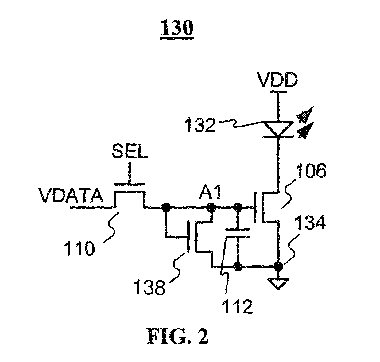
FIG. 2 illustrates another example of a pixel circuit having the drive circuit 104 of FIG. 1. The pixel circuit 130 is similar to the pixel circuit 100 of FIG. 1. The pixel circuit 130 includes an OLED 132. The OLED 132 may be same or similar to the OLED 102 of FIG. 1. In the pixel circuit 130, the drive transistor 106 is provided between one electrode (e.g., cathode electrode) of the OLED 132 and a power supply line (e.g., common ground) 134. One terminal of the discharging transistor 138 and one terminal of the storage capacitor 112 are connected to the power supply line 134. The other electrode (e.g., anode electrode) of the OLED 132 is connected to VDD.
The pixel circuit 130 provides constant averaged current over the frame time, in a manner similar to that of the pixel circuit 100 of FIG. 1.
FIG. 3 illustrates an example of method of driving a pixel circuit in accordance with an embodiment of the present invention. The waveforms of FIG. 3 are applied to a pixel circuit (e.g., 100 of FIG. 1, 130 of FIG. 2) having the drive circuit 104 of FIGS. 1 and 2.
The operation cycle of FIG. 3 includes a programming cycle 140 and a driving cycle 142. Referring to FIGS. 1 to 3, during the programming cycle 140, node A1 is charged to a programming voltage through the switch transistor 110 while the select line SEL is high. During the driving cycle 142, node A1 is discharged through the discharging transistor 108. Since the drive transistor 106 and the discharging transistor 108 have the same bias condition, they experience the same threshold voltage shift. Considering that the discharge time is a function of transconductance of the discharging transistor 108, the discharge time increases as the threshold voltage of the drive transistor 106/the discharging transistor 108 increases. Therefore, the average current of the pixel (100 of FIG. 1, 130 of FIG. 2) over the frame time remains constant. In an example, the discharging transistor is a very weak transistor with short width (W) and long channel length (L). The ratio of the width (W) to the length (L) may change based on different situations.
In addition, in the pixel circuit 130 of FIG. 2, an increase in the OLED voltage for the OLED 132 results in longer discharge time. Thus, the averaged pixel current will remain constant even after the OLED degradation.
FIG. 4 illustrates an example of a display system for the drive circuit of FIGS. 1 and 2. The display system 1000 of FIG. 4 includes a display array 1002 having a plurality of pixels 1004. The pixel 1004 includes the drive circuit 104 of FIGS. 1 and 2, and may be the pixel circuit 100 of FIG. 1 or the pixel circuit 130 of FIG. 2.
The display array 1002 is an active matrix light emitting display. In one example, the display array 1002 is an AMOLED display array. The display array 1002 may be a single color, multi-color or a fully color display, and may include one or more than one electroluminescence (EL) element (e.g., organic EL). The display array 1002 may be used in mobiles, personal digital assistants (PDAs), computer displays, or cellular phones.
Select lines SELi and SELi+1 and data lines VDATAj and VDATAj+1 are provided to the display array 1002. Each of the select lines SELi and SELi+1 corresponds to SEL of FIGS. 1 and 2. Each of the data lines VDATAj and VDATAj+1 corresponds to VDATA of FIGS. 1 and 2. The pixels 1004 are arranged in rows and columns. The select line (SELi, SELi+1) is shared between common row pixels in the display array 1002. The data line (VDATAj, VDATAj+1) is shared between common column pixels in the display array 1002.
In FIG. 4, four pixels 1004 are shown. However, the number of the pixels 1004 may vary in dependence upon the system design, and does not limited to four. In FIG. 4, two select lines and two data lines are shown. However, the number of the select lines and the data lines may vary in dependence upon the system design, and does not limited to two.
A gate driver 1006 drives SELi and SELi-1-1. The gate driver 1006 may be an address driver for providing address signals to the address lines (e.g., select lines). A data driver 1008 generates a programming data and drives VDATAj and VDATAj+1. A controller 1010 controls the drivers 1006 and 1008 to drive the pixels 1004 as described above.
FIG. 5 illustrates an example of a pixel circuit to which a pixel drive scheme in accordance with another embodiment of the present invention. The pixel circuit 160 of FIG. 5 includes an OLED 162 and a drive circuit 164 for driving the OLED 162. The drive circuit 164 includes a drive transistor 166, a discharging transistor 168, first and second switch transistors 170 and 172, and a storage capacitor 174.
The pixel circuit 160 is similar to the pixel circuit 130 of FIG. 2. The drive circuit 164 is similar to the drive circuit 104 of FIGS. 1 and 2. The transistors 166, 168 and 170 correspond to the transistors 106, 108 and 110 of FIGS. 1 and 2, respectively. The transistors 166, 168, and 170 may be same or similar to the transistors 106, 108 and 110 of FIGS. 1 and 2. The storage capacitor 174 corresponds to the storage capacitor 112 of FIGS. 1 and 2. The storage capacitor 174 may be same or similar to the storage capacitor 112 of FIGS. 1 and 2. The OLED 162 corresponds to the OLED 132 of FIG. 2. The OLED 162 may be same or similar to the OLED 132 of FIG. 2.
In one example, the switch transistor 172 is a n-type transistor. In another example, the switch transistor 172 is a p-type transistor. In one example, each of the transistors 166, 168, 170, and 172 includes a gate terminal, a source terminal and a drain terminal.
The transistors 166, 168, 170 and 172 may be fabricated using amorphous silicon, nano/micro crystalline silicon, poly silicon, organic semiconductors technologies (e.g., organic TFT), NMOS/PMOS technology or CMOS technology (e.g., MOSFET).
In the pixel circuit 160, the switch transistor 172 and the discharging transistor 168 are connected in series between the gate terminal of the drive transistor 166 and a power supply line (e.g., common ground) 176. The gate terminal of the switch transistor 172 is connected to a bias voltage line VB. The gate terminal of the discharging transistor 168 is connected to the gate terminal of the drive transistor at node AZ The drive transistor 166 is provided between one electrode (e.g., cathode electrode) of the OLED 162 and the power supply line 176. The gate terminal of the switch transistor 170 is connected to SEL. One terminal of the switch transistor 170 is connected to VDATA. The other terminal of the switch transistor 170 is connected to node A2. One terminal of the storage capacitor 174 is connected to node A2. The other terminal of the storage capacitor 174 is connected to the power supply line 176.
The pixel circuit 160 provides constant averaged current over the frame time by adjusting the gate voltage of the drive transistor 166, as described below.
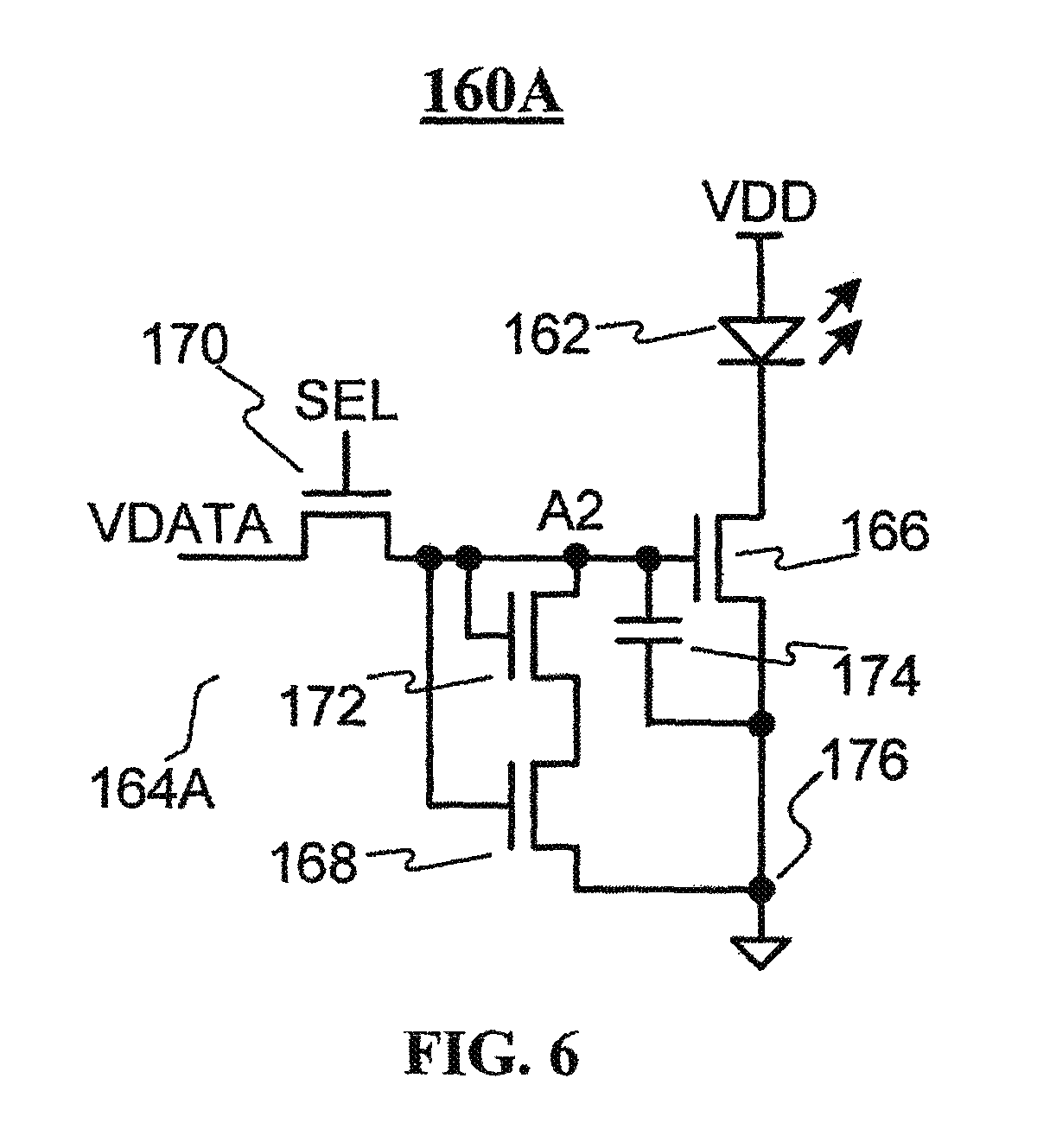
In one example, the bias voltage line VB of FIG. 5 may be shared between the pixels of the entire panel, In another example, the bias voltage VB may be connected to node A2, as shown in FIG. 6, The pixel circuit 160A of FIG. 6 includes a drive circuit 164A. The drive circuit 164A is similar to the drive circuit 164 of FIG. 5. However, in the drive circuit 164A, the gate terminal of the switch transistor 172 is connected to node A2. In a further example, the switch transistor 172 of FIG. 5 may be replaced with a resistor, as shown in FIG. 7. The pixel circuit 160B of FIG. 7 includes a drive circuit 164B. The drive circuit 164B is similar to the drive circuit 164 of FIG. 5. However, in the drive circuit 164B, a resistor 178 and the discharging transistor 168 are connected in series between node A2 and the power supply line 176.
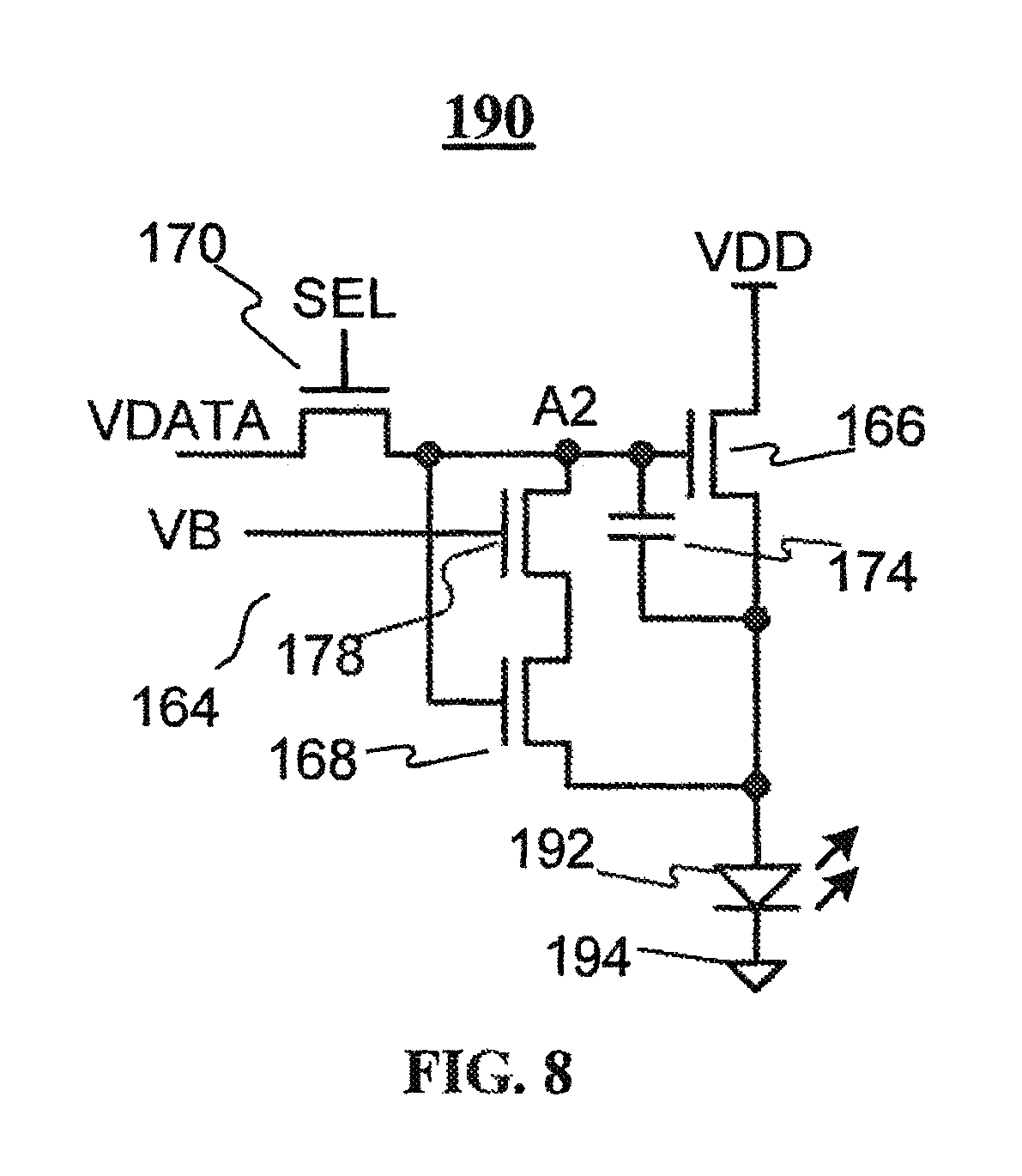
FIG. 8 illustrates another example of a pixel circuit having the drive circuit 164 of FIG. 5. The pixel circuit 190 is similar to the pixel circuit 160 of FIG. 5. The pixel circuit 190 includes an OLED 192. The OLED 192 may be same or similar to the OLED 162 of FIG. 5. In the pixel circuit 190, the drive transistor 166 is provided between one electrode (e.g., anode electrode) of the OLED 192 and VDD. One terminal of the discharging transistor 168 and one terminal of the storage capacitor 174 are connected to the OLED 192. The other electrode (e.g., cathode electrode) of the OLED 192 is connected to a power supply line (e.g., common ground) 194.
In one example, the bias voltage VB of FIG. 8 is shared between the pixels of the entire panel. In another example, the bias voltage VB of FIG. 8 is connected to node A2, as it is similar to that of FIG. 6. In a further example, the switch transistor 172 of FIG. 8 is replaced with a resistor, as it is similar to that of FIG. 7.
The pixel circuit 190 provides constant averaged current over the frame time, in a manner similar to that of the pixel circuit 160 of FIG. 5.
FIG. 9 illustrates an example of method of driving a pixel circuit in accordance with another embodiment of the present invention. The waveforms of FIG. 9 are applied to a pixel circuit (e.g., 160 of FIG. 5, 190 of FIG. 8) having the drive circuit 164 of FIGS. 5 and 8.
The operation cycle of FIG. 9 includes a programming cycle 200 and a driving cycle 202. Referring to FIGS. 5, 8 and 9, during the programming cycle 200, node A2 is charged to a programming voltage (Vp) through the switch transistor 170 while SEL is high. During the driving cycle 202, node A2 is discharged through the discharging transistor 168, Since the drive transistor 166 and the discharging transistor 168 have the same bias condition, they experience the same threshold voltage shift Considering that the discharge time is a function of transconductance of the discharging transistor 168, the discharge time increases as the threshold voltage of the drive transistor 166/the discharging transistor 168 increases, Therefore, the average current of the pixel (160 of FIG. 5, 190 of FIG. 8) over the frame time remains constant. Here, the switch transistor 172 forces the discharging transistor 168 in the linear regime of operation, and so reduces feedback gain. Therefore, the discharging transistor 168 may be a unity transistor with the minimum channel length and width. The width and length of the unity transistor are the minimum allowed by the technology.
In addition, in the pixel circuit 190 of FIG. 8, an increase in the OLED voltage for the OLED 192 results in longer discharge time. Thus, the averaged pixel current will remain constant even after the OLED degradation.
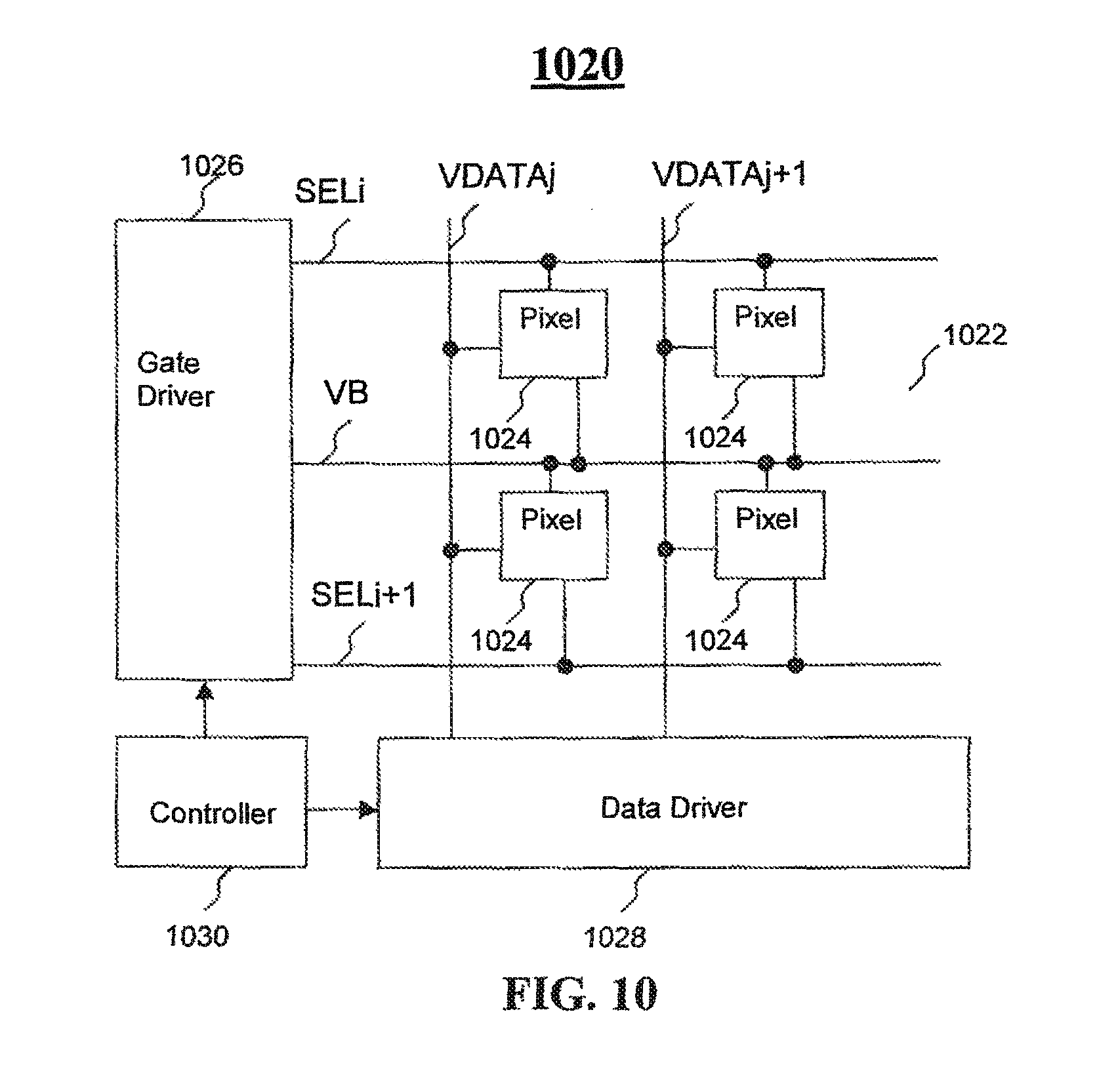
FIG. 10 illustrates an example of a display system for the drive circuit of FIGS. 5 and 8. The display system 1020 of FIG. 10 includes a display array 1022 having a plurality of pixels 1024. The pixel 1024 includes the drive circuit 164 of FIGS. 5 and 8, and may be the pixel circuit 130 of FIG. 5 or the pixel circuit 190 of FIG. 8.
The display array 1022 is an active matrix light emitting display. In one example, the display array 1022 is an AMOLED display array. The display array 1022 may be a single color, multi-color or a fully color display, and may include one or more than one EL element (e.g., organic EL). The display array 1022 may be used in mobiles, PDAs, computer displays, or cellular phones,
Each of select lines SELi and SELi+1 corresponds to SEL of FIGS. 5 and 8. VB corresponds to VB of FIGS. 5 and 8. Each of data lines VDATAj and VDATAj+1 corresponds to VDATA of FIGS. 5 and 8. The pixels 1024 are arranged in rows and columns. The select line (SELi, SEL1+1) is shared between common row pixels in the display array 1022. The data line (VDATAj, VDATAj+1) is shared between common column pixels in the display array 1022. The bias voltage line VB is shared by the ith and (i+1)th rows. In another--example, the VB may be shared by the entire array 1022.
In FIG. 10, four pixels 1024 are shown. However, the number of the pixels 1024 may vary in dependence upon the system design, and does not limited to four. In FIG. 10, two select lines and two data lines are shown. However, the number of the select lines and the data lines may vary in dependence upon the system design, and does not limited to two.
A gate driver 1026 drives SELi and SELi+1, and VB, The gate driver 1026 may include an address driver for providing address signals to the display array 1022. A data driver 1028 generates a programming data and drives VDATAj and VDATAj+1, A controller 1030 controls the drivers 1026 and 1028 to drive the pixels 1024 as described above.
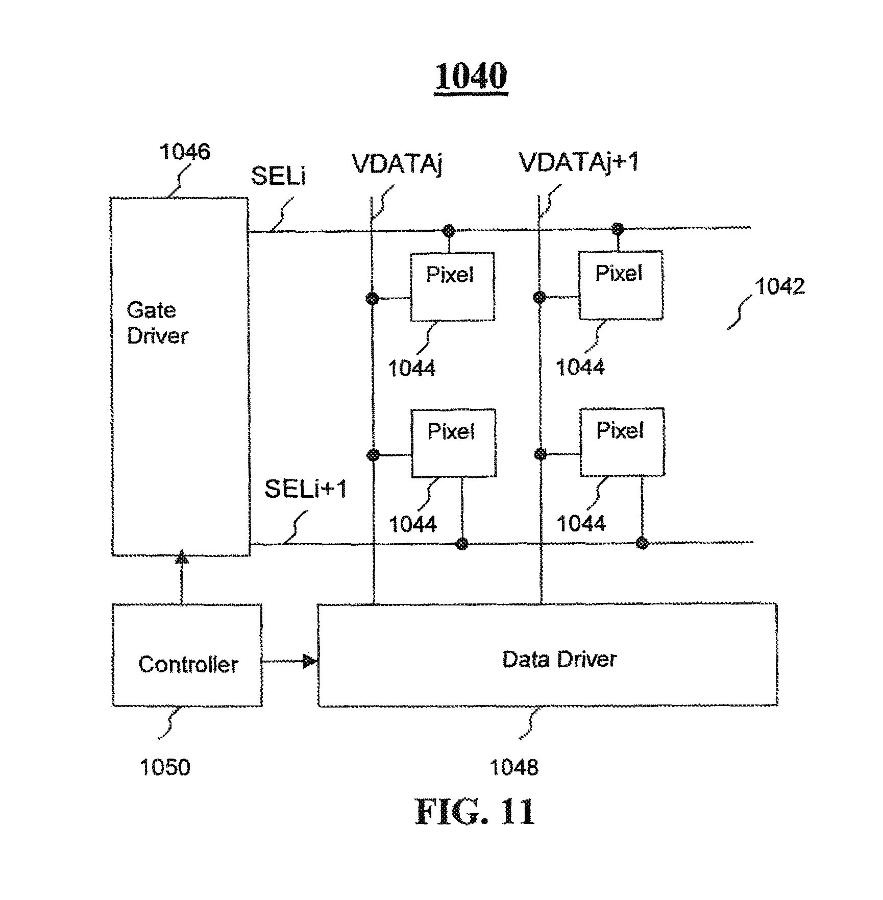
FIG. 11 illustrates an example of a display system for the drive circuit of FIGS. 6 and 7. The display system 1040 of FIG. 11 includes a display array 1042 having a plurality of pixels 1044. The pixel 1044 includes the drive circuit 164A of FIG. 6 or 164B of FIG. 7, and may be the pixel circuit 160A of FIG. 6 or the pixel circuit 160B of FIG. 7.
The display array 1042 is an active matrix light emitting display, In one example, the display array 1042 is an AMOLED display array, The display array 1042 may be a single color, multi-color or a fully color display, and may include one or more than one EL element (e.g., organic EL). The display array 1042 may be used in mobiles, PDAs, computer displays, or cellular phones.
Each of select lines SELi and SELi+1 corresponds to SEL of FIGS. 6 and 7. Each of data lines VDATAj and VX)ATAj+1 corresponds to VDATA of FIGS. 6 and 7. The pixels 1044 are arranged in rows and columns The select line (SELL, SELi+1) is shared between common row pixels in the display array 1042, The data line (VDATAj, VDATAj+1) is shared between common column pixels in the display array 1042.
In FIG. 11, four pixels 1044 are shown. However, the number of the pixels 1044 may vary in dependence upon the system design, and does not limited to four. In FIG. 11, two select lines and two data lines are shown, However, the number of the select lines and the data lines may vary in dependence upon the system design, and does not limited to two.
A gate driver 1046 drives SELi and SELi.+-.1. The gate driver 1046 may be an address driver for providing address signals to the address lines (e.g., select lines). A data driver 1048 generates a programming data and drives VDATAj and VDATAj+1, A controller 1040 controls the drivers 1046 and 1048 to drive the pixels 1044 as described above.
FIG. 12 illustrates simulation results for the pixel circuit 100 of FIG. 1. In FIG. 12, "g1" represents the current of the pixel circuit 100 presented in FIG. 1 for different shifts in the threshold voltage of the drive transistor 106 and initial current of 500 nA; "g2" represents the current of the pixel circuit 100 for different shifts in the threshold voltage of the drive transistor 106 and initial current of 150 nA. In FIG. 12, "g3" represents the current of a conventional 2-TFT pixel circuit for different shifts in the threshold voltage of a drive transistor and initial current of 500 nA; "g4" represents the current of the conventional 2-TFT pixel circuit for different shifts in the threshold voltage of a drive transistor and initial current of 150 nA. It is obvious that the averaged pixel current is stable for the new driving scheme whereas it drops dramatically if the discharging transistor (e.g., 106 of FIG. 1) is removed from the pixel circuit (conventional 2-TFT pixel circuit).
FIG. 13 illustrates an example of a pixel circuit to which a pixel drive scheme in accordance with a further embodiment of the present invention. The pixel circuit 210 of FIG. 13 includes an OLED 212 and a drive circuit 214 for driving the OLED 212. The drive circuit 214 includes a drive transistor 216, a discharging transistor 218, first and second switch transistors 220 and 222, and a storage capacitor 224.
The pixel circuit 210 is similar to the pixel circuit 190 of FIG. 8. The drive circuit 214 is similar to the drive circuit 164 of FIGS. 5 and 8, The transistors 216, 218 and 220 correspond to the transistors 166, 168 and 170 of FIGS. 5 and 8, respectively. The transistors 216, 218, and 220 may be same or similar to the transistors 166, 168, and 170 of FIGS. 5 and 8. The transistor 222 may be same or similar to the transistor 172 of FIG. 5 or the transistor 178 of FIG. 8. In one example, each of the transistors 216, 218, 220, and 222 includes a gate terminal, a source terminal and a drain terminal, The storage capacitor 224 corresponds to the storage capacitor 174 of FIGS. 5 to 8. The storage capacitor 224 may be same or similar to the storage capacitor 174 of FIGS. 5 to 8, The OLED 212 corresponds to the OLED 192 of FIG. 8. The OLED 212 may be same or similar to the OLED 192 of FIG. 8.
The transistors 216, 218, 220, and 222 may be fabricated using amorphous silicon, nano/micro crystalline silicon, poly silicon, organic semiconductors technologies (e.g., organic TF1), NMOS/PMOS technology or CMOS technology (e.g., MOSFET).
In the pixel circuit 210, the drive transistor 216 is provided between VDD and one electrode (e.g., anode electrode) of the OLED 212. The switch transistor 222 and the discharging transistor 218 are connected in series between the gate terminal of the drive transistor 216 and the OLED 212. One terminal of the switch transistor 222 is connected to the gate terminal of the drive transistor at node A3. The gate terminal of the discharging transistor 218 is connected to node M. The storage capacitor 224 is provided between node A3 and the OLED 212. The switch transistor 220 is provided between VDATA and node A3. The gate terminal of the switch transistor 220 is connected to a select line SEL[n]. The gate terminal of the switch transistor 222 is connected to a select line SEL [n+1]. The other electrode (e.g., cathode electrode) of the OLED 212 is connected to a power supply line (e.g., common ground) 226. In one example, SEL [n] is the address line of the nth row in a display array, and SEL[n+1] is the address line of the (n+1)th row in the display array.
The pixel circuit 210 provides constant averaged current over the frame time by adjusting the gate voltage of the drive transistor 216, as described below.
FIG. 14 illustrates another example of a pixel circuit having the drive circuit 214 of FIG. 13. The pixel circuit 240 of FIG. 14 is similar to the pixel circuit 160 of FIG. 5. The pixel circuit 240 includes an OLED 242. The OLED 242 may be same or similar to the OLED 162 of FIG. 5, Tn the pixel circuit 240, the drive transistor 216 is provided between one electrode (e.g., cathode electrode) of the OLED 242 and a power supply line (e.g., common ground) 246. One terminal of the discharging transistor 218 and one terminal of the storage capacitor 224 are connected to the power supply line 246. The other electrode (e.g., anode electrode) of the OLED 242 is connected to VDD. The gate terminal of the switch transistor 220 is connected to the select line SEL[n]. The gate terminal of the switch transistor 222 is connected to the select line SEL [n+1].
The pixel circuit 240 provides constant averaged current over the frame time, in a manner similar to that of the pixel circuit 210 of FIG. 13.
FIG. 15 illustrates an example of method of driving a pixel circuit in accordance with an embodiment of the present invention. The waveforms of FIG. 15 are applied to a pixel circuit (e.g., 210 of FIG. 13, 240 of FIG. 14) having the drive circuit 214 of FIGS. 13 and 14.
The operation cycles of FIG. 15 include three operation cycles 250, 252 and 254. The operation cycle 250 forms a programming cycle, the operation cycle 252 forms a compensation cycle, and the operation cycle 254 forms a driving cycle. Referring to FIGS. 13 to 15, during the programming cycle 250, node A3 is charged to a programming voltage through the switch transistor 220 while SEL[n] is high. During the second operating cycle 252 SEL[n+1] goes to a high voltage. SEL[n] is disenabled (or deactivated). Node A3 is discharged through the discharging transistor 218, During the third operating cycle 254, SEL[n] and SEL[n+1] are disenabled. Since the drive transistor 216 and the discharging transistor 218 have the same bias condition, they experience the same threshold voltage shift. Considering that the discharge time is a function of transconductance of the discharging transistor 218, the discharged voltage decreases as the threshold voltage of the drive transistor 216/the discharging transistor 218 increases. Therefore, the gate voltage of the drive transistor 216 is adjusted accordingly.
In addition, in the pixel 240 of FIG. 14, an increase in the OLED voltage for the OLED 242 results in higher gate voltage. Thus, the pixel current remains constant
FIG. 16 illustrates an example of a display system for the drive circuit of FIGS. 13 and 14. The display system 1060 of FIG. 16 includes a display array 1062 having a plurality of pixels 1064. The pixel 1064 includes the drive circuit 214 of FIGS. 13 and 14, and may be the pixel circuit 210 of FIG. 13 or the pixel circuit 240 of FIG. 14.
The display array 1062 is an active matrix light emitting display. In one example, the display array 1062 is an AMOLED display array. The display array 1062 may be a single color, multi-color or a fully color display, and may include one or more than one EL element (e.g., organic EL), The display array 1062 may be used in mobiles, PDAs, computer displays, or cellular phones.
SEL[k] (k=n+1, n+2) is an address line for the kth row. VDATAI (1=j, j+1) is a data line and corresponds to VDATA of FIGS. 13 and 14. The pixels 1064 are arranged in rows and columns. The select line SEL[k] is shared between common row pixels in the display array 1062. The data line VDATAI is shared between common column pixels in the display array 1062.
In FIG. 16, four pixels 1064 are shown. However, the number of the pixels 1064 may vary in dependence upon the system design, and does not limited to four. In FIG. 16, three address lines and two data lines are shown. However, the number of the address lines and the data lines may vary in dependence upon the system design.
A gate driver 1066 drives SEL[k]. The gate driver 1066 may be an address driver for providing address signals to the address lines (e.g., select lines). A data driver 1068 generates a programming data and drives VDATA1. A controller 1070 controls the drivers 1066 and 1068 to drive the pixels 1064 as described above.
FIG. 17 illustrates the simulation results for the pixel circuit 160 of FIG. 5, In FIG. 17, "g5" represents the current of the pixel circuit 160 presented in FIG. 5 for different shifts in the threshold voltage of the drive transistor 166 and initial current of 630 nA; "g6" represents the current of the pixel circuit 160 for different shifts in the threshold voltage of the drive transistor 166 and initial current of 430 nA. It is seen that the pixel current is highly stable even after a 2-V shift in the threshold voltage of the drive transistor. Since the pixel circuit 210 of FIG. 13 is similar to the pixel circuit 160 of FIG. 15, it is apparent to one of ordinary skill in the art that the pixel current of the pixel circuit 210 will be also stable.
FIG. 18 illustrates the simulation results for the pixel circuit 160 of FIG. 5. In FIG. 18, "g7" represents the current of the pixel circuit 160 presented in FIG. 5 for different OLED voltages of the drive transistor 166 and initial current of 515 nA; "g8" represents the current of the pixel circuit 160 for different OLED voltages of the drive transistor 166 and initial current of 380 nA, It is seen that the pixel current is highly stable even after a 2-V shift in the voltage of the OLED. Since the pixel circuit 210 of FIG. 13 is similar to the pixel circuit 160 of FIG. 15, it is apparent to one of ordinary skill in the art that the pixel current of the pixel circuit 210 will be also stable.
FIG. 19 is a diagram showing programming and driving cycles for driving the display arrays 1062 of FIG. 16. In FIG. 16, each of ROW j (j=1, 2, 3, 4) represents the jth row of the display array 1062. In FIG. 19, "P" represents a programming cycle; "C" represents a compensation cycle; and "D" represents a driving cycle. The programming cycle P at the jth Row overlaps with the driving cycle D at the (j+1)th Row. The compensation cycle C at the jth Row overlaps with the programming cycle P at the (1+1)th Row. The driving cycle D at the jth Row overlaps with the compensation cycle C at the (j+1)th Row.
FIG. 20 illustrates an example of a pixel circuit to which a pixel drive scheme in accordance with a further embodiment of the present invention is applied. The pixel circuit 300 of FIG. 20 includes an OLED 302 and a drive circuit 304 for driving the OLED 302. The drive circuit 304 includes a drive transistor 306, a switch transistor 308, a discharging transistor 310, and a storage capacitor 312. The OLED 302 includes, for example, an anode electrode, a cathode electrode and an emission layer between the anode electrode and the cathode electrode.
In one example, the transistors 306, 308 and 310 are n-type transistors. In another example, the transistors 306, 308 and 310 are p-type transistors or a combination of n-type and p-type transistors. In one example, each of the transistors 306, 308 and 310 includes a gate terminal, a source terminal and a drain terminal. The transistors 306, 308 and 310 may be fabricated using amorphous silicon, nano/micro crystalline silicon, poly silicon, organic semiconductors technologies (e.g., organic TFT), NMOS/PMOS technology or CMOS technology (e.g., MOSFET).
The drive transistor 306 is provided between a voltage supply line Vdd and the OLED 302. One terminal (e.g., source) of the drive transistor 306 is connected to Vdd. The other terminal (e.g., drain) of the drive transistor 306 is connected to one electrode (e.g., anode electrode) of the OLED 302. The other electrode (e.g., cathode electrode) of the OLED 302 is connected to a power supply line (e.g., common ground) 314. One terminal of the storage capacitor 312 is connected to the gate terminal of the drive transistor 306 at node A4. The other terminal of the storage capacitor 312 is connected to Vdd. The gate terminal of the switch transistor 308 is connected to a select line SEL M. One terminal of the switch transistor 308 is connected to a data line VDATA. The other terminal of the switch transistor 308 is connected to node A4. The gate terminal of the discharging transistor 310 is connected to a select line SEL [i-1] or SEL[i+1]. In one example, the select line SEL[m] (m=i-1, i, 1+1) is an address line for the mth row in a display array. One terminal of the discharging transistor 310 is connected to node A4. The other terminal of the discharging transistor 310 is connected to a sensor 316. In one example, each pixel includes the sensor 316. In another example, the sensor 316 is shared by a plurality of pixel circuits.
The sensor 316 includes a sensing terminal and a bias terminal Vb1, The sensing terminal of the sensor 316 is connected to the discharging transistor 310. The bias terminal Vb1 may be connected, for example, but not limited to, ground, Vdd or the one terminal (e.g., source) of the drive transistor 306. The sensor 316 detects energy transfer from the pixel circuit. The sensor 316 has a conductance that varies in dependence upon the sensing result, The emitted light or thermal energy by the pixel absorbed by the sensor 316 and so the carrier density of the sensor changes. The sensor 316 provides feedback by, for example, but not limited to, optical, thermal or other means of transduction. The sensor 316 may be, but not limited to, an optical sensor or a thermal sensor. As described below, node A4 is discharged in dependence upon the conductance of the sensor 316.
The drive circuit 304 is used to implement programming, compensating/calibrating and driving of the pixel circuit. The pixel circuit 300 provides constant luminance over the lifetime of its display by adjusting the gate voltage of the drive transistor 306.
FIG. 21 illustrates another example of a pixel circuit having the drive circuit 304 of FIG. 20. The pixel circuit 330 of FIG. 21 is similar to the pixel circuit 300 of FIG. 20. The pixel circuit 330 includes an OLED 332. The OLED 332 may be same or similar to the OLED 302 of FIG. 20. In the pixel circuit 330, one terminal (e.g., drain) of the drive transistor 306 is connected to one electrode (e.g., cathode electrode) of the OLED 332, and the other terminal (e.g., source) of the drive transistor 306 is connected to a power supply line (e.g., common ground) 334. In addition, one terminal of the storage capacitor 312 is connected to node A4, and the other terminal of the storage capacitor 312 is connected to the power supply line 334. The pixel circuit 330 provides constant luminance over the lifetime of its display, in a manner similar to that of the pixel circuit 300 of FIG. 20.
Referring to FIGS. 20 and 21, the aging of the drive transistor 306 and the OLED 302/332 in the pixel circuit are compensated in two different ways: in-pixel compensation and of-panel calibration.
In-pixel compensation is descried in detail. FIG. 22 illustrates an example of a method of driving a pixel circuit in accordance with a further embodiment of the present invention. By applying the waveforms of FIG. 22 to a pixel having the drive circuit 304 of FIGS. 20 and 21, the in-pixel compensation is implemented.
The operation cycles of FIG. 22 include three operation cycles 340, 342 and 344. The operation cycle 340 is a programming cycle of the ith row and is a driving cycle for the (i+1)th row. The operation cycle 342 is a compensation cycle for the ith row and is a programming cycle of the (i+1)th row. The operation cycle 344 is a driving cycle for the ith row and is a compensation cycle for the (i+1)th row.] Referring to FIGS. 20 to 22, during the programming cycle 340 for the ith row of a display, node A4 of the pixel circuit in the ith row is charged to a programming voltage through the switch transistor 308 while the select line SEL[i] is high. During the programming cycle 342 for the (i+1)th row, SEL[i+1] goes high, and the voltage stored at node A4 changes based on the conductance of the sensor 316. During the driving cycle 344 of the ith row, the current of the drive transistor 306 controls the OLED luminance.
The amount of the discharged voltage at node A4 depends on the conductance of the sensor 316. The sensor 316 is controlled by the OLED luminance or temperature. Thus, the amount of the discharged voltage reduces as the pixel ages. This results in constant luminance over the lifetime of the pixel circuit.
FIG. 23 illustrates an example of a display system for the drive circuit 304 of FIGS. 20 and 21. The display system 1080 of FIG. 23 includes a display array 1082 having a plurality of pixels 1084. The pixel 1084 includes the drive circuit 304 of FIGS. 20 and 21, and may be the pixel circuit 300 of FIG. 20 or the pixel circuit 330 of FIG. 21.
The display array 1082 is an active matrix light emitting display. In one example, the display array 1082 is an AMOLED display array. The display array 1082 may be a single color, multi-color or a fully color display, and may include one or more than one electroluminescence (EL) element (e.g., organic EL). The display array 1082 may be used in mobiles, personal digital assistants (PDAs), computer displays, or cellular phones.
SEL[i] (i=m-1, m, m+1) in FIG. 23 is an address line for the ith row. VDATAn j+1) in FIG. 23 is a data line for the nth column. The address line SEL[i] correspond to the select line SEL[i] of FIGS. 20 and 21. The data line VDATAn corresponds to VDATA of FIGS. 20 and 21.
A gate driver 1086 includes an address driver for providing an address signal to each address line to drive them. A data driver 1088 generates a programming data and drives the data line. A controller 1090 controls the drivers 1086 and 1088 to drive the pixels 1084 and implement the in-pixel compensation as described above.
In FIG. 23, four pixels 1084 are shown. However, the number of the pixels 1084 may vary in dependence upon the system design, and does not limited to four. In FIG. 23, three address lines and two data lines are shown. However, the number of the select lines and the data lines may vary in dependence upon the system design.
In FIG. 23, each of the pixels 1084 includes the sensor 316 of FIGS. 20 and 21. In another example, the display array 1080 may include one or more than one reference pixel having the sensor 316, as shown in FIG. 24.
FIG. 24 illustrates another example of a display system for the drive circuit 304 of FIGS. 20 and 21. The display system 1100 of FIG. 24 includes a display array 1102 having a plurality of pixels 1104 and one or more than one reference pixels 1106. The reference pixel 1106 includes the drive circuit 304 of FIGS. 20 and 21, and may be the pixel circuit 300 of FIG. 20 or the pixel circuit 330 of FIG. 21. In FIG. 24, two reference pixels 1106 are shown. However, the number of the pixels 1084 may vary in dependence upon the system design, and does not limited to two. The pixel 1104 includes an OLED and a drive transistor for driving the OLED, and does not include the sensor 316 of FIGS. 20 and 21. SEL_REF is a select line for selecting the discharging transistors in the array of the reference pixels 1106.
A gate driver 1108 drives the address lines and the select line SEL_REF. The gate driver 1108 may be same or similar to the gate driver 1108 of FIG. 24. A data driver 1110 drives the data lines. The data driver 1110 may be same or similar to the data driver 1088 of FIG. 23. A controller 1112 controls the drivers 1108 and 1110.
The reference pixels of FIGS. 23 and 24 (1084 of FIG. 23, 1106 of FIG. 24) may be operated to provide aging knowledge for an of-panel algorithm in which the programming voltage is calibrated at the controller (1090 of FIG. 23, 1112 of FIG. 24) or driver side (1088 of FIG. 23, 1110 of FIG. 24) as described below.
Of-panel calibration is descried in detail. Referring to FIG. 21, the of-panel calibration is implemented by extracting the aging of the pixel circuit by reading back the sensor 316, and calibrating the programming voltage. The of-panel calibration compensates for the pixel aging including the threshold Vt shift and OLED degradation.
FIG. 25 illustrates an example of a pixel system in accordance with an embodiment of the present invention. The pixel system of FIG. 25 includes a read back circuit 360. The read back circuit 360 includes a charge-pump amplifier 362 and a capacitor 364. One terminal of the charge-pump amplifier 362 is connectable to the data line VDATA via a switch SW1. The other terminal of the charge-pump amplifier 362 is connected to a bias voltage Vb2. The charge-pump amplifier 362 reads back the voltage discharged from the node A4 via the switch SW1.
The output 366 of the charge pump amplifier 362 varies in dependent upon the voltage at node A4. The time depending characteristics of the pixel circuit is readable from node A4 via the charge-pump amplifier 362.
In FIG. 25, one read back circuit 360 and one switch SW1 are illustrated for one pixel circuit. However, the read back circuit 360 and the switch SW1 may be provided for a group of pixel circuits (e,g., pixel circuits in a column). In FIG. 25, the read back circuit 360 and the switch SW1 are provided to the pixel circuit 300. In another example, the read back circuit 360 and the switch SW1 are applied to the pixel circuit 330 of FIG. 21.
FIG. 26 illustrates an example of a display system having the read back circuit 360 of FIG. 25. The display system 1120 of FIG. 26 includes a display array 1122 having a plurality of pixels 1124. The pixel 1124 includes the drive circuit 304 of FIGS. 20 and 21, and may be the pixel circuit 300 of FIG. 20 or the pixel circuit 330 of FIG. 21. The pixel 1124 may be same or similar to the pixel 1084 of FIG. 23 or 1106 of FIG. 24.
In FIG. 26, four pixels 1124 are shown. However, the number of the pixels 1124 may vary in dependence upon the system design, and does not limited to four. In FIG. 26, three address lines and two data lines are shown. However, the number of the select lines and the data lines may vary in dependence upon the system design.
For each column, a read back circuit RB1[n] (n=j, j+1) and a switch SW1[n] (not shown) are provided. The read back circuit RB 1 [n] may include the SW1 [n], The read back circuit RB1[n] and the switch SW1[n] correspond to the read back 360 and the switch SW1 of FIG. 25, respectively. In the description below, the terms RB1 and RB 1 [n] may be used interchangeably, and RB1 may refer to the read back circuit 360 of FIG. 25 for a certain row.
The display array 1122 is an active matrix light emitting display. In one example, the display array 1122 is an AMOLED display array. The display array 1122 may be a single color, multi-color or a fully color display, and may include one or more than one electroluminescence (EL) element (e.g., organic EL). The display array 1122 may be used in mobiles, personal digital assistants (PDAs), computer displays, or cellular phones.
A gate driver 1126 includes an address driver for driving the address lines. The gate driver 1126 may be same or similar to the gate driver 1086 of FIG. 23 or the gate driver 1108 of FIG. 24. A data driver 1128 generates a programming data and drives the data lines. The data driver 1128 includes a circuit for calculating the programming data based on the output of the corresponding read back circuit RB1 [n]. A controller 1130 controls the drivers 1126 and 1128 to drive the pixels 1124 as described above. The controller 1130 controls the switch SW1[n] to turn on or off so that the RB1[n] is connected to the corresponding data line VDATAn.
The pixels 1124 are operated to provide aging knowledge for the of-panel algorithm in which the programming voltage is calibrated at the controller 1130 or driver side 1128 according to the output voltage of the read back circuit RBI. A simple calibration can be scaling in which the programming voltage is scaled up by the change in the output voltage of the read back circuit RB1.
In FIG. 26, each of the pixels 1124 includes the sensor 316 of FIGS. 20 and 21. In another example, the display array 1120 may include one or more than one reference pixel having the sensor 316, as shown in FIG. 27.
FIG. 27 illustrates another example of a display system having the read back circuit of FIG. 25. The display system 1140 of FIG. 27 includes a display array 1142 having a plurality of pixels 1144 and one or more than one reference pixels 1146. The reference pixel 1146 includes the drive circuit 304 of FIGS. 20 and 21, and may be the pixel circuit 300 of FIG. 20 or the pixel circuit 330 of FIG. 21. In FIG. 27, two reference pixels 1146 are shown. However, the number of the pixels 1084 may vary in dependence upon the system design, and does not limited to two. The pixel 1144 includes an OLED and a drive transistor for driving the OLED, and does not include the sensor 316 of FIGS. 20 and 21. SEL_REF is a select line for selecting the discharging transistors in the array of the reference pixels 1146.
A gate driver 1148 drives the address lines and the select line SEL_REF. The gate driver 1148 may be same or similar to the gate driver 1126 of FIG. 26. A data driver 1150 generates a programming data, calibrates the programming data and drives the data lines. The data driver 1150 may be same or similar to the data driver 1128 of FIG. 26. A controller 1152 controls the drivers 1148 and 1150.
The reference pixels 1146 are operated to provide aging knowledge for the of-panel algorithm in which the programming voltage is calibrated at the controller 1152 or driver side 1150 according to the output voltage of the read back circuit RB1. A simple calibration can be scaling in which the programming voltage is scaled up by the change in the output voltage of the read back circuit RB1.
FIG. 28 illustrates an example of a method of driving a pixel circuit in accordance with a further embodiment of the present invention. The display system 1120 of FIG. 26 and the display system 1140 of FIG. 27 are capable of operating according to the waveforms of FIG. 28. By applying the waveforms of FIG. 28 to the display system having the read back circuit (e.g., 360 of FIG. 3, RB1 of FIGS. 26 and 27), the of-panel calibration is implemented.
The operation cycles of FIG. 28 include operation cycles 380, 382, 383, 384, and 386. The operation cycle 380 is a programming cycle for the ith row. The operation cycle 382 is a driving cycle for the ith row. The driving cycle of each row is independent of the other rows, The operation cycle-383 is an initialization cycle for the ith row. The operation cycle 384 is an integration cycle for the ith row, The operation cycle 386 is a read back cycle for the ith row.
Referring to FIGS. 25 to 28, during the programming cycle 380 for the ith row, node A4 of the pixel circuit in the ith row is charged to a programming voltage through the switch transistor 308 while the select line SEL[i] is high. During the programming cycle 380 for the ith row, node A4 is charged to a calibrated programming voltage. During the driving cycle 382 for the ith row, the OLED luminance is controlled by the driver transistor 306: During the initialization cycle 383 for the ith row, node A4 is charged to a bias voltage. During the integration cycle 384 for the ith row, the SEL[i-1] is high and so the voltage at node A4 is discharged through the sensor 316. During the read back cycle 386, the change in the voltage at node A4 is read back to be used for calibration (e.g. scaling the programming voltage).
At the beginning of the read back cycle 384, the switch SW1 of the read back circuit RB1 is on, and the data line VDATA is charged to Vb2. Also the capacitor 364 is charged to a voltage, Vpre, as a result of leakage contributed from all the pixels connected to the date line VDATA. Then the select line SEL[i] goes high and so the discharged voltage Vdisch is developed across the capacitor 364. The difference between the two extracted voltages (Vpre and Vdisch) are used to calculate the pixel aging.
The sensor 316 can be OFF most of the time and be ON just for the integration cycle 384. Thus, the sensor 316 ages very slightly. In addition, the sensor 316 can be biased correctly to suppress its degradation significantly.
In addition, this method can be used for extracting the aging of the sensor 316. FIG. 29 illustrates an example of a method of extracting the aging of the sensor 316. The extracted voltages of the sensors for a dark pixel and a dark reference pixel can be used to find out the aging of the sensor 316. For example, the display system 1140 of FIG. 27 is capable of operating according to the waveforms of FIG. 29.
The operation cycles of FIG. 29 include operation cycles 380, 382, 383, 384, and 386. The operation cycle 380 is a programming cycle for the ith row. The operation cycle 382 is a driving cycle for the ith row. The operation cycle 383 is an initialization cycle for the ith row. The operation cycle 384 is an integration cycle for the ith row. The operation cycle 386 is a read back cycle for the ith row. The operation cycle 380 (the second occurrence) is an initialization for a reference row. The operation cycle 384 (the second occurrence) is an integration cycle for the reference row. The operation cycle 386 (the second occurrence) is a read back cycle (extraction) for the reference row.
The reference row includes one or more reference pixels (e.g., 1146 of FIG. 27), and is located in the (m-1)th row. SEL_REF is a select line for selecting the discharging transistors (e.g., 310 of FIG. 25) in the reference pixels in the reference row.
Referring to FIGS. 25, 27 and 29, to extract the aging of the sensor 316, a normal pixel circuit (e.g., 1144) is OFF. The difference between the extracted voltage via the output 316 from the normal pixel and voltage extracted for the OFF state of the reference pixel (e.g., 1146) is extracted. The voltage for the OFF state of the reference pixel is extracted where the reference pixel is not under stress. This difference results in the extraction of the degradation of the sensor 316.
FIG. 30 illustrates an example of a pixel system in accordance with another embodiment of the present invention. The pixel system of FIG. 30 includes a read back circuit 400. The read-back circuit 400 includes a trans-resistance amplifier 402. One terminal of the trans-resistance amplifier 402 is connectable to the data line VDATA via a switch SW2. The trans-resistance amplifier 402 reads back the voltage discharged from the node A4 via the switch SW2. The switch SW2 may be same or similar to the switch SW1 of FIG. 25.
The output of the trans-resistance amplifier 402 varies in dependent upon the voltage at node A4. The time depending characteristics of the pixel circuit is readable from node A4 via the trans-resistance amplifier 402.
In FIG. 30, one read back circuit 400 and one switch SW2 are illustrated for one pixel circuit. However, the read back circuit 400 and the switch SW2 may be provided for a group of pixel circuits (e.g., pixel circuits in a column). In FIG. 30, the read back circuit 400 and the switch SW2 are provided to the pixel circuit 300. In another example, the read back circuit 400 and the switch SW2 are applied to the pixel circuit 330 of FIG. 21.
FIG. 31 illustrates an example of a display system having the read back circuit 400 of FIG. 30. The display system 1160 of FIG. 31 includes a display array 1162 having a plurality of pixels 1164. The pixel 1164 includes the drive circuit 304 of FIGS. 20 and 21, and may be the pixel circuit 300 of FIG. 20 or the pixel circuit 330 of FIG. 21. The pixel 1164 may be same or similar to the pixel 1124 of FIG. 26 or 1146 of FIG. 27.
In FIG. 31, four pixels 1164 are shown. However, the number of the pixels 1164 may vary in dependence upon the system design, and does not limited to four. In FIG. 31, three address lines and two data lines are shown. However, the number of the select lines and the data lines may vary in dependence upon the system design.
For each column, a read back circuit RB2[n] (n j, j+1) and a switch SW2[n] (not shown) are provided. The read back circuit RB2[n] may include the SW2[n]. The read back circuit RB2[n] and the switch SW2[n] correspond to the read back 400 and the switch SW2 of FIG. 30, respectively. In the description below, the terms RB2 and RB2[n] may be used interchangeably, and RB2 may refer to the read back circuit 400 of FIG. 30 for a certain row.
The display array 1162 is an active matrix light emitting display. In one example, the display array 1162 is an AMOLED display array. The display array 1162 may be a single color, multi-color or a fully color display, and may include one or more than one electroluminescence (EL) element (e.g., organic EL). The display array 1162 may be used in mobiles, personal digital assistants (PDAs), computer displays, or cellular phones.
A gate driver 1166 includes an address driver for driving the address lines. The gate driver 1166 may be same or similar to the gate driver 1126 of FIG. 26 or the gate driver 1148 of FIG. 27. A data driver 1168 generates a programming data and drives the data lines. The data driver 1168 includes a circuit for calculating the programming data based on the output of the corresponding read back circuit RB2[n]. A controller 1170 controls the drivers 1166 and 1168 to drive the pixels 1164 as described above. The controller 1170 controls the switch SW2[n] to turn on or off so that the RB2[n] is connected to the corresponding data line VDATAn.
The pixels 1164 are operated to provide aging knowledge for the of-panel algorithm in which the programming voltage is calibrated at the controller 1170 or driver side 1168 according to the output voltage of the read back circuit RB2. A simple calibration can be scaling in which the programming voltage is scaled up by the change in the output voltage of the read back circuit RB2.
In FIG. 31, each of the pixels 1164 includes the sensor 316 of FIGS. 20 and 21. In another example, the display array 1160 may include one or more than one reference pixel having the sensor 316, as shown in FIG. 32.
FIG. 32 illustrates another example of a display system having the read back circuit 400 of FIG. 30. The display system 1200 of FIG. 32 includes a display array 1202 having a plurality of pixels 1204 and one or more than one reference pixels 1206. The reference pixel 1206 includes the drive circuit 304 of FIGS. 20 and 21, and may be the pixel circuit 300 of FIG. 20 or the pixel circuit 330 of FIG. 21. In FIG. 32, two reference pixels 1206 are shown. However, the number of the pixels 1204. may vary in dependence upon the system design, and does not limited to two. The pixel 1204 includes an OLED and a drive transistor for driving the OLED, and does not include the sensor 316 of FIGS. 20 and 21. SEL REF is a select line for selecting the discharging transistors in the array of the reference pixels 1206.
A gate driver 1208 drives the address lines and the select line SEL REF. The gate driver 1208 may be same or similar to the gate driver 1148 of FIG. 27 or the gate driver 1166 of FIG. 31. A data driver 1210 generates a programming data, calibrates the programming data and drives the data lines. The data driver 1210 may be same or similar to the data driver 1150 of FIG. 27 or the data driver 1168 of FIG. 32. A controller 1212 controls the drivers 1208 and 1210.
The reference pixels 1206 are operated to provide aging knowledge for the of-panel algorithm in which the programming voltage is calibrated at the controller 1212 or driver side 1210 according to the output voltage of the read back circuit RB2. A simple calibration can be scaling in which the programming voltage is scaled up by the change in the output voltage of the read back circuit RB2.
FIG. 33 illustrates an example of a method of driving a pixel circuit in accordance with a further embodiment of the present invention. The display system 1160 of FIG. 31 and the display system 1200 of FIG. 32 are capable of operating according to the waveforms of FIG. 33. By applying the waveforms of FIG. 33 to the display system having the read back circuit (e.g., 400 of FIG. 30, RB2 of FIGS. 31 and 32), the of-panel calibration is implemented.
The operation cycles of FIG. 33 include operation cycles 410, 422 and 422 for a row. The operation cycle 420 is a programming cycle for the ith row. The operation cycle 422 is a driving cycle for the ith row. The operation cycle 424 is a read back (extraction) cycle for the ith row.
Referring to FIGS. 30 to 33, during the programming cycle 420 for the ith row, node A4 of the pixel circuit in the ith row is charged to a programming voltage through the switch transistor 308 while the select line SEL[i] is high. During the driving cycle 422 for the ith row, the pixel luminance is controlled by the current of the drive transistor 306. During the extraction cycle 424 for the ith row, SEL [i] and SEL[i-1] are high and the current of the sensor 316 is monitored. The change in this current is amplified by the read back circuit RB2. This change is used to measure the luminance degradation in the pixel and compensate for it by calibrating the programming voltage (e.g, scaling the programming voltage).
At the beginning of the read-back cycle 424, the switch SW2 for the row that the algorithm chooses for calibration is ON while SEL[i] is low. Therefore, the leakage current is extracted as the output voltage of the trans-resistance amplifier 402. The selection of the row can be based on stress history, random, or sequential technique. Next, SEL[i] goes high and so the sensor current related to the luminance or temperature of the pixel is read back as the output voltage of the trans-resistance amplifier 402. Using the two extracted voltages for leakage current and sensor current, one can calculated the pixel aging.
The sensor 316 can be OFF most of the time and be ON just for the operation cycle 424. Thus, the sensor 316 ages very slightly. In addition, the sensor 316 can be biased correctly to suppress its degradation significantly.
In addition, this method can be used for extracting the aging of the sensor 316. FIG. 34 illustrates an example of a method of extracting the aging of the sensor 316 of FIG. 30. For example, the display system 1200 of FIG. 32 operates according to the waveforms of FIG. 34.
The operation cycles of FIG. 34 include operation cycles 420, 422 and 424. The operation cycle 420 (the first occurrence) is a programming cycle for the ith row. The operation cycle 422 is a driving cycle for the ith row. The operation cycle 424 (the first occurrence) is a read back (extraction) cycle for the ith row. The operation cycle 424 (the second occurrence) is a read back (extraction) cycle for a reference row.
The reference row includes one or more reference pixels (e.g., 1206 of FIG. 32) and is located in the (m-1)th row. SEL REF is a select line for selecting the discharging transistors (e.g., 310 of FIG. 30) in the reference pixels in the reference row.
Referring to FIGS. 30, 32 and 34, to extract the aging of the sensor 316, a normal pixel circuit (e.g., 1204) is OFF. The difference between the extracted voltage via the output of the trans-resistance amplifier 402 from the normal pixel circuit and voltage extracted for the OFF state of the reference pixel (e.g., 1206) is extracted. The voltage for the OFF state of the reference pixel is extracted where the reference pixel is not under stress. This results in the extraction of the degradation of the sensor 316.
FIG. 35 illustrates an example of a pixel circuit to which a pixel drive scheme in accordance with a further embodiment of the present invention. The pixel circuit 500 of FIG. 35 includes an OLED 502 and a drive circuit 504 for driving the OLED 502. The drive circuit 504 includes a drive transistor 506, a switch transistor 508, a discharging transistor 510, an adjusting circuit 510, and a storage capacitor 512.
The OLED 502 may be same or similar to the OLED 212 of FIG. 13 or the OLED 302 of FIG. 20. The capacitor 512 may be same or similar to the capacitor 224 of FIG. 13 or the capacitor 312 of FIG. 20. The transistors 506, 508 and 510 may be same or similar to the transistors 206, 220, and 222 of FIG. 13 or the transistors 306, 308 and 310 of FIG. 20. In one example, each of the transistors 506, 508 and 510 includes a gate terminal, a source terminal and a drain terminal.
The drive transistor 506 is provided between a voltage supply line VDD and the OLED 502. One terminal (e.g., drain) of the drive transistor 506 is connected to VDD. The other terminal (e.g., source) of the drive transistor 506 is connected to one electrode (e.g., anode electrode) of the OLED 502. The other electrode (e.g., cathode electrode) of the OLED 502 is connected to a power supply line VSS (e.g., common ground) 514. One terminal of the storage capacitor 512 is connected to the gate terminal of the drive transistor 506 at node A5. The other terminal of the storage capacitor 512 is connected to the OLED 502. The gate terminal of the switch transistor 508 is connected to a select line SEL [n]. One terminal of the switch transistor 508 is connected to data line VDATA. The other terminal of the switch transistor 508 is connected to node A5. The gate terminal of the transistor 510 is connected to a control line CNT[n]. In one example, n represents the nth row in a display array. One terminal of the transistor 510 is connected to node A.S. The other terminal of the transistor 510 is connected to one terminal of the adjusting circuit 516. The other terminal of the adjusting circuit 516 is connected to the OLED 502.
The adjusting circuit 516 is provided to adjust the voltage of A5 with the discharging transistor 510 since its resistance changes based on the pixel aging. In one example, the adjusting circuit 516 is the transistor 218 of FIG. 13. In another example, the adjusting circuit 516 is the sensor 316 of FIG. 20.
To improve the shift in the threshold voltage of the drive transistor 506, the pixel circuit is turned off for a portion of frame time.
FIG. 36 illustrates an example of a method of driving a pixel circuit in accordance with a further embodiment of the invention. The waveforms of FIG. 36 are applied to the pixel circuit of FIG. 35. The operation cycles for the pixel circuit 500 include a programming cycle 520, a discharge cycle 522, an emission cycle 524, a reset cycle 526, and a relaxation cycle 527.
During the programming cycle 520, node A5 is charged to a programming voltage VP. During the discharge cycle 522, CNT[n] goes high, and the voltage at node A5 is discharge partially to compensate for the aging of the pixel. During the emission cycle 524, SEL[n] and CNT[n] go low. The OLED 502 is controlled by the drive transistor 506 during the emission cycle 524. During the reset cycle 526, the CNT[n] goes to a high voltage so as to discharge the voltage at node A5 completely during the reset cycle 526. During the relaxation cycle 527, the drive transistor 506 is not under stress and recovers from the emission 524. Therefore, the aging of the drive transistor 506 is reduced significantly.
FIG. 37 illustrates an example of a display system including the pixel circuit of FIG. 35. The display system 1300 of FIG. 37 includes a display array 1302 having a plurality of pixels 500. The display array 1302 is an active matrix light emitting display. In one example, the display array 1302 is an AMOLED display array. The pixels 500 are arranged in rows and columns. In FIG. 37, two pixels 500 for the nth row are shown. The display array 1302 may include more than two pixels.
The display array 1302 may be a single color, multi-color or a fully color display, and may include one or more than one electroluminescence (EL) element (e g, organic EL). The display array 1302 may be used in mobiles, personal digital assistants (PDAs), computer displays, or cellular phones.
Address line SEL[n] is proved to the nth row. Control line CNT[n] is proved to the nth row. Data line VDATAk (k=j, j+1) is proved to the kth column. The address line SEL[n] corresponds to SEL[n] of FIG. 35. The control line CNT[n] corresponds to CNT[n] of FIG. 35. The data Line VDATAk (k=j, j+1) corresponds to VDATA of FIG. 35.
A gate driver 1306 drives SEL[n]. A data driver 1308 generates a programming data and drives VDATAk. A controller 1310 controls the drivers 1306 and 1308 to drive the pixels 500 to produce the waveforms of FIG. 36.
FIG. 38 illustrates another example of a display system including the pixel circuit 500 of FIG. 35. The display system 1400 of FIG. 38 includes a display array 1402 having a plurality of pixels 500. The display array 1402 is an active matrix light emitting display. In one example, the display array 1302 is an AMOLED display array. The pixels 500 are arranged in rows and columns. In FIG. 38, four pixels 500 for the nth row are shown. The display array 1402 may include more than four pixels.
SEL[i] (i=n, n+1) is a select line and corresponds to SEL[n] of FIG. 35. CNT[i] (i=n, n+1) is a control line and corresponds to CNT[n] of FIG. 35, OUT[k] (k=n-1, n, n+1) is an output from a gate driver 1406. The select line is connectable to one of the outputs from the gate driver 1402 or VL line, VDATAm (m=j+1) is a data line and corresponds to VDATA of FIG. 35. VDATAm is controlled by a data driver 1408. A controller 1410 controls the gate driver 1406 and the data driver 1408 to operate the pixel circuit 500.
The control lines and select lines share the same output from the gate driver 1406 through switches 1412. During the discharge cycle 526 of FIG. 36, RES signal changes the switches 1412 direction and connect the select lines to the VL line which has a low voltage to turn off the transistor 508 of the pixel circuit 500. OUT[n-1] is high and so CNT[n] is high. Thus the voltage at node A5 is adjusted by the adjusting circuit 516 and discharging transistor 510. During other operation cycles, RES signal and switches 1412 connect the select lines to the corresponding output of the gate driver (e.g., SEL[n] to OUT[n]). The switches 1412 can be fabricated on the panel using the panel fabrication technology (e.g. amorphous silicon) or it can be integrated inside the gate driver.
FIG. 39 illustrates an example of a pixel circuit to which a pixel drive scheme in accordance with a further embodiment of the present invention is applied. The pixel circuit 600 is programmed according to programming information during a programming cycle, and driven to emit light according to the programming information during an emission cycle. The pixel circuit 600 of FIG. 39 includes an OLED 602 and a drive circuit 604 for driving the OLED 602. OLED 602 is a light emitting device for emitting light during an emission cycle. OLED 602 has capacitance 632. The OLED 602 includes, for example, an anode electrode, a cathode electrode and an emission layer between the anode electrode and the cathode electrode.
The drive circuit 604 includes a drive transistor 606, a switch transistor 608, a switch block 650, a storage capacitor 612 and a regulating transistor 646. The drive transistor 606 conveys a drive current through OLED 602 during the emission cycle. The storage capacitor 612 is charged with a voltage based at least in part on the programming information during the programming cycle. The switch transistor 608 is operated according to a select line SEL, and conveys the voltage to the storage capacitor 612 during the programming cycle. The regulating transistor 646 conveys a leakage current to a gate terminal of the drive transistor 606, thereby adjusting a gate voltage of the drive transistor 606.
In one example, the transistors 606, 608 and 646 are n-type transistors. In another example, the transistors 606, 608 and 646 are p-type transistors or a combination of n-type and p-type transistors. In one example, each of the transistors 606, 608 and 646 includes a gate terminal, a source terminal and a drain terminal.
The transistors 606, 608 and 646 may be fabricated using amorphous silicon, nano/micro crystalline silicon, poly silicon, organic semiconductors technologies (e.g., organic TFT), NMOS/PMOS technology or CMOS technology (e.g., MOSFET).
The drive transistor 606 is provided between a voltage supply line VDD and the OLED 602 directly or through a switch. One terminal of the drive transistor 606 is connected to VDD. The other terminal of the drive transistor 606 is connected to one electrode (e.g., anode electrode) of the OLED 602. The gate terminal of the switch transistor 608 is connected to a select line SEL. One terminal of the switch transistor 608 is connected to a data line VDATA. The other terminal of the switch transistor 608 is connected to node A. One terminal of the storage capacitor 612 is connected to node A. The other terminal of the storage capacitor 612 is connected to the OLED 602. The other electrode (e.g., cathode electrode) of the OLED 602 is connected to a power supply line (e.g., common ground) 614.
One terminal of the regulating transistor 646 is connected to the gate terminal of the drive transistor 606. The second terminal of the regulating transistor 646 is connected to one electrode (e.g., anode electrode) of the OLED 602. The gate terminal of the regulating transistor 646 is connected to the second terminal of the regulating transistor 646. Thus, regulating transistor 646 is biased in sub-threshold regime, providing very small current. At higher temperatures, the sub-threshold current of the regulating transistor 646 increases significantly, reducing the average gate voltage of the drive transistor 606.
Switch block 650 can comprise any of the configurations of discharging transistors, additional switch transistors, resistors, sensors and/or amplifiers that are described above with respect to the various embodiments of the invention. For example, as shown in FIG. 1, switch block 650 can comprise a discharging transistor 108. Discharging transistor 108 discharges the voltage charged on the storage capacitor 612 during the emission cycle. In this embodiment, one terminal of the discharging transistor 108 and its gate terminal are connected to the gate terminal of drive transistor 606 at node A. The other terminal of the discharging transistor 108 is connected to the OLED 602.
In another example, as shown in FIG. 8, switch block 650 can comprise a second switch transistor 172 and a discharging transistor 168 connected in series between the gate terminal of the drive transistor 606 and one electrode (e.g., anode electrode) of the OLED 602. The gate terminal of the switch transistor 172 is connected to a bias voltage line VB. The gate terminal of the discharging transistor 168 is connected to the gate terminal of the drive transistor 606 at node A. Discharging transistor 168 discharges the voltage charged on the storage capacitor 612 during the emission cycle.
In still another example, as shown in FIG. 13, switch block 650 can comprise a second switch transistor 222 and a discharging transistor 218 connected in series between the gate terminal of drive transistor 606 and one electrode (e.g., anode electrode) of the OLED 602. The gate terminal of the switch transistor 222 is connected to a select line SEL[n+1]. The gate terminal of the discharging transistor 218 is connected to the gate terminal of the drive transistor 606 at node A. Discharging transistor 218 discharges the voltage charged on the storage capacitor 612 during the emission cycle.
In another example, as shown in FIG. 35, switch block 650 can comprise a discharging transistor 510 connected in series between the gate terminal of drive transistor 606 and one electrode (e.g., anode electrode) of the OLED 602. The gate terminal of the discharging transistor is connected to a control line CNT[n]. The adjusting circuit 516 is provided to adjust the voltage of node A with the discharging transistor 510 since its resistance changes based on the pixel aging. In one example, the adjusting circuit 516 is the transistor 218 of FIG. 13. In another example, the adjusting circuit 516 is the sensor 316 of FIG. 20. Discharging transistor 510 discharges the voltage charged on the storage capacitor 612 during the emission cycle.
According to these embodiments, the pixel circuit 600 provides constant averaged current over the frame time.
FIG. 40 illustrates an example of a pixel circuit to which a pixel drive scheme in accordance with another embodiment of the invention is applied. The pixel circuit 610 is programmed according to programming information during a programming cycle, and driven to emit light according to the programming information during an emission cycle. The pixel circuit 610 of FIG. 40 includes an OLED 602 and a drive circuit for driving the OLED 602. OLED 602 is a light emitting device for emitting light during the emission cycle. OLED 602 has capacitance 632. The OLED 602 includes, for example, an anode electrode, a cathode electrode and an emission layer between the anode electrode and the cathode electrode.
The drive circuit includes a drive transistor 606, a first switch transistor 608, a second switch transistor 688, a storage capacitor 612, a discharging transistor 686 and a regulating transistor 646. The drive transistor 606 conveys a drive current through the OLED 602 during the emission cycle. The storage capacitor 612 is charged with a voltage based at least in part on the programming information during the programming cycle. The first switch transistor 608 is operated according to a select line and conveys the voltage to the storage capacitor 612 during the programming cycle. The discharging transistor 686 discharges the voltage on the storage capacitor 612 during the emission cycle. The regulating transistor 646 conveys a leakage current to a gate terminal of the drive transistor 606, thereby adjusting a gate voltage of the drive transistor 606.
In one example, the transistors 606, 608, 646 and 686 are n-type transistors. In another example, the transistors 606, 608, 646 and 686 are p-type transistors or a combination of n-type and p-type transistors. In one example, each of the transistors 606, 608, 646 and 686 includes a gate terminal, a source terminal and a drain terminal.
The transistors 606, 608, 646 and 686 may be fabricated using amorphous silicon, nano/micro crystalline silicon, poly silicon, organic semiconductors technologies (e.g., organic TFT), NMOS/PMOS technology or CMOS technology (e.g., MOSFET).
The drive transistor 606 is provided between a voltage supply line VDD and the OLED 602 directly or through a switch. One terminal of the drive transistor 606 is connected to VDD. The other terminal of the drive transistor 606 is connected to one electrode (e.g., anode electrode) of the OLED 602. The gate terminal of the first switch transistor 608 is connected to a select line SEL. One terminal of the switch transistor 608 is connected to a data line VDATA. The other terminal of the switch transistor 608 is connected to node A. One terminal of the storage capacitor 612 is connected to node A. The other terminal of the storage capacitor 612 is connected to the OLED 602 at node B. The other electrode (e.g., cathode electrode) of the OLED 602 is connected to a power supply line (e.g., common ground).
The gate terminal of the discharging transistor 686 is connected to a control line CNT. The control line CNT may correspond to CNT[n] of FIG. 35. One terminal of the discharging transistor 686 is connected to node A. One terminal of the second switch transistor 688 is connected to node A. The other terminal of the discharging transistor 686 is connected to the other terminal of the second switch transistor 688 at node C. The gate terminal of the second switch transistor 688 is connected to node C.
One terminal of the regulating transistor 646 is connected to node C. The second terminal of the regulating transistor 646 is connected to one electrode (e.g., anode electrode) of the OLED 602. The gate terminal of the regulating transistor is connected to node A. Thus, regulating transistor 646 is biased in sub-threshold regime, providing very small current. However, over the frame time, this small current is enough to change the gate voltage of the drive transistor 606. At higher temperatures, the sub-threshold current of the regulating transistor 646 increases significantly, reducing the average gate voltage of the drive transistor 606.
According to this embodiment, the pixel circuit 610 provides constant averaged current over the frame time.
FIG. 41 illustrates an example of a pixel circuit to which a pixel drive scheme in accordance with a further embodiment of the invention is applied. The pixel circuit 620 is programmed according to programming information during a programming cycle, and driven to emit light according to the programming information during an emission cycle. The pixel circuit 620 of FIG. 41 includes an OLED 602 and a drive circuit for driving the OLED 602. OLED 602 is a light emitting device for emitting light during the emission cycle. OLED 602 has capacitance 632. The OLED 602 includes, for example, an anode electrode, a cathode electrode and an emission layer between the anode electrode and the cathode electrode.
The drive circuit includes a drive transistor 606, a first switch transistor 608, a second switch transistor 688, a storage capacitor 612, a discharging transistor 686 and a regulating transistor 646. The drive transistor 606 conveys a drive current through the OLED 602 during the emission cycle. The storage capacitor 612 is charged with a voltage based at least in part on the programming information during the programming cycle. The first switch transistor 608 is operated according to a select line and conveys the voltage to the storage capacitor 612 during the programming cycle. The discharging transistor 686 discharges the voltage on the storage capacitor 612 during the emission cycle. The regulating transistor 646 conveys a leakage current to a gate terminal of the drive transistor 606, thereby adjusting a gate voltage of the drive transistor 606.
The drive transistor 606 is provided between a voltage supply line VDD and the OLED 602 directly or through a switch. One terminal of the drive transistor 606 is connected to VDD. The other terminal of the drive transistor 606 is connected to one electrode (e.g., anode electrode) of the OLED 602. The gate terminal of the first switch transistor 608 is connected to a select line SEL. One terminal of the switch transistor 608 is connected to a data line VDATA. The other terminal of the switch transistor 608 is connected to node A. One terminal of the storage capacitor 612 is connected to node A. The other terminal of the storage capacitor 612 is connected to the OLED 602. The other electrode (e.g., cathode electrode) of the OLED 602 is connected to a power supply line (e.g., common ground).
The gate terminal of the discharging transistor 686 is connected to a control line CNT. The control line CNT may correspond to CNT[n] of FIG. 35 or control line CNT of FIG. 40. One terminal of the second switch transistor 688 is connected to node A. The other terminal of the second switch transistor 688 is connected to the OLED 602 at node B. The gate terminal of the second switch transistor is connected to the OLED 602 at node B.
One terminal of the discharging transistor 686 is connected to node A. The other terminal of the discharging transistor 686 is connected to one terminal of the regulating transistor 646. The other terminal of the regulating transistor 646 is connected to one electrode (e.g., anode electrode) of the OLED 602 at node B. The gate terminal of the regulating transistor is connected to node A. Thus, regulating transistor 646 is biased in sub-threshold regime, providing very small current. However, over the frame time, this small current is enough to change the gate voltage of the drive transistor 606. At higher temperatures, the sub-threshold current of the regulating transistor 646 increases significantly, reducing the average gate voltage of the drive transistor 606.
According to this embodiment, the pixel circuit 610 provides constant averaged current over the frame time.
According to another embodiment, a method of operating a display having a pixel circuit 600, 610 or 620 for driving a light emitting device is provided. The method comprises charging the pixel circuit, during a programming cycle, by turning on a first switch transistor, such that a voltage is charged on a node of the pixel circuit coupled to a capacitor and a gate terminal of a drive transistor; conveying a leakage current by a regulating transistor to the gate terminal of the drive transistor, thereby adjusting the voltage at the node; and discharging the voltage at the node through a discharging transistor, during an emission cycle, during which the pixel circuit is driven to emit light according to programming information.
According to the embodiments of the present invention, the drive circuit and the waveforms applied to the drive circuit provide a stable AMOLED display despite the instability of backplane and OLED. The drive circuit and its waveforms reduce the effects of differential aging of the pixel circuits. The pixel scheme in the embodiments does not require any additional driving cycle or driving circuitry, resulting in a row cost application for portable devices including mobiles and PDAs. Also it is insensitive to the temperature change and mechanical stress, as it would be appreciated by one of ordinary skill in the art.
One or more currently preferred embodiments have been described by way of examples as described above. It will be apparent to persons skilled in the art that a number of variations and modifications can be made without departing from the scope of the invention as defined in the claims.
* * * * *
D00000
D00001
D00002
D00003
D00004
D00005
D00006
D00007
D00008
D00009
D00010
D00011
D00012
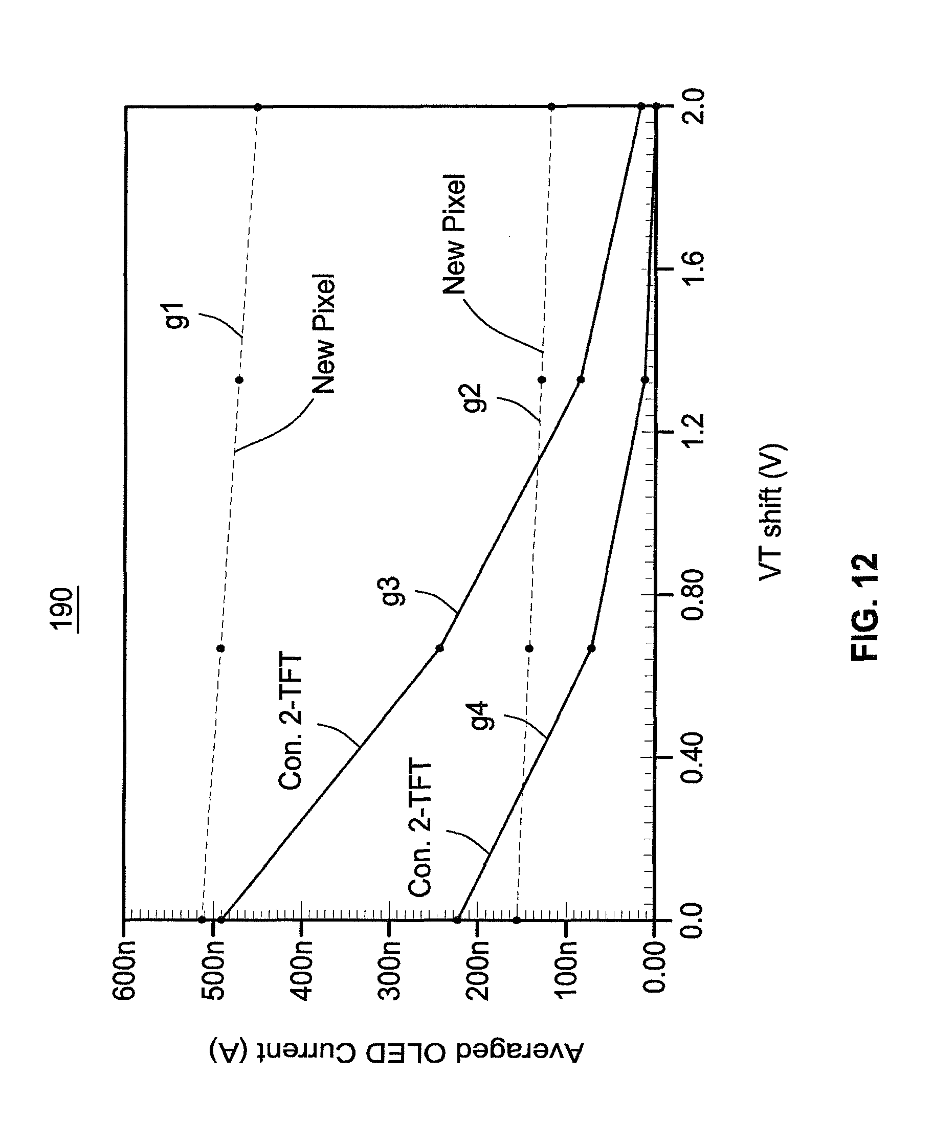
D00013

D00014

D00015

D00016

D00017
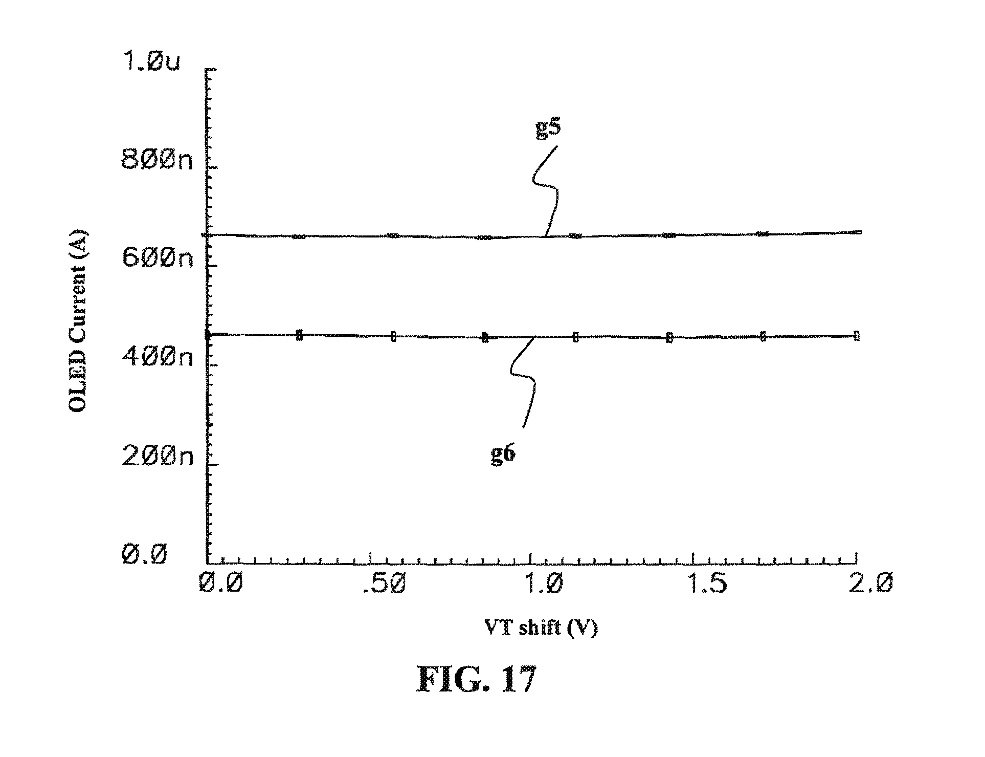
D00018

D00019

D00020

D00021

D00022

D00023
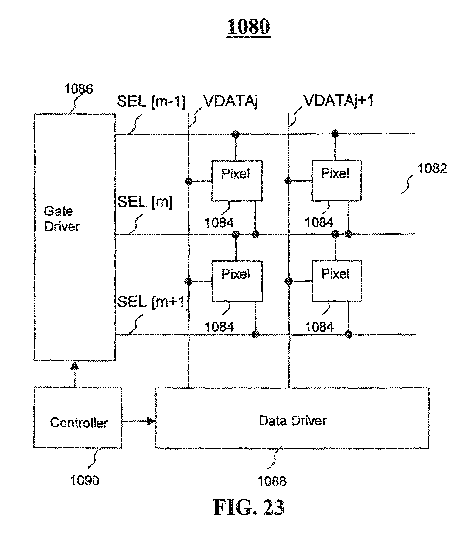
D00024

D00025

D00026

D00027

D00028

D00029

D00030

D00031
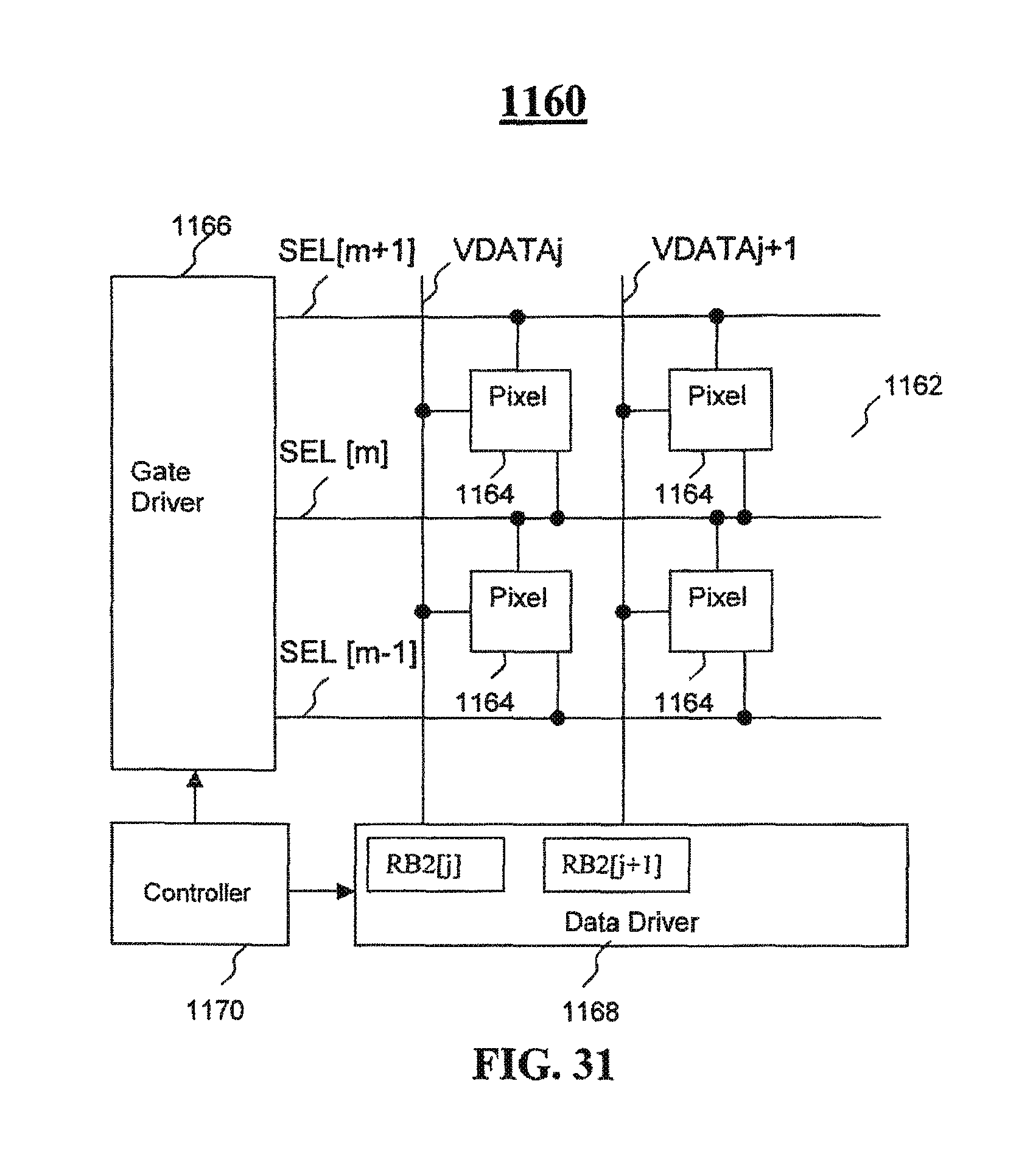
D00032

D00033

D00034

D00035

D00036

D00037

D00038
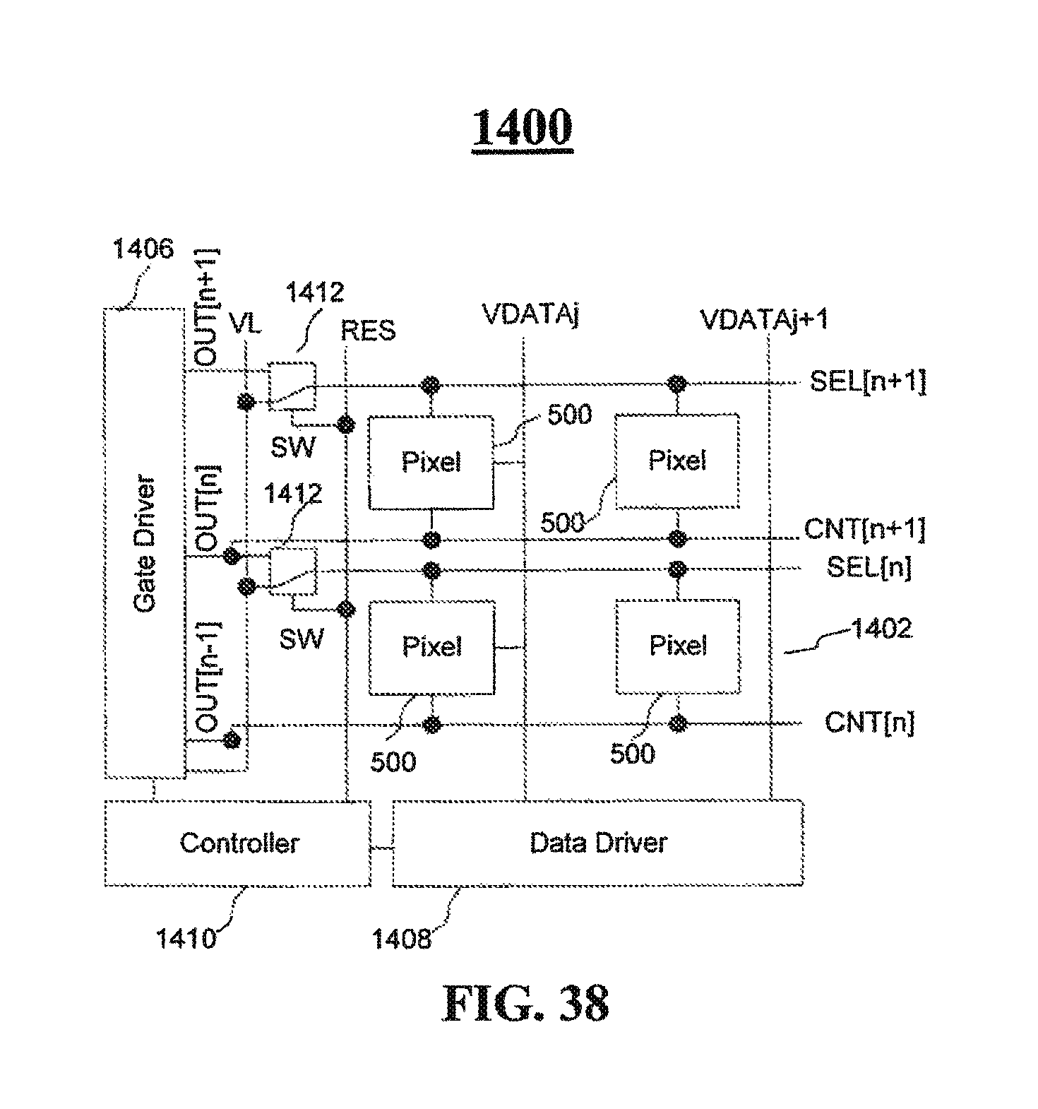
D00039

D00040

D00041

XML
uspto.report is an independent third-party trademark research tool that is not affiliated, endorsed, or sponsored by the United States Patent and Trademark Office (USPTO) or any other governmental organization. The information provided by uspto.report is based on publicly available data at the time of writing and is intended for informational purposes only.
While we strive to provide accurate and up-to-date information, we do not guarantee the accuracy, completeness, reliability, or suitability of the information displayed on this site. The use of this site is at your own risk. Any reliance you place on such information is therefore strictly at your own risk.
All official trademark data, including owner information, should be verified by visiting the official USPTO website at www.uspto.gov. This site is not intended to replace professional legal advice and should not be used as a substitute for consulting with a legal professional who is knowledgeable about trademark law.