Receiver chip for routing a wireless signal for wireless power charging or data reception
Hosseini , et al. Feb
U.S. patent number 10,218,207 [Application Number 15/046,255] was granted by the patent office on 2019-02-26 for receiver chip for routing a wireless signal for wireless power charging or data reception. This patent grant is currently assigned to Energous Corporation. The grantee listed for this patent is ENERGOUS CORPORATION. Invention is credited to Alister Hosseini, Michael A. Leabman.
View All Diagrams
| United States Patent | 10,218,207 |
| Hosseini , et al. | February 26, 2019 |
| **Please see images for: ( Certificate of Correction ) ** |
Receiver chip for routing a wireless signal for wireless power charging or data reception
Abstract
Disclosed is methods and devices for charging an electronic device. An exemplary method includes receiving, by an antenna of an electronic device, a wireless signal. A receiver chip is embedded in the electronic device and connected to the antenna, and the receiver chip includes a switch and rectifier circuitry. The method further includes: (i) in response to determining that the antenna is receiving power above a threshold level, routing, via the switch, the received wireless signal to the rectifier circuity, the rectifier circuitry being configured to convert the wireless signal into usable energy for charging a battery of the electronic device connected to the rectifier circuitry, and (ii) in response to determining that the antenna is not receiving power above the threshold level, routing, via the switch, the received wireless signal to the transceiver, the transceiver being configured to process the wireless signal as data.
| Inventors: | Hosseini; Alister (Long Beach, CA), Leabman; Michael A. (San Ramon, CA) | ||||||||||
|---|---|---|---|---|---|---|---|---|---|---|---|
| Applicant: |
|
||||||||||
| Assignee: | Energous Corporation (San Jose,
CA) |
||||||||||
| Family ID: | 59086858 | ||||||||||
| Appl. No.: | 15/046,255 | ||||||||||
| Filed: | February 17, 2016 |
Prior Publication Data
| Document Identifier | Publication Date | |
|---|---|---|
| US 20170187225 A1 | Jun 29, 2017 | |
Related U.S. Patent Documents
| Application Number | Filing Date | Patent Number | Issue Date | ||
|---|---|---|---|---|---|
| 62387205 | Dec 24, 2015 | ||||
| Current U.S. Class: | 1/1 |
| Current CPC Class: | H04B 5/0037 (20130101); H02J 7/027 (20130101); H04W 8/005 (20130101); H02J 7/025 (20130101); H02J 7/0027 (20130101); H02J 7/045 (20130101); H02J 50/20 (20160201); H02J 7/0042 (20130101); H02J 7/00034 (20200101) |
| Current International Class: | H02J 7/00 (20060101); H02J 7/02 (20160101); H02J 7/04 (20060101); H04W 8/00 (20090101); H04B 5/00 (20060101); H02J 50/20 (20160101) |
| Field of Search: | ;320/107-115 |
References Cited [Referenced By]
U.S. Patent Documents
| 787412 | April 1905 | Tesla |
| 3167775 | January 1965 | Guertler |
| 3434678 | May 1965 | Brown et al. |
| 3696384 | October 1972 | Lester |
| 3754269 | August 1973 | Clavin |
| 4101895 | July 1978 | Jones, Jr. |
| 4360741 | November 1982 | Fitzsimmons et al. |
| 4944036 | July 1990 | Hyatt |
| 4995010 | February 1991 | Knight |
| 5200759 | April 1993 | McGinnis |
| 5211471 | May 1993 | Rohrs |
| 5548292 | August 1996 | Hirshfield et al. |
| 5556749 | September 1996 | Mitsuhashi et al. |
| 5568088 | October 1996 | Dent et al. |
| 5646633 | July 1997 | Dahlberg |
| 5697063 | December 1997 | Kishigami et al. |
| 5712642 | January 1998 | Hulderman |
| 5936527 | August 1999 | Isaacman et al. |
| 5982139 | November 1999 | Parise |
| 6046708 | April 2000 | MacDonald, Jr. et al. |
| 6127799 | October 2000 | Krishnan |
| 6127942 | October 2000 | Welle |
| 6163296 | December 2000 | Lier et al. |
| 6289237 | September 2001 | Mickle et al. |
| 6329908 | December 2001 | Frecska |
| 6421235 | July 2002 | Ditzik |
| 6437685 | August 2002 | Hanaki |
| 6456253 | September 2002 | Rummeli et al. |
| 6476795 | November 2002 | Derocher et al. |
| 6501414 | December 2002 | Amdt et al. |
| 6583723 | June 2003 | Watanabe et al. |
| 6597897 | July 2003 | Tang |
| 6615074 | September 2003 | Mickle et al. |
| 6650376 | November 2003 | Obitsu |
| 6664920 | December 2003 | Mott et al. |
| 6798716 | September 2004 | Charych |
| 6803744 | October 2004 | Sabo |
| 6853197 | February 2005 | McFarland |
| 6856291 | February 2005 | Mickle et al. |
| 6911945 | June 2005 | Korva |
| 6960968 | November 2005 | Odendaal et al. |
| 6967462 | November 2005 | Landis |
| 6988026 | January 2006 | Breed et al. |
| 7003350 | February 2006 | Denker et al. |
| 7027311 | April 2006 | Vanderelli et al. |
| 7068234 | June 2006 | Sievenpiper |
| 7068991 | June 2006 | Parise |
| 7183748 | February 2007 | Unno et al. |
| 7191013 | March 2007 | Miranda et al. |
| 7196663 | March 2007 | Bolzer et al. |
| 7205749 | April 2007 | Hagen et al. |
| 7222356 | May 2007 | Yonezawa et al. |
| 7274334 | September 2007 | o'Riordan et al. |
| 7274336 | September 2007 | Carson |
| 7351975 | April 2008 | Brady et al. |
| 7359730 | April 2008 | Dennis et al. |
| 7392068 | June 2008 | Dayan |
| 7403803 | July 2008 | Mickle et al. |
| 7443057 | October 2008 | Nunally |
| 7451839 | November 2008 | Perlman |
| 7463201 | December 2008 | Chiang et al. |
| 7471247 | December 2008 | Saily |
| 7535195 | May 2009 | Horovitz et al. |
| 7614556 | November 2009 | Overhultz et al. |
| 7639994 | December 2009 | Greene et al. |
| 7643312 | January 2010 | Vanderelli et al. |
| 7652577 | January 2010 | Madhow et al. |
| 7679576 | March 2010 | Riedel et al. |
| 7702771 | April 2010 | Ewing et al. |
| 7786419 | August 2010 | Hyde et al. |
| 7812771 | October 2010 | Greene et al. |
| 7830312 | November 2010 | Choudhury et al. |
| 7844306 | November 2010 | Shearer et al. |
| 7868482 | January 2011 | Greene et al. |
| 7898105 | March 2011 | Greene et al. |
| 7904117 | March 2011 | Doan et al. |
| 7911386 | March 2011 | Ito et al. |
| 7925308 | April 2011 | Greene et al. |
| 7948208 | May 2011 | Partovi et al. |
| 8055003 | November 2011 | Mittleman et al. |
| 8070595 | December 2011 | Alderucci et al. |
| 8072380 | December 2011 | Crouch |
| 8092301 | January 2012 | Alderucci et al. |
| 8099140 | January 2012 | Arai |
| 8115448 | February 2012 | John |
| 8159090 | April 2012 | Greene et al. |
| 8159364 | April 2012 | Zeine |
| 8180286 | May 2012 | Yamasuge |
| 8228194 | July 2012 | Mickle |
| 8234509 | July 2012 | Gioscia et al. |
| 8264101 | September 2012 | Hyde et al. |
| 8264291 | September 2012 | Morita |
| 8276325 | October 2012 | Clifton et al. |
| 8278784 | October 2012 | Cook et al. |
| 8284101 | October 2012 | Fusco |
| 8310201 | November 2012 | Wright |
| 8338991 | December 2012 | Von Novak et al. |
| 8362745 | January 2013 | Tinaphong |
| 8380255 | February 2013 | Shearer et al. |
| 8384600 | February 2013 | Huang et al. |
| 8410953 | April 2013 | Zeine |
| 8411963 | April 2013 | Luff |
| 8432062 | April 2013 | Greene et al. |
| 8432071 | April 2013 | Huang et al. |
| 8446248 | May 2013 | Zeine |
| 8447234 | May 2013 | Cook et al. |
| 8451189 | May 2013 | Fluhler |
| 8452235 | May 2013 | Kirby et al. |
| 8457656 | June 2013 | Perkins et al. |
| 8461817 | June 2013 | Martin et al. |
| 8467733 | June 2013 | Leabman |
| 8497601 | July 2013 | Hall et al. |
| 8497658 | July 2013 | Von Novak et al. |
| 8552597 | August 2013 | Song et al. |
| 8558661 | October 2013 | Zeine |
| 8560026 | October 2013 | Chanterac |
| 8604746 | December 2013 | Lee |
| 8614643 | December 2013 | Leabman |
| 8621245 | December 2013 | Shearer et al. |
| 8626249 | January 2014 | Kuusilinna et al. |
| 8629576 | January 2014 | Levine |
| 8653966 | February 2014 | Rao et al. |
| 8674551 | March 2014 | Low et al. |
| 8686685 | April 2014 | Moshfeghi |
| 8712355 | April 2014 | Black et al. |
| 8712485 | April 2014 | Tam |
| 8718773 | May 2014 | Wills et al. |
| 8729737 | May 2014 | Schatz et al. |
| 8736228 | May 2014 | Freed et al. |
| 8760113 | June 2014 | Keating |
| 8770482 | July 2014 | Ackermann et al. |
| 8772960 | July 2014 | Yoshida |
| 8823319 | September 2014 | Von Novak, III et al. |
| 8832646 | September 2014 | Wendling |
| 8854176 | October 2014 | Zeine |
| 8860364 | October 2014 | Low et al. |
| 8897770 | November 2014 | Frolov et al. |
| 8903456 | December 2014 | Chu et al. |
| 8917057 | December 2014 | Hui |
| 8923189 | December 2014 | Leabman |
| 8928544 | January 2015 | Massie et al. |
| 8937408 | January 2015 | Ganem et al. |
| 8946940 | February 2015 | Kim et al. |
| 8963486 | February 2015 | Kirby et al. |
| 8970070 | March 2015 | Sada et al. |
| 8989053 | March 2015 | Skaaksrud et al. |
| 9000616 | April 2015 | Greene et al. |
| 9001622 | April 2015 | Perry |
| 9006934 | April 2015 | Kozakai et al. |
| 9021277 | April 2015 | Shearer et al. |
| 9030161 | May 2015 | Lu et al. |
| 9059598 | June 2015 | Kang et al. |
| 9059599 | June 2015 | Won et al. |
| 9077188 | July 2015 | Moshfeghi |
| 9083595 | July 2015 | Rakib et al. |
| 9088216 | July 2015 | Garrity et al. |
| 9124125 | September 2015 | Leabman et al. |
| 9130397 | September 2015 | Leabman et al. |
| 9130602 | September 2015 | Cook |
| 9142998 | September 2015 | Yu et al. |
| 9143000 | September 2015 | Leabman et al. |
| 9143010 | September 2015 | Urano |
| 9178389 | November 2015 | Hwang |
| 9225196 | December 2015 | Huang et al. |
| 9240469 | January 2016 | Sun et al. |
| 9242411 | January 2016 | Kritchman et al. |
| 9244500 | January 2016 | Cain et al. |
| 9252628 | February 2016 | Leabman et al. |
| 9270344 | February 2016 | Rosenberg |
| 9282582 | March 2016 | Dunsbergen et al. |
| 9294840 | March 2016 | Anderson et al. |
| 9297896 | March 2016 | Andrews |
| 9318898 | April 2016 | John |
| 9368020 | June 2016 | Bell et al. |
| 9401977 | July 2016 | Gaw |
| 9409490 | August 2016 | Kawashima |
| 9419335 | August 2016 | Pintos |
| 9438045 | September 2016 | Leabman |
| 9438046 | September 2016 | Leabman |
| 9444283 | September 2016 | Son et al. |
| 9450449 | September 2016 | Leabman et al. |
| 9461502 | October 2016 | Lee et al. |
| 9520725 | December 2016 | Masaoka et al. |
| 9520748 | December 2016 | Hyde et al. |
| 9522270 | December 2016 | Perryman et al. |
| 9537354 | January 2017 | Bell et al. |
| 9537357 | January 2017 | Leabman |
| 9537358 | January 2017 | Leabman |
| 9538382 | January 2017 | Bell et al. |
| 9544640 | January 2017 | Lau |
| 9559553 | January 2017 | Bae |
| 9564773 | February 2017 | Pogorelik et al. |
| 9571974 | February 2017 | Choi et al. |
| 9590317 | March 2017 | Zimmerman et al. |
| 9590444 | March 2017 | Walley |
| 9620996 | April 2017 | Zeine |
| 9647328 | May 2017 | Dobric |
| 9706137 | July 2017 | Scanlon et al. |
| 9711999 | July 2017 | Hietala et al. |
| 9723635 | August 2017 | Nambord et al. |
| 9793758 | October 2017 | Leabman |
| 9793764 | October 2017 | Perry |
| 9806564 | October 2017 | Leabman |
| 9819230 | November 2017 | Petras et al. |
| 9825674 | November 2017 | Leabman |
| 9853361 | December 2017 | Chen et al. |
| 9866279 | January 2018 | Bell et al. |
| 2001/0027876 | October 2001 | Tsukamoto et al. |
| 2002/0001307 | January 2002 | Nguyen et al. |
| 2002/0024471 | February 2002 | Ishitobi |
| 2002/0028655 | March 2002 | Rosener et al. |
| 2002/0034958 | March 2002 | Oberschmidt et al. |
| 2002/0054330 | May 2002 | Jinbo et al. |
| 2002/0065052 | May 2002 | Pande et al. |
| 2002/0072784 | June 2002 | Sheppard et al. |
| 2002/0095980 | July 2002 | Breed et al. |
| 2002/0103447 | August 2002 | Terry |
| 2002/0133592 | September 2002 | Matsuda |
| 2002/0172223 | November 2002 | Stilp |
| 2003/0005759 | January 2003 | Breed et al. |
| 2003/0058187 | March 2003 | Billiet et al. |
| 2003/0076274 | April 2003 | Phelan et al. |
| 2003/0179152 | September 2003 | Watada et al. |
| 2003/0179573 | September 2003 | Chun |
| 2003/0192053 | October 2003 | Sheppard et al. |
| 2004/0019624 | January 2004 | Sukegawa |
| 2004/0020100 | February 2004 | O'Brian et al. |
| 2004/0036657 | February 2004 | Forster et al. |
| 2004/0066251 | April 2004 | Eleftheriades et al. |
| 2004/0107641 | June 2004 | Walton et al. |
| 2004/0113543 | June 2004 | Daniels |
| 2004/0119675 | June 2004 | Washio et al. |
| 2004/0130425 | July 2004 | Dayan et al. |
| 2004/0130442 | July 2004 | Breed |
| 2004/0142733 | July 2004 | Parise |
| 2004/0145342 | July 2004 | Lyon |
| 2004/0196190 | October 2004 | Mendolia et al. |
| 2004/0203979 | October 2004 | Attar et al. |
| 2004/0207559 | October 2004 | Milosavljevic |
| 2004/0218759 | November 2004 | Yacobi |
| 2004/0259604 | December 2004 | Mickle et al. |
| 2004/0263124 | December 2004 | Wieck et al. |
| 2005/0007276 | January 2005 | Barrick et al. |
| 2005/0030118 | February 2005 | Wang |
| 2005/0046584 | March 2005 | Breed |
| 2005/0055316 | March 2005 | Williams |
| 2005/0077872 | April 2005 | Single |
| 2005/0093766 | May 2005 | Turner |
| 2005/0116683 | June 2005 | Cheng |
| 2005/0117660 | June 2005 | Vialle et al. |
| 2005/0134517 | June 2005 | Gottl |
| 2005/0171411 | August 2005 | Kenknight |
| 2005/0198673 | September 2005 | Kit et al. |
| 2005/0227619 | October 2005 | Lee et al. |
| 2005/0232469 | October 2005 | Schofield |
| 2005/0237249 | October 2005 | Nagel |
| 2005/0237258 | October 2005 | Abramov et al. |
| 2005/0282591 | December 2005 | Shaff |
| 2006/0013335 | January 2006 | Leabman |
| 2006/0019712 | January 2006 | Choi |
| 2006/0030279 | February 2006 | Leabman et al. |
| 2006/0033674 | February 2006 | Essig, Jr. et al. |
| 2006/0071308 | April 2006 | Tang et al. |
| 2006/0092079 | May 2006 | De Rochemont |
| 2006/0094425 | May 2006 | Mickle et al. |
| 2006/0113955 | June 2006 | Nunally |
| 2006/0119532 | June 2006 | Yun et al. |
| 2006/0136004 | June 2006 | Cowan et al. |
| 2006/0160517 | July 2006 | Yoon |
| 2006/0183473 | August 2006 | Ukon |
| 2006/0190063 | August 2006 | Kanzius |
| 2006/0192913 | August 2006 | Shutou et al. |
| 2006/0199620 | September 2006 | Greene et al. |
| 2006/0238365 | October 2006 | Vecchione et al. |
| 2006/0266564 | November 2006 | Perlman et al. |
| 2006/0266917 | November 2006 | Baldis et al. |
| 2006/0278706 | December 2006 | Hatakayama et al. |
| 2006/0284593 | December 2006 | Nagy et al. |
| 2006/0287094 | December 2006 | Mahaffey et al. |
| 2007/0007821 | January 2007 | Rossetti |
| 2007/0019693 | January 2007 | Graham |
| 2007/0021140 | January 2007 | Keyes |
| 2007/0060185 | March 2007 | Simon et al. |
| 2007/0070490 | March 2007 | Tsunoda et al. |
| 2007/0090997 | April 2007 | Brown et al. |
| 2007/0093269 | April 2007 | Leabman et al. |
| 2007/0097653 | May 2007 | Gilliland et al. |
| 2007/0103110 | May 2007 | Sagoo |
| 2007/0106894 | May 2007 | Zhang |
| 2007/0109121 | May 2007 | Cohen |
| 2007/0139000 | June 2007 | Kozuma |
| 2007/0149162 | June 2007 | Greene et al. |
| 2007/0164868 | July 2007 | Deavours et al. |
| 2007/0173196 | July 2007 | Gallic |
| 2007/0173214 | July 2007 | Mickle et al. |
| 2007/0178857 | August 2007 | Greene et al. |
| 2007/0178945 | August 2007 | Cook et al. |
| 2007/0182367 | August 2007 | Partovi |
| 2007/0191074 | August 2007 | Harrist et al. |
| 2007/0191075 | August 2007 | Greene et al. |
| 2007/0197281 | August 2007 | Stronach |
| 2007/0210960 | September 2007 | Rofougaran et al. |
| 2007/0222681 | September 2007 | Greene et al. |
| 2007/0257634 | November 2007 | Leschin et al. |
| 2007/0273486 | November 2007 | Shiotsu |
| 2007/0296639 | December 2007 | Hook et al. |
| 2007/0298846 | December 2007 | Greene et al. |
| 2008/0014897 | January 2008 | Cook et al. |
| 2008/0024376 | January 2008 | Norris et al. |
| 2008/0048917 | February 2008 | Achour et al. |
| 2008/0062062 | March 2008 | Borau et al. |
| 2008/0062255 | March 2008 | Gal |
| 2008/0067874 | March 2008 | Tseng |
| 2008/0074324 | March 2008 | Puzella et al. |
| 2008/0089277 | April 2008 | Aledander et al. |
| 2008/0110263 | May 2008 | Klessel et al. |
| 2008/0113816 | May 2008 | Mahaffey et al. |
| 2008/0122297 | May 2008 | Arai |
| 2008/0123383 | May 2008 | Shionoiri |
| 2008/0129536 | June 2008 | Randall et al. |
| 2008/0140278 | June 2008 | Breed |
| 2008/0169910 | July 2008 | Greene et al. |
| 2008/0197802 | August 2008 | Onishi |
| 2008/0204342 | August 2008 | Kharadly |
| 2008/0204350 | August 2008 | Tam et al. |
| 2008/0210762 | September 2008 | Osada et al. |
| 2008/0211458 | September 2008 | Lawther et al. |
| 2008/0233890 | September 2008 | Baker |
| 2008/0248758 | October 2008 | Schedelbeck et al. |
| 2008/0248846 | October 2008 | Stronach et al. |
| 2008/0258993 | October 2008 | Gummalla et al. |
| 2008/0266191 | October 2008 | Hilgers |
| 2008/0278378 | November 2008 | Chang et al. |
| 2008/0309452 | December 2008 | Zeine |
| 2009/0002493 | January 2009 | Kates |
| 2009/0019183 | January 2009 | Wu et al. |
| 2009/0036065 | February 2009 | Siu |
| 2009/0047998 | February 2009 | Alberth, Jr. |
| 2009/0058354 | March 2009 | Harrison |
| 2009/0058361 | March 2009 | John |
| 2009/0058731 | March 2009 | Geary et al. |
| 2009/0067208 | March 2009 | Martin et al. |
| 2009/0096412 | April 2009 | Huang |
| 2009/0096413 | April 2009 | Partovi |
| 2009/0102292 | April 2009 | Cook et al. |
| 2009/0102296 | April 2009 | Greene et al. |
| 2009/0108679 | April 2009 | Porwal |
| 2009/0122847 | May 2009 | Nysen et al. |
| 2009/0128262 | May 2009 | Lee et al. |
| 2009/0157911 | June 2009 | Aihara |
| 2009/0200985 | August 2009 | Zane et al. |
| 2009/0206791 | August 2009 | Jung |
| 2009/0207090 | August 2009 | Pettus et al. |
| 2009/0207092 | August 2009 | Nysen et al. |
| 2009/0218884 | September 2009 | Soar |
| 2009/0218891 | September 2009 | McCollough |
| 2009/0219903 | September 2009 | Alamouti et al. |
| 2009/0243397 | October 2009 | Cook et al. |
| 2009/0264069 | October 2009 | Yamasuge |
| 2009/0280866 | November 2009 | Lo et al. |
| 2009/0281678 | November 2009 | Wakamatsu |
| 2009/0284082 | November 2009 | Mohammadian |
| 2009/0284083 | November 2009 | Karalis et al. |
| 2009/0284220 | November 2009 | Toncich et al. |
| 2009/0284227 | November 2009 | Mohammadian et al. |
| 2009/0284325 | November 2009 | Rossiter et al. |
| 2009/0286475 | November 2009 | Toncich et al. |
| 2009/0291634 | November 2009 | Saarisalo |
| 2009/0299175 | December 2009 | Bernstein et al. |
| 2009/0308936 | December 2009 | Nitzan et al. |
| 2009/0312046 | December 2009 | Clevenger et al. |
| 2009/0315412 | December 2009 | Yamamoto et al. |
| 2009/0322281 | December 2009 | Kamijo et al. |
| 2010/0001683 | January 2010 | Huang et al. |
| 2010/0007307 | January 2010 | Baarman et al. |
| 2010/0007569 | January 2010 | Sim et al. |
| 2010/0019686 | January 2010 | Gutierrez, Jr. |
| 2010/0019908 | January 2010 | Cho et al. |
| 2010/0026605 | February 2010 | Yang et al. |
| 2010/0027379 | February 2010 | Saulnier et al. |
| 2010/0029383 | February 2010 | Dai |
| 2010/0033021 | February 2010 | Bennett |
| 2010/0033390 | February 2010 | Alamouti et al. |
| 2010/0034238 | February 2010 | Bennett |
| 2010/0041453 | February 2010 | Grimm, Jr. |
| 2010/0044123 | February 2010 | Perlman et al. |
| 2010/0054200 | March 2010 | Tsai |
| 2010/0060534 | March 2010 | Oodachi |
| 2010/0066631 | March 2010 | Puzella et al. |
| 2010/0075607 | March 2010 | Hosoya |
| 2010/0079005 | April 2010 | Hyde et al. |
| 2010/0082193 | April 2010 | Chiappetta |
| 2010/0087227 | April 2010 | Francos et al. |
| 2010/0090524 | April 2010 | Obayashi |
| 2010/0090656 | April 2010 | Shearer et al. |
| 2010/0109443 | May 2010 | Cook et al. |
| 2010/0117926 | May 2010 | DeJean, II |
| 2010/0119234 | May 2010 | Suematsu et al. |
| 2010/0123618 | May 2010 | Martin et al. |
| 2010/0123624 | May 2010 | Minear et al. |
| 2010/0127660 | May 2010 | Cook et al. |
| 2010/0142418 | June 2010 | Nishioka et al. |
| 2010/0142509 | June 2010 | Zhu et al. |
| 2010/0148723 | June 2010 | Cook et al. |
| 2010/0151808 | June 2010 | Toncich et al. |
| 2010/0156721 | June 2010 | Alamouti et al. |
| 2010/0156741 | June 2010 | Vazquez et al. |
| 2010/0164296 | July 2010 | Kurs et al. |
| 2010/0164433 | July 2010 | Janefalker et al. |
| 2010/0171461 | July 2010 | Baarman et al. |
| 2010/0174629 | July 2010 | Taylor et al. |
| 2010/0176934 | July 2010 | Chou et al. |
| 2010/0181961 | July 2010 | Novak et al. |
| 2010/0181964 | July 2010 | Huggins et al. |
| 2010/0194206 | August 2010 | Burdo et al. |
| 2010/0201189 | August 2010 | Kirby et al. |
| 2010/0201201 | August 2010 | Mobarhan et al. |
| 2010/0201314 | August 2010 | Toncich et al. |
| 2010/0207572 | August 2010 | Kirby et al. |
| 2010/0210233 | August 2010 | Cook et al. |
| 2010/0213895 | August 2010 | Keating et al. |
| 2010/0214177 | August 2010 | Parsche |
| 2010/0222010 | September 2010 | Ozaki et al. |
| 2010/0225270 | September 2010 | Jacobs et al. |
| 2010/0227570 | September 2010 | Hendin |
| 2010/0231470 | September 2010 | Lee et al. |
| 2010/0237709 | September 2010 | Hall et al. |
| 2010/0244576 | September 2010 | Hillan et al. |
| 2010/0256831 | October 2010 | Abramo et al. |
| 2010/0259110 | October 2010 | Kurs et al. |
| 2010/0259447 | October 2010 | Crouch |
| 2010/0264747 | October 2010 | Hall et al. |
| 2010/0277003 | November 2010 | Von Novak et al. |
| 2010/0277121 | November 2010 | Hall et al. |
| 2010/0279606 | November 2010 | Hillan et al. |
| 2010/0289341 | November 2010 | Ozaki et al. |
| 2010/0295372 | November 2010 | Hyde et al. |
| 2010/0308767 | December 2010 | Rofougaran et al. |
| 2010/0309079 | December 2010 | Rofougaran et al. |
| 2010/0309088 | December 2010 | Hyvonen et al. |
| 2010/0315045 | December 2010 | Zeine |
| 2010/0316163 | December 2010 | Forenza et al. |
| 2010/0327766 | December 2010 | Recker et al. |
| 2010/0328044 | December 2010 | Waffenschmidt et al. |
| 2010/0332401 | December 2010 | Prahlad et al. |
| 2011/0013198 | January 2011 | Shirley |
| 2011/0018360 | January 2011 | Baarman et al. |
| 2011/0028114 | February 2011 | Kerselaers |
| 2011/0031928 | February 2011 | Soar |
| 2011/0032149 | February 2011 | Leabman |
| 2011/0032866 | February 2011 | Leabman |
| 2011/0034190 | February 2011 | Leabman |
| 2011/0034191 | February 2011 | Leabman |
| 2011/0043047 | February 2011 | Karalis et al. |
| 2011/0043163 | February 2011 | Baarman et al. |
| 2011/0043327 | February 2011 | Baarman et al. |
| 2011/0050166 | March 2011 | Cook et al. |
| 2011/0055037 | March 2011 | Hayashigawa et al. |
| 2011/0056215 | March 2011 | Ham |
| 2011/0057607 | March 2011 | Carobolante |
| 2011/0062788 | March 2011 | Chen et al. |
| 2011/0074342 | March 2011 | MacLaughlin |
| 2011/0074349 | March 2011 | Ghovanloo |
| 2011/0074620 | March 2011 | Wintermantel |
| 2011/0078092 | March 2011 | Kim et al. |
| 2011/0090126 | April 2011 | Szini et al. |
| 2011/0109167 | May 2011 | Park et al. |
| 2011/0114401 | May 2011 | Kanno et al. |
| 2011/0115303 | May 2011 | Baarman et al. |
| 2011/0115432 | May 2011 | El-Maleh |
| 2011/0115605 | May 2011 | Dimig et al. |
| 2011/0121660 | May 2011 | Azancot et al. |
| 2011/0122018 | May 2011 | Tarng et al. |
| 2011/0122026 | May 2011 | DeLaquil et al. |
| 2011/0127845 | June 2011 | Walley et al. |
| 2011/0127952 | June 2011 | Walley et al. |
| 2011/0133655 | June 2011 | Recker et al. |
| 2011/0133691 | June 2011 | Hautanen |
| 2011/0148578 | June 2011 | Aloi et al. |
| 2011/0151789 | June 2011 | Viglione et al. |
| 2011/0154429 | June 2011 | Stantchev |
| 2011/0156494 | June 2011 | Mashinsky |
| 2011/0156640 | June 2011 | Moshfeghi |
| 2011/0163128 | July 2011 | Taguchi et al. |
| 2011/0175455 | July 2011 | Hashiguchi |
| 2011/0175461 | July 2011 | Tinaphong |
| 2011/0181120 | July 2011 | Liu et al. |
| 2011/0182245 | July 2011 | Malkamaki et al. |
| 2011/0184842 | July 2011 | Melen |
| 2011/0188207 | August 2011 | Won et al. |
| 2011/0194543 | August 2011 | Zhao et al. |
| 2011/0195722 | August 2011 | Walter et al. |
| 2011/0199046 | August 2011 | Tsai et al. |
| 2011/0215086 | September 2011 | Yeh |
| 2011/0217923 | September 2011 | Ma |
| 2011/0220634 | September 2011 | Yeh |
| 2011/0221389 | September 2011 | Won et al. |
| 2011/0222272 | September 2011 | Yeh |
| 2011/0243040 | October 2011 | Khan et al. |
| 2011/0243050 | October 2011 | Yanover |
| 2011/0244913 | October 2011 | Kim et al. |
| 2011/0248573 | October 2011 | Kanno et al. |
| 2011/0248575 | October 2011 | Kim et al. |
| 2011/0249678 | October 2011 | Bonicatto |
| 2011/0254377 | October 2011 | Widmer et al. |
| 2011/0254503 | October 2011 | Widmer et al. |
| 2011/0259953 | October 2011 | Baarman et al. |
| 2011/0273977 | November 2011 | Shapira et al. |
| 2011/0278941 | November 2011 | Krishna et al. |
| 2011/0279226 | November 2011 | Chen et al. |
| 2011/0281535 | November 2011 | Low et al. |
| 2011/0282415 | November 2011 | Eckhoff et al. |
| 2011/0285213 | November 2011 | Kowalewski |
| 2011/0286374 | November 2011 | Shin et al. |
| 2011/0291489 | December 2011 | Tsai et al. |
| 2011/0302078 | December 2011 | Failing |
| 2011/0304216 | December 2011 | Baarman |
| 2011/0304437 | December 2011 | Beeler |
| 2011/0304521 | December 2011 | Ando et al. |
| 2012/0013196 | January 2012 | Kim et al. |
| 2012/0013198 | January 2012 | Uramoto et al. |
| 2012/0013296 | January 2012 | Heydari et al. |
| 2012/0019419 | January 2012 | Prat et al. |
| 2012/0043887 | February 2012 | Mesibov |
| 2012/0051109 | March 2012 | Kim et al. |
| 2012/0051294 | March 2012 | Guillouard |
| 2012/0056486 | March 2012 | Endo et al. |
| 2012/0056741 | March 2012 | Zhu et al. |
| 2012/0068906 | March 2012 | Asher et al. |
| 2012/0074891 | March 2012 | Anderson et al. |
| 2012/0080957 | April 2012 | Cooper et al. |
| 2012/0086284 | April 2012 | Capanella et al. |
| 2012/0095617 | April 2012 | Martin et al. |
| 2012/0098350 | April 2012 | Campanella et al. |
| 2012/0098485 | April 2012 | Kang et al. |
| 2012/0099675 | April 2012 | Kitamura et al. |
| 2012/0103562 | May 2012 | Clayton |
| 2012/0104849 | May 2012 | Jackson |
| 2012/0105252 | May 2012 | Wang |
| 2012/0112532 | May 2012 | Kesler et al. |
| 2012/0119914 | May 2012 | Uchida |
| 2012/0126743 | May 2012 | Rivers, Jr. |
| 2012/0132647 | May 2012 | Beverly et al. |
| 2012/0133214 | May 2012 | Yun et al. |
| 2012/0146426 | June 2012 | Sabo |
| 2012/0146576 | June 2012 | Partovi |
| 2012/0146577 | June 2012 | Tanabe |
| 2012/0147802 | June 2012 | Ukita et al. |
| 2012/0149307 | June 2012 | Terada et al. |
| 2012/0150670 | June 2012 | Taylor et al. |
| 2012/0153894 | June 2012 | Widmer et al. |
| 2012/0157019 | June 2012 | Li |
| 2012/0161531 | June 2012 | Kim et al. |
| 2012/0161544 | June 2012 | Kashiwagi et al. |
| 2012/0169276 | July 2012 | Wang |
| 2012/0169278 | July 2012 | Choi |
| 2012/0173418 | July 2012 | Beardsmore et al. |
| 2012/0179004 | July 2012 | Roesicke et al. |
| 2012/0181973 | July 2012 | Lyden |
| 2012/0182427 | July 2012 | Marshall |
| 2012/0187851 | August 2012 | Huggins et al. |
| 2012/0193999 | August 2012 | Zeine |
| 2012/0200399 | August 2012 | Chae |
| 2012/0201153 | August 2012 | Bharadia et al. |
| 2012/0201173 | August 2012 | Jian et al. |
| 2012/0206299 | August 2012 | Valdes-Garcia |
| 2012/0211214 | August 2012 | Phan |
| 2012/0212072 | August 2012 | Miyabayashi et al. |
| 2012/0214462 | August 2012 | Chu et al. |
| 2012/0214536 | August 2012 | Kim et al. |
| 2012/0228392 | September 2012 | Cameron et al. |
| 2012/0228956 | September 2012 | Kamata |
| 2012/0231856 | September 2012 | Lee et al. |
| 2012/0235636 | September 2012 | Partovi |
| 2012/0242283 | September 2012 | Kim et al. |
| 2012/0248886 | October 2012 | Kesler et al. |
| 2012/0248888 | October 2012 | Kesler et al. |
| 2012/0248891 | October 2012 | Drennen |
| 2012/0249051 | October 2012 | Son et al. |
| 2012/0262002 | October 2012 | Widmer et al. |
| 2012/0265272 | October 2012 | Judkins |
| 2012/0267900 | October 2012 | Huffman et al. |
| 2012/0268238 | October 2012 | Park et al. |
| 2012/0274154 | November 2012 | DeLuca |
| 2012/0280650 | November 2012 | Kim et al. |
| 2012/0286582 | November 2012 | Kim et al. |
| 2012/0292993 | November 2012 | Mettler et al. |
| 2012/0293021 | November 2012 | Teggatz et al. |
| 2012/0293119 | November 2012 | Park et al. |
| 2012/0299389 | November 2012 | Lee et al. |
| 2012/0299540 | November 2012 | Perry |
| 2012/0299541 | November 2012 | Perry |
| 2012/0299542 | November 2012 | Perry |
| 2012/0300588 | November 2012 | Perry |
| 2012/0300592 | November 2012 | Perry |
| 2012/0300593 | November 2012 | Perry |
| 2012/0306705 | December 2012 | Sakurai et al. |
| 2012/0306707 | December 2012 | Yang et al. |
| 2012/0306720 | December 2012 | Tanmi et al. |
| 2012/0309295 | December 2012 | Maguire |
| 2012/0309308 | December 2012 | Kim et al. |
| 2012/0309332 | December 2012 | Liao |
| 2012/0313449 | December 2012 | Kurs |
| 2012/0326660 | December 2012 | Lu |
| 2013/0002550 | January 2013 | Zalewski |
| 2013/0018439 | January 2013 | Chow et al. |
| 2013/0024059 | January 2013 | Miller et al. |
| 2013/0026981 | January 2013 | Van Der Lee |
| 2013/0026982 | January 2013 | Rothenbaum |
| 2013/0032589 | February 2013 | Chung |
| 2013/0033571 | February 2013 | Steen |
| 2013/0038124 | February 2013 | Newdoll et al. |
| 2013/0038402 | February 2013 | Karalis et al. |
| 2013/0043738 | February 2013 | Park et al. |
| 2013/0044035 | February 2013 | Zhuang |
| 2013/0049471 | February 2013 | Oleynik |
| 2013/0049475 | February 2013 | Kim et al. |
| 2013/0049484 | February 2013 | Weissentern et al. |
| 2013/0057078 | March 2013 | Lee |
| 2013/0057205 | March 2013 | Lee et al. |
| 2013/0057210 | March 2013 | Negaard et al. |
| 2013/0057364 | March 2013 | Kesler et al. |
| 2013/0058379 | March 2013 | Kim et al. |
| 2013/0063082 | March 2013 | Lee et al. |
| 2013/0063143 | March 2013 | Adalsteinsson et al. |
| 2013/0069444 | March 2013 | Waffenschmidt et al. |
| 2013/0077650 | March 2013 | Traxler et al. |
| 2013/0078918 | March 2013 | Crowley et al. |
| 2013/0082651 | April 2013 | Park et al. |
| 2013/0082653 | April 2013 | Lee et al. |
| 2013/0083774 | April 2013 | Son et al. |
| 2013/0088082 | April 2013 | Kang et al. |
| 2013/0088090 | April 2013 | Wu |
| 2013/0088192 | April 2013 | Eaton |
| 2013/0088331 | April 2013 | Cho |
| 2013/0093388 | April 2013 | Partovi |
| 2013/0099389 | April 2013 | Hong et al. |
| 2013/0099586 | April 2013 | Kato |
| 2013/0106197 | May 2013 | Bae et al. |
| 2013/0107023 | May 2013 | Tanaka et al. |
| 2013/0119777 | May 2013 | Rees |
| 2013/0119929 | May 2013 | Partovi |
| 2013/0120217 | May 2013 | Ueda et al. |
| 2013/0132010 | May 2013 | Winger et al. |
| 2013/0134923 | May 2013 | Smith |
| 2013/0137455 | May 2013 | Xia |
| 2013/0141037 | June 2013 | Jenwatanavet et al. |
| 2013/0148341 | June 2013 | Williams |
| 2013/0149975 | June 2013 | Yu et al. |
| 2013/0154387 | June 2013 | Lee et al. |
| 2013/0155748 | June 2013 | Sundstrom |
| 2013/0157729 | June 2013 | Tabe |
| 2013/0169061 | July 2013 | Microshnichenko et al. |
| 2013/0169219 | July 2013 | Gray |
| 2013/0169348 | July 2013 | Shi |
| 2013/0171939 | July 2013 | Tian et al. |
| 2013/0175877 | July 2013 | Abe et al. |
| 2013/0178253 | July 2013 | Karaoguz |
| 2013/0181881 | July 2013 | Christie et al. |
| 2013/0187475 | July 2013 | Vendik |
| 2013/0190031 | July 2013 | Persson et al. |
| 2013/0193769 | August 2013 | Mehta et al. |
| 2013/0197320 | August 2013 | Albert et al. |
| 2013/0200064 | August 2013 | Alexander |
| 2013/0207477 | August 2013 | Nam et al. |
| 2013/0207604 | August 2013 | Zeine |
| 2013/0207879 | August 2013 | Rada et al. |
| 2013/0210357 | August 2013 | Qin et al. |
| 2013/0221757 | August 2013 | Cho et al. |
| 2013/0222201 | August 2013 | Ma et al. |
| 2013/0234530 | September 2013 | Miyauchi |
| 2013/0234536 | September 2013 | Chemishkian et al. |
| 2013/0234658 | September 2013 | Endo et al. |
| 2013/0241306 | September 2013 | Aber et al. |
| 2013/0241468 | September 2013 | Moshfeghi |
| 2013/0241474 | September 2013 | Moshfeghi |
| 2013/0249478 | September 2013 | Hirano |
| 2013/0249479 | September 2013 | Partovi |
| 2013/0250102 | September 2013 | Scanlon et al. |
| 2013/0254578 | September 2013 | Huang et al. |
| 2013/0264997 | October 2013 | Lee et al. |
| 2013/0268782 | October 2013 | Tam et al. |
| 2013/0270923 | October 2013 | Cook et al. |
| 2013/0278076 | October 2013 | Proud |
| 2013/0278209 | October 2013 | Von Novak |
| 2013/0285477 | October 2013 | Lo et al. |
| 2013/0285606 | October 2013 | Ben-Shalom et al. |
| 2013/0288600 | October 2013 | Kuusilinna et al. |
| 2013/0288617 | October 2013 | Kim et al. |
| 2013/0293423 | November 2013 | Moshfeghi |
| 2013/0307751 | November 2013 | Yu-Juin et al. |
| 2013/0310020 | November 2013 | Kazuhiro |
| 2013/0311798 | November 2013 | Sultenfuss |
| 2013/0328417 | December 2013 | Takeuchi |
| 2013/0334883 | December 2013 | Kim et al. |
| 2013/0339108 | December 2013 | Ryder et al. |
| 2013/0343208 | December 2013 | Sexton et al. |
| 2013/0343251 | December 2013 | Zhang |
| 2014/0001846 | January 2014 | Mosebrook |
| 2014/0001875 | January 2014 | Nahidipour |
| 2014/0001876 | January 2014 | Fujiwara et al. |
| 2014/0006017 | January 2014 | Sen |
| 2014/0008992 | January 2014 | Leabman |
| 2014/0008993 | January 2014 | Leabman |
| 2014/0009108 | January 2014 | Leabman |
| 2014/0009110 | January 2014 | Lee |
| 2014/0011531 | January 2014 | Burstrom et al. |
| 2014/0015336 | January 2014 | Weber et al. |
| 2014/0015344 | January 2014 | Mohamadi |
| 2014/0021907 | January 2014 | Yu et al. |
| 2014/0021908 | January 2014 | McCool |
| 2014/0035524 | February 2014 | Zeine |
| 2014/0035526 | February 2014 | Tripathi et al. |
| 2014/0035786 | February 2014 | Ley |
| 2014/0043248 | February 2014 | Yeh |
| 2014/0049422 | February 2014 | Von Novak et al. |
| 2014/0054971 | February 2014 | Kissin |
| 2014/0055098 | February 2014 | Lee et al. |
| 2014/0057618 | February 2014 | Zirwas et al. |
| 2014/0062395 | March 2014 | Kwon et al. |
| 2014/0082435 | March 2014 | Kitgawa |
| 2014/0086125 | March 2014 | Polo et al. |
| 2014/0086592 | March 2014 | Nakahara et al. |
| 2014/0091756 | April 2014 | Ofstein |
| 2014/0091968 | April 2014 | Harel et al. |
| 2014/0103869 | April 2014 | Radovic |
| 2014/0111147 | April 2014 | Soar |
| 2014/0113689 | April 2014 | Lee |
| 2014/0117946 | May 2014 | Muller et al. |
| 2014/0118140 | May 2014 | Amis |
| 2014/0128107 | May 2014 | An |
| 2014/0132210 | May 2014 | Partovi |
| 2014/0133279 | May 2014 | Khuri-Yakub |
| 2014/0139034 | May 2014 | Sankar et al. |
| 2014/0139039 | May 2014 | Cook et al. |
| 2014/0139180 | May 2014 | Kim et al. |
| 2014/0141838 | May 2014 | Cai et al. |
| 2014/0142876 | May 2014 | John et al. |
| 2014/0143933 | May 2014 | Low et al. |
| 2014/0145879 | May 2014 | Pan |
| 2014/0145884 | May 2014 | Dang et al. |
| 2014/0152117 | June 2014 | Sanker |
| 2014/0159651 | June 2014 | Von Novak et al. |
| 2014/0159652 | June 2014 | Hall et al. |
| 2014/0159662 | June 2014 | Furui |
| 2014/0159667 | June 2014 | Kim et al. |
| 2014/0169385 | June 2014 | Hadani et al. |
| 2014/0175893 | June 2014 | Sengupta et al. |
| 2014/0176054 | June 2014 | Porat et al. |
| 2014/0176061 | June 2014 | Cheatham, III et al. |
| 2014/0177399 | June 2014 | Teng et al. |
| 2014/0184148 | July 2014 | Van Der Lee et al. |
| 2014/0184155 | July 2014 | Cha |
| 2014/0184163 | July 2014 | Das et al. |
| 2014/0184170 | July 2014 | Jeong |
| 2014/0191568 | July 2014 | Partovi |
| 2014/0194092 | July 2014 | Wanstedt et al. |
| 2014/0194095 | July 2014 | Wanstedt et al. |
| 2014/0206384 | July 2014 | Kim et al. |
| 2014/0210281 | July 2014 | Ito et al. |
| 2014/0217955 | August 2014 | Lin |
| 2014/0217967 | August 2014 | Zeine et al. |
| 2014/0225805 | August 2014 | Pan et al. |
| 2014/0232320 | August 2014 | Ento July et al. |
| 2014/0232610 | August 2014 | Shigemoto et al. |
| 2014/0239733 | August 2014 | Mach et al. |
| 2014/0241231 | August 2014 | Zeine |
| 2014/0245036 | August 2014 | Oishi |
| 2014/0246416 | September 2014 | White |
| 2014/0247152 | September 2014 | Proud |
| 2014/0252813 | September 2014 | Lee et al. |
| 2014/0252866 | September 2014 | Walsh et al. |
| 2014/0265725 | September 2014 | Angle et al. |
| 2014/0265727 | September 2014 | Berte |
| 2014/0265943 | September 2014 | Angle et al. |
| 2014/0266025 | September 2014 | Jakubowski |
| 2014/0266946 | September 2014 | Bily et al. |
| 2014/0273892 | September 2014 | Nourbakhsh |
| 2014/0281655 | September 2014 | Angle et al. |
| 2014/0292090 | October 2014 | Cordeiro et al. |
| 2014/0300452 | October 2014 | Rofe et al. |
| 2014/0312706 | October 2014 | Fiorello et al. |
| 2014/0325218 | October 2014 | Shimizu et al. |
| 2014/0327320 | November 2014 | Muhs et al. |
| 2014/0327390 | November 2014 | Park et al. |
| 2014/0333142 | November 2014 | Desrosiers |
| 2014/0346860 | November 2014 | Aubry et al. |
| 2014/0354063 | December 2014 | Leabman et al. |
| 2014/0354221 | December 2014 | Leabman et al. |
| 2014/0355718 | December 2014 | Guan et al. |
| 2014/0357309 | December 2014 | Leabman et al. |
| 2014/0368048 | December 2014 | Leabman |
| 2014/0368161 | December 2014 | Leabman et al. |
| 2014/0368405 | December 2014 | Ek et al. |
| 2014/0375139 | December 2014 | Tsukamoto |
| 2014/0375253 | December 2014 | Leabman et al. |
| 2014/0375255 | December 2014 | Leabman et al. |
| 2014/0375258 | December 2014 | Arkhipenkov |
| 2014/0375261 | December 2014 | Manova-Elssibony et al. |
| 2014/0376646 | December 2014 | Leabman et al. |
| 2015/0001949 | January 2015 | Leabman et al. |
| 2015/0002086 | January 2015 | Matos et al. |
| 2015/0003207 | January 2015 | Lee et al. |
| 2015/0008980 | January 2015 | Kim et al. |
| 2015/0011160 | January 2015 | Uurgovan et al. |
| 2015/0015180 | January 2015 | Miller et al. |
| 2015/0015182 | January 2015 | Brandtman et al. |
| 2015/0015192 | January 2015 | Leabamn |
| 2015/0015194 | January 2015 | Leabman et al. |
| 2015/0015195 | January 2015 | Leabman et al. |
| 2015/0021990 | January 2015 | Myer et al. |
| 2015/0022008 | January 2015 | Leabman et al. |
| 2015/0022009 | January 2015 | Leabman et al. |
| 2015/0022010 | January 2015 | Leabman et al. |
| 2015/0023204 | January 2015 | Wil et al. |
| 2015/0028688 | January 2015 | Masaoka |
| 2015/0028694 | January 2015 | Leabman et al. |
| 2015/0028697 | January 2015 | Leabman et al. |
| 2015/0028875 | January 2015 | Irie et al. |
| 2015/0029397 | January 2015 | Leabman et al. |
| 2015/0035378 | February 2015 | Calhoun et al. |
| 2015/0035715 | February 2015 | Kim et al. |
| 2015/0041459 | February 2015 | Leabman et al. |
| 2015/0042264 | February 2015 | Leabman et al. |
| 2015/0042265 | February 2015 | Leabman et al. |
| 2015/0044977 | February 2015 | Ramasamy et al. |
| 2015/0046526 | February 2015 | Bush et al. |
| 2015/0061404 | March 2015 | Lamenza et al. |
| 2015/0076917 | March 2015 | Leabman et al. |
| 2015/0076927 | March 2015 | Leabman et al. |
| 2015/0077036 | March 2015 | Leabman et al. |
| 2015/0077037 | March 2015 | Leabman et al. |
| 2015/0091520 | April 2015 | Blum et al. |
| 2015/0091706 | April 2015 | Chemishkian et al. |
| 2015/0097663 | April 2015 | Sloo et al. |
| 2015/0102681 | April 2015 | Leabman et al. |
| 2015/0102764 | April 2015 | Leabman et al. |
| 2015/0102769 | April 2015 | Leabman et al. |
| 2015/0102973 | April 2015 | Hand et al. |
| 2015/0108848 | April 2015 | Joehren |
| 2015/0109181 | April 2015 | Hyde et al. |
| 2015/0115877 | April 2015 | Aria et al. |
| 2015/0115878 | April 2015 | Park |
| 2015/0123483 | May 2015 | Leabman et al. |
| 2015/0123496 | May 2015 | Leabman et al. |
| 2015/0128733 | May 2015 | Taylor et al. |
| 2015/0130285 | May 2015 | Leabman et al. |
| 2015/0130293 | May 2015 | Hajimiri et al. |
| 2015/0148664 | May 2015 | Stolka et al. |
| 2015/0155737 | June 2015 | Mayo |
| 2015/0155738 | June 2015 | Leabman et al. |
| 2015/0162751 | June 2015 | Leabman et al. |
| 2015/0162779 | June 2015 | Lee et al. |
| 2015/0171513 | June 2015 | Chen et al. |
| 2015/0171656 | June 2015 | Leabman et al. |
| 2015/0171658 | June 2015 | Manova-Elssibony et al. |
| 2015/0171931 | June 2015 | Won et al. |
| 2015/0177326 | June 2015 | Chakraborty et al. |
| 2015/0180133 | June 2015 | Hunt |
| 2015/0181117 | June 2015 | Park et al. |
| 2015/0187491 | July 2015 | Yanagawa |
| 2015/0188352 | July 2015 | Peek et al. |
| 2015/0199665 | July 2015 | Chu |
| 2015/0207333 | July 2015 | Baarman et al. |
| 2015/0207542 | July 2015 | Zeine |
| 2015/0222126 | August 2015 | Leabman et al. |
| 2015/0233987 | August 2015 | Von Novak, III et al. |
| 2015/0234144 | August 2015 | Cameron et al. |
| 2015/0236520 | August 2015 | Baarman |
| 2015/0244070 | August 2015 | Cheng et al. |
| 2015/0244080 | August 2015 | Gregoire |
| 2015/0244187 | August 2015 | Horie |
| 2015/0244201 | August 2015 | Chu |
| 2015/0244341 | August 2015 | Ritter et al. |
| 2015/0249484 | September 2015 | Mach et al. |
| 2015/0255989 | September 2015 | Walley et al. |
| 2015/0263534 | September 2015 | Lee et al. |
| 2015/0263548 | September 2015 | Cooper |
| 2015/0270741 | September 2015 | Leabman et al. |
| 2015/0280484 | October 2015 | Radziemski et al. |
| 2015/0288438 | October 2015 | Maltsev et al. |
| 2015/0311585 | October 2015 | Church et al. |
| 2015/0312721 | October 2015 | Singh |
| 2015/0318729 | November 2015 | Leabman |
| 2015/0326024 | November 2015 | Bell et al. |
| 2015/0326025 | November 2015 | Bell et al. |
| 2015/0326063 | November 2015 | Leabman et al. |
| 2015/0326068 | November 2015 | Bell et al. |
| 2015/0326069 | November 2015 | Petras et al. |
| 2015/0326070 | November 2015 | Petras et al. |
| 2015/0326072 | November 2015 | Petras et al. |
| 2015/0326142 | November 2015 | Petras et al. |
| 2015/0326143 | November 2015 | Petras et al. |
| 2015/0327085 | November 2015 | Hadani |
| 2015/0333528 | November 2015 | Leabman |
| 2015/0333529 | November 2015 | Leabman |
| 2015/0333573 | November 2015 | Leabman |
| 2015/0333800 | November 2015 | Perry et al. |
| 2015/0340759 | November 2015 | Bridgelall et al. |
| 2015/0340903 | November 2015 | Bell et al. |
| 2015/0340909 | November 2015 | Bell et al. |
| 2015/0340910 | November 2015 | Petras et al. |
| 2015/0340911 | November 2015 | Bell et al. |
| 2015/0341087 | November 2015 | Moore et al. |
| 2015/0349574 | December 2015 | Leabman |
| 2015/0358222 | December 2015 | Berger et al. |
| 2015/0365137 | December 2015 | Miller et al. |
| 2015/0365138 | December 2015 | Miller et al. |
| 2016/0005068 | January 2016 | Im et al. |
| 2016/0012695 | January 2016 | Bell et al. |
| 2016/0013656 | January 2016 | Bell et al. |
| 2016/0013677 | January 2016 | Bell et al. |
| 2016/0013678 | January 2016 | Bell et al. |
| 2016/0013855 | January 2016 | Campos |
| 2016/0020636 | January 2016 | Khlat |
| 2016/0020647 | January 2016 | Leabman et al. |
| 2016/0020649 | January 2016 | Bell et al. |
| 2016/0020830 | January 2016 | Bell et al. |
| 2016/0042206 | February 2016 | Pesavento et al. |
| 2016/0054395 | February 2016 | Bell et al. |
| 2016/0054396 | February 2016 | Bell et al. |
| 2016/0054440 | February 2016 | Younis |
| 2016/0056635 | February 2016 | Bell |
| 2016/0056640 | February 2016 | Mao |
| 2016/0056669 | February 2016 | Bell |
| 2016/0056966 | February 2016 | Bell |
| 2016/0065005 | March 2016 | Won et al. |
| 2016/0079799 | March 2016 | Khlat |
| 2016/0087486 | March 2016 | Pogorelik et al. |
| 2016/0094091 | March 2016 | Shin et al. |
| 2016/0094092 | March 2016 | Davlantes et al. |
| 2016/0099601 | April 2016 | Leabman et al. |
| 2016/0099602 | April 2016 | Leabman et al. |
| 2016/0099609 | April 2016 | Leabman et al. |
| 2016/0099610 | April 2016 | Leabman et al. |
| 2016/0099611 | April 2016 | Leabman et al. |
| 2016/0099612 | April 2016 | Leabman et al. |
| 2016/0099613 | April 2016 | Leabman et al. |
| 2016/0099614 | April 2016 | Leabman et al. |
| 2016/0099755 | April 2016 | Leabman et al. |
| 2016/0099756 | April 2016 | Leabman et al. |
| 2016/0099757 | April 2016 | Leabman et al. |
| 2016/0099758 | April 2016 | Leabman et al. |
| 2016/0100124 | April 2016 | Leabman et al. |
| 2016/0100312 | April 2016 | Bell et al. |
| 2016/0126752 | May 2016 | Vuori et al. |
| 2016/0126776 | May 2016 | Kim et al. |
| 2016/0141908 | May 2016 | Jakl et al. |
| 2016/0164563 | June 2016 | Khawand et al. |
| 2016/0181849 | June 2016 | Govindaraj |
| 2016/0181854 | June 2016 | Leabman |
| 2016/0181867 | June 2016 | Daniel et al. |
| 2016/0181873 | June 2016 | Mitcheson et al. |
| 2016/0191121 | June 2016 | Bell |
| 2016/0204622 | July 2016 | Leabman |
| 2016/0204642 | July 2016 | Oh |
| 2016/0238365 | August 2016 | Wixey et al. |
| 2016/0294225 | October 2016 | Blum et al. |
| 2016/0299210 | October 2016 | Zeine |
| 2016/0323000 | November 2016 | Liu et al. |
| 2016/0336804 | November 2016 | Son et al. |
| 2016/0339258 | November 2016 | Perryman et al. |
| 2016/0359367 | December 2016 | Rothschild |
| 2017/0005481 | January 2017 | Von Novak, III |
| 2017/0005516 | January 2017 | Leabman et al. |
| 2017/0005524 | January 2017 | Akuzawa et al. |
| 2017/0005530 | January 2017 | Zeine et al. |
| 2017/0025903 | January 2017 | Song et al. |
| 2017/0026087 | January 2017 | Tanabe |
| 2017/0043675 | February 2017 | Jones et al. |
| 2017/0047784 | February 2017 | Jung et al. |
| 2017/0077733 | March 2017 | Jeong et al. |
| 2017/0077735 | March 2017 | Leabman |
| 2017/0077736 | March 2017 | Leabman |
| 2017/0077764 | March 2017 | Bell et al. |
| 2017/0077765 | March 2017 | Bell et al. |
| 2017/0077995 | March 2017 | Leabman |
| 2017/0085120 | March 2017 | Leabman et al. |
| 2017/0085437 | March 2017 | Condeixa et al. |
| 2017/0092115 | March 2017 | Sloo et al. |
| 2017/0110887 | April 2017 | Bell et al. |
| 2017/0110914 | April 2017 | Bell |
| 2017/0134686 | May 2017 | Leabman |
| 2017/0163076 | June 2017 | Park et al. |
| 2017/0168595 | June 2017 | Sakaguchi et al. |
| 2017/0179763 | June 2017 | Leabman |
| 2018/0040929 | February 2018 | Chappelle |
| 102292896 | Dec 2011 | CN | |||
| 102860037 | Jan 2013 | CN | |||
| 203826555 | Sep 2014 | CN | |||
| 104090265 | Oct 2014 | CN | |||
| 103380561 | Sep 2017 | CN | |||
| 2000216655 | Feb 2002 | DE | |||
| 1028482 | Aug 2000 | EP | |||
| 1081506 | Mar 2001 | EP | |||
| 2397973 | Jun 2010 | EP | |||
| 2346136 | Jul 2011 | EP | |||
| 2545635 | Jan 2013 | EP | |||
| 2404497 | Feb 2005 | GB | |||
| 2006157586 | Jun 2006 | JP | |||
| 2007043432 | Feb 2007 | JP | |||
| 2008167017 | Jul 2008 | JP | |||
| 2015128349 | Jul 2015 | JP | |||
| 20060061776 | Jun 2006 | KR | |||
| 20070044302 | Apr 2007 | KR | |||
| 100755144 | Sep 2007 | KR | |||
| 20110132059 | Dec 2011 | KR | |||
| 20110135540 | Dec 2011 | KR | |||
| 20120009843 | Feb 2012 | KR | |||
| 20120108759 | Oct 2012 | KR | |||
| 20130026977 | Mar 2013 | KR | |||
| WO 9952173 | Oct 1999 | WO | |||
| WO 200111716 | Feb 2001 | WO | |||
| WO 2003091943 | Nov 2003 | WO | |||
| WO 2004077550 | Sep 2004 | WO | |||
| WO 2006122783 | Nov 2006 | WO | |||
| WO 2008156571 | Dec 2008 | WO | |||
| WO 2010022181 | Feb 2010 | WO | |||
| WO 2010039246 | Apr 2010 | WO | |||
| WO 2010138994 | Dec 2010 | WO | |||
| WO 2011112022 | Sep 2011 | WO | |||
| WO 2012177283 | Dec 2012 | WO | |||
| WO 2013031988 | Mar 2013 | WO | |||
| WO 2013035190 | Mar 2013 | WO | |||
| WO 2013038074 | Mar 2013 | WO | |||
| WO 2013042399 | Mar 2013 | WO | |||
| WO 2013052950 | Apr 2013 | WO | |||
| WO 2013105920 | Jul 2013 | WO | |||
| WO 2014075103 | May 2014 | WO | |||
| WO 2014132258 | Sep 2014 | WO | |||
| WO 2014182788 | Nov 2014 | WO | |||
| WO 2014182788 | Nov 2014 | WO | |||
| WO 2014197472 | Dec 2014 | WO | |||
| WO 2014209587 | Dec 2014 | WO | |||
| WO 2015038773 | Mar 2015 | WO | |||
| WO 2015097809 | Jul 2015 | WO | |||
| WO 2015161323 | Oct 2015 | WO | |||
| WO 2016024869 | Feb 2016 | WO | |||
| WO 2016048512 | Mar 2016 | WO | |||
| WO 2016187357 | Nov 2016 | WO | |||
Other References
|
Energous Corp., ISRWO, PCT/US2014/037170, Sep. 15, 2014, 11 pgs. cited by applicant . Energous Corp., IPRP, PCT/US2014/037170, Nov. 10, 015, 8 pgs. cited by applicant . Energous Corp., ISRWO, PCT/US2014/041534, Oct. 13, 2014, 10 pgs. cited by applicant . Energous Corp., IPRP, PCT/US2014/041534, Dec. 29, 2015, 7 pgs. cited by applicant . Energous Corp., ISRWO, PCT/US2014/046956, Nov. 12, 2014, 10 pgs. cited by applicant . Energous Corp., IPRP, PCT/US2014/046956, Jan. 19, 2016, 7 pgs. cited by applicant . Energous Corp., ISRWP, PCT/US2014/037072, Sep. 12, 2014, 8 pgs. cited by applicant . Energous Corp., IPRP, PCT/US2014/037072, Nov. 10, 2015, 6 pgs. cited by applicant . Energous Corp., ISRWO, PCT/US2014/068568, Mar. 20, 2015, 10 pgs. cited by applicant . Energous Corp., IPRP, PCT/US2014/068568, Jun. 14, 2016, 8 pgs. cited by applicant . Energous Corp., ISRWO, PCT/US2014/055195, Dec. 22, 2014, 11 pgs. cited by applicant . Energous Corp., IPRP, PCT/US2014/055195, Mar. 22, 2016, 9 pgs. cited by applicant . Energous Corp., ISRWO, PCT/US2015/067291, Mar. 4, 2016, 10 pgs. cited by applicant . Energous Corp., IPRP, PCT/US2015/067291, Jul. 4, 2017, 4 pgs. cited by applicant . Energous Corp., ISRWO, PCT/US2015/067242, Mar. 16, 2016, 9 pgs. cited by applicant . Energous Corp., IPRP, PCT/US2015/067242, Jun. 27, 2017, 7 pgs. cited by applicant . Energous Corp., ISRWO, PCT/US2015/067243, Mar. 10, 2016, 11 pgs. cited by applicant . Energous Corp., IPRP, PCT/US2015/067243, Jun. 27, 2017, 7 pgs. cited by applicant . Energous Corp., ISRWO, PCT/US2014/037109, Apr. 8, 2016, 12 pgs. cited by applicant . Energous Corp., IPRP, PCT/US2014/037109, Apr. 12, 2016, 9 pgs. cited by applicant . Energous Corp., ISRWO, PCT/US2015/067275, Mar. 3, 2016, 8 pgs. cited by applicant . Energous Corp., IPRP, PCT/US2015/067275, Jul. 4, 2017, 7 pgs. cited by applicant . Energous Corp., ISRWO, PCT/US2015/067245, Mar. 17, 2016, 8 pgs. cited by applicant . Energous Corp., IPRP, PCT/US2015/067245, Jun. 27, 2017, 7 pgs. cited by applicant . Energous Corp., ISRWO, PCT/US2014/041546, Oct. 16, 2014, 12 pgs. cited by applicant . Energous Corp., IPRP, PCT/US2014/041546, Dec. 29, 2015, 9 pgs. cited by applicant . Energous Corp., ISRWO, PCT/US2015/67250, Mar. 30, 2016, 11 pgs. cited by applicant . Energous Corp., IPRP, PCT/US2015/67250, Mar. 30, 2016, 10 pgs. cited by applicant . Energous Corp., ISRWO, PCT/US2015/067325, Mar. 10, 2016, 9 pgs. cited by applicant . Energous Corp., IPRP, PCT/US2015/067325, Jul. 4, 2017, 8 pgs. cited by applicant . Energous Corp., ISRWO, PCT/US2014/040697, Oct. 1, 2014, 12 pgs. cited by applicant . Energous Corp., IPRP, PCT/US2014/040697, Dec. 8, 2015, 9 pgs. cited by applicant . Energous Corp., ISRWO, PCT/US2014/040705, Sep. 23, 2014, 8 pgs. cited by applicant . Energous Corp., IPRP, PCT/US2014/040705, Dec. 8, 2015, 6 pgs. cited by applicant . Energous Corp., ISRWO, PCT/US2015/067249, Mar. 29, 2016, 8 pgs. cited by applicant . Energous Corp., IPRP, PCT/US2015/067249, Jun. 27, 2017, 7 pgs. cited by applicant . Energous Corp., ISRWO, PCT/US2015/067246, May 11, 2016, 18 pgs. cited by applicant . Energous Corp., IPRP, PCT/US2015/067246, Jun. 27, 2017, 9 pgs. cited by applicant . Energous Corp., ISRWO, PCT/US2014/059317, Feb. 24, 2015, 13 pgs. cited by applicant . Energous Corp., IPRP, PCT/US2014/059317, Apr. 12, 2016, 10 pgs. cited by applicant . Energous Corp., ISRWO, PCT/US2014/049669, Nov. 13, 2014, 10 pgs. cited by applicant . Energous Corp., IPRP, PCT/US2014/049669, Feb. 9, 2016, 8 pgs. cited by applicant . Energous Corp., ISRWO, PCT/US2014/041323, Oct. 1, 2014, 10 pgs. cited by applicant . Energous Corp., IPRP, PCT/US2014/041323, Dec. 22, 2015, 8 pgs. cited by applicant . Energous Corp., ISRWO, PCT/US2014/048002, Nov. 13, 2014, 11 pgs. cited by applicant . Energous Corp., IPRP, PCT/US2014/048002, Feb. 12, 2015 8 pgs. cited by applicant . Energous Corp., ISRWO, PCT/US2014/062682, Feb. 12, 2015, 10 pgs. cited by applicant . Energous Corp., IPRP, PCT/US2014/062682, May 3, 2016, 8 pgs. cited by applicant . Energous Corp., ISRWO, PCT/US2014/049666, Nov. 10, 2014, 7 pgs. cited by applicant . Energous Corp., IPRP, PCT/US2014/049666, Feb. 9, 2016, 5 pgs. cited by applicant . Energous Corp., ISRWO, PCT/US2014/046961, Nov. 24, 2014, 16 pgs. cited by applicant . Energous Corp., IPRP, PCT/US2014/046961, Jan. 19, 2016, 8 pgs. cited by applicant . Energous Corp., ISRWO, PCT/US2015/067279, Mar. 11, 2015, 13 pgs. cited by applicant . Energous Corp., IPRP, PCT/US2015/067279, Jul. 4, 2017, 7 pgs. cited by applicant . Energous Corp., ISRWO, PCT/US2014/041342, Jan. 27, 2015, 10 pgs. cited by applicant . Energous Corp., IPRP, PCT/US2014/041342, Dec. 15, 2015, 8 pgs. cited by applicant . Energous Corp., ISRWO, PCT/US2014/046941, Nov. 6, 2014, 11 pgs. cited by applicant . Energous Corp., IPRP, PCT/US2014/046941, Jan. 19, 2016, 9 pgs. cited by applicant . Energous Corp., ISWRO, PCT/US2014/062661, Jan. 27, 2015, 12 pgs. cited by applicant . Energous Corp., IPRP, PCT/US2014/062661, May 3, 2016, 10 pgs. cited by applicant . Energous Corp., ISRWO, PCT/US2014/059871, Jan. 23, 2015, 12 pgs. cited by applicant . Energous Corp., IPRP, PCT/US2014/059871, Apr. 12, 2016, 9 pgs. cited by applicant . Energous Corp., ISRWO, PCT/US2014/045102, Oct. 28, 2014, 14 pgs. cited by applicant . Energous Corp., IPRP, PCT/US2014/045102, Jan. 12, 2016, 11 pgs. cited by applicant . Energous Corp., ISRWO, PCT/US2014/059340, Jan. 15, 2015, 13 pgs. cited by applicant . Energous Corp., IPRP, PCT/US2014/059340, Apr. 12, 2016, 11 pgs. cited by applicant . Energous Corp., ISRWO, PCT/US2015/067282, Jul. 5, 2016, 7 pgs. cited by applicant . Energous Corp., IPRP, PCT/US2015/067282, Jul. 4, 2017, 6 pgs. cited by applicant . Energous Corp., ISRWO, PCT/US2014/041558, Oct. 10, 2014, 8 pgs. cited by applicant . Energous Corp., IPRP, PCT/US2014/041558, Dec. 29, 2015, 6 pgs. cited by applicant . Energous Corp., ISRWO, PCT/US2014/045119, Oct. 13, 2014, 11 pgs. cited by applicant . Energous Corp., IPRP, PCT/US2014/045119, Jan. 12, 2016, 9 pgs. cited by applicant . Energous Corp., ISRWO PCT/US2014/045237, Oct. 13, 2014, 16 pgs. cited by applicant . Energous Corp., IPRP, PCT/US2014/045237, Jan. 12, 2016, 12 pgs. cited by applicant . Energous Corp., ISRWO, PCT/US2014/054897, Feb. 17, 2015, 10 pgs. cited by applicant . Energous Corp., IPRP, PCT/US2014/054897, Mar. 15, 2016, 8 pgs. cited by applicant . Energous Corp., ISRWO, PCT/US2015/067334, Mar. 3, 2016, 6 pgs. cited by applicant . Energous Corp., IPRP, PCT/US2015/067334, Jul. 4, 2017, 5 pgs. cited by applicant . Energous Corp., ISRWO, PCT/US2014/047963, Nov. 7, 2014, 13 pgs. cited by applicant . Energous Corp., IPRP, PCT/US2014/047963, Jan. 26, 2016, 10 pgs. cited by applicant . Energous Corp., ISRWO, PCT/US2014/054891, Dec. 18, 2014, 12 pgs. cited by applicant . Energous Corp., IPRP, PCT/US2014/054891, Mar. 15, 2016, 10 pgs. cited by applicant . Energous Corp., ISRWO, PCT/US2014/054953, Dec. 4, 2014, 7 pgs. cited by applicant . Energous Corp., IPRP, PCT/US2014/054953, Mar. 22, 2016, 5 pgs. cited by applicant . Energous Corp., ISRWO, PCT/US2015/067294, Mar. 29, 2016, 7 pgs. cited by applicant . Energous Corp., IPRP, PCT/US2015/067294, Jul. 4, 2017, 6 pgs. cited by applicant . Energous Corp., ISRWO, PCT/US2014/062672 Jan. 26, 2015, 11 pgs. cited by applicant . Energous Corp., IPRP, PCT/US2014/062672 May 10, 2016, 8 pgs. cited by applicant . Energous Corp., ISRWO, PCT/US2014/044810 Oct. 21, 2014, 12 pgs. cited by applicant . Energous Corp., IPRP, PCT/US2014/044810, Jan. 5, 2016, 10 pgs. cited by applicant . Energous Corp., ISRWO, PCT/US2015/067271, Mar. 11, 2016, 6 pgs. cited by applicant . Energous Corp., IPRP, PCT/US2015/067271, Jul. 4, 2017, 5 pgs. cited by applicant . Energous Corp., ISRWO, PCT/US2014/040648, Oct. 10, 2014, 11 pgs. cited by applicant . Energous Corp., IPRP, PCT/US2014/040648, Dec. 8, 2015, 8 pgs. cited by applicant . Energous Corp., ISRWO, PCT/US2014/049673, Nov. 18, 2014, 10 pgs. cited by applicant . Energous Corp., IPRP, PCT/US2014/049673, Feb. 9, 2016, 6 pgs. cited by applicant . Energous Corp., ISRWO, PCT/US2014/068282, Mar. 19, 2015, 13 pgs. cited by applicant . Energous Corp., IPRP, PCT/US2014/068282, Jun. 7, 2016, 10 pgs. cited by applicant . Energous Corp., ISRWO, PCT/US2014/068586, Mar. 20, 2015, 11 pgs. cited by applicant . Energous Corp., IPRP, PCT/US2014/068586, Jun. 14, 2016, 8 pgs. cited by applicant . Energous Corp., ISRWO, PCT/US2016/068504, Mar. 30, 2017, 8 pgs. cited by applicant . Energous Corp., ISRWO, PCT/US2016/068495, Mar. 30, 2017, 9 pgs. cited by applicant . Energous Corp., ISRWO, PCT/US2015/067287, Feb. 2, 2016, 8 pgs. cited by applicant . Energous Corp., IPRP, PCT/US2015/067287, Jul. 4, 2017, 6 pgs. cited by applicant . Energous Corp., ISRWO, PCT/US2016/068551, Mar. 17, 2017, 8 pgs. cited by applicant . Energous Corp., ISRWO, PCT/US2016/068498, May 17, 2017, 8 pgs. cited by applicant . Energous Corp., ISRWO, PCT/US2016/068993, Mar. 13, 2017, 12 pgs. cited by applicant . Energous Corp., ISRWO, PCT/US2016/068565, Mar. 8, 2017, 11 pgs. cited by applicant . Energous Corp., ISRWO, PCT/US2016/068987, May 8, 2017, 10 pgs. cited by applicant . Energous Corp., ISRWO, PCT/US2016/069316, Mar. 16, 2017, 15 pgs. cited by applicant . Energous Corp., ISRWO, PCT/US2018/012806, Mar. 23, 2018, 15 pgs. cited by applicant . Supplementary European Search Report, EP Patent Application No. EP14818136-5, dated Jul. 21, 2016, 9 pgs. cited by applicant . European Search Report, EP Patent Application No. EP16189052.0, dated Jan. 31, 2017, 11 pgs. cited by applicant . European Search Report, EP Patent Application No. EP16189319-3, dated Feb. 1, 2017, 9 pgs. cited by applicant . European Search Report, EP Patent Application No. EP14822971, dated Feb. 1, 2017, 9 pgs. cited by applicant . European Search Report, EP Patent Application No. EP16189987, dated Feb. 1, 2017, 8 pgs. cited by applicant . European Search Report, EP Patent Application No. 16196205.5, dated Mar. 28, 2017, 7 pgs. cited by applicant . European Search Report, EP Patent Application No. 16189300, dated Feb. 28, 2017, 4 pgs. cited by applicant . European Search Report, EP Patent Application No. 16189988.5, dated Mar. 1, 2017, 4 pgs. cited by applicant . European Search Report, EP Patent Application No. 16189982.8, dated Jan. 27, 2017, 9 pgs. cited by applicant . European Search Report, EP Patent Application No. 16189974, dated Mar. 2, 2017, 5 pgs. cited by applicant . European Search Report, EP Patent Application No. 16193743, dated Feb. 2, 2017, 5 pgs. cited by applicant . European Search Report, EP Patent Application No. 14868901.1, dated Jul. 7, 2017, 5 pgs. cited by applicant . L.H. Hsieh et al. Development of a Retrodirective Wireless Microwave Power Transmission System, IEEE, 2003 pp. 393-396. cited by applicant . B.D. Van Veen et al., Beamforming: A Versatile Approach to Spatial Filtering, IEEE, ASSP Magazine, Apr. 1988, pp. 4-24. cited by applicant . Leabman, Adaptive Band-partitioning for Interference Cancellation in Communication System, Thesis Massachusetts Institute of Technology, Feb. 1997, pp. 1-70. cited by applicant . Panda, SIW based Slot Array Antenna and Power Management Circuit for Wireless Energy Harvesting Applications, IEEE APSURSI, Jul. 2012, 2 pgs. cited by applicant . Singh, Wireless Power Transfer Using Metamaterial Bonded Microstrip Antenna for Smart Grid WSN: in Fourth International Conference on Advances in Computing and Communications (ICACC), Aug. 27-29, 2014, Abstract 299. cited by applicant . T. Gill et al. "A System for Change Detection and Human Recognition in Voxel Space using the Microsoft Kinect Sensor," 2011 IEEE Applied Imagery Pattern Recognition Workshop. 8 pgs. cited by applicant . J. Han et al. Enhanced Computer Vision with Microsoft Kinect Sensor: A Review, IEEE Transactions on Cybernetics vol. 43, No. 5. pp. 1318-1334, Oct. 3, 2013. cited by applicant . Zhai, "A Practical wireless charging system based on ultra-wideband retro-reflective beamforming" 2010 IEEE Antennas and Propagation Society International Symposium, Toronto, ON 2010, pp. 1-4. cited by applicant . Mao: BeamStar: An Edge-Based Approach to Routing in Wireless Sensors Networks, IEEE Transactions on Mobile Computing, IEEE Service Center, Los Alamitos, CA US, vol. 6, No. 11, Nov. 1, 2007, 13 pgs. cited by applicant . Smolders--Institute of Electrical 1-15 and Electronics Engineers: "Broadband microstrip array antennas" Digest of the Antennas and Propagation Society International Symposium. Seattle, WA Jun. 19-24 1994. Abstract 3 pgs. cited by applicant . Paolo Nenzi et al; "U-Helix: On-chip short conical antenna", 2013 7th European Conference on Antennas and Propagation (EUCAP), ISBN:978-1-4673-2187-7, IEEE, Apr. 8, 2013, 5 pgs. cited by applicant . Adamiuk G et al; "Compact, Dual-Polarized UWB-Antanna, Embedded in a Dielectric" IEEE Transactions on Antenna and Propagation, IEEE Service Center, Piscataway, NJ, US vol. 56, No. 2, ISSN: 0018-926X, abstract; Figure 1, Feb. 1, 2010, 8 pgs. cited by applicant . Mascarenas et al.; "Experimental Studies of Using Wireless Energy Transmission for Powering Embedded Sensor Nodes." Nov. 28, 2009, Journal of Sound and Vibration, pp. 2421-2433. cited by applicant . Li et al. High-Efficiency Switching-Mode Charger System Design Conisderations with Dynamnic Power Path Management, Mar./Apr. 2012 Issue, 8 pgs. cited by applicant . ReExam Ordered Control No. 90013793 Aug. 31, 2016, 23 pgs. cited by applicant . PGR2016-00023-Institution Decision, Nov. 29, 2016, 29 pgs. cited by applicant . PGR2016-00024-Institution Decision, Nov. 29, 2016, 50 pgs. cited by applicant . PGR2016-00024-Judgement-Adverse, Jan. 20, 2017, 3 pgs. cited by applicant . ReExam Ordered Control No. 90013793 Feb. 2, 2017, 8 pgs. cited by applicant . European Search Report. EP15876036, May 3, 2018, 8 pgs. cited by applicant . Energous Corp., ISRWO, PCT/US2017/046800, Sep. 11, 2017, 13 pgs. cited by applicant . Energous Corp., ISRWO, PCT/US2017/065886, Apr. 6, 2018, 13 pgs. cited by applicant . Ossia Inc.vs. Energous Corp., Declaration of Stephen B. Heppe in Support of Petition for Post-Grant Review of U.S. Pat. No. 9,124,125, PGR2016-00024, May 31, 2016, 122 pgs. cited by applicant . Ossia Inc.vs. Energous Corp., Petition for Post-Grant Review of U.S. Pat. No. 9,124,125, May 31, 2016, 92 pgs. cited by applicant . Ossia Inc.vs. Energous Corp., Patent Owner Preliminary Response, Sep. 8, 2016, 95 pgs. cited by applicant . Ossia Inc.vs. Energous Corp., Petition for Post Grant Review of U.S. Pat. No. 9,124,125, May 31, 2016, 86 pgs. cited by applicant . Ossia Inc.vs. Energous Corp., Declaration of Stephen B. Heppe in Support of Petition for Post-Grant Review of U.S. Pat. No. 9,124,125, PGR2016-00023, May 31, 2016, 144 pgs. cited by applicant . Energous Corp., ISRWO, PCT/US2016/069313 Nov. 13, 2017, 10 pgs. cited by applicant . Energous Corp., IPRP, PCT/US2016/069313 Jul. 3, 2018, 7 pgs. cited by applicant . Energous Corp., IPRP, PCT/US2016/068504, Jun. 26, 2018, 5 pgs. cited by applicant . Energous Corp., IPRP, PCT/US2016/068495, Jun. 26, 2018, 7 pgs. cited by applicant . Energous Corp., IPRP, PCT/US2016/068551, Jun. 26, 2018, 6 pgs. cited by applicant . Energous Corp., IPRP, PCT/US2016/068498, Jun. 26, 2018, 6 pgs. cited by applicant . Energous Corp., IPRP, PCT/US2016/068993, Jul. 3, 2018, 10 pgs. cited by applicant . Energous Corp., IPRP, PCT/US2016/068565, Jun. 26, 2018, 9 pgs. cited by applicant . Energous Corp., IPRP, PCT/US2016/068987, Jul. 3, 2018, 7 pgs. cited by applicant . Energous Corp., IPRP, PCT/US2016/069316, Jul. 3, 2018, 12 pgs. cited by applicant . Supplemental European Search Report. EP15876043.9, Aug. 10, 2018, 9 pgs. cited by applicant. |
Primary Examiner: Tat; Binh
Attorney, Agent or Firm: Morgan, Lewis & Bockius LLP
Parent Case Text
CROSS-REFERENCE TO RELATED APPLICATIONS
This non-provisional patent application claims the benefit of U.S. Provisional Patent Application Ser. No. 62/387,205, entitled "Near Field Transmitters for Wireless Power Charging," filed Dec. 24, 2015, which is incorporated by reference herein in it is entirety.
Claims
What is claimed is:
1. A method for charging an electronic device, the method comprising: receiving, by an antenna of the electronic device, a wireless signal, wherein: a receiver chip is embedded in the electronic device and connected to the antenna, the receiver chip including a switch and rectifier circuitry, and the switch is configured to route the wireless signal to either the rectifier circuitry or a transceiver of the electronic device; in response to determining that the antenna is receiving power above a threshold level from the wireless signal, routing, via the switch, the received wireless signal to the rectifier circuity, the rectifier circuitry being configured to convert the wireless signal into usable energy for charging a battery of the electronic device connected to the rectifier circuitry, wherein the wireless signal routed to the rectifier circuitry is received from a wireless power transmitter positioned in a near-field distance from the antenna; and in response to determining that the antenna is not receiving power above the threshold level from the wireless signal, routing, via the switch, the received wireless signal to the transceiver, the transceiver being configured to process the wireless signal as data from the wireless power transmitter or another electronic device, wherein the transceiver is not connected to the battery of the electronic device or the rectifier circuity of the receiver chip.
2. The method of claim 1, wherein the near-field distance is less than about 4 mm.
3. The method of claim 1, wherein the threshold level is approximately 10 mW.
4. The method of claim 1, wherein the threshold level is approximately 25 mW.
5. The method of claim 1, wherein converting the wireless signal into usable energy includes: rectifying the wireless signal to produce a rectified signal, and converting the rectified signal to a direct current.
6. The method of claim 5, wherein converting the rectified signal is performed by a voltage converter that is coupled with the rectifier circuitry.
7. The method of claim 1, further comprising, in response to determining that the antenna is receiving power above the threshold level from the wireless signal, causing an alert signal to indicate that the wireless signal is being routed to the rectifier circuitry.
8. The method of claim 1, wherein the wireless signal is a radio frequency wireless signal that operates at a center frequency and the antenna is tuned to the center frequency.
9. A receiver chip comprising: receiver circuitry configured to determine a power level of a wireless signal received by an antenna of an electronic device, wherein the receiver chip is embedded in the electronic device and connected to the antenna; comparator circuitry configured to compare a power level of the wireless signal to a threshold level; rectifier circuitry configured to rectify the received wireless signal to produce a rectified signal when the power level of the wireless signal exceeds the threshold level; a voltage converter configured to convert the rectified signal to a voltage to charge a battery of the electronic device; and switching circuitry configured to: route the received wireless signal to the rectifier circuitry when the power level exceeds the threshold level, wherein the wireless signal routed to the rectifier circuitry is received from a wireless power transmitter positioned in a near-field distance from the antenna; and route the received wireless signal to a transceiver of the electronic device when the power level does not exceed the threshold level, the transceiver being configured to process the wireless signal as data from the wireless power transmitter or another electronic device, wherein the transceiver is not connected to the battery of the electronic device, the rectifier circuity, or the voltage converter.
10. The receiver chip of claim 9, wherein the near-field distance is less than about 4 mm.
11. The receiver chip of claim 9, wherein the threshold level is approximately 10 mW.
12. The receiver chip of claim 9, wherein the threshold level is approximately 25 mW.
13. The receiver chip of claim 9, wherein the wireless signal is a radio frequency wireless signal that operates at a center frequency and the antenna is tuned to the center frequency.
14. An electronic device comprising: a transceiver; an antenna configured to receive a wireless signal transmitted by a wireless power transmitter or another electronic device; and a receiver chip connected to the antenna, the receiver chip being configured to: determine whether the antenna is receiving power above a threshold level from the wireless signal; in response to determining that the antenna is receiving power above the threshold level, routing, via a switch of the receiver chip, the received wireless signal to rectifier circuity of the receiver chip, the rectifier circuitry being configured to convert the wireless signal into usable energy for charging a battery of the electronic device connected to the rectifier circuitry; and in response to determining that the antenna is not receiving power above the threshold level, routing, via the switch, the received wireless signal to the transceiver, wherein the transceiver is configured to process the wireless signal as data from the wireless power transmitter or the other electronic device, and further wherein the transceiver is not connected to the battery of the electronic device or the rectifier circuity of the receiver chip.
15. The electronic device of claim 14, wherein the near-field distance is less than about 4 mm.
16. The electronic device of claim 14, wherein the threshold level is approximately 10 mW.
17. The electronic device of claim 14, wherein the wireless signal is a radio frequency wireless signal that operates at a center frequency and the antenna is tuned to the center frequency.
18. The electronic device of claim 14, wherein: the antenna is a first antenna; the electronic device further includes: a second antenna that is also connected to the receiver chip; and a housing that defines (i) a first gap within a first half of the housing and (ii) a second gap within a second half of the housing; the first antenna is positioned adjacent to and substantially within the first gap; and the second antenna is positioned adjacent to and substantially within the second gap.
19. The electronic device of claim 18, wherein the wireless signal enters the housing via the first gap and/or the second gap.
Description
TECHNICAL FIELD
Generally, the present disclosure relates to wireless charging. More particularly, the present disclosure relates to low-power near field charging surfaces.
BACKGROUND
Electronic devices, such as laptop computers, smartphones, portable gaming devices, tablets, or others, require power to operate. As generally understood, electronic equipment is often charged at least once a day, or in high-use or power-hungry electronic devices, more than once a day. Such activity may be tedious and may present a burden to some users. For example, a user may be required to carry chargers in case his electronic equipment is lacking power. In addition, some users have to find available power sources to connect to, which is time consuming. Lastly, some users must plug into a wall or some other power supply to be able to charge their electronic device. However, such activity may render electronic devices inoperable or not portable during charging.
Some conventional solutions include an inductive charging pad, which may employ magnetic induction or resonating coils. As understood in the art, such a solution still requires the electronic devices to: (i) be placed in a specific location on the inductive charging pad, and (ii) be particularly oriented for powering due to electromagnetic fields having a particular orientation. Furthermore, inductive charging units require large coils in both devices (i.e., the charger and the device being charged by the charger), which may not desirable due to size and cost, for example. Therefore, electronic devices may not sufficiently charge or may not receive a charge if not oriented properly on the inductive charging pad. And, users can be frustrated when an electronic device is not charged as expected after using a charging mat, thereby destroying the credibility of the charging mat.
Other conventional solutions use far field RF wave transmission to create pockets of energy at remote locations for charging a device. Such solutions, however, are better suited for particular uses and configurations as far field RF wave transmission solutions typically use numerous antenna arrays and circuitry for providing phase and amplitude control of the RF waves. Accordingly, there is a desire for an economical application of a charging surface that allows for low-power, wireless charging without requiring a particular orientation for providing a sufficient charge.
SUMMARY
In one embodiment, the present disclosure provides a method for charging an electronic device, the method comprising applying an RF signal to a charging surface having a plurality of unit cells to cause an RF energy signal to be present within the unit cells of the charging surface for charging the electronic device in response to an antenna of the electronic device being positioned in a near-field distance from at least one of the unit cells. The unit cells may at least in part be a periodic structure, where the periodic structure may be locally periodic while being adaptive as function of location within the structure.
In one embodiment, the present disclosure provides a charging surface device comprising: circuitry configured to generate an RF signal; and a plurality of unit cells configured to receive the RF signal and cause an RF energy signal to be present for charging an electronic device in response to an antenna of the electronic device being positioned in a near-field distance measured from a surface of at least one of the unit cells.
In one embodiment, the present disclosure provides a method for charging an electronic device, the method comprising: applying an RF signal to a plurality of unit cells of a charging surface to cause an RF energy signal to be present within the unit cells of the charging surface; receiving the RF energy signal at an antenna of a wireless device when the antenna is positioned in a near-field distance from at least one of the unit cells; and charging a battery of the electronic device in response to the antenna receiving the RF energy signal.
In one embodiment, the present disclosure provides a system comprising: RF circuitry configured to generate an RF signal; an adaptive coupling surface (here, a charging surface) comprising a plurality of unit cells configured to receive the RF signal and to cause an RF energy signal to be trapped/stored within the unit cells when the receiver device is not present and to leak the energy when the receiver is within a near-field region of the surface. Receiver circuitry of an electronic device to be charged may be configured to charge the electronic device in response to an antenna of the electronic device receiving the RF energy signal when the antenna is positioned in a near-field distance from one or more of the unit cells (of the coupling surface).
In one embodiment, the present disclosure provides a method for charging an electronic device, the method comprising: generating an RF signal; applying the RF signal, by a conductive line extending through a via, to a patch antenna member of a unit cell (i.e., located within the coupling surface, where the patent antenna member or exciting element may be a part of the coupling surface design (e.g., one of the unit cells) or the exciting element may be an additional element placed within the other unit cells); generating, by the patch antenna, an RF energy signal in the unit cell; and leaking the RF energy signal from the unit cell to an antenna of the electronic device when the antenna is positioned in a near-field distance from the unit cell.
In one embodiment, the present disclosure provides a charging surface device comprising: a plurality of unit cells configured to receive one or more RF signals, each unit cell including: a patch antenna configured to: (i) receive one of the one or more RF signals, and (ii) generate an RF energy signal for charging an electronic device, and an aperture configured to leak the RF energy signal from the unit cell when an antenna of the electronic device is positioned in a near-field distance from the unit cell.
In one embodiment, the present disclosure provides a method for charging a device, the method comprising: applying an RF signal to a plurality of unit cells of a charging surface to cause an RF energy signal to be present within the unit cells of the charging surface; and filtering the RF energy signal using a harmonic screen filter element to produce the RF energy signal for charging the electronic device in response to an antenna of the electronic device being positioned in a near-field distance from at least one of the unit cells.
In one embodiment, the present disclosure provides a charging surface device comprising: circuitry configured to generate an RF signal; a plurality of unit cells configured to receive the RF signal and to cause an RF energy signal to be present within one or more of the unit cells; and a harmonic screen filter element configured to filter the RF energy signal for charging the electronic device in response to an antenna of the electronic device being positioned in a near-field distance from at least one of the unit cells.
In one embodiment, the present disclosure provides a method of manufacturing a charging surface device, the method comprising: coupling circuitry configured to generate an RF signal to a plurality of unit cells, the plurality of unit cells configured to receive the RF signal and to cause an RF energy signal to be present within one or more of the unit cells; and attaching a harmonic screen filter element configured to filter the RF energy signal for charging the electronic device in response to an antenna of the electronic device being positioned in a near-field distance from at least one of the unit cells.
In one embodiment, the present disclosure provides a method for charging an electronic device, the method comprising: receiving, by an antenna configured with a bandwidth that includes a center frequency and used to communicate wireless signals, a wireless charging signal operating at the center frequency, the wireless charging signal received from a charging surface positioned in a near-field distance from the antenna; and responsive to determining that the antenna is receiving a power above a threshold level, routing the received wireless charging signal to a rectifier to convert the wireless charging signal to a power signal.
In one embodiment, the present disclosure provides a system comprising: receiver circuitry configured to determine a power from a wireless charging signal received by an antenna used to communicate wireless signals, the wireless charging signal received by the antenna from a charging surface positioned in a near-field distance from the antenna; comparator circuitry configured to compare the power to a threshold level; rectifier circuitry configured to rectify the received wireless charging signal to produce a rectified signal; a voltage converter configured to convert the rectified signal to a voltage to charge a chargeable battery; and switching circuitry configured to route the received wireless charging signal to the rectifier when the power exceeds the threshold level.
In one embodiment, the present disclosure provides a method for charging an electronic device, the method comprising: receiving a signal indicative of a request for charging the electronic device; generating, in response to receiving the signal, an RF signal; applying the RF signal to a plurality of unit cells of a charging surface to cause an RF energy signal to be present in the unit cells of the charging surface for charging the electronic device; and leaking the RF energy signal from the unit cells of the charging surface to an antenna of the electronic device when the antenna is positioned in a near-field distance to at least one of the unit cells.
In one embodiment, the present disclosure provides a charging surface device comprising: control circuitry configured to receive a signal indicative of a request for charging an electronic device; a plurality of patch antennas each configured to generate an RF energy signal; and a plurality of unit cells configured to leak the RF energy signal from the unit cells when an antenna of the electronic device is tuned to the center frequency and positioned in a near-field distance from at least one of the unit cells.
In one embodiment, the present disclosure provides a method for charging an electronic device, the method comprising: producing a low-power RF energy signal in a unit cell of a charging surface; leaking the low-power RF energy signal from the unit cell of the charging surface to an antenna of the electronic device when the antenna is positioned in a near-field distance from the unit cell; sensing the low-power RF energy signal in the unit cell of the charging surface; comparing the low-power RF energy signal in the unit cell of the charging surface to a threshold level; and producing, if the low-power RF energy signal is below the threshold level, a subsequent low-power RF energy signal in the unit cell of the charging surface.
In one embodiment, the present disclosure provides a charging surface device comprising: a feeding element, such as a patch antenna, may be configured to produce a low-power RF energy signal; a unit cell inclusive of the feeding element, here the patch antenna, the unit cell configured to retain the low-power RF energy signal when an antenna of an electronic device is not positioned in a near-field distance from the unit cell, and configured to leak the low-power RF energy signal when the antenna of the electronic device is positioned in the near-field distance from the unit cell; and control circuitry configured to sense the low-power RF energy signal in the unit cell, compare the low-power RF energy signal to a threshold, and to cause, if the low-power RF energy signal is below the threshold, the patch antenna to produce a subsequent low-power RF energy signal stored in the unit cell.
In one embodiment, the present disclosure provides a method for charging an electronic device, the method comprising: leaking an RF energy signal from a charging surface in response to a metal structure being proximately positioned at a surface of the charging surface to cause the RF energy signal to enter a space formed between the surface of the charging surface and the metal structure so that an antenna of the electronic device can receive the leaked RF energy signal and route the received RF energy signal to a rectifier to convert the RF energy signal to charge a chargeable battery.
In one embodiment, the present disclosure provides a method for charging an electronic device, the method comprising: applying an RF signal to a plurality of unit cells of a charging surface to cause an RF energy signal to be present within the unit cells of the charging surface; and leaking the RF energy signal from one or more of the unit cells to a gap formed between a surface of the charging surface and a metal portion of the electronic device positioned in a near-field distance from the one or more of the unit cells to cause an antenna of the electronic device to receive the RF energy signal for charging the electronic device.
In one embodiment, the present disclosure provides a charging surface device comprising: circuitry configured to generate an RF signal; and a plurality of unit cells configured to receive the RF signal and to cause an RF energy signal to be present in the unit cells for charging an electronic device positioned in a near-field distance from one or more of the unit cells by leaking the RF energy signal from the one or more of the unit cells to a cavity/gap formed between a surface of the charging surface and a metal portion of the electronic device to cause an antenna of the electronic device to receive the RF energy signal for charging the electronic device.
BRIEF DESCRIPTION OF THE DRAWINGS
Embodiments of the present disclosure are described by way of example with reference to the accompanying figures, which are schematic and may not be drawn to scale. Unless indicated as representing prior art, the figures represent aspects of the present disclosure.
FIG. 1A is an illustration of an example embodiment of an electronic device positioned on an illustrative charging surface that produces an RF energy signal for charging the electronic device, in accordance with an embodiment of the present disclosure;
FIG. 1B is an illustrative table having a charging surface on which an electronic device is positioned.
FIG. 2A is a schematic diagram of an illustrative charging surface for generating RF energy signals to charge an electronic device, in accordance with an embodiment the present disclosure;
FIG. 2B is a flow diagram illustrating operation of the illustrative charging surface in accordance with one or more embodiments of the present disclosure;
FIG. 2C is a flow diagram illustrating a more detailed operation of the illustrative charging surface in accordance with one or more embodiments of the present disclosure;
FIG. 3A is a schematic diagram of an illustrative electronic device for receiving the RF energy signals generated by a charging surface, in accordance with an embodiment of the present disclosure;
FIG. 3B is a flow diagram illustrating operation of the illustrative electronic device in accordance with one or more embodiments of the present disclosure;
FIG. 4A is an illustrative schematic diagram of circuitry representing the charging surface when no electronic device is positioned within the near-field distance;
FIG. 4B is an illustrative schematic diagram of circuitry representing the charging surface when an electronic device is positioned within the near-field distance;
FIG. 4C shows schematic models of equivalent circuits with two states of energy flow without and with an electronic device positioned in a near-field distance of the charging surface;
FIG. 4D is an illustration of an alternative representation of the schematic models of FIG. 4C;
FIG. 5A is an illustration of a top-side view of an example embodiment of an antenna portion of a charging surface including two substrate layers, in accordance with an embodiment of the present disclosure;
FIG. 5B is a bottom-side view of an example embodiment of a feeding portion (i.e. slot being made into the ground plane of the surface) of a charging surface including two substrate layers, in accordance with an embodiment of the present disclosure;
FIG. 5C is a perspective view of an example embodiment of a unit cell used for the antenna portion of the charging surface illustrated in FIGS. 5A and 5B, in accordance with an embodiment of the present disclosure;
FIG. 5D is an overhead view of the example embodiment of the unit cell illustrated in FIG. 5C, in accordance with an embodiment of the present disclosure;
FIG. 6A is a top-side view of an example embodiment of an antenna portion of a charging surface formed with one substrate layer, in accordance with an embodiment of the present disclosure;
FIG. 6B illustrates a bottom-side view of an example embodiment of an antenna portion of a charging surface formed with one substrate layer, in accordance with an embodiment of the present disclosure;
FIG. 6C illustrates a perspective view of an example embodiment of a unit cell including a portion of the antenna portion of the charging surface illustrated in FIGS. 6A and 6B, in accordance with an embodiment of the present disclosure;
FIG. 6D illustrates an overhead view of the example embodiment of the unit cell illustrated in FIG. 6C, in accordance with an embodiment of the present disclosure;
FIG. 6E is an illustration of a cross-sectional view of an illustrative charging surface inclusive of a plurality of unit cells;
FIG. 7A illustrates a cross-sectional view of an example embodiment of an electronic device positioned within a near-field distance from a charging surface, in accordance with an embodiment of the present disclosure;
FIG. 7B illustrates an illustrative electronic schematic of the electronic device of FIG. 7A;
FIG. 8A illustrates resonance of an example RF energy signal located between an electronic device with metallic surface and a surface of a charging device, in accordance with an embodiment of the present disclosure;
FIGS. 8B-8D illustrate a more detailed schematic of a charging surface that provides for a resonant-coupler to charge an electronic device, in accordance with an embodiment of the present disclosure;
FIG. 9 illustrates a flow diagram of an example method for charging an electronic device using a charging surface, where the electronic device communicates a signal indicative of a request to charge or otherwise pairs with the charging surface, in accordance with an embodiment of the present disclosure;
FIG. 10 illustrates a flow diagram of an example method for charging an electronic device using a charging surface when the electronic device does not communicate a signal indicative of a request to charge, in accordance with an embodiment of the present disclosure;
FIG. 11A illustrates a perspective view of an embodiment of a unit cell of a charging surface having a harmonic screen filter element, where the harmonic screen filter element is positioned on or above a top surface of the unit cell;
FIG. 11B illustrates a cross-sectional view of an embodiment of a unit cell of a charging surface having a harmonic screen filter element (note, the harmonic filter screen may also be made of periodic unit cells), where the harmonic screen filter element is positioned on or above a top surface of the unit cell;
FIG. 12A illustrates a perspective view of an embodiment of a unit cell of a charging surface having a harmonic screen filter element, where the harmonic screen filter element is positioned within a substrate layer of the unit cell; and
FIG. 12B illustrates a cross-sectional view of an embodiment of a unit cell of a charging surface having a harmonic screen filter element, where the harmonic screen filter element is positioned within a substrate layer of the unit cell.
DETAILED DESCRIPTION
In the following detailed description, reference is made to the accompanying drawings, which form a part hereof. In the drawings, which may not be to scale or to proportion, similar symbols typically identify similar components, unless context dictates otherwise. The illustrative embodiments described in the detailed description, drawings and claims are not meant to be limiting. Other embodiments may be used and/or and other changes may be made without departing from the spirit or scope of the present disclosure.
Wireless Charging & High-Impedance Surfaces
FIG. 1A illustrates an embodiment of the present disclosure related to a charging surface, where an exemplary electronic device 104 is positioned on an illustrative charging surface 102 that produces a radio frequency (RF) energy signal for charging the electronic device 104. The charging surface 102 is shown as a pad, but it should be understood that the charging surface 102 may have any configuration, such as a desktop surface or portion thereof, housing of another electronic or non-electronic device, or any other surface in which RF charging via near-field RF signals may be provided to charge or power an electronic device, as described herein. The charging surface 102 may generate one or more RF energy signals for wireless power transmission that are received by the electronic device 104 when the electronic device 104, and more specifically, an antenna of the electronic device 104, is positioned within a near-field distance (e.g., preferably less than approximately 4 mm) from the charging surface 102. Alternative near-field distances, both higher than 4 mm and lower than 4 mm depending on the application and configuration of the charging surface 102, may be utilized. The received RF energy signals are then converted to a power signal by a power conversion circuit (e.g., rectifier circuit) (not shown) for charging a battery of the electronic device 104. In some embodiments, the total power output by the charging surface 102 is less than or equal to 1 Watt to conform to Federal Communications Commission (FCC) regulations part 15 (low-power, non-licensed transmitters).
In some embodiments, the electronic device 104 may include any electronic device including the RF power converter components described herein. For example, the electronic device may be any of a variety of portable technologies, such as a tablet, laptop, cell phone, PDA, wearable device, such as smart watches, fitness devices, headsets, or any other portable, mobile, or other electronic device technology that is capable of being recharged or operated utilizing the principles described herein.
In some embodiments, a charging surface 102 may include a housing defined by a plurality of sidewalls 106, a top surface 108, and a bottom surface (not shown). The top surface 108 extends over the bottom surface. The sidewalls 106 span between the top surface 108 and the bottom surface. In some embodiments, the housing is formed of plastic, but alternatively or additionally can be formed of other material(s), such as wood, metal, rubber, glass, or other material that is capable of providing for the functionality described herein. As illustrated in FIG. 1A, the charging surface 102 has a shape of a cuboid, but other two-dimensional or three-dimensional shapes are possible, such as a cube, a sphere, a hemisphere, a dome, a cone, a pyramid, or any other polygonal or non-polygonal shape, whether having an open-shape or a closed-shape. In some embodiments, the housing is waterproof or water-resistant. The charging surface 102 may be stiff or flexible and optionally include a non-skid bottom surface to resist movement when placed on a desktop or tabletop. Similarly, the top surface 108 may be or include non-skid region(s) (e.g., strips) (not shown) or be entirely non-skid to resist motion between the surface 108 and an electronic device. Still yet, a bracket or other guide may be mounted to the top surface 108 to assist a user with positioning of an electronic device. The housing may contain various components of the charging surface 102, which are described in greater detail herein. Note, the charging surface may be made of heat-conductive material (e.g., aluminum nitride) to absorb heat from the receiver device. Moreover, the entire coupling surface may be made of high-DK (i.e., with high dielectric permittivity) plastics/ceramics that may also be used to mold the unit cells to form the surface.
As described in greater detail below, the charging surface 102 may include a plurality of unit cell antennas formed, at least partially, from a substrate material. The substrate may include a metamaterial (i.e., an artificial material being made using small, compared to a wavelength of a signal being transmitted, elements such as patches, dipoles or slots), such as FR4, Rogers, ceramic, or any other material known in the art. The unit cells are designed to retain the RF energy signal used to charge the electronic device 104 prior to the electronic device 104 being placed on the charging surface 102. That is, when there is no antenna of the electronic device 104 positioned within the near-field distance, or an antenna of the electronic device 104 is not tuned or otherwise configured to receive the RF energy signal, the unit cells do not leak or have minimal leakage of the RF energy signal. However, the unit cells are adaptably configured to allow the RF energy signal to leak from the unit cells to an antenna of the electronic device 104 when the antenna is positioned within the near-field distance from the unit cell, and is tuned to the frequency of the RF energy signal (or is otherwise configured to receive the RF energy signal). In the present disclosure, one embodiment of an antenna is considered "tuned" to a particular frequency when leakage of an RF energy signal from the charging surface 102 with metamaterial occurs. One or more surfaces of the unit cell may be formed using metamaterial. For example, a ground plane, antenna patch, and/or both may be formed of metamaterial depending on design criteria.
In configuring the unit cells of the charging surface 102, the unit cells may be periodically spaced and sized such that a frequency signal that is generated and propagating within a substrate of the unit cells may be substantially retained within the charging surface 102 prior to the electronic device 104 being placed within the near-field of the charging surface 102. That is, when an antenna of the electronic device 104 is place in the near-field of the charging surface 102, a change in the boundary conditions of the charging surface results due to capacitance and inductance electrical characteristics being introduced by the electronic device at the surface of the unit cells (see FIGS. 4A and 4B).
The surface may be designed so that electromagnetic tuning results to enable leakage at the particular unit cell(s) that are within the near-field distance of the antenna(s) of the charging surface 102. When "tuned" properly, an RF energy signal is retained within a substrate of the unit cells of the charging surface 102 and no or minimal leakage occurs. The RF energy signal, when no antenna is in the near-field of the charging surface 102, reflects from the surface of the charging surface 102, such that no or minimal leakage occurs. And, when "tuned" properly, as when an antenna of the electronic device 104 is within the near-field of the charging surface 102, the surface characteristics of the charging surface 102 change and the signals may become aligned with slot dipoles or other feature of the unit cell(s) at the location of the antenna of the electronic device 104 to cause leakage to occur at that location. In the event that a different frequency is to be used, a dimensional change may be made to the unit cells of the charging surface 102 to accommodate the different frequency to avoid leakage. As an example, if higher frequencies are used, smaller unit cells need to be included to provide similar performance.
With regard to FIG. 1B, an illustration of an illustrative table 110 inclusive of a surface 112 on which an electronic device 114 is positioned is shown. The surface 112 may fully or partially be configured to operate as a charging surface utilizing the same or similar principles and configuration as the charging surface 102. By providing a piece of furniture, for example, inclusive of a charging surface, the electronic device 114 may be placed on the charging surface 112 and the electronic device 114 will charge independent of a separate charging device or external pad, such as shown in FIG. 1A. It should be understood that a wide variety of devices, furniture, and/or structures may be configured to include a charging surface on one or more surface regions of the devices, furniture, and/or structures. It should also be understood that while a horizontal surface is desirable, alternative angled surfaces may be provided, as well.
As shown, an antenna layer 116 provides for the same or similar structure as the charging surface 102 such that an RF energy signal may be leaked from the charging surface 102 in response to an antenna tuned to the frequency of the RF energy signal being positioned in a near-field distance of the charging surface 102. In one embodiment, rather than the entire charging surface 112 being configured to operatively charge an electronic device, a portion of the charging surface 112 may be configured to perform the charging functionality, as described herein.
FIG. 2A illustrates a schematic diagram 200 of various components including an embodiment of the charging surface 102 of FIG. 1A. The charging surface 102 may include a housing 202, where antenna elements 204 (shown as antenna elements 204a through 204n), digital signal processor (DSP) or microcontroller 208, and optional communications component 210 may be included. Housing 202 can be made of any suitable material, for example plastic or hard rubber, that allows for signal or wave transmission and/or reception. Antenna elements 204 are each disposed within one of the unit cells of the charging surface 102, and may include suitable antenna types for operating in frequency bands such as 900 MHz, 2.5 GHz, or 5.8 GHz as these frequency bands conform to Federal Communications Commission (FCC) regulations part 18 (Industrial, Scientific and Medical (ISM) equipment). Other frequencies and multiple frequencies are also possible. Suitable antenna types may include, for example, patch antennas with heights from about 1/24 inch to about 1 inch and widths from about 1/24 inch to about 1 inch. Other types of antenna elements 204 may be used, for example, metamaterials and dipole antennas, among others.
In one embodiment, a microcontroller 208 may include circuitry for generating and controlling RF transmission using antenna elements 204. These RF signals may be produced using an external power supply 212 and RF circuitry (not shown) including a local oscillator chip (not shown) using a suitable piezoelectric material, filters, and other components. These RF signals are then connected to the antennas 204 and cause an RF energy signal to be present in the unit cells of the charging surface 102. Microcontroller 208 may also process information sent by a receiver through its own antenna elements for determining times for generating the RF signals and for causing the appropriate power level to be produced by the resulting RF energy signals. In some embodiments, this may be achieved using communications component 210 configured to cause the RF energy signals to be produced within a desired frequency range, as previously described and as understood in the art. In an alternative configuration, rather than using a local signal generator, a non-local signal generator (i.e., outside the charging surface 102) may be utilized.
In some embodiments, a power amplifier (not shown) and gain control circuitry (not shown) may be applied to each antenna 204. However, given the number of antennas that may be used in a charging surface 102, the use of one or more power amplifiers amplify an RF signal (an RF signal that is supplied to or generated within the charging surface 102) in order to generate an RF energy signal (the signal that is applied to the antennas 204) to feed each of the multiple antennas 204 provides for reduced circuitry and lower cost. In one specific embodiment, four RF input ports (not shown) may be used to feed the antennas 204 of the charging surface 102. In designing the charging surface 102, a single RF input port or RF generator internal to the charging surface 102 may support a certain number or ratio of antennas 204.
In one embodiment, communications component 210 may include a standard wireless communication protocol, such as Bluetooth.RTM. or ZigBee.RTM.. In addition, communications component 210 may be used to transfer other data, such as an identifier for the electronic device 104 or surface 102, battery level, location, charge data, or other such data. Other communications components may be possible, which may include radar, infrared cameras, or frequency-sensing devices for sonic triangulation to determine the position of the electronic device 104.
In one embodiment, in response to the communications component receiving a wireless signal (e.g, Bluetooth.RTM. signal) from an electronic device to be charged by the charging surface 102, the microcontroller 208 may be notified using a digital signal 214 to responsively cause the communications component 210 to generate an RF energy signal 216 to be applied to antennas 204. In an alternative embodiment, the communications component may have its own RF circuitry and antenna(s) for receiving wireless signals, and the microcontroller causes RF energy for charging to be applied to the antennas. With such a configuration, an RF port (see FIGS. 5B and 6B) may provide for an electrical conductor to provide for an RF signal to be communicated to the communications component 210 for processing and communication to the antennas 204. In yet another embodiment, a separate device, such as battery pack, protection case of a mobile device, or any other device that may be used to charge or power an electronic device may include RF circuitry and antenna(s) for receiving wireless signals from the charging surface 102.
In one embodiment, a separate antenna (not shown) may be configured to receive RF signals and communicate the received RF signals to the communications component 210 for processing and/or directly routing to the antennas 204. The use of a separate antenna may enable the charging surface 102 to be operated remotely from a far-field transmitter that transmits an RF charging signal to the charging surface 102 for charging or powering an electronic device in a near-field manner, as described herein.
The power supply 212 may be provided by way of a connection (e.g., a USB or microUSB connection) to a laptop, wall charger, internal battery, external battery, or other power source. The power supply 212 may be used to power circuitry on or at the charging surface 102.
FIG. 2B is a flow diagram 250 illustrating general operation of the charging surface 102 in accordance with one or more embodiments of the present disclosure. At step 252, the charging surface 102 generates an RF energy signal in one or more of the unit cells of the charging surface 102. The unit cells retain substantially all (e.g., below a certain leakage threshold, such as -30 dB below the RF energy signal) of the RF energy signal used to charge the electronic device 104 when there is no electronic device 104 antenna positioned within a near-field distance from any of the antennas 204 of the unit cells or if the antenna of the electronic device 104 is not tuned or otherwise configured to receive the RF energy signal. At step 254, the unit cells adapt to allow the RF energy signal to leak from the unit cells to an antenna of the electronic device 104 when the antenna is: (i) positioned within the near-field distance from one of the unit cell antennas 204, and (ii) tuned to the frequency of the RF energy signal (or is otherwise configured to receive the RF energy signal). The adaptation of the unit cells to allow leakage of the RF energy signal is a result of a capacitive inductance element (antenna) being placed in the near-field of one or more of the unit cells. This process continues to charge the electronic device 104.
FIG. 2C is a flow diagram illustrating a more detailed process 260 of the illustrative charging surface in accordance with one or more embodiments of the present disclosure. The process 260 may start at step 262, where an RF energy signal may be provided at a charging surface. The RF energy signal may be an RF energy signal that is provided at the charging surface by being contained (trapped/stored) or propagated within a substrate of the charging surface. In an alternative embodiment, rather than providing the RF energy signal at the charging surface, an RF signal that is used to cause the RF energy signal to be propagated within the substrate may be turned off until a change in capacitance, inductance, or RF signal is sensed at the charging surface by a passive or active electronic device. Still yet, the RF energy signal may be intermittently turned on or turned on at a low power level until an electronic device is determined to be proximately located or actually within the near-field of the charging surface.
At step 264, an RF antenna of an electronic device may enter a near-field of the charging surface. The near-field may be a range at which the charging surface is capable of leaking the RF energy signal from the surface in response to a capacitance and/or inductance change near the charging surface, as further described herein.
At step 266, the RF energy signal may be leaked from the charging surface in response to the RF antenna entering the near-field of the charging surface. As an example, if the amount of RF energy in the RF energy signal that is distributed and being propagated within the substrate of the charging surface is 5 W, then the RF energy signal may automatically be routed to a location (e.g., above one or more unit cells) of the antenna of the electronic device that is within the near-field of the charging surface and leaked therefrom to cause the 5 W to be applied to the antenna. As understood in the art, the amount of charge that results from being in the near-field of the charging surface is based on the amount of coupling between the two antennas. If, for example, a coupling ratio is 1, then there is 0 dB loss. If, for example, the coupling ratio is 0.5, then there is a 3 dB loss.
At step 268, when the RF antenna exits from the near-field of the charging surface, the RF energy signal stops being leaked from the charging surface at step 270. At that time, the RF energy signal again is trapped/stored within the substrate of the charging surface. Alternatively, in one embodiment, the RF signal that is applied to the charging surface to create the RF energy signal is turned off to save power.
FIG. 3A illustrates a schematic diagram 300 of various components comprising an embodiment of the electronic device 104. The electronic device 104 may include a receiver component 302, one or more antennas 304, a battery 312 that is to be charged in accordance with the present disclosure, and an optional communications component 310. In some embodiments, the communications component 310 may be included in the receiver component 302. In some embodiments, the receiver component 302 comprises circuitry including one or more switch elements 305, a rectifier 306, and a power converter 308, where the rectifier 306 and power converter 308 may be combined. The receiver 302 may be positioned within the electronic device 104 and connected to the electronic device antenna(s) 304, battery 312, and optional communications component 310. In some embodiments, the receiver component 302 may include a housing made of any suitable material, for example plastic or hard rubber that may allow for signal or wave transmission and/or reception.
The device antennas 304 may include one or more antenna types capable of operating in frequency bands similar to the bands described above with respect to FIG. 2A. In some embodiments, the device antennas 304 may include an antenna designed for Wi-Fi data communication with the electronic device 104, and an antenna designed for wireless data communication associated with telecommunications of the electronic device 104. The antennas 304 may be conventional and native to the electronic device 104 as produced off-the-shelf for consumer usage. In some embodiments, the device antennas 304 that operate in the frequency bands as described above serve at least two purposes. One exemplary purpose is to facilitate the data communication with the electronic device 104 over wireless standards such as Bluetooth or WLAN for communication of user data as well as for communication of data related to the wireless charging function. A second purpose is to receive the RF charging signal from a charging surface and provide this signal to the receiver component 302. In such embodiments the device antennas 304 are serving two functions, and there is no separate dedicated antenna for reception of wireless charging signal.
However, in other embodiments, the electronic device 104 may include two sets of antennas. One set of one or more antennas to facilitate wireless data communication such as over Bluetooth or WLAN for communication of user data as well as data related to wireless charging operation; a second set of one or more antennas to receive RF wireless charging signals and provide this signal to the receiver component 302. In this embodiment, one set of antenna(s) is dedicated to the reception of RF charging signal. Note that in this embodiment, use of separate set of antenna(s) allows for the data communication and RF charging to operate on different frequencies if desired.
The charging surface has a certain operating frequency band. Depending on that operating frequency band of an antenna of an electronic device 104, the antenna of the electronic device 104 is to be within the operating frequency band of the charging surface so that power transfer within the near-field may be made. As an example, if the RF frequency of the RF energy signal operates within a Wi-Fi frequency band, then antennas for mobile communications will not cause leakage of the RF energy signal due to being outside the frequency band of the charging surface. In one embodiment, a separate device, such as a power pack with an antenna, power converter, and battery, may be configured to operate at a frequency outside the frequency band of conventional mobile communications (e.g., GSM, LTE, etc.). As an example, the charging surface may be configured to operate over an unlicensed frequency band, and a power pack may be configured to also operate over that frequency band so that communications are not impacted when being charged by the charging surface.
In some embodiments, the receiver component 302 may incorporate antennas (not shown) that are used in lieu of, or in addition to, the electronic device antennas 304. In such embodiments, suitable antenna types may include patch antennas with heights from about 1/24 inch to about 1 inch and widths from about 1/24 inch to about 1 inch, or any other antenna, such as a dipole antenna, capable of receiving RF energy signals generated by the charging surface 102. Alternative dimensions may be utilized, as well, depending on the frequencies being transmitted by the antenna. In any event, regardless of whether the original device antennas 304 or additional antennas incorporated into the receiver 302 are used, the antennas should be tuned or otherwise be configured to receive the RF energy signal generated by the charging surface 102 when placed within a near-field distance from the charging surface 102. In some embodiments, the receiver component 302 may include circuitry for causing an alert signal to indicate that the RF energy signal is received. The alert signal may include, for example, a visual, audio, or physical indication. In an alternative embodiment, rather than using an antenna internal to an electronic device, a separate charging device, such as a "back pack" that may simultaneously operate as a protective case, as an example, for the electronic device (e.g., mobile phone), may include an antenna along with a power conversion electronic device that converts the RF energy signal into a DC power signal.
The switch element(s) 305 may be capable of detecting the RF energy signals received at one or more of the antennas 304, and directing the signals to the rectifier 306 when the detected signals correspond to a power level that exceeds a threshold. The switch element(s) may be formed from electronics, such as diode(s), transistor(s), or other electronic devices that may be used to determine a power level, absolute or average, that causes the switch element(s) 305 to route the signal from a receiver to the rectifier 306 for power conversion thereby. For example, in some embodiments, the switch may direct the received RF energy signals to the rectifier 306 when the RF energy signal received at the antenna 304 is indicative of a wireless power transfer greater than 10 mW. In other embodiments, the switch may direct the received RF energy signals when they are indicative of a wireless power transfer greater than 25 mW. This switching acts to protect from damaging electronic components, such as a receiver circuit, of the electronic device 104 by preventing a power surge from being applied thereto. If the threshold power is not reached, the electronic device operates in a conventional manner.
The rectifier 306 may include diodes, resistors, inductors, and/or capacitors to rectify alternating current (AC) voltage generated by antennas 304 to direct current (DC) voltage, as understood in the art. In some embodiments, the rectifier 306 and switch 305 may be placed as close as is technically possible to the antenna element 304 to minimize losses. After rectifying AC voltage, DC voltage may be regulated and/or conditioned using power converter 308. Power converter 308 can be a DC-DC converter, which may help provide a constant voltage output, regardless of input, to an electronic device or, as in this embodiment, to a battery 312. Typical voltage outputs can be from about 0.5 volts to about 10 volts. Other voltage output levels may be utilized, as well.
Optional communications component 310, similar to that described above with respect to FIG. 2A, may be included in electronic device 104 to communicate with the communications component 210 and other electronic equipment. The communications component 310 may be integrated with the receiver component 302 or may be a discrete component located in the electronic device 104. In some embodiments, the communications component 310 may be based on standard wireless communication protocols, which may include Bluetooth.RTM. or ZigBee.RTM.. In addition, communications component 310 may be used to communicate other data, such as an identifier for the electronic device 104 or charging surface 102, battery level, location, power requirements specific to the electronic device 104, or other data.
FIG. 3B is a flow diagram 350 illustrating general operation of the electronic device 104 in accordance with one or more embodiments of the present disclosure. At step 352, the antenna 304 receives an RF energy signal from one or more of the unit cells of the charging surface 102 when the antenna 304 is tuned to the frequency of the RF energy signal (or is otherwise configured to receive the RF energy signal) and is positioned within a near-field distance from one or more of the antennas 204 of the unit cells. At step 354, the receiver component 302 converts the received RF energy signal to a power signal that is used to charge the device battery 312 at step 356. Alternatively, rather than charging a battery, the power signal may power circuitry of the electronic device directly, thereby enabling the electronic device to be operated independently of a battery.
FIG. 4A illustrates a schematic diagram of an electrical circuit model 400a representing the electrical state of the charging surface 102 when the electronic device 104 is not positioned within the near-field distance from the charging surface 102. The electrical circuit model 400a includes circuitry 402 representative of the electromagnetic operation of the charging surface 102 when no electronic device antenna 304 is positioned in a near-field distance from the charging surface 102. The electrical circuit model 400a represents a model of the charging surface 102 that is configured not to leak or otherwise output RF signals due to not being tuned or otherwise operating as high-impedance prior without an antenna of an electronic device being positioned within the near-field distance of the charging surface 102.
FIG. 4B illustrates a schematic diagram of an electrical circuit model 400b representing an electrical connection between the charging surface 102 and the electronic device 104 when the electronic device 104 is positioned within the near-field distance from the charging surface 102 and the antenna(s) 304 of the electronic device 104 is tuned to the center frequency of the RF energy signal generated by the charging surface 102. The electrical circuit model includes circuitry 404 representative of the electronic device 104 being electromagnetically coupled to the circuitry 402 of the charging surface 102 to cause a change in the electromagnetic operation of the charging surface 102. The electrical circuit model 400b represents a model of the charging surface 102 that is configured to leak or otherwise output RF signals when an antenna of an electronic device is positioned within the near-field distance of the charging surface 102 so as to cause the representative electrical circuit model 400b to become tuned due to coupling effects, as understood in the art and further described with regard to FIGS. 4C and 4D.
FIG. 4C shows schematic models of equivalent circuits with two states of energy flow without and with an electronic device positioned in a near-field distance of the charging surface. In the first state, air causes a reflection of energy from a high impedance surface of the charging surface. In the second state, inclusion of an antenna receiver in a near-field of the surface forms an inductive coupling that enables energy flow through the high impedance surface of the charging surface. FIG. 4D is an illustration of an alternative representation of the schematic models of FIG. 4C. It should be understood that the models in FIGS. 4C and 4D are simplified and more complex models may be utilized to represent the adaptive high-impedance surface.
Referring now to FIGS. 5A-5D, an example embodiment of an antenna portion 500 of a charging surface is provided, wherein the antenna portion 500 includes a plurality of unit cells 502 arranged in a matrix formation. Each of the unit cells 502 includes two substrate layers 515a and 515b. The top substrate layer 515a of each of the unit cells 502 includes a metal portion 504 (e.g., copper) defining apertures 506 positioned at the top of the unit cells 502. The bottom substrate layer 515b of each unit cell 502 includes a patch antenna 510 comprising a metal patch 512 having an electrical connection through a via 508 to a ground plane 514. The ground plane 514 may be a metamaterial. The ground plane 514 is connected to an RF port 505 as shown in FIG. 5B for conducting RF signals to unit cells 502.
In some embodiments, the patch antenna 510 is configured to generate the RF energy signal that radiates within the top substrate layer 515a. In accordance with the present disclosure, the RF energy signal remains in the top substrate layer 515a until the RF energy signal decays or is leaked to an antenna 304 (FIG. 3) of an electronic device positioned on a charging surface.
In some embodiments, the size of the aperture 506 is determined in accordance with the periodic frequency of the RF energy signal such that the RF energy signal does not leak from the aperture 506 in the unit cells 502 unless an antenna tuned to the frequency of the RF energy signal is positioned in a near-field distance (e.g., less than about 4 mm) from at least one of the unit cells 502.
Referring now to FIGS. 6A-6D, an example embodiment of an antenna portion 600 of a charging surface is provided, where the antenna portion 600 is composed of a plurality of unit cells 602 arranged in a matrix formation. Each of the unit cells 602 includes one substrate layer 615 having a metal portion 604 (e.g., copper) defining an aperture 606 positioned at the top of the unit cells 602. The unit cells 602 also include a patch antenna 610 formed by a metal patch 612 having an electrical connection through a via 608 to a ground plane 614. The ground plane 614 may be physically and electrically connected to an RF port 605, as shown in FIG. 6B. The RF port 605 may be used to provide an RF energy signal from an RF energy signal generator to be applied to each of the unit cells 602, and the ground plane 614 may be electrically connected to a ground portion of the RF port 605.
In the embodiment illustrated in FIGS. 6A-6D, the patch antenna 610 is positioned within the unit cell 602 such that the aperture 606 is formed around a perimeter of the metal patch 612. In some embodiments, the patch antenna 610 is configured to propagate the RF energy signal from the top surface of the substrate layer 615. In accordance with the present disclosure, the RF energy signal remains at or near the top surface of the substrate layer 615 until the RF energy signal decays or is received by the electronic device antenna 304.
In some embodiments, the size of the aperture 606 is determined in accordance with the periodic frequency of the RF energy signal generated by the patch antenna 610 such that the RF energy signal does not or has minimal leakage from the aperture 606 of the unit cells 602 unless an antenna tuned to the frequency of the RF energy signal is positioned in a near-field distance from at least one of the unit cells 602. The aperture 606 may be altered in dimension depending on frequency of the RF energy signal so as to be properly tuned for preventing leakage of the RF energy signal when no electronic device is positioned in the near-field. It should be understood that a number of layers of the unit cell may vary depending on the application, where different number of layers may provide different responses from the unit cells to provide different harmonic responses (e.g., higher or shifted harmonic frequencies for different wireless powering applications).
FIG. 6E is an illustration of a cross-sectional view of an illustrative charging surface 620 inclusive of a plurality of unit cells 622a-622n (collectively 622). The unit cells 622 include vias 624, patches or slots 626, substrate 628, and surface element 630. The surface element 630 include a plurality of holes or patches 632a-632n (collectively 632). In one embodiment, the length and width of the unit cells 622 are between about 5 mm and about 10 mm. It should be understood that alternative dimensions may be utilized as a function of the frequency being propagated or trapped/stored by the unit cells and/or the material being used to form the surface 622. The substrate 628 may be formed of Rogers FR-4, ceramic, or other material. The use of a substrate 628, such as ceramic, allows for the dimensions of the unit cells to be smaller than otherwise possible without a substrate 628.
Resonance
A resonant coupler may be formed when a device to be charged itself enables transmission of power and operates as part of a charging system. For example, a mobile telephone having a metallic case may be utilized to complete a charging device, as further described in FIGS. 7A and 8A-8C. The charging system may work in two different stages. A first stage may provide for a field being fed through a feeding point (e.g., slot on a ground plane) into a first cavity and getting trapped in the structure of the first cavity. The first cavity may include a number of touch/leak points that are activated when being touched by or proximately close to an electronic device with a metal case. A second stage may operate when the electronic device is placed on the surface at a touch point so that energy leaks out of the second cavity formed in part by the electronic device on top of the charging surface.
FIGS. 7A, 8A-8C illustrate a cross-sectional view of the electronic device 104 positioned a distance D within a near-field distance D.sub.NF from a charging surface 700, in accordance with an embodiment of the present disclosure. Thus, in accordance with the present embodiment, the antenna(s) 304 of the electronic device 104 are positioned a distance D, which is within the near-field distance D.sub.NF. The RF energy signals generated by the charging surface 700 in the near-field do not achieve a particular polarization before being received by the antenna(s) 304 of the electronic device 104. In some embodiments, the near-field distance D.sub.NF is less than approximately 4 mm.
In the embodiment illustrated in FIGS. 7A and 8A-8C, the electronic device 104 includes a back surface 701 that is generally formed of metallic surfaces 702a, 702b, and 702c and includes defining gaps 704a and 704b that are non-metallic and that may be formed of a plastic, glass, or any other material suitable to allow signal or wave transmission and/or reception. The gaps 704a and 704b are located proximate the antennas 304 such that the antennas 304 may receive signals entering through the gaps 704a and 704b. The metallic surfaces 702a, 702b, and 702c reflect RF energy signals 802, as shown in FIG. 8A, such that the RF energy signal 802 generated by the charging surface 102 traverses or resonates within a cavity 706 formed between a top surface 708 of the charging surface 700 and one or more of the metallic surfaces 702a, 702b, and 702c until it reaches at least one of the gaps 704a and 704b. The RF energy signal 802 traverses or resonates between the metal surface 702b, for example, and top surface of the charging surface 700 as a trapped wave in the cavity 706 (see FIG. 8A, RF energy signal 802 reflecting between the two surfaces). The gaps 704a and 704b are positioned above the charging surface 700, and more specifically, one or more unit cells of the charging surface 700, so that the RF energy signal 802 can traverse the cavity 706 to reach one of the gaps 704a and 704b. When the RF energy signal 802 reaches the gap 704a, the RF energy signal 802 enters through the gap 704a and is received by the device antenna 304.
More particularly, as shown in FIGS. 8B and 8C, the charging surface 700 is shown to include a cover 802 within which a first cavity 804a and a second cavity 804b (collectively 804) are formed by a ground plane 806 that separates the two cavities 804. The ground plane may be formed of metamaterial, as described herein. The charging surface 700 may also include one or more touch points 810 from which an RF energy signal emanates. In operation, a first stage may provide for an RF energy signal being fed through a feeding point (e.g., slot on a ground plane) into the first cavity 804a and gets trapped in the structure of the first cavity 804a. The first cavity 804a may include a number of touch/leak points 810 that are activated when being touched by or proximately close to an electronic device with a metal case. A second stage may operate when the electronic device is placed on the cover 802 at at least one of the touch points 810 so that energy leaks out of the second cavity 804b formed in part by the electronic device on top of the cover 802 of the charging surface 700. Because only a few touch points 810 are utilized in this charging surface 700, fewer power amplifiers are needed to supply RF energy signals, thereby costing less than having many more touch points. In one embodiment, four touch points 810 may be utilized. However, it should be understood that the number of touch points may vary depending on the size of the area provided by the charging surface 700. If a large area (e.g., desk) is provided, then more touch points 810 are provided. If a smaller area (e.g., pad) is provided, then fewer touch points 810 are provided.
In some embodiments, such as that shown in FIGS. 7A and 8A, the metallic surfaces 702a, 702b, and 702c are positioned substantially parallel to the top surface 708 of the charging surface 700. Although the RF energy signal 802 is represented in FIG. 8A as having a triangle waveform reflection, it should be appreciated that the RF energy signal 802 may be reflected in other patterns, as understood in the art. As used herein, "traverses" refers to the RF energy signal travelling along or through a space or cavity by reflecting off of surfaces.
FIG. 8D shows the electronic device 104 being placed on the charging surface 700. As the electronic is placed on the charging surface 700, energy flow 812 from an RF energy signal is created in the cavity formed by the electronic device 104 and the charging surface.
FIG. 7B illustrates an illustrative electronic schematic of the electronic device 104 of FIG. 7 A. The electronic device 104 is shown to include the two gaps 704 within which the antennas 304 are positioned to receive RF signals 706. The antennas 304 are in electrical communication with an RF integrated circuit (RF-IC) 708 via electrical conductor 710. The RFIC 708 is shown to include a switch 712 and rectifier device 714. The switch 712 may be configured to cause the RF signals 706 to be routed to a transceiver (XCVR) 716 when communications signals are received. The transceiver 716 is a conventional transceiver used for user communications, as understood in the art. However, in response to the RF signals 706 crossing a certain threshold level, such as 0.1 W or 0.25 W, the switch 712 may be activated to cause the RF signals 706 to be routed to the rectifier device 714 that includes one or more rectifiers 718 therein. The switch 712 may be a solid state switch, as understood in the art. An output from the rectifier device 714 may be routed to a battery 720 used to power the electronic device 104.
Referring now to FIG. 9, an example method is shown in flow diagram 900 for charging the electronic device 104 with the charging surface 102 in accordance with an embodiment of the present disclosure. In the embodiment illustrated in FIG. 9, the charging surface 102 communicates with the electronic device 104 via respective communication components 210 and 310. At step 902, the charging surface communication component 210 receives, from the electronic device communication component 310, a signal indicative of a request to charge the electronic device 104. In some embodiments, this signal may include, for example, an identification of the electronic device 104, a battery level, power requirements of the electronic device 104, or other information. For example, in some instances, the electronic device 104 may be a device having a lower power requirement, such as, for example, a smart-watch or other wearable technology. In order to avoid receiving a large power surge that would damage the smart-watch, the charge request could include a power limit, such as, 0.5 W. Alternative power levels may be utilized, as well. Similarly, the electronic device 104 may have a larger power requirement. In such cases, the charge request could include the larger power requirement, such as 5 W, for charging the electronic device 104.
Rather than receiving an active charge request, the charging surface may receive or sense any wireless or radiation signal from an electronic device that indicates that an electronic device is proximate to the charging surface, including but not limited to the presence or absence of reflection of an RF energy signal transmitted by the charging surface. Any receiver or sensor may be utilized to sense such a signal from an electronic device. In an alternative embodiment, a proximity switch or pressure switch may be utilized to detect that an electronic device is proximate to or positioned on the charging surface. Still yet, a magnetic switch or light switch may be utilized.
At step 904, the microcontroller 208 initiates generation of an RF energy signal in accordance with the data provided in the charge request. For example, if the charge request indicates the power requirements of the electronic device 104, then the microcontroller 208 causes the RF energy signal to be generated such that the power transmitted to the electronic device 104 complies with the power requirements communicated in the charge request. In accordance with the above example of a smart-watch, the microcontroller 208 may cause the charging surface 102 to generate an RF energy signal capable of providing wireless power transfer of 0.5 W to the smart-watch. In one embodiment, if an electronic device is sensed, then an RF energy signal may be generated.
As discussed herein, the RF energy signal is generated in the unit cells of the charging surface 102, and substantially remains in the unit cells until the RF energy signal decays or is leaked. When an antenna 304 tuned to the frequency of the RF energy signal is placed within a near-field distance from one or more of the unit cells, those unit cell(s) allow the RF energy signal to leak to the antenna 304 at step 906.
As step 908, the leaked RF energy signal is received at the antenna(s) 304 tuned to the frequency of the RF energy signal and placed within the near-field distance from the unit cell(s).
At step 910, the received RF energy signal is converted to a power signal to charge the battery 312 of the electronic device 104. This step may include detecting the RF energy signal received at the antenna 304, activating the switch mechanism 305 when the RF energy signal is indicative of a power signal greater than the threshold value (e.g., 10 mW) rectifying the signal via the rectifier 306, and converting the rectified signal to a DC power signal via the converter 308. The power signal is then used to charge or operate the electronic device battery 312 at step 912.
Although it is not illustrated in the flow diagram 900, the communications component 310 may, in some embodiments, transmit a signal to the charging surface 102 to request that the charging be suspended or discontinued. This may happen, for example, if the battery 312 of the electronic device 104 is completely charged or reaches a desired charge level, the electronic device 104 is being turned off, the communications component 310 is being turned off or moved out of communication range with the communications component 210, or for other reasons. In another embodiment, in the event that the electronic device is no longer being sensed, electronically, physically or otherwise depending on the sensor being utilized, then the communications component 210 may be turned off.
Referring now to FIG. 10, an example method is shown in flow diagram 1000 for sensing the presence of and charging the electronic device 104 with the charging surface 102 in accordance with an embodiment of the present disclosure. In the embodiment illustrated in FIG. 10, the electronic device 104 does not communicate with the charging surface 102 via respective communication components 210 and 310. This embodiment is representative of instances where the electronic device 104 is turned off, has a drained battery, or is otherwise unable to communicate with the charging surface 102. Thus, in the present embodiment, the charging surface 102 operates in a manner so as to avoid flooding an undetected electronic device 104 with excessive power. This is the manner that a receiver with a dead battery, and hence no ability to communicate with the transmitter, may be charged.
At step 1002, the charging surface 102 generates a low-power RF energy signal, which is an RF energy signal capable of providing wireless, low-power transmission to an electronic device 104. Specifically, the microcontroller 208 initiates generation of the low-power RF energy signal such that the power capable of being transmitted via the low-power RF energy signal is "low-power." For example, in some embodiments, low-power is 1 W. Alternative power levels may be utilized, as well. In some embodiments, detecting that an electronic device is positioned within a near-field distance of the charging surface may be accomplished by activating the unit cell patch antennas 204 with a 1% duty cycle.
In accordance with the present disclosure, the low-power RF energy signal is generated in the unit cells of the charging surface 102, and remains in the unit cells until the low-power RF energy signal decays or is leaked. When an antenna 304 tuned to the frequency of the low-power RF energy signal is placed within a near-field distance from one or more of the unit cells, those unit cells allow the RF energy signal to leak to the antenna 304 at step 1004.
At step 1006, the microcontroller 208 may sense the low-power RF energy signal present in the unit cells. For example, in some embodiments, the microcontroller 208 may include sensing circuitry, such as, an RF coupler capable of detecting a "reflection" of the low-power RF energy signal, where the reflection is representative of, for example, approximately 10% of the low-power RF energy signal present in the unit cells. The microcontroller 208 may, therefore, calculate the low-power RF energy signal present in the unit cells based on the reflected value sensed by the microcontroller 208. Although the sensing performed at step 1006 is illustrated in a sequential order in FIG. 10, it should be appreciated that this step may be performed in any order or repeated continuously in parallel with the processes performed in the flow diagram 1000. The low-power RF energy signal may be generated periodically or aperiodically in a pulsed or other manner to determine if an electronic device is present, as indicated in the diagram 1000.
Once the microcontroller 208 senses the low-power RF energy signal present in the unit cells, the sensed low-power RF energy is compared to a threshold value at step 1008 to determine whether to generate a subsequent low-power RF energy signal within the unit cells. Instances in which the sensed low-power RF energy signal is less than the threshold value are indicative of a situation in which the low-power RF energy signal has either decayed or leaked to an antenna tuned to the frequency of the low-power RF energy signal and positioned within a near-field distance from one or more of the unit cells. Thus, if the sensed low-power RF energy signal is less than the threshold, it is presumed the low-power RF energy signal has either leaked or decayed, so the process returns to step 1002 and the microcontroller 208 activates the antennas 204 to generate a subsequent low-power RF energy signal. Otherwise, when the reflection is above the threshold, the low-power RF energy signal remains in the substrate and subsequent RF signals are not generated so that the unit cells of the charging surface 102 do not continue to build up energy. Accordingly, the process returns to step 1006, and the microcontroller 208 continues to sense the low-power RF energy signal present in the unit cells.
The method illustrated in FIG. 10 is indicative of a situation in which no communication component 310 is communicating with the charging surface 102. For example, the battery 312 of the electronic device 104 may be too depleted to activate the communication component 310. However, once the battery 312 has sufficient charge, the electronic device 104 may, in some embodiments, activate the communication component 310. At that time, the communication component 310 may initiate communication with the communication component 210 of the charging surface 102, and the charging surface 102 may switch to the charging method illustrated in FIG. 9 and described above.
Harmonic Filter
In conventional power-transmission systems, various electronic elements that form the system are often lumped together, and losses experienced by each lumped element are compounded such that the system, as a whole, experiences a larger loss than each of the elements individually. For example, if a system has an antenna that is 90% efficient lumped with an amplifier that is 90% efficient, then the combined efficiency of a system comprising these two elements is approximately 81%. As more elements are added, the overall efficiency of the system is further reduced. Accordingly, in order to increase the efficiency of the disclosed charging surface, some embodiments of the charging surface may include filter elements such as, a harmonic filter, to reduce the radiated energy in frequencies other than the intended wireless charging signal, and specifically to reduce the energy in the harmonics of the intended wireless charging signal. A harmonic filter may, for example, attenuate these frequency components by 40 dB to 70 dB
FIGS. 11A and 11B illustrate perspective and cross-sectional views, respectively, of a representative unit cell 1102 comprising an embodiment of the charging surface 102, where each unit cell 1102 has a harmonic filter element 1104 positioned on a top surface of the unit cell 1102. The unit cell 1102 illustrated in FIGS. 11A and 11B is similar to that described above and shown in FIGS. 6A-6D, however, the harmonic filter element 1104 may be placed on a top surface of unit cells of a different embodiment, such as the embodiment described above and illustrated in FIGS. 5A-5D.
It should be appreciated that the harmonic filter element 1104 included in each unit cell 1102 may be a discrete filter element, or it may be a portion of a larger, single harmonic filter element spanning the top surfaces of multiple unit cells 1102 forming the charging surface 102. Thus, the charging surface 102 includes, in such embodiments, a harmonic filter element 1104 placed over the unit cells 1102 such that the charging surface 102 includes a harmonic filter positioned over a matrix (or array) of transmit antennas (e.g., patch antennas 610).
In the embodiment illustrated in FIGS. 11A and 11B, each of the unit cells 1102 includes a single substrate layer 615, and the harmonic filter element 1104 present in each of the unit cells 1102 comprises a single harmonic filter element spanning the entire top surface area of the unit cells 1102. In other embodiments, however, the harmonic filter element 1104 may include multiple harmonic filter elements, where one of the multiple harmonic filter elements are disposed on a top surface of one of the elements forming the unit cells 1102. It should be understood that the unit cell with the harmonic rejection filter may be formed by a more complex unit cell, such as a unit cell that includes more layers and features within the unit cell. For example, this latter embodiment could be represented by a harmonic filter element 1104 placed on the top surface area of the patch antenna 610, a harmonic filter element 1104 placed on the top surface area of the metal portion 604, and no harmonic filter element covering the aperture 606.
In some embodiments, the harmonic filter element 1104 is formed of two or more screen layers, wherein each layer includes a screen to filter out specific harmonics of the intended wireless charging signal. The harmonic filter 1104 acts to filter the RF energy signal generated by the patch antenna 610 such that the RF energy signal operates at a particular frequency (also referred to herein as a center frequency). As a result of the harmonic filter element 1104 being a passive mechanical device, loss in signal power is reduced as compared with an electronic filter.
FIGS. 12A and 12B illustrate perspective and cross-sectional views, respectively, of a representative unit cell 1202 comprising an embodiment of the charging surface 102, where each unit cell 1202 has a harmonic filter element 1204 positioned within a top substrate layer 515a of the unit cell 1202 (or optionally between the top substrate layer 515a and a bottom substrate layer 515b). It should be appreciated that the harmonic filter element 1204 included in each unit cell 1202 may be a discrete filter element, or it may be a portion of a larger, single harmonic filter element spanning the top substrate layers 515a of multiple unit cells 1202 forming the charging surface 102. Thus, the charging surface 102 includes, in such embodiments, a harmonic filter element 1204 placed within the top substrate layers 515a of the unit cells 1202 such that the charging surface 102 includes a harmonic filter positioned over a matrix (or array) of transmit antennas (e.g., patch antennas 510).
In the embodiment illustrated in FIGS. 12A and 12B, the unit cells 1202 include a top substrate layer 515a and a bottom substrate layer 515b, and the harmonic filter element 1204 present in the top substrate layer 515a of each of the unit cells 1202 comprises a single harmonic filter element spanning the entire area of the top substrate layer 515a of the unit cells 1202. In other embodiments, however, the harmonic filter element 1204 may span only a portion of the top substrate layer 515a such that the harmonic filter element 1204 is disposed above only the patch antenna 510, which is located in the bottom substrate layer 515b.
In some embodiments, the harmonic filter element 1204 is formed of two or more screen layers, wherein each layer includes a screen to filter out specific harmonics of the intended wireless charging signal. The harmonic filter 1204 acts to filter the RF energy signal generated by the patch antenna 510 such that the RF energy signal operates at a particular frequency (also referred to herein as a center frequency). As a result of the harmonic filter element 1204 being a passive mechanical device, loss in signal power is reduced as compared with an electronic filter.
The foregoing method descriptions and flow diagrams are provided merely as illustrative examples and are not intended to require or imply that the steps of the various embodiments must be performed in the order presented. The steps in the foregoing embodiments may be performed in any order. Words such as "then," "next," etc., are not intended to limit the order of the steps; these words are simply used to guide the reader through the description of the methods. Although process flow diagrams may describe the operations as a sequential process, many of the operations can be performed in parallel or concurrently. In addition, the order of the operations may be rearranged. A process may correspond to a method, a function, a procedure, a subroutine, a subprogram, etc. When a process corresponds to a function, its termination may correspond to a return of the function to the calling function or the main function.
The various illustrative logical blocks, modules, circuits, and algorithm steps described in connection with the embodiments disclosed herein may be implemented as electronic hardware, computer software, or combinations of both. To clearly illustrate this interchangeability of hardware and software, various illustrative components, blocks, modules, circuits, and steps have been described above generally in terms of their functionality. Whether such functionality is implemented as hardware or software depends upon the particular application and design constraints imposed on the overall system. Skilled artisans may implement the described functionality in varying ways for each particular application, but such implementation decisions should not be interpreted as causing a departure from the scope of the present invention.
Embodiments implemented in computer software may be implemented in software, firmware, middleware, microcode, hardware description languages, or the like, or any combination thereof. A code segment or machine-executable instructions may represent a procedure, a function, a subprogram, a program, a routine, a subroutine, a module, a software package, a class, or any combination of instructions, data structures, or program statements. A code segment may be coupled to another code segment or a hardware circuit by passing and/or receiving information, data, arguments, parameters, or memory contents. Information, arguments, parameters, data, etc. may be passed, forwarded, or transmitted via any suitable means including memory sharing, message passing, token passing, network transmission, etc.
The actual software code or specialized control hardware used to implement these systems and methods is not limiting of the invention. Thus, the operation and behavior of the systems and methods were described without reference to the specific software code being understood that software and control hardware can be designed to implement the systems and methods based on the description herein.
When implemented in software, the functions may be stored as one or more instructions or code on a non-transitory computer-readable or processor-readable storage medium. The steps of a method or algorithm disclosed herein may be embodied in a processor-executable software module which may reside on a computer-readable or processor-readable storage medium. A non-transitory computer-readable or processor-readable media includes both computer storage media and tangible storage media that facilitate transfer of a computer program from one place to another. A non-transitory, processor-readable storage media may be any available media that may be accessed by a computer. By way of example, and not limitation, such non-transitory, processor-readable media may comprise RAM, ROM, EEPROM, CD-ROM or other optical disk storage, magnetic disk storage or other magnetic storage devices, or any other tangible storage medium that may be used to store desired program code in the form of instructions or data structures and that may be accessed by a computer or processor. Disk and disc, as used herein, include compact disc (CD), laser disc, optical disc, digital versatile disc (DVD), floppy disk, and Blu-ray disc where disks usually reproduce data magnetically, while discs reproduce data optically with lasers. Combinations of the above should also be included within the scope of computer-readable media. Additionally, the operations of a method or algorithm may reside as one or any combination or set of codes and/or instructions on a non-transitory, processor-readable medium and/or computer-readable medium, which may be incorporated into a computer program product.
The preceding description of the disclosed embodiments is provided to enable any person skilled in the art to make or use the present invention. Various modifications to these embodiments will be readily apparent to those skilled in the art, and the generic principles defined herein may be applied to other embodiments without departing from the spirit or scope of the invention. Thus, the present invention is not intended to be limited to the embodiments shown herein but is to be accorded the widest scope consistent with the following claims and the principles and novel features disclosed herein.
While various aspects and embodiments have been disclosed, other aspects and embodiments are contemplated. The various aspects and embodiments disclosed are for purposes of illustration and are not intended to be limiting, with the true scope and spirit being indicated by the following claims.
* * * * *
D00000
D00001
D00002
D00003
D00004
D00005
D00006
D00007
D00008
D00009
D00010
D00011
D00012
D00013
D00014
D00015
D00016
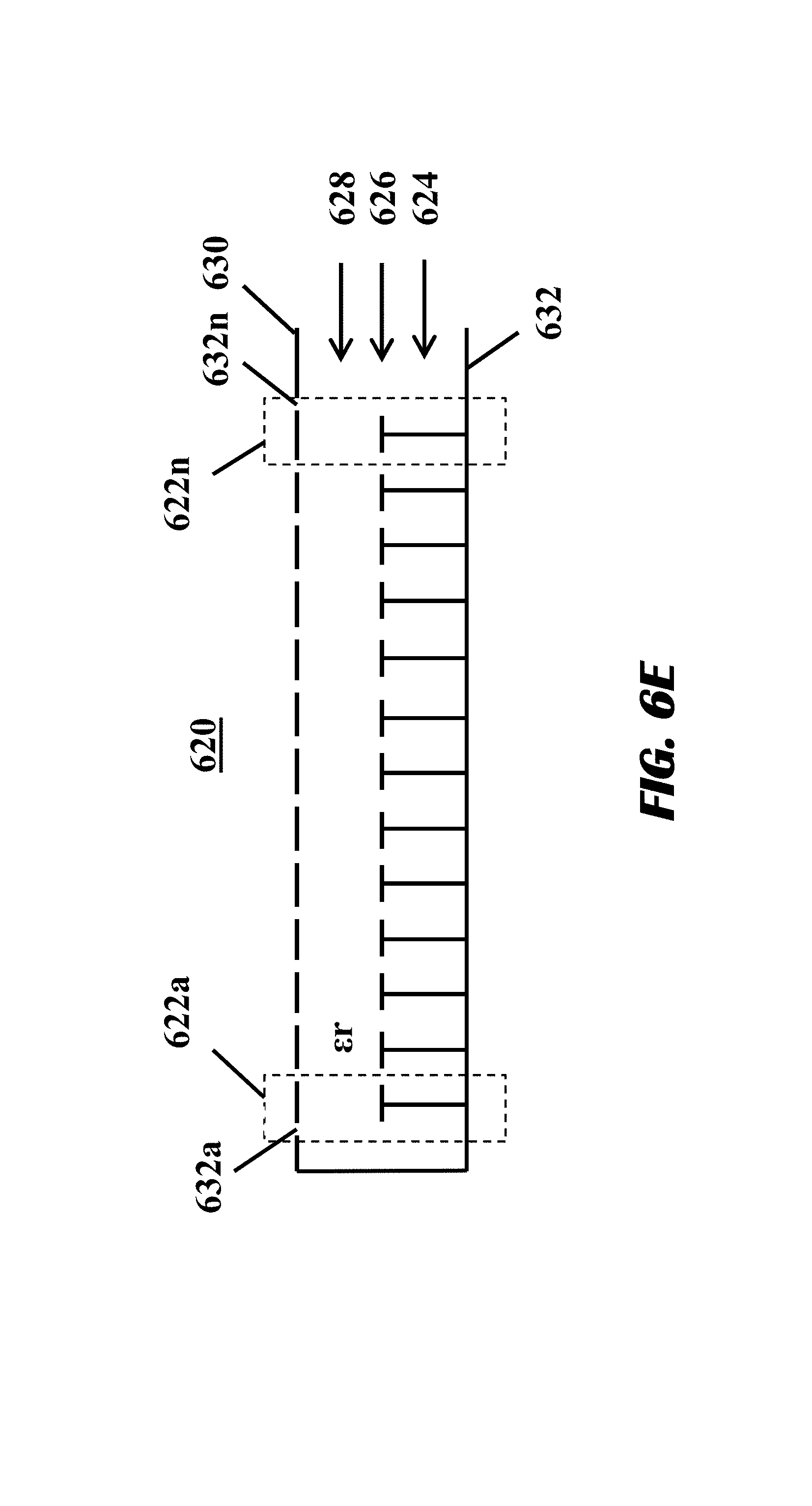
D00017

D00018
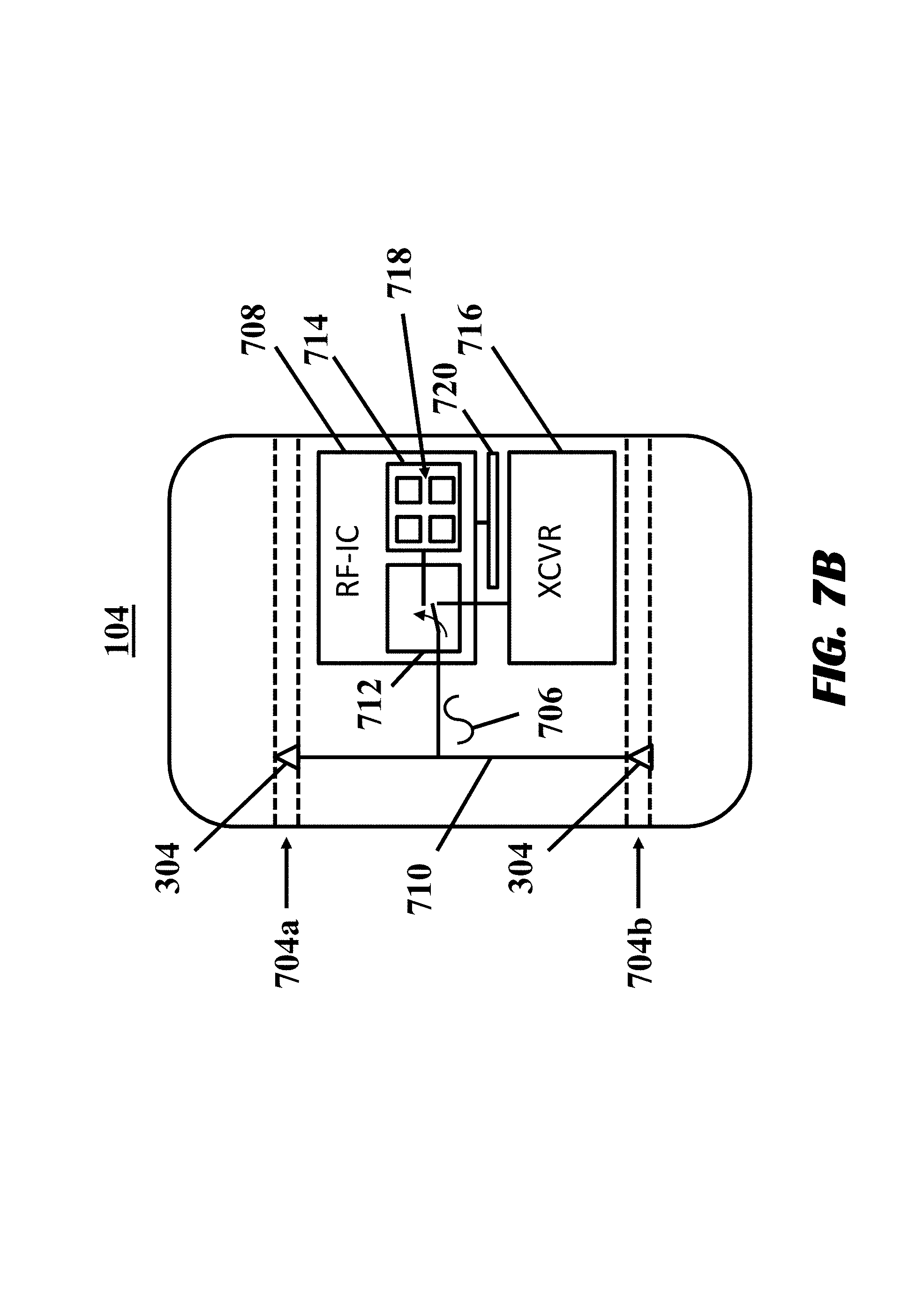
D00019
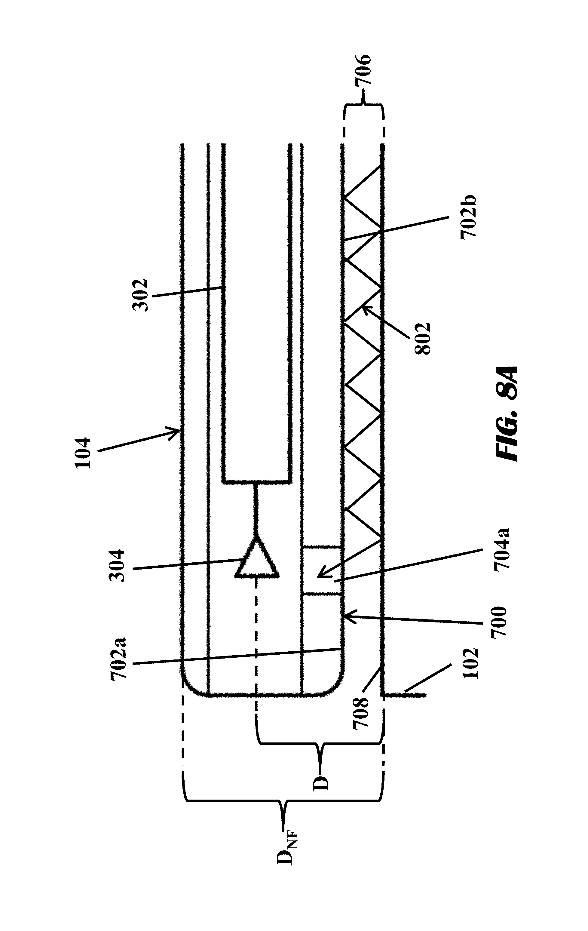
D00020
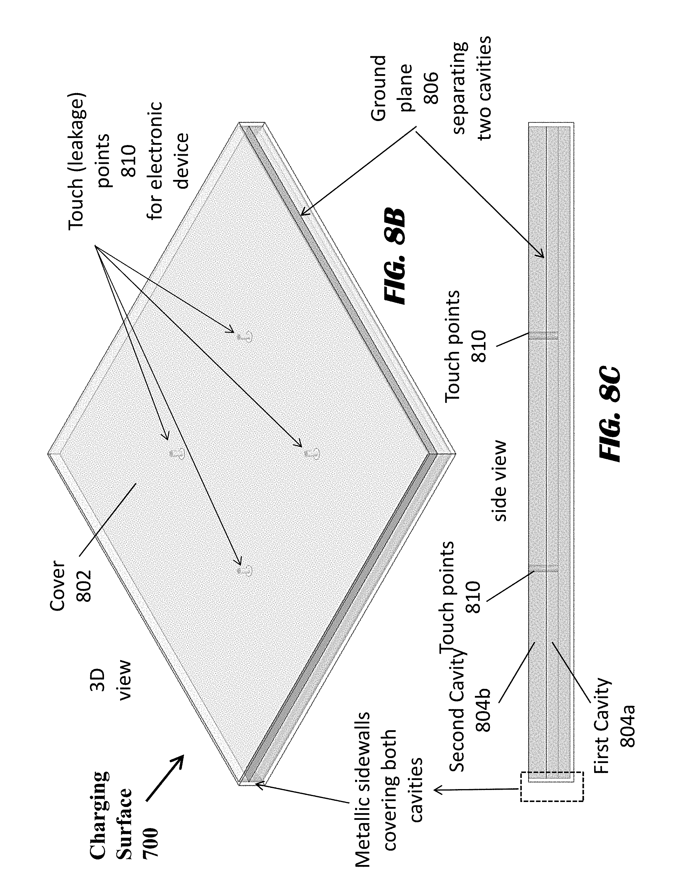
D00021
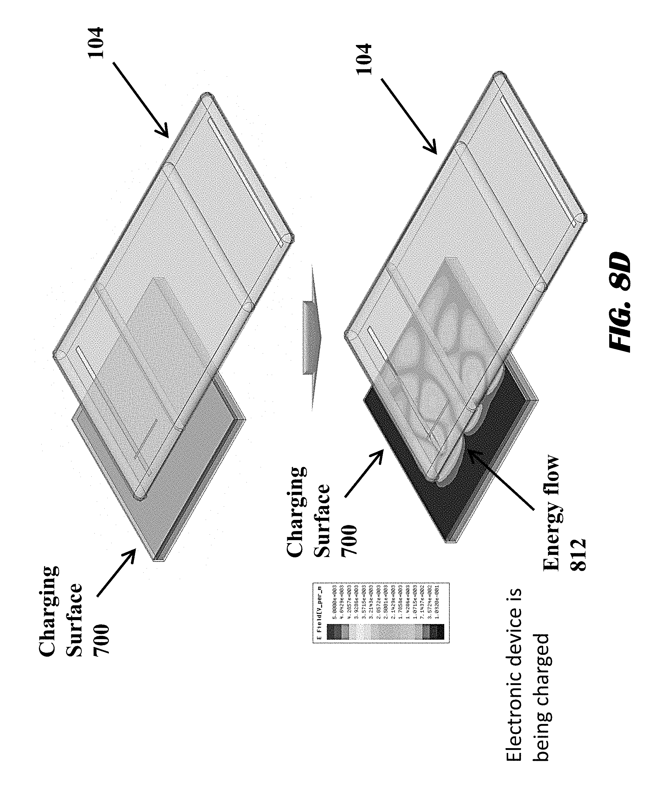
D00022
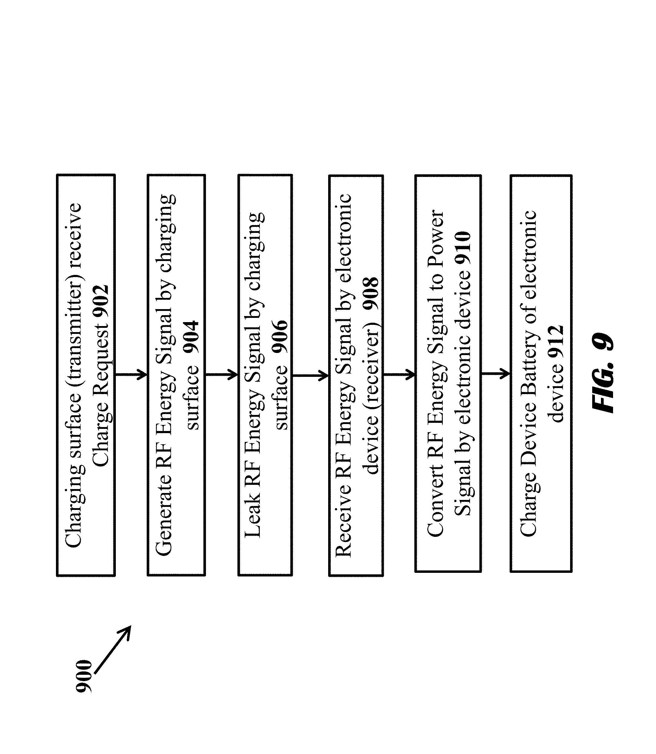
D00023
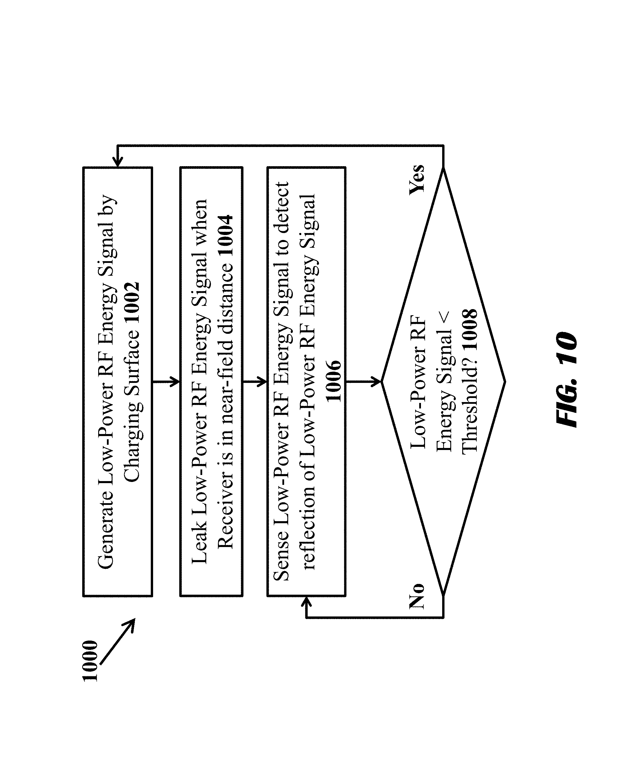
D00024

D00025

XML
uspto.report is an independent third-party trademark research tool that is not affiliated, endorsed, or sponsored by the United States Patent and Trademark Office (USPTO) or any other governmental organization. The information provided by uspto.report is based on publicly available data at the time of writing and is intended for informational purposes only.
While we strive to provide accurate and up-to-date information, we do not guarantee the accuracy, completeness, reliability, or suitability of the information displayed on this site. The use of this site is at your own risk. Any reliance you place on such information is therefore strictly at your own risk.
All official trademark data, including owner information, should be verified by visiting the official USPTO website at www.uspto.gov. This site is not intended to replace professional legal advice and should not be used as a substitute for consulting with a legal professional who is knowledgeable about trademark law.