Device having a single-sided printed circuit board
Teo Feb
U.S. patent number 10,206,282 [Application Number 15/328,322] was granted by the patent office on 2019-02-12 for device having a single-sided printed circuit board. This patent grant is currently assigned to Home Control Singapore PTE. LTD.. The grantee listed for this patent is Home Control Singapore PTE. LTD.. Invention is credited to Eng Kim Teo.


| United States Patent | 10,206,282 |
| Teo | February 12, 2019 |
Device having a single-sided printed circuit board
Abstract
A device comprising a single-sided printed circuit board (PCB) having a non-metallized hole, and a connection area (CA) close to the non-metallized hole on a metallized side of the single-sided printed circuit board. The present invention provides a conducting bridge (CP) from the connection area (CA) and at least partially covering the non-metallized hole, for allowing the connection area (CA) to be contacted, e.g. by a probe (P), from a non-metallized side of the single-sided printed circuit board (PCB) through the non-metallized hole.
| Inventors: | Teo; Eng Kim (Singapore, SG) | ||||||||||
|---|---|---|---|---|---|---|---|---|---|---|---|
| Applicant: |
|
||||||||||
| Assignee: | Home Control Singapore PTE.
LTD. (New Tech Park, SG) |
||||||||||
| Family ID: | 51390047 | ||||||||||
| Appl. No.: | 15/328,322 | ||||||||||
| Filed: | August 24, 2015 | ||||||||||
| PCT Filed: | August 24, 2015 | ||||||||||
| PCT No.: | PCT/SG2015/000137 | ||||||||||
| 371(c)(1),(2),(4) Date: | January 23, 2017 | ||||||||||
| PCT Pub. No.: | WO2016/032395 | ||||||||||
| PCT Pub. Date: | March 03, 2016 |
Prior Publication Data
| Document Identifier | Publication Date | |
|---|---|---|
| US 20170215283 A1 | Jul 27, 2017 | |
Foreign Application Priority Data
| Aug 25, 2014 [EP] | 14182073 | |||
| Current U.S. Class: | 1/1 |
| Current CPC Class: | H05K 1/0268 (20130101); H05K 1/116 (20130101); H05K 3/365 (20130101); H05K 2201/0394 (20130101); H05K 2201/09063 (20130101); G08C 17/02 (20130101) |
| Current International Class: | H05K 1/00 (20060101); H05K 1/18 (20060101); H05K 1/11 (20060101); H05K 1/02 (20060101); H05K 7/00 (20060101); G08C 17/02 (20060101); H05K 3/36 (20060101) |
References Cited [Referenced By]
U.S. Patent Documents
| 4701579 | October 1987 | Kurachi |
| 5514842 | May 1996 | Sugii |
| 5883335 | March 1999 | Mizumoto et al. |
| 6285081 | September 2001 | Jackson |
| 6911608 | June 2005 | Levy |
| 7391342 | June 2008 | Mui |
| 7618846 | November 2009 | Pagaila et al. |
| 8115108 | February 2012 | Sakai |
| 8404989 | March 2013 | Han |
| 8896743 | November 2014 | Du |
| 2001/0050566 | December 2001 | Hacke |
| 2008/0230362 | September 2008 | Hsu |
| 2827640 | Jan 1980 | DE | |||
| 0 852 397 | Jul 1998 | EP | |||
| 2 991 459 | Mar 2016 | EP | |||
| WO 2000/11920 | Mar 2000 | WO | |||
Other References
|
Extended European Search Report for European Application No. 14182073.8 "Device having a single-sided printed circuit board," dated Feb. 25, 2015. cited by applicant . International Search Report and Written Opinion of International Application No. PCT/SG2015/000137 "Device Having a Single-Sided Printed Circuit Board," dated Oct. 6, 2015. cited by applicant. |
Primary Examiner: Semenenko; Yuriy
Attorney, Agent or Firm: Hamilton, Brook, Smith & Reynolds, P.C.
Claims
The invention claimed is:
1. A remote control device comprising: a single-sided printed circuit board (PCB) having a non-metalized hole, and a connection area (CA) adjacent to the non-metalized hole on a metalized side of the single-sided printed circuit board; and a conducting bridge from the connection area (CA) and at least partially covering the non-metalized hole, for allowing the connection area (CA) to be contacted by a probe from a non-metalized side of the single-sided printed circuit board (PCB) through the non-metalized hole; wherein the PCB,CA and conducting bridge are maintained within a housing in operatively connectable contact without the requirement of an adhesive, wherein, upon insertion of the probe through the non-metalized hole, an electrical connection is formed between the probe and the CA through the conducting bridge.
2. The remote control device as claimed in claim 1, further comprising a key-mat (KM) having a carbon print area, and the conducting bridge is formed by said carbon print area.
Description
This application is the U.S. National Stage of International Application No. PCT/SG2015/000137, filed Aug. 24, 2015, now published, which designates the U.S., published in English, and claims priority under 35 U.S.C. .sctn..sctn. 119 or 365(c) to European Application No. 14182073.8, filed Aug. 25, 2014, issued on Feb. 2, 2018 as EP 2 991 459 B1. The entire teachings of the above applications are incorporated herein by reference.
FIELD OF THE INVENTION
The invention relates to a device having a single-sided printed circuit board.
BACKGROUND OF THE INVENTION
Single-sided printed circuit boards are known in the art, and have the advantage that they are cheaper than double-sided printed circuit boards. However, the obvious disadvantage of a single-sided printed circuit board is that connections are only possible at one side. While metallized vias or holes through the printed circuit board are known as well, such metallized holes also result in a price increase. For general background information on printed circuit boards (alternatively called printed wiring boards), reference is made to the Wikipedia article at http://en.wikipedia.org/wiki/Printed_wiring_board, incorporated herein by reference.
SUMMARY OF THE INVENTION
It is, inter alia, an object of the invention to provide a relatively low-cost device having a single-sided printed circuit board that can still be contacted from the other side without using a metallized via. The invention is defined by the independent claims. Advantageous embodiments are defined in the dependent claims.
One aspect of the invention provides a device comprising a single-sided printed circuit board having a non-metallized hole, and a connection area close to the non-metallized hole on a metallized side of the single-sided printed circuit board; and a conducting bridge from the connection area and at least partially covering the non-metallized hole, for allowing the connection area to be contacted (e.g. by a probe) from a non-metallized side of the single-sided printed circuit board through the non-metallized hole.
The invention is advantageously applied in a remote control device, in which case the connection bridge can be formed by part of a key-mat having a carbon print area that forms the connection bridge. The probe can be used for testing purposes, or for allowing the IC to be programmed. In a similar way, it is possible to make a reset button at the bottom side of a single-sided printed circuit board if that reset button bridges two connection areas on the wired top side of the printed circuit board via respective connection bridges.
These and other aspects of the invention will be apparent from and elucidated with reference to the embodiments described hereinafter.
BRIEF DESCRIPTION OF THE DRAWINGS
FIGS. 1A and 1B show exploded views of a remote control device in accordance with an embodiment of the invention; and
FIGS. 2 and 3 show other views of a remote control device in accordance with an embodiment of the invention.
DESCRIPTION OF EMBODIMENTS
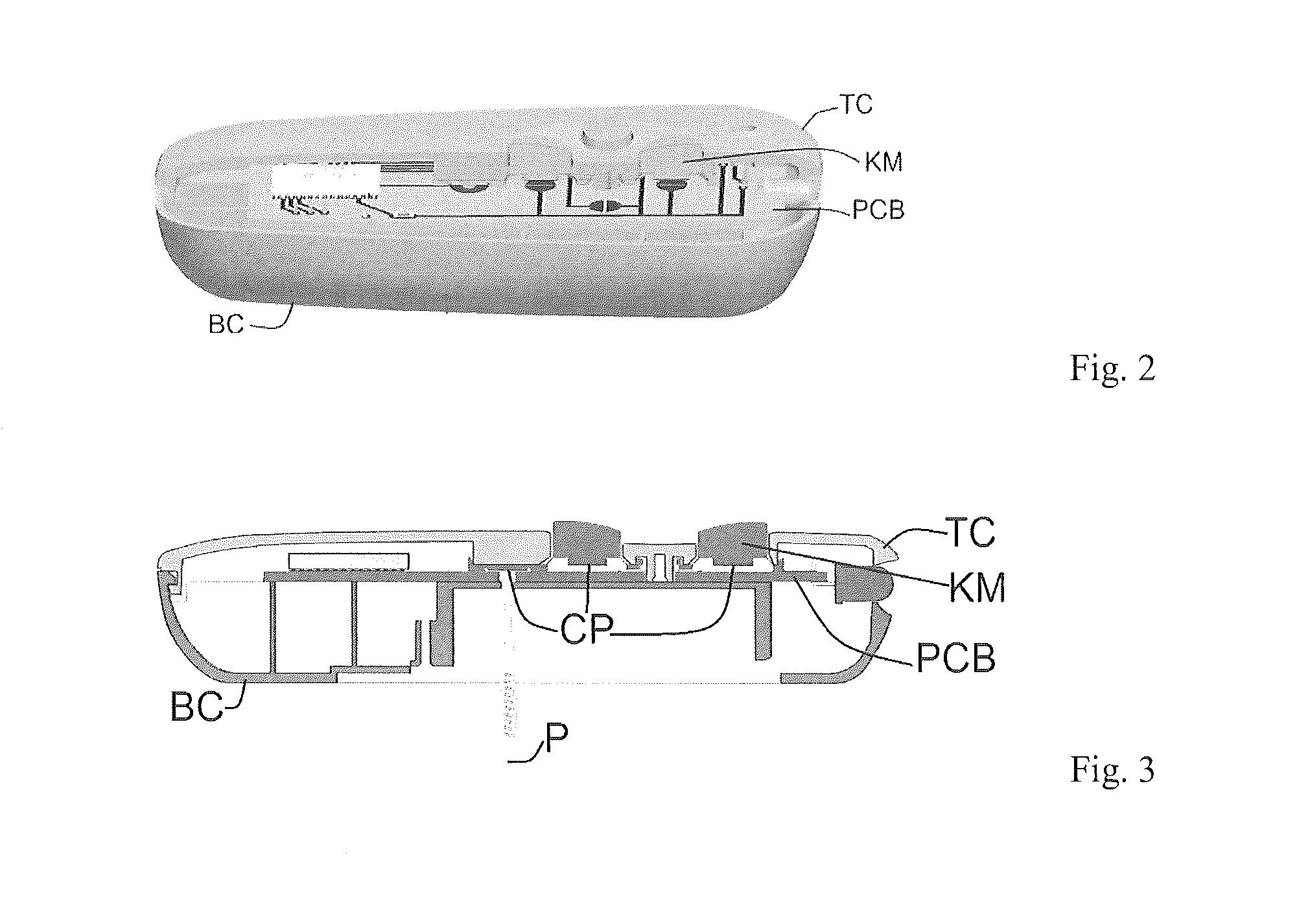
In the various figures, the reference signs have the following meanings:
TC top casing of the remote control device
KM key-mat
B button on the key-mat
CP carbon print area on the bottom of the key-mat
PCB printed circuit board
CA connection area on the printed circuit board
BC bottom casing of the remote control device
BL battery lid
P probe
The figures show various views of a remote control device in accordance with an embodiment of the invention. The embodiment is a rather simple remote control, with buttons B for channel up, channel down, volume up, volume down, and a standby button. Of course, the invention can alternatively be used with remote controls having more buttons. When a button is pressed down, a carbon print area CP on the lower side of the key-mat KM makes a connection on the printed circuit board PCB by bridging two contact areas (in this embodiment, these contact areas are represented by half circles; contact areas having other shapes are alternatively possible). The printed circuit board PCB has several other components customary for a remote control device, such as an integrated circuit and an infra-red light emitting diode.
In accordance with the present embodiment of the invention, there is also a carbon print area CP on the key-mat KM that is not below a button B, but that serves to make a connection between a probe P if and when inserted from the bottom side of the printed circuit board, through a hole in the bottom casing BC and a matching hole in the printed circuit board PCB, to a connection area CA on the top side of the single-sided printed circuit board PCB.
As shown in FIGS. 2 and 3, the top casing TC of the remote control device in accordance with the embodiment of the invention is preferably formed such that the carbon print area above the hole in the printed circuit board PCB is firmly pressed onto the connection area, so that if and when the probe P is inserted through the hole and touches the carbon print, it gets a good connection with the connection area.
It should be noted that the above-mentioned embodiments illustrate rather than limit the invention, and that those skilled in the art will be able to design many alternative embodiments without departing from the scope of the appended claims. In the shown embodiment, the connection area CA is a circle around the hole in the printed circuit board PCB. Alternatively, it may be a metalized area adjacent to just one side of the hole. The carbon print areas CP do not need to have a circle shape, and they do not need to cover the entire hole as long as they ensure that a connection is made between a probe P inserted through the hole and the connection area CA. The bottom side of the key-mat KM may alternatively have metallized contact areas instead of carbon print areas, as all what matters is that an electrical connection can be made so that a conducting bridge is formed. While the invention is illustrated by means of an embodiment formed by a remote control device, the invention can be used with any device having a single side printed circuit board that needs to be contacted from the other side. In the claims, any reference signs placed between parentheses shall not be construed as limiting the claim. The word "comprising" does not exclude the presence of elements or steps other than those listed in a claim. The word "a" or "an" preceding an element does not exclude the presence of a plurality of such elements.
* * * * *
References
D00000
D00001
D00002
XML
uspto.report is an independent third-party trademark research tool that is not affiliated, endorsed, or sponsored by the United States Patent and Trademark Office (USPTO) or any other governmental organization. The information provided by uspto.report is based on publicly available data at the time of writing and is intended for informational purposes only.
While we strive to provide accurate and up-to-date information, we do not guarantee the accuracy, completeness, reliability, or suitability of the information displayed on this site. The use of this site is at your own risk. Any reliance you place on such information is therefore strictly at your own risk.
All official trademark data, including owner information, should be verified by visiting the official USPTO website at www.uspto.gov. This site is not intended to replace professional legal advice and should not be used as a substitute for consulting with a legal professional who is knowledgeable about trademark law.