Re-interpolation with edge detection for extracting an aging pattern for AMOLED displays
Chaji , et al. Fe
U.S. patent number 10,198,979 [Application Number 15/783,852] was granted by the patent office on 2019-02-05 for re-interpolation with edge detection for extracting an aging pattern for amoled displays. This patent grant is currently assigned to Ignis Innovation Inc.. The grantee listed for this patent is Ignis Innovation Inc.. Invention is credited to Gholamreza Chaji, Mehdi Torbatian.


View All Diagrams
| United States Patent | 10,198,979 |
| Chaji , et al. | February 5, 2019 |
Re-interpolation with edge detection for extracting an aging pattern for AMOLED displays
Abstract
A method that includes an initial uniform pixel measurement and interpolation followed by an edge detection algorithm to recognize the areas that contribute mostly to the estimation error due to the interpolation. The pixels on the detected edges and around their vicinity are also measured, and an aging pattern of the entire display is obtained by re-interpolating the entire measured set of data for the initially measured pixels as well as the pixels around the detected edges. The estimation error is reduced particularly in the presence of aging patterns having highly spatially correlated areas with distinctive edges.
| Inventors: | Chaji; Gholamreza (Waterloo, CA), Torbatian; Mehdi (Waterloo, CA) | ||||||||||
|---|---|---|---|---|---|---|---|---|---|---|---|
| Applicant: |
|
||||||||||
| Assignee: | Ignis Innovation Inc.
(Waterloo, Ontario, unknown) |
||||||||||
| Family ID: | 50241141 | ||||||||||
| Appl. No.: | 15/783,852 | ||||||||||
| Filed: | October 13, 2017 |
Prior Publication Data
| Document Identifier | Publication Date | |
|---|---|---|
| US 20180040269 A1 | Feb 8, 2018 | |
Related U.S. Patent Documents
| Application Number | Filing Date | Patent Number | Issue Date | ||
|---|---|---|---|---|---|
| 15363290 | Nov 29, 2016 | 9818323 | |||
| 15050700 | Jan 3, 2017 | 9536465 | |||
| 14209392 | Apr 5, 2016 | 9305488 | |||
| 61783537 | Mar 14, 2013 | ||||
| Current U.S. Class: | 1/1 |
| Current CPC Class: | G09G 3/2003 (20130101); G09G 3/3208 (20130101); G09G 3/3225 (20130101); G09G 3/3233 (20130101); G09G 5/026 (20130101); G09G 3/2085 (20130101); G09G 3/006 (20130101); G09G 3/2007 (20130101); G06T 3/403 (20130101); G09G 2340/10 (20130101); G09G 2320/0693 (20130101); G09G 2320/0242 (20130101); G09G 2320/045 (20130101); G09G 2320/043 (20130101); G09G 2320/0233 (20130101) |
| Current International Class: | G06T 3/40 (20060101); G09G 3/3208 (20160101); G09G 5/02 (20060101); G09G 3/20 (20060101); G09G 3/3225 (20160101); G09G 3/00 (20060101); G09G 3/3233 (20160101) |
References Cited [Referenced By]
U.S. Patent Documents
| 3506851 | April 1970 | Polkinghorn |
| 3774055 | November 1973 | Bapat |
| 4090096 | May 1978 | Nagami |
| 4160934 | July 1979 | Kirsch |
| 4295091 | October 1981 | Ponkala |
| 4354162 | October 1982 | Wright |
| 4943956 | July 1990 | Noro |
| 4996523 | February 1991 | Bell |
| 5153420 | October 1992 | Hack |
| 5198803 | March 1993 | Shie |
| 5204661 | April 1993 | Hack |
| 5266515 | November 1993 | Robb |
| 5489918 | February 1996 | Mosier |
| 5498880 | March 1996 | Lee |
| 5557342 | September 1996 | Eto |
| 5561381 | October 1996 | Jenkins et al. |
| 5572444 | November 1996 | Lentz |
| 5589847 | December 1996 | Lewis |
| 5619033 | April 1997 | Weisfield |
| 5648276 | July 1997 | Hara |
| 5670973 | September 1997 | Bassetti |
| 5684365 | November 1997 | Tang |
| 5691783 | November 1997 | Numao |
| 5714968 | February 1998 | Ikeda |
| 5723950 | March 1998 | Wei |
| 5744824 | April 1998 | Kousai |
| 5745660 | April 1998 | Kolpatzik |
| 5748160 | May 1998 | Shieh |
| 5815303 | September 1998 | Berlin |
| 5870071 | February 1999 | Kawahata |
| 5874803 | February 1999 | Garbuzov |
| 5880582 | March 1999 | Sawada |
| 5903248 | May 1999 | Irwin |
| 5917280 | June 1999 | Burrows |
| 5923794 | July 1999 | McGrath |
| 5945972 | August 1999 | Okumura |
| 5949398 | September 1999 | Kim |
| 5952789 | September 1999 | Stewart |
| 5952991 | September 1999 | Akiyama |
| 5982104 | November 1999 | Sasaki |
| 5990629 | November 1999 | Yamada |
| 6023259 | February 2000 | Howard |
| 6069365 | May 2000 | Chow |
| 6091203 | July 2000 | Kawashima |
| 6097360 | August 2000 | Holloman |
| 6144222 | November 2000 | Ho |
| 6177915 | January 2001 | Beeteson |
| 6229506 | May 2001 | Dawson |
| 6229508 | May 2001 | Kane |
| 6246180 | June 2001 | Nishigaki |
| 6252248 | June 2001 | Sano |
| 6259424 | July 2001 | Kurogane |
| 6262589 | July 2001 | Tamukai |
| 6271825 | August 2001 | Greene |
| 6288696 | September 2001 | Holloman |
| 6304039 | October 2001 | Appelberg |
| 6307322 | October 2001 | Dawson |
| 6310962 | October 2001 | Chung |
| 6320325 | November 2001 | Cok |
| 6323631 | November 2001 | Juang |
| 6329971 | December 2001 | McKnight |
| 6356029 | March 2002 | Hunter |
| 6373454 | April 2002 | Knapp |
| 6377237 | April 2002 | Sojourner |
| 6392617 | May 2002 | Gleason |
| 6404139 | June 2002 | Sasaki et al. |
| 6414661 | July 2002 | Shen |
| 6417825 | July 2002 | Stewart |
| 6433488 | August 2002 | Bu |
| 6437106 | August 2002 | Stoner |
| 6445369 | September 2002 | Yang |
| 6475845 | November 2002 | Kimura |
| 6501098 | December 2002 | Yamazaki |
| 6501466 | December 2002 | Yamagishi |
| 6518962 | February 2003 | Kimura |
| 6522315 | February 2003 | Ozawa |
| 6525683 | February 2003 | Gu |
| 6531827 | March 2003 | Kawashima |
| 6541921 | April 2003 | Luciano, Jr. et al. |
| 6542138 | April 2003 | Shannon |
| 6555420 | April 2003 | Yamazaki |
| 6577302 | June 2003 | Hunter |
| 6580408 | June 2003 | Bae |
| 6580657 | June 2003 | Sanford |
| 6583398 | June 2003 | Harkin |
| 6583775 | June 2003 | Sekiya |
| 6594606 | July 2003 | Everitt |
| 6618030 | September 2003 | Kane |
| 6639244 | October 2003 | Yamazaki |
| 6668645 | December 2003 | Gilmour |
| 6677713 | January 2004 | Sung |
| 6680580 | January 2004 | Sung |
| 6687266 | February 2004 | Ma |
| 6690000 | February 2004 | Muramatsu |
| 6690344 | February 2004 | Takeuchi |
| 6693388 | February 2004 | Oomura |
| 6693610 | February 2004 | Shannon |
| 6697057 | February 2004 | Koyama |
| 6720942 | April 2004 | Lee |
| 6724151 | April 2004 | Yoo |
| 6734636 | May 2004 | Sanford |
| 6738034 | May 2004 | Kaneko |
| 6738035 | May 2004 | Fan |
| 6753655 | June 2004 | Shih |
| 6753834 | June 2004 | Mikami |
| 6756741 | June 2004 | Li |
| 6756952 | June 2004 | Decaux |
| 6756958 | June 2004 | Furuhashi |
| 6765549 | July 2004 | Yamazaki et al. |
| 6771028 | August 2004 | Winters |
| 6777712 | August 2004 | Sanford |
| 6777888 | August 2004 | Kondo |
| 6781306 | August 2004 | Park |
| 6781567 | August 2004 | Kimura |
| 6806497 | October 2004 | Jo |
| 6806638 | October 2004 | Lih et al. |
| 6806857 | October 2004 | Sempel |
| 6809706 | October 2004 | Shimoda |
| 6815975 | November 2004 | Nara |
| 6828950 | December 2004 | Koyama |
| 6853371 | February 2005 | Miyajima |
| 6859193 | February 2005 | Yumoto |
| 6873117 | March 2005 | Ishizuka |
| 6876346 | April 2005 | Anzai |
| 6885356 | April 2005 | Hashimoto |
| 6900485 | May 2005 | Lee |
| 6903734 | June 2005 | Eu |
| 6909243 | June 2005 | Inukai |
| 6909419 | June 2005 | Zavracky |
| 6911960 | June 2005 | Yokoyama |
| 6911964 | June 2005 | Lee |
| 6914448 | July 2005 | Jinno |
| 6919871 | July 2005 | Kwon |
| 6924602 | August 2005 | Komiya |
| 6937215 | August 2005 | Lo |
| 6937220 | August 2005 | Kitaura |
| 6940214 | September 2005 | Komiya |
| 6943500 | September 2005 | LeChevalier |
| 6947022 | September 2005 | McCartney |
| 6954194 | October 2005 | Matsumoto |
| 6956547 | October 2005 | Bae |
| 6975142 | December 2005 | Azami |
| 6975332 | December 2005 | Arnold |
| 6995510 | February 2006 | Murakami |
| 6995519 | February 2006 | Arnold |
| 7023408 | April 2006 | Chen |
| 7027015 | April 2006 | Booth, Jr. |
| 7027078 | April 2006 | Reihl |
| 7034793 | April 2006 | Sekiya |
| 7038392 | May 2006 | Libsch |
| 7053875 | May 2006 | Chou |
| 7057359 | June 2006 | Hung |
| 7061451 | June 2006 | Kimura |
| 7064733 | June 2006 | Cok |
| 7071932 | July 2006 | Libsch |
| 7088051 | August 2006 | Cok |
| 7088052 | August 2006 | Kimura |
| 7102378 | September 2006 | Kuo |
| 7106285 | September 2006 | Naugler |
| 7112820 | September 2006 | Chang |
| 7116058 | October 2006 | Lo |
| 7119493 | October 2006 | Fryer |
| 7122835 | October 2006 | Ikeda |
| 7127380 | October 2006 | Iverson |
| 7129914 | October 2006 | Knapp |
| 7161566 | January 2007 | Cok |
| 7164417 | January 2007 | Cok |
| 7193589 | March 2007 | Yoshida |
| 7224332 | May 2007 | Cok |
| 7227519 | June 2007 | Kawase |
| 7245277 | July 2007 | Ishizuka |
| 7246912 | July 2007 | Burger et al. |
| 7248236 | July 2007 | Nathan |
| 7262753 | August 2007 | Tanghe |
| 7274363 | September 2007 | Ishizuka |
| 7310092 | December 2007 | Imamura |
| 7315295 | January 2008 | Kimura |
| 7321348 | January 2008 | Cok |
| 7339560 | March 2008 | Sun |
| 7355574 | April 2008 | Leon |
| 7358941 | April 2008 | Ono |
| 7368868 | May 2008 | Sakamoto |
| 7397485 | July 2008 | Miller |
| 7411571 | August 2008 | Huh |
| 7414600 | August 2008 | Nathan |
| 7423617 | September 2008 | Giraldo |
| 7453054 | November 2008 | Lee |
| 7474285 | January 2009 | Kimura |
| 7502000 | March 2009 | Yuki |
| 7528812 | May 2009 | Tsuge |
| 7535449 | May 2009 | Miyazawa |
| 7554512 | June 2009 | Steer |
| 7569849 | August 2009 | Nathan |
| 7576718 | August 2009 | Miyazawa |
| 7580012 | August 2009 | Kim |
| 7589707 | September 2009 | Chou |
| 7605792 | October 2009 | Son |
| 7609239 | October 2009 | Chang |
| 7619594 | November 2009 | Hu |
| 7619597 | November 2009 | Nathan |
| 7633470 | December 2009 | Kane |
| 7656370 | February 2010 | Schneider |
| 7675485 | March 2010 | Steer |
| 7800558 | September 2010 | Routley |
| 7847764 | December 2010 | Cok |
| 7859492 | December 2010 | Kohno |
| 7868859 | January 2011 | Tomida |
| 7876294 | January 2011 | Sasaki |
| 7924249 | April 2011 | Nathan |
| 7932883 | April 2011 | Klompenhouwer |
| 7969390 | June 2011 | Yoshida |
| 7978187 | July 2011 | Nathan |
| 7994712 | August 2011 | Sung |
| 8026876 | September 2011 | Nathan |
| 8031180 | October 2011 | Miyamoto et al. |
| 8049420 | November 2011 | Tamura |
| 8077123 | December 2011 | Naugler, Jr. |
| 8115707 | February 2012 | Nathan |
| 8208084 | June 2012 | Lin |
| 8223177 | July 2012 | Nathan |
| 8232939 | July 2012 | Nathan |
| 8259044 | September 2012 | Nathan |
| 8264431 | September 2012 | Bulovic |
| 8279143 | October 2012 | Nathan |
| 8294696 | October 2012 | Min et al. |
| 8314783 | November 2012 | Sambandan et al. |
| 8339386 | December 2012 | Leon |
| 8441206 | May 2013 | Myers |
| 8493296 | July 2013 | Ogawa |
| 8581809 | November 2013 | Nathan et al. |
| 8654114 | February 2014 | Shimizu |
| 9125278 | September 2015 | Nathan et al. |
| 9368063 | June 2016 | Chaji |
| 9418587 | August 2016 | Chaji |
| 9430958 | August 2016 | Chaji |
| 9472139 | October 2016 | Nathan |
| 9489891 | November 2016 | Nathan |
| 9489897 | November 2016 | Jaffari |
| 9502653 | November 2016 | Chaji |
| 9530349 | December 2016 | Chaji |
| 9530352 | December 2016 | Nathan |
| 9536460 | January 2017 | Chaji |
| 9536465 | January 2017 | Chaji |
| 9589490 | March 2017 | Chaji |
| 9633597 | April 2017 | Nathan |
| 9640112 | May 2017 | Jaffari |
| 9721512 | August 2017 | Soni |
| 9741279 | August 2017 | Chaji |
| 9741282 | August 2017 | Giannikouris |
| 9761170 | September 2017 | Chaji |
| 9773439 | September 2017 | Chaji |
| 9773441 | September 2017 | Chaji |
| 9786209 | October 2017 | Chaji |
| 2001/0002703 | June 2001 | Koyama |
| 2001/0009283 | July 2001 | Arao |
| 2001/0024181 | September 2001 | Kubota |
| 2001/0024186 | September 2001 | Kane |
| 2001/0026257 | October 2001 | Kimura |
| 2001/0030323 | October 2001 | Ikeda |
| 2001/0035863 | November 2001 | Kimura |
| 2001/0038367 | November 2001 | Inukai |
| 2001/0040541 | November 2001 | Yoneda |
| 2001/0043173 | November 2001 | Troutman |
| 2001/0045929 | November 2001 | Prache |
| 2001/0052606 | December 2001 | Sempel |
| 2001/0052940 | December 2001 | Hagihara |
| 2002/0000576 | January 2002 | Inukai |
| 2002/0011796 | January 2002 | Koyama |
| 2002/0011799 | January 2002 | Kimura |
| 2002/0012057 | January 2002 | Kimura |
| 2002/0014851 | February 2002 | Tai |
| 2002/0018034 | February 2002 | Ohki |
| 2002/0030190 | March 2002 | Ohtani |
| 2002/0047565 | April 2002 | Nara |
| 2002/0052086 | May 2002 | Maeda |
| 2002/0067134 | June 2002 | Kawashima |
| 2002/0084463 | July 2002 | Sanford |
| 2002/0101152 | August 2002 | Kimura |
| 2002/0101172 | August 2002 | Bu |
| 2002/0105279 | August 2002 | Kimura |
| 2002/0117722 | August 2002 | Osada |
| 2002/0122308 | September 2002 | Ikeda |
| 2002/0158587 | October 2002 | Komiya |
| 2002/0158666 | October 2002 | Azami |
| 2002/0158823 | October 2002 | Zavracky |
| 2002/0167471 | November 2002 | Everitt |
| 2002/0167474 | November 2002 | Everitt |
| 2002/0169575 | November 2002 | Everitt |
| 2002/0180369 | December 2002 | Koyama |
| 2002/0180721 | December 2002 | Kimura |
| 2002/0181276 | December 2002 | Yamazaki |
| 2002/0183945 | December 2002 | Everitt |
| 2002/0186214 | December 2002 | Siwinski |
| 2002/0190924 | December 2002 | Asano |
| 2002/0190971 | December 2002 | Nakamura |
| 2002/0195967 | December 2002 | Kim |
| 2002/0195968 | December 2002 | Sanford |
| 2003/0020413 | January 2003 | Oomura |
| 2003/0030603 | February 2003 | Shimoda |
| 2003/0043088 | March 2003 | Booth |
| 2003/0057895 | March 2003 | Kimura |
| 2003/0058226 | March 2003 | Bertram |
| 2003/0062524 | April 2003 | Kimura |
| 2003/0063081 | April 2003 | Kimura |
| 2003/0071821 | April 2003 | Sundahl |
| 2003/0076048 | April 2003 | Rutherford |
| 2003/0090447 | May 2003 | Kimura |
| 2003/0090481 | May 2003 | Kimura |
| 2003/0107560 | June 2003 | Yumoto |
| 2003/0111966 | June 2003 | Mikami |
| 2003/0122745 | July 2003 | Miyazawa |
| 2003/0122749 | July 2003 | Booth, Jr. et al. |
| 2003/0122813 | July 2003 | Ishizuki |
| 2003/0142088 | July 2003 | LeChevalier |
| 2003/0146897 | August 2003 | Hunter |
| 2003/0151569 | August 2003 | Lee |
| 2003/0156101 | August 2003 | Le Chevalier |
| 2003/0169241 | September 2003 | LeChevalier |
| 2003/0174152 | September 2003 | Noguchi |
| 2003/0179626 | September 2003 | Sanford |
| 2003/0185438 | October 2003 | Osawa |
| 2003/0197663 | October 2003 | Lee |
| 2003/0210256 | November 2003 | Mori |
| 2003/0230141 | December 2003 | Gilmour |
| 2003/0230980 | December 2003 | Forrest |
| 2003/0231148 | December 2003 | Lin |
| 2004/0032382 | February 2004 | Cok |
| 2004/0041750 | March 2004 | Abe |
| 2004/0066357 | April 2004 | Kawasaki |
| 2004/0070557 | April 2004 | Asano |
| 2004/0070565 | April 2004 | Nayar |
| 2004/0090186 | May 2004 | Kanauchi |
| 2004/0090400 | May 2004 | Yoo |
| 2004/0095297 | May 2004 | Libsch |
| 2004/0100427 | May 2004 | Miyazawa |
| 2004/0108518 | June 2004 | Jo |
| 2004/0135749 | July 2004 | Kondakov |
| 2004/0140982 | July 2004 | Pate |
| 2004/0145547 | July 2004 | Oh |
| 2004/0150592 | August 2004 | Mizukoshi |
| 2004/0150594 | August 2004 | Koyama |
| 2004/0150595 | August 2004 | Kasai |
| 2004/0155841 | August 2004 | Kasai |
| 2004/0174347 | September 2004 | Sun |
| 2004/0174349 | September 2004 | Libsch |
| 2004/0174354 | September 2004 | Ono |
| 2004/0178743 | September 2004 | Miller |
| 2004/0183759 | September 2004 | Stevenson |
| 2004/0196275 | October 2004 | Hattori |
| 2004/0207615 | October 2004 | Yumoto |
| 2004/0227697 | November 2004 | Mori |
| 2004/0233125 | November 2004 | Tanghe |
| 2004/0239596 | December 2004 | Ono |
| 2004/0246246 | December 2004 | Tobita |
| 2004/0252089 | December 2004 | Ono |
| 2004/0257313 | December 2004 | Kawashima |
| 2004/0257353 | December 2004 | Imamura |
| 2004/0257355 | December 2004 | Naugler |
| 2004/0263437 | December 2004 | Hattori |
| 2004/0263444 | December 2004 | Kimura |
| 2004/0263445 | December 2004 | Inukai |
| 2004/0263541 | December 2004 | Takeuchi |
| 2005/0007355 | January 2005 | Miura |
| 2005/0007357 | January 2005 | Yamashita |
| 2005/0007392 | January 2005 | Kasai |
| 2005/0017650 | January 2005 | Fryer |
| 2005/0024081 | February 2005 | Kuo |
| 2005/0024393 | February 2005 | Kondo |
| 2005/0030267 | February 2005 | Tanghe |
| 2005/0057484 | March 2005 | Diefenbaugh |
| 2005/0057580 | March 2005 | Yamano |
| 2005/0067970 | March 2005 | Libsch |
| 2005/0067971 | March 2005 | Kane |
| 2005/0068270 | March 2005 | Awakura |
| 2005/0068275 | March 2005 | Kane |
| 2005/0073264 | April 2005 | Matsumoto |
| 2005/0083323 | April 2005 | Suzuki |
| 2005/0088103 | April 2005 | Kageyama |
| 2005/0105031 | May 2005 | Shih |
| 2005/0110420 | May 2005 | Arnold |
| 2005/0110807 | May 2005 | Chang |
| 2005/0122294 | June 2005 | Ben-David |
| 2005/0140598 | June 2005 | Kim |
| 2005/0140610 | June 2005 | Smith |
| 2005/0145891 | July 2005 | Abe |
| 2005/0156831 | July 2005 | Yamazaki |
| 2005/0162079 | July 2005 | Sakamoto |
| 2005/0168416 | August 2005 | Hashimoto |
| 2005/0179626 | August 2005 | Yuki |
| 2005/0179628 | August 2005 | Kimura |
| 2005/0185200 | August 2005 | Tobol |
| 2005/0200575 | September 2005 | Kim |
| 2005/0206590 | September 2005 | Sasaki |
| 2005/0212787 | September 2005 | Noguchi |
| 2005/0219184 | October 2005 | Zehner |
| 2005/0225683 | October 2005 | Nozawa |
| 2005/0248515 | November 2005 | Naugler |
| 2005/0269959 | December 2005 | Uchino |
| 2005/0269960 | December 2005 | Ono |
| 2005/0280615 | December 2005 | Cok |
| 2005/0280766 | December 2005 | Johnson |
| 2005/0285822 | December 2005 | Reddy |
| 2005/0285825 | December 2005 | Eom |
| 2006/0001613 | January 2006 | Routley |
| 2006/0007072 | January 2006 | Choi |
| 2006/0007206 | January 2006 | Reddy et al. |
| 2006/0007249 | January 2006 | Reddy |
| 2006/0012310 | January 2006 | Chen |
| 2006/0012311 | January 2006 | Ogawa |
| 2006/0015272 | January 2006 | Giraldo et al. |
| 2006/0022305 | February 2006 | Yamashita |
| 2006/0022907 | February 2006 | Uchino et al. |
| 2006/0027807 | February 2006 | Nathan |
| 2006/0030084 | February 2006 | Young |
| 2006/0038501 | February 2006 | Koyama et al. |
| 2006/0038758 | February 2006 | Routley |
| 2006/0038762 | February 2006 | Chou |
| 2006/0044227 | March 2006 | Hadcock |
| 2006/0061248 | March 2006 | Cok |
| 2006/0066533 | March 2006 | Sato |
| 2006/0077134 | April 2006 | Hector et al. |
| 2006/0077135 | April 2006 | Cok |
| 2006/0077142 | April 2006 | Kwon |
| 2006/0082523 | April 2006 | Guo |
| 2006/0092185 | May 2006 | Jo |
| 2006/0097628 | May 2006 | Suh |
| 2006/0097631 | May 2006 | Lee |
| 2006/0103324 | May 2006 | Kim et al. |
| 2006/0103611 | May 2006 | Choi |
| 2006/0125740 | June 2006 | Shirasaki et al. |
| 2006/0149493 | July 2006 | Sambandan |
| 2006/0170623 | August 2006 | Naugler, Jr. |
| 2006/0176250 | August 2006 | Nathan |
| 2006/0208961 | September 2006 | Nathan |
| 2006/0208971 | September 2006 | Deane |
| 2006/0214888 | September 2006 | Schneider |
| 2006/0231740 | October 2006 | Kasai |
| 2006/0232522 | October 2006 | Roy |
| 2006/0244697 | November 2006 | Lee |
| 2006/0256048 | November 2006 | Fish et al. |
| 2006/0261841 | November 2006 | Fish |
| 2006/0273997 | December 2006 | Nathan |
| 2006/0279481 | December 2006 | Haruna |
| 2006/0284801 | December 2006 | Yoon |
| 2006/0284802 | December 2006 | Kohno |
| 2006/0284895 | December 2006 | Marcu |
| 2006/0290614 | December 2006 | Nathan |
| 2006/0290618 | December 2006 | Goto |
| 2007/0001937 | January 2007 | Park |
| 2007/0001939 | January 2007 | Hashimoto |
| 2007/0008251 | January 2007 | Kohno |
| 2007/0008268 | January 2007 | Park |
| 2007/0008297 | January 2007 | Bassetti |
| 2007/0057873 | March 2007 | Uchino |
| 2007/0057874 | March 2007 | Le Roy |
| 2007/0069998 | March 2007 | Naugler |
| 2007/0075727 | April 2007 | Nakano |
| 2007/0076226 | April 2007 | Klompenhouwer |
| 2007/0080905 | April 2007 | Takahara |
| 2007/0080906 | April 2007 | Tanabe |
| 2007/0080908 | April 2007 | Nathan |
| 2007/0097038 | May 2007 | Yamazaki |
| 2007/0097041 | May 2007 | Park |
| 2007/0103411 | May 2007 | Cok et al. |
| 2007/0103419 | May 2007 | Uchino |
| 2007/0115221 | May 2007 | Buchhauser |
| 2007/0126672 | June 2007 | Tada et al. |
| 2007/0164664 | July 2007 | Ludwicki |
| 2007/0164937 | July 2007 | Jung et al. |
| 2007/0164938 | July 2007 | Shin |
| 2007/0182671 | August 2007 | Nathan |
| 2007/0236134 | October 2007 | Ho |
| 2007/0236440 | October 2007 | Wacyk |
| 2007/0236517 | October 2007 | Kimpe |
| 2007/0241999 | October 2007 | Lin |
| 2007/0273294 | November 2007 | Nagayama |
| 2007/0285359 | December 2007 | Ono |
| 2007/0290957 | December 2007 | Cok |
| 2007/0290958 | December 2007 | Cok |
| 2007/0296672 | December 2007 | Kim |
| 2008/0001525 | January 2008 | Chao |
| 2008/0001544 | January 2008 | Murakami |
| 2008/0030518 | February 2008 | Higgins |
| 2008/0036706 | February 2008 | Kitazawa |
| 2008/0036708 | February 2008 | Shirasaki |
| 2008/0042942 | February 2008 | Takahashi |
| 2008/0042948 | February 2008 | Yamashita |
| 2008/0048951 | February 2008 | Naugler, Jr. |
| 2008/0055209 | March 2008 | Cok |
| 2008/0055211 | March 2008 | Ogawa |
| 2008/0074413 | March 2008 | Ogura |
| 2008/0088549 | April 2008 | Nathan |
| 2008/0088648 | April 2008 | Nathan |
| 2008/0111766 | May 2008 | Uchino |
| 2008/0116787 | May 2008 | Hsu |
| 2008/0117144 | May 2008 | Nakano et al. |
| 2008/0136770 | June 2008 | Peker et al. |
| 2008/0150845 | June 2008 | Ishii |
| 2008/0150847 | June 2008 | Kim |
| 2008/0158115 | July 2008 | Cordes |
| 2008/0158648 | July 2008 | Cummings |
| 2008/0191976 | August 2008 | Nathan |
| 2008/0198103 | August 2008 | Toyomura |
| 2008/0211749 | September 2008 | Weitbruch |
| 2008/0218451 | September 2008 | Miyamoto |
| 2008/0231558 | September 2008 | Naugler |
| 2008/0231562 | September 2008 | Kwon |
| 2008/0231625 | September 2008 | Minami |
| 2008/0246713 | October 2008 | Lee |
| 2008/0252223 | October 2008 | Toyoda |
| 2008/0252571 | October 2008 | Hente |
| 2008/0259020 | October 2008 | Fisekovic |
| 2008/0290805 | November 2008 | Yamada |
| 2008/0297055 | December 2008 | Miyake |
| 2009/0033598 | February 2009 | Suh |
| 2009/0058772 | March 2009 | Lee |
| 2009/0109142 | April 2009 | Takahara |
| 2009/0121994 | May 2009 | Miyata |
| 2009/0146926 | June 2009 | Sung |
| 2009/0160743 | June 2009 | Tomida |
| 2009/0174628 | July 2009 | Wang |
| 2009/0184901 | July 2009 | Kwon |
| 2009/0195483 | August 2009 | Naugler, Jr. |
| 2009/0201281 | August 2009 | Routley |
| 2009/0206764 | August 2009 | Schemmann |
| 2009/0207160 | August 2009 | Shirasaki et al. |
| 2009/0213046 | August 2009 | Nam |
| 2009/0244046 | October 2009 | Seto |
| 2009/0262047 | October 2009 | Yamashita |
| 2010/0004891 | January 2010 | Ahlers |
| 2010/0026725 | February 2010 | Smith |
| 2010/0039422 | February 2010 | Seto |
| 2010/0039458 | February 2010 | Nathan |
| 2010/0045646 | February 2010 | Kishi |
| 2010/0045650 | February 2010 | Fish et al. |
| 2010/0060911 | March 2010 | Marcu |
| 2010/0073335 | March 2010 | Min et al. |
| 2010/0073357 | March 2010 | Min et al. |
| 2010/0079419 | April 2010 | Shibusawa |
| 2010/0085282 | April 2010 | Yu |
| 2010/0103160 | April 2010 | Jeon |
| 2010/0134469 | June 2010 | Ogura et al. |
| 2010/0134475 | June 2010 | Ogura et al. |
| 2010/0165002 | July 2010 | Ahn |
| 2010/0194670 | August 2010 | Cok |
| 2010/0207960 | August 2010 | Kimpe |
| 2010/0225630 | September 2010 | Levey |
| 2010/0251295 | September 2010 | Amento |
| 2010/0277400 | November 2010 | Jeong |
| 2010/0315319 | December 2010 | Cok |
| 2011/0050870 | March 2011 | Hanari |
| 2011/0063197 | March 2011 | Chung |
| 2011/0069051 | March 2011 | Nakamura |
| 2011/0069089 | March 2011 | Kopf |
| 2011/0069096 | March 2011 | Li |
| 2011/0074750 | March 2011 | Leon |
| 2011/0074762 | March 2011 | Shirasaki et al. |
| 2011/0109610 | May 2011 | Yamamoto |
| 2011/0149166 | June 2011 | Botzas |
| 2011/0169798 | July 2011 | Lee |
| 2011/0175895 | July 2011 | Hayakawa |
| 2011/0181630 | July 2011 | Smith |
| 2011/0199395 | August 2011 | Nathan |
| 2011/0227964 | September 2011 | Chaji |
| 2011/0242074 | October 2011 | Bert et al. |
| 2011/0273399 | November 2011 | Lee |
| 2011/0279488 | November 2011 | Nathan et al. |
| 2011/0292006 | December 2011 | Kim |
| 2011/0293480 | December 2011 | Mueller |
| 2012/0056558 | March 2012 | Toshiya |
| 2012/0062565 | March 2012 | Fuchs |
| 2012/0262184 | October 2012 | Shen |
| 2012/0299970 | November 2012 | Bae |
| 2012/0299973 | November 2012 | Jaffari |
| 2012/0299978 | November 2012 | Chaji |
| 2013/0002527 | January 2013 | Kim |
| 2013/0027381 | January 2013 | Nathan |
| 2013/0057595 | March 2013 | Nathan |
| 2013/0112960 | May 2013 | Chaji |
| 2013/0135272 | May 2013 | Park |
| 2013/0162617 | June 2013 | Yoon |
| 2013/0201223 | August 2013 | Li et al. |
| 2013/0241813 | September 2013 | Tanaka |
| 2013/0309821 | November 2013 | Yoo |
| 2013/0321671 | December 2013 | Cote |
| 2014/0015824 | January 2014 | Chaji et al. |
| 2014/0022289 | January 2014 | Lee |
| 2014/0043316 | February 2014 | Chaji et al. |
| 2014/0055500 | February 2014 | Lai |
| 2014/0111567 | April 2014 | Nathan et al. |
| 2016/0275860 | September 2016 | Wu |
| 1 294 034 | Jan 1992 | CA | |||
| 2 109 951 | Nov 1992 | CA | |||
| 2 249 592 | Jul 1998 | CA | |||
| 2 368 386 | Sep 1999 | CA | |||
| 2 242 720 | Jan 2000 | CA | |||
| 2 354 018 | Jun 2000 | CA | |||
| 2 432 530 | Jul 2002 | CA | |||
| 2 436 451 | Aug 2002 | CA | |||
| 2 438 577 | Aug 2002 | CA | |||
| 2 463 653 | Jan 2004 | CA | |||
| 2 498 136 | Mar 2004 | CA | |||
| 2 522 396 | Nov 2004 | CA | |||
| 2 443 206 | Mar 2005 | CA | |||
| 2 472 671 | Dec 2005 | CA | |||
| 2 567 076 | Jan 2006 | CA | |||
| 2526436 | Feb 2006 | CA | |||
| 2 526 782 | Apr 2006 | CA | |||
| 2 541 531 | Jul 2006 | CA | |||
| 2 550 102 | Apr 2008 | CA | |||
| 2 773 699 | Oct 2013 | CA | |||
| 1381032 | Nov 2002 | CN | |||
| 1448908 | Oct 2003 | CN | |||
| 1623180 | Jun 2005 | CN | |||
| 1682267 | Oct 2005 | CN | |||
| 1758309 | Apr 2006 | CN | |||
| 1760945 | Apr 2006 | CN | |||
| 1886774 | Dec 2006 | CN | |||
| 1897093 | Jul 2007 | CN | |||
| 101194300 | Jun 2008 | CN | |||
| 101449311 | Jun 2009 | CN | |||
| 101615376 | Dec 2009 | CN | |||
| 102656621 | Sep 2012 | CN | |||
| 102725786 | Oct 2012 | CN | |||
| 0 158 366 | Oct 1985 | EP | |||
| 1 028 471 | Aug 2000 | EP | |||
| 1 111 577 | Jun 2001 | EP | |||
| 1 130 565 | Sep 2001 | EP | |||
| 1 194 013 | Apr 2002 | EP | |||
| 1 335 430 | Aug 2003 | EP | |||
| 1 372 136 | Dec 2003 | EP | |||
| 1 381 019 | Jan 2004 | EP | |||
| 1 418 566 | May 2004 | EP | |||
| 1 429 312 | Jun 2004 | EP | |||
| 145 0341 | Aug 2004 | EP | |||
| 1 465 143 | Oct 2004 | EP | |||
| 1 469 448 | Oct 2004 | EP | |||
| 1 521 203 | Apr 2005 | EP | |||
| 1 594 347 | Nov 2005 | EP | |||
| 1 784 055 | May 2007 | EP | |||
| 1854338 | Nov 2007 | EP | |||
| 1 879 169 | Jan 2008 | EP | |||
| 1 879 172 | Jan 2008 | EP | |||
| 2395499 | Dec 2011 | EP | |||
| 2 389 951 | Dec 2003 | GB | |||
| 1272298 | Oct 1989 | JP | |||
| 4-042619 | Feb 1992 | JP | |||
| 6-314977 | Nov 1994 | JP | |||
| 8-340243 | Dec 1996 | JP | |||
| 09-090405 | Apr 1997 | JP | |||
| 10-254410 | Sep 1998 | JP | |||
| 11-202295 | Jul 1999 | JP | |||
| 11-219146 | Aug 1999 | JP | |||
| 11 231805 | Aug 1999 | JP | |||
| 11-282419 | Oct 1999 | JP | |||
| 2000-056847 | Feb 2000 | JP | |||
| 2000-81607 | Mar 2000 | JP | |||
| 2001-134217 | May 2001 | JP | |||
| 2001-195014 | Jul 2001 | JP | |||
| 2002-055654 | Feb 2002 | JP | |||
| 2002-91376 | Mar 2002 | JP | |||
| 2002-514320 | May 2002 | JP | |||
| 2002-229513 | Aug 2002 | JP | |||
| 2002-278513 | Sep 2002 | JP | |||
| 2002-333862 | Nov 2002 | JP | |||
| 2003-076331 | Mar 2003 | JP | |||
| 2003-124519 | Apr 2003 | JP | |||
| 2003-177709 | Jun 2003 | JP | |||
| 2003-271095 | Sep 2003 | JP | |||
| 2003-308046 | Oct 2003 | JP | |||
| 2003-317944 | Nov 2003 | JP | |||
| 2004-004675 | Jan 2004 | JP | |||
| 2004-045648 | Feb 2004 | JP | |||
| 2004-145197 | May 2004 | JP | |||
| 2004-287345 | Oct 2004 | JP | |||
| 2005-057217 | Mar 2005 | JP | |||
| 2007-065015 | Mar 2007 | JP | |||
| 2007-155754 | Jun 2007 | JP | |||
| 2008-102335 | May 2008 | JP | |||
| 4-158570 | Oct 2008 | JP | |||
| 2003-195813 | Jul 2013 | JP | |||
| 2004-0100887 | Dec 2004 | KR | |||
| 342486 | Oct 1998 | TW | |||
| 473622 | Jan 2002 | TW | |||
| 485337 | May 2002 | TW | |||
| 502233 | Sep 2002 | TW | |||
| 538650 | Jun 2003 | TW | |||
| 1221268 | Sep 2004 | TW | |||
| 1223092 | Nov 2004 | TW | |||
| 200727247 | Jul 2007 | TW | |||
| WO 1998/48403 | Oct 1998 | WO | |||
| WO 1999/48079 | Sep 1999 | WO | |||
| WO 2001/06484 | Jan 2001 | WO | |||
| WO 2001/27910 | Apr 2001 | WO | |||
| WO 2001/63587 | Aug 2001 | WO | |||
| WO 2002/067327 | Aug 2002 | WO | |||
| WO 2003/001496 | Jan 2003 | WO | |||
| WO 2003/034389 | Apr 2003 | WO | |||
| WO 2003/058594 | Jul 2003 | WO | |||
| WO 2003/063124 | Jul 2003 | WO | |||
| WO 2003/077231 | Sep 2003 | WO | |||
| WO 2004/003877 | Jan 2004 | WO | |||
| WO 2004/025615 | Mar 2004 | WO | |||
| WO 2004/034364 | Apr 2004 | WO | |||
| WO 2004/047058 | Jun 2004 | WO | |||
| WO 2004/066249 | Aug 2004 | WO | |||
| WO 2004/104975 | Dec 2004 | WO | |||
| WO 2005/022498 | Mar 2005 | WO | |||
| WO 2005/022500 | Mar 2005 | WO | |||
| WO 2005/029455 | Mar 2005 | WO | |||
| WO 2005/029456 | Mar 2005 | WO | |||
| WO/2005/034072 | Apr 2005 | WO | |||
| WO 2005/055185 | Jun 2005 | WO | |||
| WO 2006/000101 | Jan 2006 | WO | |||
| WO 2006/053424 | May 2006 | WO | |||
| WO 2006/063448 | Jun 2006 | WO | |||
| WO 2006/084360 | Aug 2006 | WO | |||
| WO 2007/003877 | Jan 2007 | WO | |||
| WO 2007/079572 | Jul 2007 | WO | |||
| WO 2007/090287 | Aug 2007 | WO | |||
| WO 2007/120849 | Oct 2007 | WO | |||
| WO 2009/048618 | Apr 2009 | WO | |||
| WO 2009/055920 | May 2009 | WO | |||
| WO 2010/023270 | Mar 2010 | WO | |||
| WO 2010/146707 | Dec 2010 | WO | |||
| WO 2011/041224 | Apr 2011 | WO | |||
| WO 2011/064761 | Jun 2011 | WO | |||
| WO 2011/067729 | Jun 2011 | WO | |||
| WO 2012/160424 | Nov 2012 | WO | |||
| WO 2012/160471 | Nov 2012 | WO | |||
| WO 2012/164474 | Dec 2012 | WO | |||
| WO 2012/164475 | Dec 2012 | WO | |||
Other References
|
Ahnood : "Effect of threshold voltage instability on field effect mobility in thin film transistors deduced from constant current measurements"; dated Aug. 2009. cited by applicant . Alexander : "Pixel circuits and drive schemes for glass and elastic AMOLED displays"; dated Jul. 2005 (9 pages). cited by applicant . Alexander : "Unique Electrical Measurement Technology for Compensation, Inspection, and Process Diagnostics of AMOLED HDTV"; dated May 2010 (4 pages). cited by applicant . Ashtiani : "AMOLED Pixel Circuit With Electronic Compensation of Luminance Degradation"; dated Mar. 2007 (4 pages). cited by applicant . Chaji : "A Current-Mode Comparator for Digital Calibration of Amorphous Silicon AMOLED Displays"; dated Jul. 2008 (5 pages). cited by applicant . Chaji : "A fast settling current driver based on the CCII for AMOLED displays"; dated Dec. 2009 (6 pages). cited by applicant . Chaji : "A Low-Cost Stable Amorphous Silicon AMOLED Display with Full V.about.I- and V.about.O.about.L.about.E.about.D Shift Compensation"; dated May 2007 (4 pages). cited by applicant . Chaji : "A low-power driving scheme for a-Si:H active-matrix organic light-emitting diode displays"; dated Jun. 2005 (4 pages). cited by applicant . Chaji : "A low-power high-performance digital circuit for deep submicron technologies"; dated Jun. 2005 (4 pages). cited by applicant . Chaji : "A novel a-Si:H AMOLED pixel circuit based on short-term stress stability of a-Si:H TFTs"; dated Oct. 2005 (3 pages). cited by applicant . Chaji : "A Novel Driving Scheme and Pixel Circuit for AMOLED Displays"; dated Jun. 2006 (4 pages). cited by applicant . Chaji : "A Novel Driving Scheme for High Resolution Large-area a-SI:H AMOLED displays"; dated Aug. 2005 (3 pages). cited by applicant . Chaji : "A Stable Voltage-Programmed Pixel Circuit for a-Si:H AMOLED Displays"; dated Dec. 2006 (12 pages). cited by applicant . Chaji : "A Sub-.mu.A fast-settling current-programmed pixel circuit for AMOLED displays"; dated Sep. 2007. cited by applicant . Chaji : "An Enhanced and Simplified Optical Feedback Pixel Circuit for AMOLED Displays"; dated Oct. 2006. cited by applicant . Chaji : "Compensation technique for DC and transient instability of thin film transistor circuits for large-area devices"; dated Aug. 2008. cited by applicant . Chaji : "Driving scheme for stable operation of 2-TFT a-Si AMOLED pixel"; dated Apr. 2005 (2 pages). cited by applicant . Chaji : "Dynamic-effect compensating technique for stable a-Si:H AMOLED displays"; dated Aug. 2005 (4 pages). cited by applicant . Chaji : "Electrical Compensation of OLED Luminance Degradation"; dated Dec. 2007 (3 pages). cited by applicant . Chaji : "eUTDSP: a design study of a new VLIW-based DSP architecture"; dated May 2003 (4 pages). cited by applicant . Chaji : "Fast and Offset-Leakage Insensitive Current-Mode Line Driver for Active Matrix Displays and Sensors"; dated Feb. 2009 (8 pages). cited by applicant . Chaji : "High Speed Low Power Adder Design With a New Logic Style: Pseudo Dynamic Logic (SDL)"; dated Oct. 2001 (4 pages). cited by applicant . Chaji : "High-precision, fast current source for large-area current-programmed a-Si flat panels"; dated Sep. 2006 (4 pages). cited by applicant . Chaji : "Low-Cost AMOLED Television with IGNIS Compensating Technology"; dated May 2008 (4 pages). cited by applicant . Chaji : "Low-Cost Stable a-Si:H AMOLED Display for Portable Applications"; dated Jun. 2006 (4 pages). cited by applicant . Chaji : "Low-Power Low-Cost Voltage-Programmed a-Si:H AMOLED Display"; dated Jun. 2008 (5 pages). cited by applicant . Chaji : "Merged phototransistor pixel with enhanced near infrared response and flicker noise reduction for biomolecular imaging"; dated Nov. 2008 (3 pages). cited by applicant . Chaji : "Parallel Addressing Scheme for Voltage-Programmed Active-Matrix OLED Displays"; dated May 2007 (6 pages). cited by applicant . Chaji : "Pseudo dynamic logic (SDL): a high-speed and low-power dynamic logic family"; dated 2002 (4 pages). cited by applicant . Chaji : "Stable a-Si:H circuits based on short-term stress stability of amorphous silicon thin film transistors"; dated May 2006 (4 pages). cited by applicant . Chaji : "Stable Pixel Circuit for Small-Area High-Resolution a-Si:H AMOLED Displays"; dated Oct. 2008 (6 pages). cited by applicant . Chaji : "Stable RGBW AMOLED display with OLED degradation compensation using electrical feedback"; dated Feb. 2010 (2 pages). cited by applicant . Chaji : "Thin-Film Transistor Integration for Biomedical Imaging and AMOLED Displays"; dated 2008 (177 pages). cited by applicant . European Search Report for Application No. EP 04 78 6661 dated Mar. 9, 2009. cited by applicant . European Search Report for Application No. EP 05 75 9141 dated Oct. 30, 2009 (2 pages). cited by applicant . European Search Report for Application No. EP 05 81 9617 dated Jan. 30, 2009. cited by applicant . European Search Report for Application No. EP 06 70 5133 dated Jul. 18, 2008. cited by applicant . European Search Report for Application No. EP 06 72 1798 dated Nov. 12, 2009 (2 pages). cited by applicant . European Search Report for Application No. EP 07 71 0608.6 dated Mar. 19, 2010 (7 pages). cited by applicant . European Search Report for Application No. EP 07 71 9579 dated May 20, 2009. cited by applicant . European Search Report for Application No. EP 07 81 5784 dated Jul. 20, 2010 (2 pages). cited by applicant . European Search Report for Application No. EP 10 16 6143, dated Sep. 3, 2010 (2 pages). cited by applicant . European Search Report for Application No. EP 10 83 4294.0-1903, dated Apr. 8, 2013, (9 pages). cited by applicant . European Supplementary Search Report for Application No. EP 04 78 6662 dated Jan. 19, 2007 (2 pages). cited by applicant . Extended European Search Report for Application No. 11 73 9485.8 dated Aug. 6, 2013 (14 pages). cited by applicant . Extended European Search Report for Application No. EP 09 73 3076.5, dated Apr. 27, (13 pages). cited by applicant . Extended European Search Report for Application No. EP 11 16 8677.0, dated Nov. 29, 2012, (13 page). cited by applicant . Extended European Search Report for Application No. EP 11 19 1641.7 dated Jul. 11, 2012 (14 pages). cited by applicant . Extended European Search Report for Application No. EP 10834297 dated Oct. 27, 2014 (6 pages). cited by applicant . Fossum, Eric R.. "Active Pixel Sensors: Are CCD's Dinosaurs?" SPIE: Symposium on Electronic Imaging. Feb. 1, 1993 (13 pages). cited by applicant . Goh , "A New a-Si:H Thin-Film Transistor Pixel Circuit for Active-Matrix Organic Light-Emitting Diodes", IEEE Electron Device Letters, vol. 24, No. 9, Sep. 2003, pp. 583-585. cited by applicant . International Preliminary Report on Patentability for Application No. PCT/CA2005/001007 dated Oct. 16, 2006, 4 pages. cited by applicant . International Search Report for Application No. PCT/CA2004/001741 dated Feb. 21, 2005. cited by applicant . International Search Report for Application No. PCT/CA2004/001742, Canadian Patent Office, dated Feb. 21, 2005 (2 pages). cited by applicant . International Search Report for Application No. PCT/CA2005/001007 dated Oct. 18, 2005. cited by applicant . International Search Report for Application No. PCT/CA2005/001897, dated Mar. 21, 2006 (2 pages). cited by applicant . International Search Report for Application No. PCT/CA2007/000652 dated Jul. 25, 2007. cited by applicant . International Search Report for Application No. PCT/CA2009/000501, dated Jul. 30, 2009 (4 pages). cited by applicant . International Search Report for Application No. PCT/CA2009/001769, dated Apr. 8, 2010 (3 pages). cited by applicant . International Search Report for Application No. PCT/IB2010/055481, dated Apr. 7, 2011, 3 pages. cited by applicant . International Search Report for Application No. PCT/IB2010/055486, dated Apr. 19, 2011, 5 pages. cited by applicant . International Search Report for Application No. PCT/IB2014/060959, dated Aug. 28, 2014, 5 pages. cited by applicant . International Search Report for Application No. PCT/IB2010/055541 filed Dec. 1, 2010, dated May 26, 2011; 5 pages. cited by applicant . International Search Report for Application No. PCT/IB2011/050502, dated Jun. 27, 2011 (6 pages). cited by applicant . International Search Report for Application No. PCT/IB2011/051103, dated Jul. 8, 2011, 3 pages. cited by applicant . International Search Report for Application No. PCT/IB2011/055135, Canadian Patent Office, dated Apr. 16, 2012 (5 pages). cited by applicant . International Search Report for Application No. PCT/IB2012/052372, dated Sep. 12, 2012 (3 pages). cited by applicant . International Search Report for Application No. PCT/IB2013/054251, Canadian Intellectual Property Office, dated Sep. 11, 2013; (4 pages). cited by applicant . International Search Report for Application No. PCT/JP02/09668, dated Dec. 3, 2002, (4 pages). cited by applicant . International Written Opinion for Application No. PCT/CA2004/001742, Canadian Patent Office, dated Feb. 21, 2005 (5 pages). cited by applicant . International Written Opinion for Application No. PCT/CA2005/001897, dated Mar. 21, 2006 (4 pages). cited by applicant . International Written Opinion for Application No. PCT/CA2009/000501 dated Jul. 30, 2009 (6 pages). cited by applicant . International Written Opinion for Application No. PCT/IB2010/055481, dated Apr. 7, 2011, 6 pages. cited by applicant . International Written Opinion for Application No. PCT/IB2010/055486, dated Apr. 19, 2011, 8 pages. cited by applicant . International Written Opinion for Application No. PCT/IB2010/055541, dated May 26, 2011; 6 pages. cited by applicant . International Written Opinion for Application No. PCT/IB2011/050502, dated Jun. 27, 2011 (7 pages). cited by applicant . International Written Opinion for Application No. PCT/IB2011/051103, dated Jul. 8, 2011, 6 pages. cited by applicant . International Written Opinion for Application No. PCT/IB2011/055135, Canadian Patent Office, dated Apr. 16, 2012 (5 pages). cited by applicant . International Written Opinion for Application No. PCT/IB2012/052372, dated Sep. 12, 2012 (6 pages). cited by applicant . International Written Opinion for Application No. PCT/IB2013/054251, Canadian Intellectual Property Office, dated Sep. 11, 2013; (5 pages). cited by applicant . Jafarabadiashtiani : "A New Driving Method for a-Si AMOLED Displays Based on Voltage Feedback"; dated 2005 (4 pages). cited by applicant . Kanicki, J., "Amorphous Silicon Thin-Film Transistors Based Active-Matrix Organic Light-Emitting Displays." Asia Display: International Display Workshops, Sep. 2001 (pp. 315-318). cited by applicant . Karim, K. S., "Amorphous Silicon Active Pixel Sensor Readout Circuit for Digital Imaging." IEEE: Transactions on Electron Devices. vol. 50, No. 1, Jan. 2003 (pp. 200-208). cited by applicant . Lee : "Ambipolar Thin-Film Transistors Fabricated by PECVD Nanocrystalline Silicon"; dated 2006. cited by applicant . Lee, Wonbok: "Thermal Management in Microprocessor Chips and Dynamic Backlight Control in Liquid Crystal Displays", Ph.D. Dissertation, University of Southern California (124 pages). cited by applicant . Liu, P. et al., Innovative Voltage Driving Pixel Circuit Using Organic Thin-Film Transistor for AMOLEDs, Journal of Display Technology, vol. 5, Issue 6, Jun. 2009 (pp. 224-227). cited by applicant . Ma E Y: "organic light emitting diode/thin film transistor integration for foldable displays" dated Sep. 15, 1997(4 pages). cited by applicant . Matsueda y : "35.1: 2.5-in. AMOLED with Integrated 6-bit Gamma Compensated Digital Data Driver"; dated May 2004. cited by applicant . Mendes E., "A High Resolution Switch-Current Memory Base Cell." IEEE: Circuits and Systems. vol. 2, Aug. 1999 (pp. 718-721). cited by applicant . Nathan A. , "Thin Film imaging technology on glass and plastic" ICM 2000, proceedings of the 12 international conference on microelectronics, dated Oct. 31, 2001 (4 pages). cited by applicant . Nathan , "Amorphous Silicon Thin Film Transistor Circuit Integration for Organic LED Displays on Glass and Plastic", IEEE Journal of Solid-State Circuits, vol. 39, No. 9, Sep. 2004, pp. 1477-1486. cited by applicant . Nathan : "Backplane Requirements for active Matrix Organic Light Emitting Diode Displays,"; dated 2006 (16 pages). cited by applicant . Nathan : "Call for papers second international workshop on compact thin-film transistor (TFT) modeling for circuit simulation"; dated Sep. 2009 (1 page). cited by applicant . Nathan : "Driving schemes for a-Si and LTPS AMOLED displays"; dated Dec. 2005 (11 pages). cited by applicant . Nathan : "Invited Paper: a-Si for AMOLED--Meeting the Performance and Cost Demands of Display Applications (Cell Phone to HDTV)"; dated 2006 (4 pages). cited by applicant . Office Action in Japanese patent application No. JP2012-541612 dated Jul. 15, 2014. (3 pages). cited by applicant . Partial European Search Report for Application No. EP 11 168 677.0, dated Sep. 22, 2011 (5 pages). cited by applicant . Partial European Search Report for Application No. EP 11 19 1641.7, dated Mar. 20, 2012 (8 pages). cited by applicant . Philipp: "Charge transfer sensing" Sensor Review, vol. 19, No. 2, Dec. 31, 1999 (Dec. 31, 1999), 10 pages. cited by applicant . Rafati : "Comparison of a 17 b multiplier in Dual-rail domino and in Dual-rail D L (D L) logic styles"; dated 2002 (4 pages). cited by applicant . Safavian : "3-TFT active pixel sensor with correlated double sampling readout circuit for real-time medical x-ray imaging"; dated Jun. 2006 (4 pages). cited by applicant . Safavian : "A novel current scaling active pixel sensor with correlated double sampling readout circuit for real time medical x-ray imaging"; dated May 2007 (7 pages). cited by applicant . Safavian : "A novel hybrid active-passive pixel with correlated double sampling CMOS readout circuit for medical x-ray imaging"; dated May 2008 (4 pages). cited by applicant . Safavian : "Self-compensated a-Si:H detector with current-mode readout circuit for digital X-ray fluoroscopy"; dated Aug. 2005 (4 pages). cited by applicant . Safavian : "TFT active image sensor with current-mode readout circuit for digital x-ray fluoroscopy [5969D-82]"; dated Sep. 2005 (9 pages). cited by applicant . Safavian : "Three-TFT image sensor for real-time digital X-ray imaging"; dated Feb. 2, 2006 (2 pages). cited by applicant . Singh, , "Current Conveyor: Novel Universal Active Block", Samriddhi, S-JPSET vol. I, Issue 1, 2010, pp. 41-48 (12EPPT). cited by applicant . Smith, Lindsay I., "A tutorial on Principal Components Analysis," dated Feb. 26, 2001 (27 pages). cited by applicant . Spindler , System Considerations for RGBW OLED Displays, Journal of the SID 14/1, 2006, pp. 37-48. cited by applicant . Snorre Aunet: "switched capacitors circuits", University of Oslo, Mar. 7, 2011 (Mar. 7, 2011), XP002729694, Retrieved from the Internet: URL:http://www.uio.no/studier/emner/matnat/ifi/INF4420/v11/undervisningsm- ateriale/INF4420_V11_0308_1.pdf [retrieved on Sep. 9, 2014]. cited by applicant . Stewart M. , "polysilicon TFT technology for active matrix oled displays" IEEE transactions on electron devices, vol. 48, No. 5, dated May 2001 (7 pages). cited by applicant . Vygranenko : "Stability of indium-oxide thin-film transistors by reactive ion beam assisted deposition"; dated 2009. cited by applicant . Wang : "Indium oxides by reactive ion beam assisted evaporation: From material study to device application"; dated Mar. 2009 (6 pages). cited by applicant . Yi He , "Current-Source a-Si:H Thin Film Transistor Circuit for Active-Matrix Organic Light-Emitting Displays", IEEE Electron Device Letters, vol. 21, No. 12, Dec. 2000, pp. 590-592. cited by applicant . Yu, Jennifer: "Improve OLED Technology for Display", Ph.D. Dissertation, Massachusetts Institute of Technology, Sep. 2008 (151 pages). cited by applicant . International Search Report for Application No. PCT/IB2014/058244, Canadian Intellectual Property Office, dated Apr. 11, 2014; (6 pages). cited by applicant . International Search Report for Application No. PCT/IB2014/059753, Canadian Intellectual Property Office, dated Jun. 23, 2014; (6 pages). cited by applicant . Written Opinion for Application No. PCT/IB2014/059753, Canadian Intellectual Property Office, dated Jun. 12, 2014 (6 pages). cited by applicant . International Search Report for Application No. PCT/IB2014/060879, Canadian Intellectual Property Office, dated Jul. 17, 2014 (3 pages). cited by applicant . Extended European Search Report for Application No. EP 14158051.4, dated Jul. 29, 2014, (4 pages). cited by applicant . Office Action in Chinese Patent Invention No. 201180008188.9, dated Jun. 4, 2014 (17 pages) (w/English translation). cited by applicant . International Search Report for Application No. PCT/IB/2014/066932 dated Mar. 24, 2015. cited by applicant . Written Opinion for Application No. PCT/IB/2014/066932 dated Mar. 24, 2015. cited by applicant . Extended European Search Report for Application No. EP 11866291.5, dated Mar. 9, 2015, (9 pages). cited by applicant . Extended European Search Report for Application No. EP 14181848.4, dated Mar. 5, 2015, (8 pages). cited by applicant . Office Action in Chinese Patent Invention No. 201280022957.5, dated Jun. 26, 2015 (7 pages). cited by applicant . Extended European Search Report for Application No. EP 13794695.0, dated Dec. 18, 2015, (9 pages). cited by applicant . Extended European Search Report for Application No. EP 16157746.5, dated Apr. 8, 2016, (11 pages). cited by applicant . Extended European Search Report for Application No. EP 16192749.6, dated Dec. 15, 2016, (17 pages). cited by applicant . International Search Report for Application No. PCT/IB/2016/054763 dated Nov. 25, 2016 (4 pages). cited by applicant . Written Opinion for Application No. PCT/IB/2016/054763 dated Nov. 25, 2016 (9 pages). cited by applicant. |
Primary Examiner: Hoang; Phi
Attorney, Agent or Firm: Stratford Managers Corporation
Parent Case Text
CROSS REFERENCE TO RELATED APPLICATION
This application is a continuation of U.S. patent application Ser. No. 15/363,290, filed Nov. 29, 2016, now allowed, which is a continuation of U.S. patent application Ser. No. 15/050,700, filed Feb. 23, 2016, now U.S. Pat. No. 9,536,465, which is a continuation of U.S. patent application Ser. No. 14/209,392, filed Mar. 13, 2014, now U.S. Pat. No. 9,305,488, which claims the benefit of U.S. Provisional Patent Application No. 61/783,537, filed Mar. 14, 2013, entitled "Re-Interpolation with Edge Detection for Extracting an Aging Pattern for Amoled Displays" both of which are hereby incorporated by reference in their entireties.
Claims
What is claimed is:
1. A method of improving image uniformity of a display, the display comprising a plurality of pixels, each pixel comprising a light emitting device, the method comprising: measuring a pixel characteristic of each pixel of a coarse subset of the pixels to produce initial pixel measurements; determining at least one local maximum of a gradient magnitude of the initial pixel measurements; measuring the pixel characteristic of one or more pixels within a local vicinity of the determined at least one local maximum of the gradient magnitude to produce additional pixel measurements; updating an estimation matrix stored in a memory device based on the initial pixel measurements and the additional pixel measurements; and compensating an image of the display with use of the estimation matrix to improve an image uniformity of the light emitting devices across the display.
2. The method of claim 1, wherein the coarse subset of the pixels comprises a spaced uniform distribution of pixels.
3. The method of claim 2, wherein the spaced uniform distribution of pixels comprises a spaced rectilinear distribution of pixels.
4. The method claim 3, wherein the spaced rectilinear distribution of pixels comprises at least some but not all pixels of the display using a down-sampling rate of KV.times.KH, such that the pixel characteristic of at least every KVth pixel is measured along a column and the pixel characteristic of at least every KHth pixel is measured along a row.
5. The method of claim 1, wherein updating the estimation matrix based on the initial pixel measurements and the additional pixel measurements comprises interpolating a combination of the initial pixel measurements and the additional pixel measurements.
6. The method of claim 5, wherein determining at least one local maximum of the gradient magnitude comprises interpolating the initial pixel measurements to produce an initial pixel characteristic pattern and using an edge detection algorithm on the initial pixel characteristic pattern.
7. The method of claim 5, wherein interpolating the combination of the initial pixel measurements and the additional pixel measurements generates estimated pixel characteristics for pixels of the display other than those for which the initial pixel measurements and the additional pixel measurements were made.
8. The method of claim 1, wherein the pixel characteristic is related to a shift in a threshold voltage of a drive transistor that drives the light emitting device in each of the pixels.
9. The method of claim 1, wherein the pixel characteristic is related to a change in a voltage across the light-emitting device in each of the pixels.
10. The method of claim 1, wherein the pixel characteristic is related to a change in a drive current of a drive transistor needed to cause the light-emitting device in each of the pixels to emit a programmed brightness.
11. The method of claim 1, wherein the pixel characteristic is related to a change in a current of the light emitting devices needed to emit a programmed brightness.
12. The method of claim 1, wherein determining the at least one local maximum of the gradient magnitude comprises performing Canny edge detection on the magnitudes of the initial pixel measurements.
13. The method of claim 1, wherein the estimation matrix corresponds to a pixel resolution of the display, wherein each entry in the estimation matrix corresponds to a respective pixel of the display, and wherein each value of each entry in the estimation matrix corresponds to an amount by which the respective pixel characteristic of the pixel causes non-uniformity, such that a corresponding compensation value is applied to increase the programmed brightness for the pixel to compensate for non-uniformity caused by the pixel characteristic of the pixel.
Description
FIELD OF THE INVENTION
The present disclosure generally relates to circuits for use in displays, and methods of estimating or extracting aging patterns of displays, particularly displays such as active matrix organic light emitting diode displays.
BACKGROUND
Displays can be created from an array of light emitting devices each controlled by individual circuits (i.e., pixel circuits) having transistors for selectively controlling the circuits to be programmed with display information and to emit light according to the display information. Thin film transistors ("TFTs") fabricated on a substrate can be incorporated into such displays. TFTs tend to demonstrate non-uniform behavior across display panels and over time as the displays age. Compensation techniques can be applied to such displays to achieve image uniformity across the displays and to account for degradation in the displays as the displays age.
Consider an active matrix organic light-emitting device (AMOLED) display with N.sub.R rows and N.sub.C columns of pixels. Let Matrix X of size N.sub.R.times.N.sub.C represent the V.sub.T shift or the mobility index of the pixels across the screen. The problem is to estimate Matrix X with the minimum number of pixel measurement. Matrix X is used to adjust the input voltage of each individual pixel (compensation) to have a uniform intensity for all pixels of the screen.
There is a need to minimize the number of measurements to reduce the time interval required for non-uniformity compensation. This saving in time further allows repeating the same measurement multiple times to reduce the variance of the additive noise by averaging.
SUMMARY
The foregoing and additional aspects and embodiments of the present disclosure will be apparent to those of ordinary skill in the art in view of the detailed description of various embodiments and/or aspects, which is made with reference to the drawings, a brief description of which is provided next.
According to an aspect of the present disclosure, a method of identifying on a display having pixels that are aging due to shifts in one or more aging characteristics of a current-driven component in each of the pixels, comprising the acts of: measuring, using a measurement circuit, an aging characteristic of some but not all pixels in a first region of the display using a down-sampling rate of K.sub.V.times.K.sub.H, such that the aging characteristic of at least every K.sub.Vth pixel is measured along a column of the first region and the aging characteristic of at least every K.sub.Hth pixel is measured along a row of the first region, to produce a set of initial pixel measurements. In an aspect, the first region covers almost all of the pixels on the display except for a few rows at the bottom and a few columns on the right side of the display. In another aspect, the first region covers all of the pixels of the display. K.sub.V and K.sub.H are positive integers that are identical or mutually distinct. The method further includes: interpolating the set of initial pixel measurements to produce an initial aging pattern for the first region; storing, in a memory device, the initial aging pattern; locating in the initial aging pattern using an edge detection algorithm an edge corresponding to a discontinuity in pixel intensity; measuring, using the measurement circuit, the aging characteristic of those of the pixels along the located edge in the initial aging pattern that were not measured in the first region to produce a set of edge measurements; applying a scattered interpolation algorithm using the set of initial pixel measurements and the set of edge measurements to produce a refined aging pattern of the first region; and storing an indication of the refined aging pattern in the memory device.
The method can further include measuring, using the measurement circuit, the aging characteristic of every K.sub.Hth pixel located in the last row of the display and of every K.sub.Vth pixel located in the last column of the display to include with the set of initial pixel measurements.
The method can further include, if the aging characteristic of the pixel located in the last column and in the last row of the display has not been measured so as to appear in the set of initial pixel measurements, measuring, using the measurement circuit, the aging characteristic of the pixel located in the last column and in the last row of the display to include with the set of initial pixel measurements.
The method can further include: further measuring, using the measurement circuit, the aging characteristic of at least some of the K.sub.H pixels horizontally and at least some of the K.sub.V pixels vertically from the located edge in the first region to produce a set of additional edge measurements; and adding the set of additional edge measurements to the set of edge measurements. The applying the scattered interpolation algorithm can be further based on the set of additional edge measurements.
The further measuring can include measuring the aging characteristic of at least every unmeasured pixel defined by a block having a size of at least (K.sub.H+1)(K.sub.V+1), starting at an initial pixel along the located edge and including these further measured pixels in the set of additional edge measurements.
The further measuring can include measuring the aging characteristic of at least every one of the next K.sub.H unmeasured pixels located on the same row following the adjacent initial pixel along the located edge and of at least every one of the next K.sub.V unmeasured pixels located on the same column following the adjacent initial pixel and including these further measured pixels in the set of additional edge measurements.
The method can further include stopping the further measuring when an already measured pixel from the set of initial pixel measurements is encountered along the row or the column of the initial pixel.
The indication of the refined aging pattern can be an estimation matrix corresponding to the pixel resolution of the display, wherein the pixel resolution corresponds to a number N.sub.R of rows and a number N.sub.C of columns of pixels forming the display.
Each value in the estimation matrix can correspond to an amount by which the pixel corresponding to the row and the column where the value appears in the matrix is aging such that a compensation value is applied to increase a programmed brightness for the pixel to compensate for the aging amount.
The aging characteristic can be related to a shift in a threshold voltage of a drive transistor that drives a light emitting device in each of the pixels, or a change in a voltage across the light emitting device in each of the pixels, or a change in a drive current of the drive transistor needed to cause the light emitting device in each of the pixels to emit a programmed brightness, or a change in a current of the light emitting device needed to emit a programmed brightness.
Each of the pixels can include a light emitting device and a drive transistor that drives the light emitting device with a current corresponding to a programmed brightness emitted by the light emitting device.
The first region can span the entire display or nearly all of the entire display. When the first region spans most but not the entire display, there can be one to three additional disjoint regions that together with the first region span the entire display. For example, a second region can include a thin vertical region comprising the first few columns on the right side of the display. A third region can include the bottom few rows on the bottom of the display. A fourth region can include a small rectangular region comprising a few pixels on the bottom right hand side of the display. Depending on the size of the display, N.sub.R.times.N.sub.C, and the down-sampling rate, K.sub.H.times.K.sub.V, there may be only one region (a first region), or one to three additional regions.
The interpolating the set of initial pixel measurements can estimate aging values of pixels that were not measured in the first region due to the down-sampling rate.
The edge detection algorithm can be a Canny edge detection algorithm.
K.sub.V can be 2 or 4 or any other positive integer, and K.sub.H can be 2, 3, or 4 or any other positive integer.
No more than 50% of all the pixels in the display can be measured to produce the initial aging pattern, or no more than 25% of all the pixels in the display can be measured to produce the initial aging pattern. The number of pixels that are initially measured depends on the down-sampling rate. For example, if K.sub.V=K.sub.H=2, almost 25% of all the pixels in the display are initially measured. As another example, if K.sub.V=K.sub.H=4, only 1/16 of all the pixels are initially measured.
The method can further include: measuring, using the measurement circuit, the aging characteristic of some but not all pixels in a second region of the display, to include with the set of initial pixel measurements, the first region and the second region being disjoint, wherein the interpolating produces the initial aging pattern for the first region and the second region. The edge detection algorithm is run on the entire display to locate edges
BRIEF DESCRIPTION OF THE DRAWINGS
The foregoing and other advantages of the disclosure will become apparent upon reading the following detailed description and upon reference to the drawings.
FIG. 1 shows a block diagram of the algorithm according to an aspect of the present disclosure.
FIG. 2 shows results of simulated chess aging patterns of size 6.times.10
FIG. 3 shows results of simulated chess aging patterns of size 24.times.40
FIG. 4 illustrates the performance of the algorithm for a random intensity chess pattern of size 6.times.10 blocks.
FIG. 5 illustrates the results of the same simulation when the random intensity chess pattern of size 24.times.40 is considered.
FIG. 6 illustrates the performance of the algorithm on the diamond aging pattern of size 6.times.10.
FIG. 7 illustrates the performance of the algorithm on the random intensity diamond pattern of size 6.times.10.
FIG. 8 illustrates V.sub.T initial non-uniformities for Red, Green, and Blue colors of an AMOLED display of size 512.times.648.
FIG. 9 shows the performance of the algorithm on the random intensity chess pattern with background real initial non-uniformity for red color.
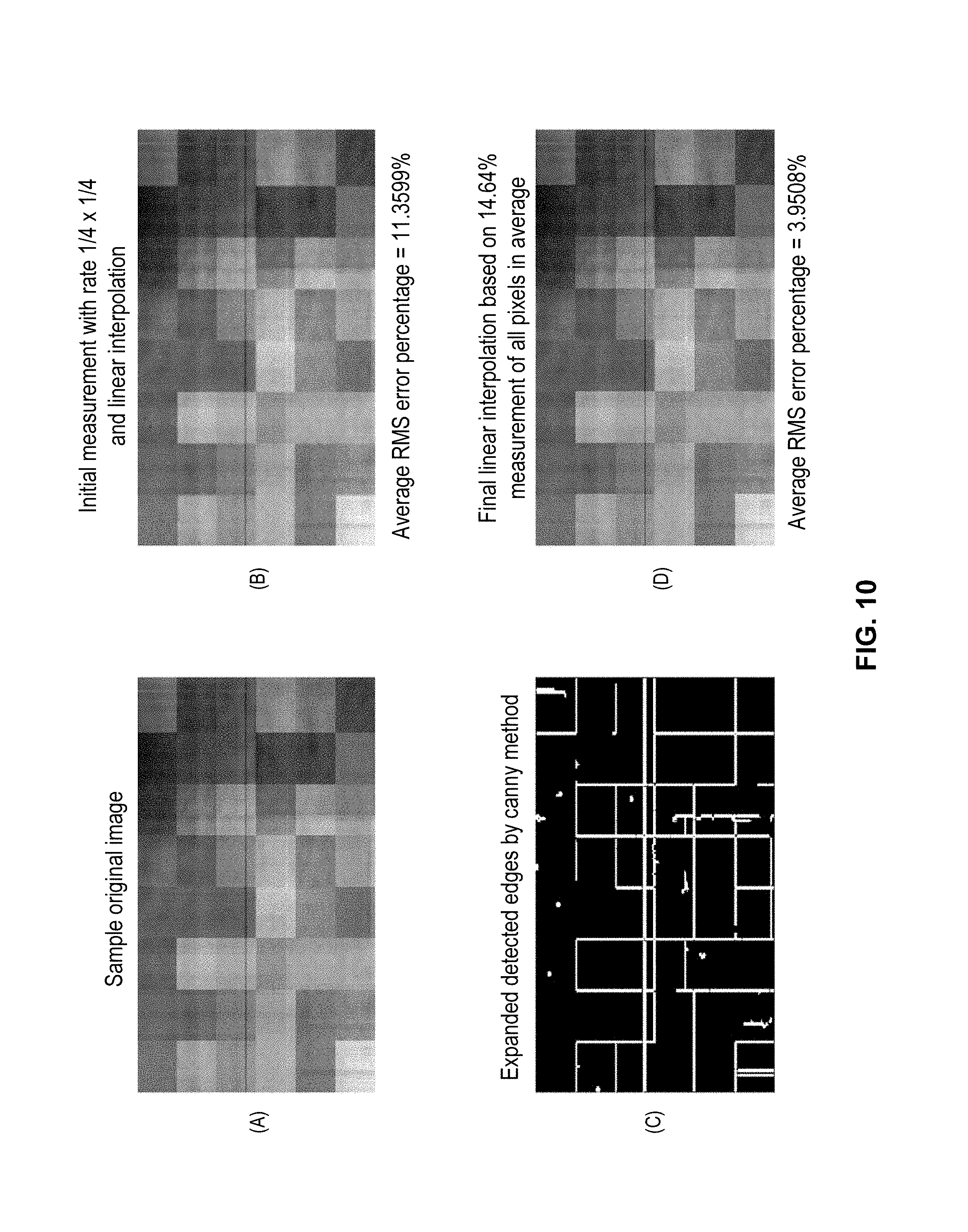
FIG. 10 shows the performance of the algorithm on the random intensity chess pattern with background real initial non-uniformity for green color.
FIG. 11 shows the performance of the algorithm on the random intensity chess pattern with background real initial non-uniformity for blue color.
FIG. 12 shows the performance of the algorithm on the random intensity diamond pattern with the background of real initial non-uniformity for red color.
FIG. 13 shows the performance of the algorithm on the random intensity diamond pattern with the background of real initial non-uniformity for green color.
FIG. 14 shows the performance of the algorithm on the random intensity diamond pattern with the background of real initial non-uniformity for blue color.
While the present disclosure is susceptible to various modifications and alternative forms, specific embodiments have been shown by way of example in the drawings and will be described in detail herein. It should be understood, however, that the disclosure is not intended to be limited to the particular forms disclosed. Rather, the disclosure is to cover all modifications, equivalents, and alternatives falling within the spirit and scope of the invention as defined by the appended claims.
DETAILED DESCRIPTION
While particular embodiments and applications of the present disclosure have been illustrated and described, it is to be understood that the disclosure is not limited to the precise construction and compositions disclosed herein and that various modifications, changes, and variations can be apparent from the foregoing descriptions without departing from the spirit and scope of the invention as defined in the appended claims.
The aging pattern of a screen or display is highly spatially correlated. For displays having low correlated or uncorrelated aging patterns, most or even all of the pixels need to be measured to ascertain their aging characteristic. However, due to high spatial correlation, the aging pattern of the display can be estimated from measuring a proper subset of all pixels in the display. The present disclosure presents a class of approaches that are based on pixel measurement. An algorithm which is easy to implement and works based on measuring a non-uniform subset of pixels to estimate the aging pattern of the display is presented.
Referring to FIG. 1, an algorithm starts with an initial uniform (by uniform, it is meant that a regular or uniform pattern of pixels are measured) measurement of a characteristic (e.g., aging) of the pixels with a specific down-sampling rate K.sub.V.times.K.sub.H, such as for example 4.times.4, which means that the aging characteristic of the pixel in every 4.sup.th row and every 4.sup.th column is measured while other pixels in each 4.times.4 block of pixels are not measured in this initial uniform measurement of the algorithm 100 (102). Assuming a high spatial correlation, a coarse aging pattern of the entire display (including non-measured pixels) is obtained by interpolating the measured data (104). Most of the error due to interpolation can happen at or near the vicinity of the edges where image brightness levels change abruptly. Accordingly, an edge detection algorithm is run to detect the edges where sudden brightness levels occur (106). Then, the aging pattern is further refined by making extra pixel measurements at or around the detected edges (108) and then re-interpolating the measured aging data across the entire display (110).
An initial pixel measurement is performed with the down-sampling rate of K.sub.V.times.K.sub.H. Starting from a corner of the display (e.g., the upper-left corner) with the coordinate (0,0), the pixels located at integer multiples (e.g., 4) of the vertical and horizontal parameters of the down-sampling rate are measured. Depending on the size of the display and the selected down-sampling rate, a few last rows (n.sub.r<K.sub.V) and a few last columns (n.sub.c<K.sub.H) of the pixels may not be measured during this initial pixel measurement using the selected down-sampling rate. Prior to interpolating for all the pixels of the display, aging characteristics of the pixels at the very last row and the very last column of the display are measured with the same down-sampling rates K.sub.H and K.sub.V, respectively. The pixel at the location corresponding to the bottom right of the display (N.sub.r, N.sub.c) can also be measured as part of the initial measurement. The aging characteristics of the measured pixels are stored as a set of initial pixel measurements in a memory device. The parameters of the down-sampling rate, K.sub.V and K.sub.H, are integers and can be identical (e.g., 2.times.2 or 4.times.4) or mutually distinct (e.g., 2.times.4).
Depending on the size of the display and the selected down-sampling rate K.sub.V.times.K.sub.H, the display can be (at most) divided to four disjoint (distinct) regions to which the initial uniform measurement is applied. This is due to the fact that the coordinates of the last row and the last column of pixels may not be integer factors of the selected down-sampling rate, and, so they can be measured separately. If the measurement is started from the upper-left corner of the screen, for example, these regions are located at the upper left, lower left, upper right, and the lower right parts of the display, respectively. In each region, a gridded interpolation algorithm is run to estimate the unknown entries of the matrix X, which again has a size corresponding to the pixel resolution of the display and where the known entries correspond to the measured characteristics, and the unknown entries are interpolated.
Various conventional methods of interpolation such as "nearest neighbor," "linear," "cubic," or "spline" can be used. In case that cubic or spline interpolation methods are deployed, the interpolated data in region 1 can be used to provide extra data needed to complete interpolation in regions 2 and 3. Similarly, the interpolated data in regions 1, 2, and 3 can be used to complete the interpolation in region 4. Alternatively, the pixels required for interpolation at regions 2, 3, 4 can be directly measured.
Because edges happen due to abrupt changes in the intensity or brightness of surrounding pixels, they can result in local maximums in the gradient magnitude of the image. This phenomenon allows detection of the edges using image signal processing by finding the local maximums of the gradient of the image. Conventional edge detection algorithms such as "sobel," "prewitt," "log," and "roberts" work according to this principle, and are suitable for use in detecting the local maximums of the image gradient.
A more advanced edge detection algorithm which works based on finding and tracking the local maximums of the gradient is a "canny" edge detector which was developed by John F. Canny in 1986. The canny edge detector can be used herein due to its precise detection and location of connected edges and accordingly more precise recognition of different aged areas of the display.
The output of the canny edge detector is a binary matrix with the same size of the original image (i.e., the same size as matrix X) in which the edge entries (e.g., local maxima) are marked by a binary value of one and the rest of the entries in the binary matrix are zero.
Assuming that the canny edge detector finds the location of the edges precisely, the location of each edge can still have an error of at most K.sub.V.times.K.sub.H pixels due to the down-sampling resolution of the initial interpolation. Three different approaches can be used to reduce the error.
A coarse or "brute force" approach is to measure all (K.sub.V+1).times.(K.sub.H+1) pixels between the four initial measurements around the detected edge. When the edge is placed on an initially measured pixel, the (K.sub.V+1).times.(K.sub.H+1) pixels horizontally on the right and vertically below the current pixel (starting from the edge pixel itself) are measured. For example if K.sub.V=K.sub.H=4, there are 25 pixels around the edge pixel that need to be measured. Because four of them have already been measured during the initial measurement (and are already in the set of initial pixel measurements), a total of at most 21 pixels around the detected edge pixel are measured. However, this approach can result in too many new pixels being measured without a material reduction of error.
To reduce the number of additional measurements, another approach measures a total of (K.sub.H+1) horizontal and (K.sub.V+1) vertical pixels around the detected edge and between the coordinates of the adjacent initially measured pixels. When the edge is placed on an initially measured pixel, the (K.sub.H+1) horizontal and the (K.sub.V+1) vertical pixels on the right of the edge pixel and below the edge pixel (including itself) is measured. Assuming K.sub.H=K.sub.V=4, a total of at most 10 pixels around the edge pixel are measured using this approach.
To further reduce the number of additional measurements, yet another approach measures a total of at most (K.sub.H+1) pixels on the right of the edge pixel and a total of at most (K.sub.V+1) vertical pixels below and including the edge pixel. The measurement can be stopped when the coordinates of a next initially measured pixel are reached. In this approach, at most (Kh+1) pixels horizontally and (K.sub.V+1) pixels vertically are measured.
Note that in all the above approaches, the new pixels that are measured can overlap with previously measured pixels due to the initial measurement or due to the extra measurement for other pixels at edges. These new pixels are skipped as they have already been measured. The additional pixels that are measured following the initial interpolation produce a set of edge measurements.
The new set of measured data now includes the initial pixel measurements (set of initial pixel measurements) plus the new measurements at the edges and their vicinity (set of edge measurements). This new data set is not a gridded set of data because the edges do not necessarily follow a gridded pattern. Thus, a scattered data interpolation technique is used to interpolate this new data set having an irregular or non-grid pattern of measured data. The re-interpolation using a scattered data interpolation results in a more accurate estimation of the aging pattern with less error compared to the initial interpolation alone.
The performance of the algorithm is evaluated for both simulated and real data of an AMOLED display. The normalized root mean square (RMS) error percentage is considered as the performance criterion. If X and {circumflex over (X)} are respectively the original and the estimated matrices, the normalized error can be defined as:
.times..DELTA..times..function..function..times. ##EQU00001##
It is assumed that the average value of the entries of matrix X is zero, otherwise it is taken off from every single entry of the matrix X. This is necessary to highlight the estimation error. Otherwise, the more is the average value, the less is the estimation error.
Four different simulated aging patterns respectively called "chess," "random intensity chess," "diamond," and "random intensity diamond" can be considered. The goal is twofold at this stage: 1) to determine a minimum number of measurements for a fixed pattern to achieve a reasonable estimation error, and 2) to observe the minimum size of the aged areas on the display in which the algorithm still shows a desirable performance. The simulated patterns can be added to a background of real data acquired from an AMOLED display. The performance of the algorithm is also evaluated in this case
FIG. 2(A) shows a simulated chess aging pattern having a size 6.times.10 (black and white blocks) across a display having a size of 384.times.648 pixels. The size of each block in this example is 64.times.64 pixels. The initial pixel measurement is performed with the down-sampling rate of 4.times.4. FIG. 2(B) shows an image obtained by a linear interpolation of the measured data using the down-sampling rate. The normalized RMS estimation error is 23.1039%. FIG. 2(C) shows the edges detected by a canny edge detector. Note that the edges can be expanded as explained before to cover their vicinity. FIG. 2(D) illustrates the re-interpolated image in which new data at and/or near the detected edges are taken into account. The normalized RMS error improves to 1.0551% but at a cost of measuring 17.99% of all the pixels on the display.
In another example, the initial pixel measurement is performed with the down-sampling rate of 2.times.3. In this example, more than 16.6% of all pixels are measured uniformly. This value is comparable with the obtained from the previous example as the total percentage of the pixel measurements, 17.99% value. The initial interpolation in this example results in a normalized RMS error of 14.9986%. This indicates that the algorithm results in more than a 13% improvement in the normalized RMS error compared to the case in which almost the same number of pixels is measured uniformly across the display.
FIG. 3 shows the results of the same simulation with a chess aging pattern of size 24.times.40. In this example, the size of each block is 16.times.16 pixels. Notice that the RMS error percentage after the initial interpolation is 50.3224%. It improves to 2.1963% following Canny edge detection and re-interpolation. This gain is achieved at a cost of measuring 51.26% of all pixels. Consistent with the previous simulation, it is seen that if the initial down-sampling rate were chosen as 2.times.1, i.e., when more than half of the pixels are measured uniformly, the RMS error percentage improves to 24.5427%. This translates to achieving more than a 22% performance improvement, which is due to an intelligent choice of pixels that are measured. As can be seen, the algorithm performs very well even for a very small size of aged areas (e.g., as small as 16.times.16 pixels).
In random intensity chess pattern each of the blocks chooses a random intensity level from the set {0, 0.1, 0.2, . . . , 1}. FIG. 4 illustrates the performance of the algorithm for an instant of this pattern of size 6.times.10 blocks. The simulation procedure is the same as that of the chess pattern. Note that the average RMS error and the average percentage of the total pixel measurement have been shown on the figure. These values were obtained based on 50 independent runs of the algorithm. As can be seen, the final average estimation error is 1.9744%, which is obtained at the cost of 15% average measurement of all pixels. In contrast, if the original image is sampled with the down-sampling rate of 2.times.3 and is linearly interpolated, the average RMS error equal to 12.29% is achieved. Thus, the algorithm provides more than 10% gain in average compared to a uniform measurement of pixels.
FIG. 5 illustrates the results of the same simulation when a random intensity chess pattern of size 24.times.40 is considered. The final average RMS error is 4.6394%, which is obtained at the cost of 40.79% average measurement of all pixels. By contrast, if the original image is sampled by the down-sampling rate of 2.times.1 and is interpolated, the average RMS error is 19.3118%. Thus, the algorithm provides more than 14% gain compared to the uniform measurement of pixels. The algorithm also performs very well even for very small size of aged areas (as small as 16.times.16 pixels). Table 1 summarizes the results for the chess and the random intensity chess aging patterns.
TABLE-US-00001 TABLE 1 Performance of the algorithm for simulated aging patterns Random Int. Random Int. Chess Chess Diamond diamond Pattern size 6 .times. 10 6 .times. 10 6 .times. 10 6 .times. 10 Initial down- 4 .times. 4 4 .times. 4 4 .times. 4 4 .times. 4 sampling rate Initial RMS error % 23.1 19.1 11.1 10.1 Total pixel 18 15 25.03 21.33 measurement % Final RMS error % 1.06 1.97 1.23 1.3 Equivalent down- 2 .times. 3 2 .times. 3 2 .times. 2 2 .times. 2 sampling rate Equivalent RMS 15 12.29 8.23 7.50 error % Gain % >13 >10 >7 >6
To verify the performance of the algorithm for edges with 45 and 135 edge direction degrees, a diamond aging pattern and the random intensity diamond pattern is designed as shown in FIGS. 6 and 7. The same simulation procedure as before is performed for both cases. In FIG. 6, the final RMS error is 1.2276%, which is obtained at the cost of 25.03% measurement of all pixels. For comparison, if the initial down-sampling rate equal to 2.times.2 is chosen, the RMS percentage error equal to 8.2349% is obtained. Thus, the algorithm provides more than 7% improvement in comparison to a uniform measurement of the pixels.
The algorithm was run 50 times for the random intensity diamond pattern and the results were averaged. The averaged final estimation error is 1.2986%, which is obtained at the cost of 21.33% percent measurement of all pixels on average. If the display is initially sampled with the down-sampling rate of 2.times.2 and the resulted data is linearly interpolated, the average RMS error is 7.5091%. Thus, the algorithm results in more than 6% improvement compared to a uniform pixel measurement approach. Table 1 above summarizes the results for the diamond and the random intensity diamond aging patterns.
In the following section, the random intensity chess and the random intensity diamond aging patterns are considered on a background of initial non-uniformity measured from an AMOLED display of size 512.times.648 pixels. FIG. 8 illustrates the V.sub.T initial non-uniformity of this display for Red, Green, and Blue colors. In these images, those values that are away from the mean (m) more than 10 times the standard deviation (.sigma.) are considered as false measurements and are replaced by the mean value. Those that are away from the mean 5 times the standard deviation are replaced by the boundary values, m.+-.5.sigma.. Then the data is filtered out by the 3.times.3 Gaussian filter to reduce the effect of the noise and to avoid pixel-by-pixel variation.
FIGS. 9, 10, and 11 show the performance of the algorithm for a random intensity chess pattern of size 6.times.10 with a background having real initial non-uniformity for red, green, and blue colors, respectively. The maximum intensity of the random chess pattern that is added to the initial non-uniformity data is 0.1 times the mean of the initial non-uniformity of the display. This means that the aging process is in an early stage, and the display is at most 10% aged compared to its original condition. The average RMS errors equal to 9, 3.95, and 2.43 percent are obtained at the cost of total 17.12, 14.64, and 17.62 percent measurement of all pixels on average respectively for red, green, and blue colors. To obtain the actual value of the performance improvement for each color, initial measurements of the display with a down-sampling rate of 2.times.3 were taken, which means that more than 16.6% of the pixels are measured uniformly. In this case, the average RMS errors equal to 14.7, 10.64, and 3.58 percent are obtained respectively for red, green, and blue colors. This translates to more than 5%, 6%, and 1% performance improvement respectively. The results are summarized in Table 2 below.
FIGS. 12-14 show the performance of the algorithm for a random intensity diamond pattern with a background having real initial non-uniformity respectively for red, green, and blue colors. Like previous simulations, the maximum intensity of the random diamond pattern that is added to the initial non-uniformity data is 0.1 times the mean of the initial non-uniformity of the display. Thus, the aging process is in an early stage, and the display is at most 10% aged compared to its original condition. The average RMS errors equal to 8.2, 3.5, and 2.65 percent are obtained at the cost of total 21.52, 17.76, and 19.01 percent measurement of all pixels on average respectively for red, green, and blue colors.
To obtain the actual value of the performance improvement for each color, two different scenarios of uniform pixel measurement are considered, and the average of the results is taken. In the first scenario, the pixels are uniformly measured with the down-sampling rate equal to 2.times.2. This means that more than 25% of the pixels are initially measured. Note that this number is much larger than the number of pixels measured using the algorithm for each color. The average RMS errors equal to 10, 7.24, and 2.34 percent are obtained respectively for red, green, and blue colors. Even in this scenario, the algorithm provides more than 1.8 and 3.5 percent gain for the red and green colors. The results for the blue color are very close. In another scenario, the initial down-sampling rate of 2.times.3 is chosen, which means that more than 16.6% of the pixels are measured. The averaged RMS errors of 14.15, 9.97, and 3.24 percent are obtained respectively for red, green, and blue colors. By taking the average of the results in both scenarios, the algorithm herein provides more than 3.9, 5.1, and 0.15 percent gain for red, green and blue colors compared to a strictly uniform pixel measurement approach. The results are summarized in Table 2.
TABLE-US-00002 TABLE 2 Performance of the algorithm for the simulated aging patterns with a background of real initial non-uniformity Random Random Intensity Chess Intensity diamond R G B R G B Pattern size 6 .times. 8 6 .times. 8 Initial down- 4 .times. 4 4 .times. 4 sampling rate Initial RMS error 15.57 11.36 4.83 15.27 10.25 3.93 Total Pixel 17.12 14.64 17.62 21.52 17.76 19.01 measurement % Final RMS 9.02 3.95 2.43 8.22 3.53 2.65 error % Equivalent down- 2 .times. 3 2 .times. 2, sampling rate 2 .times. 3 Equivalent RMS 14.4 10.64 3.58 12.25 8.6 2.8 error % Gain % >5 >6 >1 >3.9 >5.1 >0.15
The performance of the algorithm improves as the aging becomes more severe. In such a case, the edges are sharper and hence more vulnerable to be detected. In addition, assuming highly spatially correlated aged areas, most of the estimation error due to interpolation happen at the edges and their vicinity. Thus, pixel measurement at edges is more effective to reduce the estimation error. In general, the algorithm shows its best performance when it deals with highly spatially correlated areas with distinctive edges.
The algorithm herein includes an initial uniform pixel measurement and interpolation followed by an edge detection algorithm to recognize the areas that results in most part of the estimation error due to the interpolation. The pixels on the edges and their vicinity are also measured and aging pattern of the display is obtain by re-interpolation of the entire measured set of data for the initially measured pixels and the pixels around the detected edges. Numerical results on simulated aging patterns and real data demonstrate that the algorithm significantly outperforms the equivalent uniform pixel measurement counterpart. The algorithm performs particularly well for aging patterns that consist of highly spatially correlated areas with distinctive edges.
The simulation results presented here for real data are obtained based on only one set of real V.sub.T initial non-uniformity. More exact results are obtained by performing the same simulation for various sets of real data and averaging over the results.
There is a tradeoff in the choice of the initial down-sampling rate. It should be large enough to decrease the total number of pixel measurements as much as possible. At the same time, it should be small enough to capture important events (e.g., edges or corner points) of the image with a high probability. Clearly, if an edge is missed in the initial interpolation, it is not guaranteed to be recovered by the algorithm. Thus, edges that are expanded in an area smaller than the smallest area characterized by the down-sampling rate (K.sub.V.times.K.sub.H pixels), are vulnerable to be missed.
* * * * *
References
D00000
D00001
D00002
D00003
D00004
D00005
D00006
D00007
D00008
D00009
D00010
D00011
D00012

D00013

D00014

M00001

XML
uspto.report is an independent third-party trademark research tool that is not affiliated, endorsed, or sponsored by the United States Patent and Trademark Office (USPTO) or any other governmental organization. The information provided by uspto.report is based on publicly available data at the time of writing and is intended for informational purposes only.
While we strive to provide accurate and up-to-date information, we do not guarantee the accuracy, completeness, reliability, or suitability of the information displayed on this site. The use of this site is at your own risk. Any reliance you place on such information is therefore strictly at your own risk.
All official trademark data, including owner information, should be verified by visiting the official USPTO website at www.uspto.gov. This site is not intended to replace professional legal advice and should not be used as a substitute for consulting with a legal professional who is knowledgeable about trademark law.