Display tile structure and tiled display
Bower , et al. Ja
U.S. patent number 10,181,507 [Application Number 15/644,570] was granted by the patent office on 2019-01-15 for display tile structure and tiled display. This patent grant is currently assigned to X-Celeprint Limited. The grantee listed for this patent is X-Celeprint Limited. Invention is credited to Christopher Bower, Ronald S. Cok, Matthew Meitl.


| United States Patent | 10,181,507 |
| Bower , et al. | January 15, 2019 |
Display tile structure and tiled display
Abstract
A display tile structure includes a tile layer with opposing emitter and backplane sides. A light emitter having first and second electrodes for conducting electrical current to cause the light emitter to emit light is disposed in the tile layer. First and second electrically conductive tile micro-wires and first and second conductive tile contact pads are electrically connected to the first and second tile micro-wires, respectively. The light emitter includes a plurality of semiconductor layers and the first and second electrodes are disposed on a common side of the semiconductor layers opposite the emitter side of the tile layer. The first and second tile micro-wires and first and second tile contact pads are disposed on the backplane side of the tile layer.
| Inventors: | Bower; Christopher (Raleigh, NC), Meitl; Matthew (Durham, NC), Cok; Ronald S. (Rochester, NY) | ||||||||||
|---|---|---|---|---|---|---|---|---|---|---|---|
| Applicant: |
|
||||||||||
| Assignee: | X-Celeprint Limited (Cork,
IE) |
||||||||||
| Family ID: | 57731017 | ||||||||||
| Appl. No.: | 15/644,570 | ||||||||||
| Filed: | July 7, 2017 |
Prior Publication Data
| Document Identifier | Publication Date | |
|---|---|---|
| US 20170309698 A1 | Oct 26, 2017 | |
Related U.S. Patent Documents
| Application Number | Filing Date | Patent Number | Issue Date | ||
|---|---|---|---|---|---|
| 14822866 | Aug 10, 2015 | 9741785 | |||
| Current U.S. Class: | 1/1 |
| Current CPC Class: | G06F 3/0416 (20130101); H01L 27/156 (20130101); H01L 51/529 (20130101); H01L 25/0753 (20130101); H01L 33/64 (20130101); H01L 27/3276 (20130101); H01L 33/58 (20130101); G06F 3/044 (20130101); G06F 3/04164 (20190501); H01L 27/3288 (20130101); H01L 27/3293 (20130101); H01L 51/56 (20130101); G06F 3/04166 (20190501); G06F 3/0412 (20130101); H01L 25/048 (20130101); H01L 33/62 (20130101); H01L 2933/0075 (20130101); G06F 3/042 (20130101); H01L 2933/0066 (20130101); H01L 2227/326 (20130101); G06F 2203/04104 (20130101); H01L 2224/18 (20130101) |
| Current International Class: | H01L 27/32 (20060101); G06F 3/041 (20060101); H01L 33/58 (20100101); H01L 33/62 (20100101); G06F 3/044 (20060101); H01L 51/56 (20060101); H01L 51/52 (20060101); H01L 33/64 (20100101); H01L 27/15 (20060101); H01L 25/075 (20060101); H01L 25/04 (20140101) |
References Cited [Referenced By]
U.S. Patent Documents
| 4322735 | March 1982 | Sadamasa et al. |
| 4330329 | May 1982 | Hayashi et al. |
| 4591659 | May 1986 | Leibowitz |
| 5173759 | December 1992 | Anzaki et al. |
| 5550066 | August 1996 | Tang et al. |
| 5563470 | October 1996 | Li |
| 5621555 | April 1997 | Park |
| 5625202 | April 1997 | Chai |
| 5629132 | May 1997 | Suzuki et al. |
| 5686790 | November 1997 | Curtin et al. |
| 5739800 | April 1998 | Lebby et al. |
| 5780933 | July 1998 | Ohmori et al. |
| 5815303 | September 1998 | Berlin |
| 5994722 | November 1999 | Averbeck et al. |
| 6025730 | February 2000 | Akram et al. |
| 6084579 | July 2000 | Hirano |
| 6087680 | July 2000 | Gramann et al. |
| 6142358 | November 2000 | Cohn et al. |
| 6143672 | November 2000 | Ngo et al. |
| 6169294 | January 2001 | Biing-Jye et al. |
| 6184477 | February 2001 | Tanahashi |
| 6278242 | August 2001 | Cok et al. |
| 6392292 | May 2002 | Morishita |
| 6392340 | May 2002 | Yoneda et al. |
| 6403985 | June 2002 | Fan et al. |
| 6410942 | June 2002 | Thibeault et al. |
| 6422716 | July 2002 | Henrici et al. |
| 6424028 | July 2002 | Dickinson |
| 6466281 | October 2002 | Huang et al. |
| 6504180 | January 2003 | Heremans et al. |
| 6577367 | June 2003 | Kim |
| 6660457 | December 2003 | Imai et al. |
| 6703780 | March 2004 | Shiang et al. |
| 6717560 | April 2004 | Cok et al. |
| 6756576 | June 2004 | McElroy et al. |
| 6812637 | November 2004 | Cok et al. |
| 6828724 | December 2004 | Burroughes |
| 6853411 | February 2005 | Freidhoff et al. |
| 6897855 | May 2005 | Matthies et al. |
| 6933532 | August 2005 | Arnold et al. |
| 6969624 | November 2005 | Iwafuchi et al. |
| 6975369 | December 2005 | Burkholder |
| 7009220 | March 2006 | Oohata |
| 7012382 | March 2006 | Cheang et al. |
| 7091523 | August 2006 | Cok et al. |
| 7098589 | August 2006 | Erchak et al. |
| 7127810 | October 2006 | Kasuga et al. |
| 7129457 | October 2006 | McElroy et al. |
| 7169652 | January 2007 | Kimura |
| 7195733 | March 2007 | Rogers et al. |
| 7259391 | August 2007 | Liu et al. |
| 7288753 | October 2007 | Cok |
| 7394194 | July 2008 | Cok |
| 7402951 | July 2008 | Cok |
| 7420221 | September 2008 | Nagai |
| 7466075 | December 2008 | Cok et al. |
| 7479731 | January 2009 | Udagawa |
| 7521292 | April 2009 | Rogers et al. |
| 7557367 | July 2009 | Rogers et al. |
| 7586497 | September 2009 | Boroson et al. |
| 7605053 | October 2009 | Couillard et al. |
| 7622367 | November 2009 | Nuzzo et al. |
| 7662545 | February 2010 | Nuzzo et al. |
| 7687812 | March 2010 | Louwsma et al. |
| 7704684 | April 2010 | Rogers et al. |
| 7791271 | September 2010 | Cok et al. |
| 7799699 | September 2010 | Nuzzo et al. |
| 7816856 | October 2010 | Cok et al. |
| 7834541 | November 2010 | Cok |
| 7893612 | February 2011 | Cok |
| 7919342 | April 2011 | Cok |
| 7927976 | April 2011 | Menard |
| 7932123 | April 2011 | Rogers et al. |
| 7943491 | May 2011 | Nuzzo et al. |
| 7969085 | June 2011 | Cok |
| 7972875 | July 2011 | Rogers et al. |
| 7982296 | July 2011 | Nuzzo et al. |
| 7990058 | August 2011 | Cok et al. |
| 7999454 | August 2011 | Winters et al. |
| 8029139 | October 2011 | Ellinger et al. |
| 8039847 | October 2011 | Nuzzo et al. |
| 8198621 | June 2012 | Rogers et al. |
| 8207547 | June 2012 | Lin |
| 8243027 | August 2012 | Hotelling et al. |
| 8261660 | September 2012 | Menard |
| 8288843 | October 2012 | Kojima et al. |
| 8334545 | December 2012 | Levermore et al. |
| 8394706 | March 2013 | Nuzzo et al. |
| 8440546 | May 2013 | Nuzzo et al. |
| 8450927 | May 2013 | Lenk et al. |
| 8470701 | June 2013 | Rogers et al. |
| 8502192 | August 2013 | Kwak et al. |
| 8506867 | August 2013 | Menard |
| 8531642 | September 2013 | Kiryuschev et al. |
| 8664699 | March 2014 | Nuzzo et al. |
| 8686447 | April 2014 | Tomoda et al. |
| 8722458 | May 2014 | Rogers et al. |
| 8735932 | May 2014 | Kim et al. |
| 8754396 | June 2014 | Rogers et al. |
| 8766970 | July 2014 | Chien et al. |
| 8791474 | July 2014 | Bibl et al. |
| 8794501 | August 2014 | Bibl et al. |
| 8803857 | August 2014 | Cok |
| 8817369 | August 2014 | Daiku |
| 8835940 | September 2014 | Hu et al. |
| 8854294 | October 2014 | Sakariya |
| 8860051 | October 2014 | Fellows et al. |
| 8877648 | November 2014 | Bower et al. |
| 8884844 | November 2014 | Yang et al. |
| 8889485 | November 2014 | Bower |
| 8895406 | November 2014 | Rogers et al. |
| 8902152 | December 2014 | Bai et al. |
| 8946760 | February 2015 | Kim |
| 8987765 | March 2015 | Bibl et al. |
| 9105813 | August 2015 | Chang |
| 9142468 | September 2015 | Bower et al. |
| 9153171 | October 2015 | Sakariya et al. |
| 9178123 | November 2015 | Sakariya et al. |
| 9202996 | December 2015 | Orsley et al. |
| 9308649 | April 2016 | Golda et al. |
| 9355854 | May 2016 | Meitl et al. |
| 9368683 | June 2016 | Meitl et al. |
| 9437782 | September 2016 | Bower et al. |
| 9444015 | September 2016 | Bower et al. |
| 9496155 | November 2016 | Menard et al. |
| 9520537 | December 2016 | Bower et al. |
| 9537069 | January 2017 | Bower et al. |
| 9555644 | January 2017 | Rogers et al. |
| 9626908 | April 2017 | Sakariya et al. |
| 9761754 | September 2017 | Bower et al. |
| 9899329 | February 2018 | Bower |
| 9899465 | February 2018 | Bower et al. |
| 2001/0022564 | September 2001 | Youngquist et al. |
| 2002/0096994 | July 2002 | Iwafuchi et al. |
| 2003/0211649 | November 2003 | Hirai et al. |
| 2004/0180476 | September 2004 | Kazlas et al. |
| 2004/0212296 | October 2004 | Nakamura et al. |
| 2004/0227704 | November 2004 | Wang et al. |
| 2004/0252933 | December 2004 | Sylvester et al. |
| 2005/0006657 | January 2005 | Terashita |
| 2005/0012076 | January 2005 | Morioka |
| 2005/0116324 | June 2005 | Yamaguchi |
| 2005/0116621 | June 2005 | Bellmann et al. |
| 2005/0140275 | June 2005 | Park |
| 2005/0168987 | August 2005 | Tamaoki et al. |
| 2005/0202595 | September 2005 | Yonehara et al. |
| 2005/0264472 | December 2005 | Rast |
| 2005/0275615 | December 2005 | Kahen et al. |
| 2005/0285246 | December 2005 | Haba et al. |
| 2006/0051900 | March 2006 | Shizuno |
| 2006/0055864 | March 2006 | Matsumura et al. |
| 2006/0063309 | March 2006 | Sugiyama et al. |
| 2006/0116046 | June 2006 | Morley et al. |
| 2007/0035340 | February 2007 | Kimura |
| 2007/0077349 | April 2007 | Newman et al. |
| 2007/0201056 | August 2007 | Cok et al. |
| 2007/0235849 | October 2007 | Othieno et al. |
| 2008/0006843 | January 2008 | Dai et al. |
| 2008/0211734 | September 2008 | Huitema et al. |
| 2008/0224153 | September 2008 | Tomoda |
| 2008/0224254 | September 2008 | Couillard et al. |
| 2009/0053498 | February 2009 | Matsuura et al. |
| 2009/0278141 | November 2009 | Coe-Sullivan et al. |
| 2009/0278142 | November 2009 | Watanabe et al. |
| 2009/0315054 | December 2009 | Kim et al. |
| 2010/0060553 | March 2010 | Zimmerman et al. |
| 2010/0078670 | April 2010 | Kim et al. |
| 2010/0123134 | May 2010 | Nagata |
| 2010/0123268 | May 2010 | Menard |
| 2010/0148198 | June 2010 | Sugizaki et al. |
| 2010/0186883 | July 2010 | Tomoda |
| 2010/0190293 | July 2010 | Maeda et al. |
| 2010/0207852 | August 2010 | Cok |
| 2010/0214247 | August 2010 | Tang et al. |
| 2010/0248484 | September 2010 | Bower et al. |
| 2010/0258710 | October 2010 | Wiese et al. |
| 2010/0264816 | October 2010 | Cok |
| 2010/0289115 | November 2010 | Akiyama et al. |
| 2010/0317132 | December 2010 | Rogers et al. |
| 2011/0043435 | February 2011 | Hebenstreit et al. |
| 2011/0067911 | March 2011 | Ishikawa et al. |
| 2011/0108800 | May 2011 | Pan |
| 2011/0133324 | June 2011 | Fan et al. |
| 2011/0147715 | June 2011 | Rogers et al. |
| 2011/0211348 | September 2011 | Kim |
| 2012/0009738 | January 2012 | Crawford et al. |
| 2012/0080692 | April 2012 | Ohtorii |
| 2012/0119249 | May 2012 | Kim et al. |
| 2012/0141799 | June 2012 | Kub et al. |
| 2012/0223636 | September 2012 | Shin et al. |
| 2012/0223875 | September 2012 | Lau et al. |
| 2012/0228669 | September 2012 | Bower et al. |
| 2012/0256163 | October 2012 | Yoon et al. |
| 2012/0313241 | December 2012 | Bower |
| 2012/0314388 | December 2012 | Bower et al. |
| 2012/0319563 | December 2012 | Ishihara |
| 2013/0015483 | January 2013 | Shimokawa et al. |
| 2013/0036928 | February 2013 | Rogers et al. |
| 2013/0069275 | March 2013 | Menard et al. |
| 2013/0088416 | April 2013 | Smith et al. |
| 2013/0196474 | August 2013 | Meitl et al. |
| 2013/0207964 | August 2013 | Fleck et al. |
| 2013/0221355 | August 2013 | Bower et al. |
| 2013/0249138 | September 2013 | DeSimone et al. |
| 2013/0273695 | October 2013 | Menard et al. |
| 2013/0309792 | November 2013 | Tischler et al. |
| 2013/0333094 | December 2013 | Rogers et al. |
| 2014/0104243 | April 2014 | Sakariya et al. |
| 2014/0146273 | May 2014 | Kim et al. |
| 2014/0175498 | June 2014 | Lai |
| 2014/0183446 | July 2014 | Nago et al. |
| 2014/0217448 | August 2014 | Kim et al. |
| 2014/0231839 | August 2014 | Jeon et al. |
| 2014/0231851 | August 2014 | Tsai et al. |
| 2014/0264763 | September 2014 | Meitl et al. |
| 2014/0267683 | September 2014 | Bibl et al. |
| 2014/0306248 | October 2014 | Ahn et al. |
| 2014/0367633 | December 2014 | Bibl et al. |
| 2014/0367705 | December 2014 | Bibl et al. |
| 2015/0135525 | May 2015 | Bower |
| 2015/0137153 | May 2015 | Bibl et al. |
| 2015/0169011 | June 2015 | Bibl et al. |
| 2015/0263066 | September 2015 | Hu et al. |
| 2015/0280066 | October 2015 | Fujimura et al. |
| 2015/0280089 | October 2015 | Obata et al. |
| 2015/0371585 | December 2015 | Bower et al. |
| 2015/0371974 | December 2015 | Bower et al. |
| 2015/0372051 | December 2015 | Bower et al. |
| 2015/0372052 | December 2015 | Bower et al. |
| 2015/0372053 | December 2015 | Bower et al. |
| 2015/0372187 | December 2015 | Bower et al. |
| 2015/0373793 | December 2015 | Bower et al. |
| 2016/0005721 | January 2016 | Bower et al. |
| 2016/0018094 | January 2016 | Bower et al. |
| 2016/0064363 | March 2016 | Bower et al. |
| 2016/0066789 | March 2016 | Rogers et al. |
| 2016/0093600 | March 2016 | Bower et al. |
| 2016/0308103 | October 2016 | Hu et al. |
| 2017/0025593 | January 2017 | Bower et al. |
| 2017/0047393 | February 2017 | Bower et al. |
| 2017/0187976 | June 2017 | Cok |
| 2017/0206845 | July 2017 | Sakariya et al. |
| 2017/0210117 | July 2017 | Rogers et al. |
| 2017/0213803 | July 2017 | Bower |
| 2017/0250167 | August 2017 | Bower et al. |
| 2018/0130751 | May 2018 | Bower |
| 2018/0138071 | May 2018 | Bower et al. |
| 1548571 | Jun 2005 | EP | |||
| H11-142878 | May 1999 | JP | |||
| 2011/066130 | Mar 2011 | JP | |||
| WO-2006/027730 | Mar 2006 | WO | |||
| WO-2006/099741 | Sep 2006 | WO | |||
| WO-2008/103931 | Aug 2008 | WO | |||
| WO-2010/032603 | Mar 2010 | WO | |||
| WO-2010/102310 | Sep 2010 | WO | |||
| WO-2010/111601 | Sep 2010 | WO | |||
| WO-2010/132552 | Nov 2010 | WO | |||
| WO-2013/064800 | May 2013 | WO | |||
| WO-2014/121635 | Aug 2014 | WO | |||
| WO-2014/149864 | Sep 2014 | WO | |||
| WO-2016/046283 | Mar 2016 | WO | |||
| WO-2017/144573 | Aug 2017 | WO | |||
Other References
|
Chesterfield, R. J. et al., 63.3:Multinozzle Printing: A Cost-effective Process for OLED Display Fabrication, SID 2009 Digest, vol. XL:Book II, 951-954. cited by applicant . Choi, H. W. et al., Efficient GaN-based Micro-LED Arrays, Mat. Res. Soc. Symp. Proc. 743:L6.28.1-L6.28.6 (2003). cited by applicant . Hamer et al., 63.2: AMOLED Displays Using Transfer-Printed Integrated Circuits, SID 09 Digest, 40(2):947-950 (2009). cited by applicant . Lee, S. H. etal, Laser Lift-Offof GaN Thin Film and its Application to the Flexible Light Emitting Diodes, Proc. of SPIE 8460:846011-1-846011-6 (2012). cited by applicant . Ohno, Y. and Ohzeki, Y., Development of Ultrathin Bonding Wire for Fine Pitch Bonding, Nippon Steel Technical Report 59:1-5 (1993). cited by applicant . Poher, V. et al., Micro-LED arrays: a tool for two-dimensional neuron stimulation, J. Phys. D: Appl. Phys. 41:094014 (2008). cited by applicant . Roscher, H., VCSEL Arrays with Redundant Pixel Designs for 10Gbits/s 2-D Space-Parallel MMF Transmission, Annual Report, optoelectronics Department, (2005). cited by applicant . Yaniv et al., A 640 .times. 480 Pixel Computer Display Using Pin Diodes with Device Redundancy, 1988 International Display Research Conference, IEEE, CH-2678-1/88:152-154 (1988). cited by applicant. |
Primary Examiner: Alam; Mohammed R
Attorney, Agent or Firm: Haulbrook; William R. Schmitt; Michael D. Choate, Hall & Stewart
Parent Case Text
PRIORITY APPLICATION
This application is a divisional of U.S. patent application Ser. No. 14/822,866, filed on Aug. 10, 2015, the disclosure of which is hereby incorporated by reference herein in its entirety.
CROSS REFERENCE TO RELATED APPLICATIONS
Reference is made to commonly assigned U.S. patent application Ser. No. 14/807,259, filed Jul. 23, 2015 and entitled Redistribution Layer for Substrate Contacts by Bower et al, to commonly assigned U.S. patent application Ser. No. 14/743,984, filed Jun. 18, 2015 and entitled Systems and Methods for Preparing GaN and Related Materials for Micro Assembly by Bower et al, to commonly assigned U.S. patent application Ser. No. 14/807,311, filed Jul. 23, 2015 and entitled Printable Inorganic Semiconductor Method by Meitl et al, to commonly assigned U.S. patent application Ser. No. 14/818,201, filed Aug. 4, 2015 and entitled Inorganic-Light-Emitter Display with Integrated Black Matrix by Bower et al, to commonly assigned U.S. patent application Ser. No. 14/743,981, filed Jun. 18, 2015 and entitled Micro-Assembled Micro LED Displays and Lighting Elements by Bower et al, and to commonly assigned U.S. Patent Application Ser. No. 62/055,472 filed Sep. 25, 2014 and entitled Compound Micro-Assembly Strategies and Devices by Bower et al, the disclosures of which are incorporated herein by reference in their entirety.
Claims
The invention claimed is:
1. A method of making a display tile, comprising: providing a tile substrate having a structure side; disposing one or more light-emitting diodes (LEDs) on and in direct contact with the structure side of the tile substrate, each LED having a light-emitting side adjacent to the structure side to emit light through the tile substrate and an opposed connection side with first and second electrodes for providing electrical power to the LED to cause the LED to emit light; forming a tile layer on or over the one or more LEDs and structure side of the tile substrate and exposing the first and second electrodes, the tile layer having an emitter side adjacent to the structure side of the tile substrate and a backplane side opposite the emitter side, the tile layer including a layer of light-absorbing material disposed in the tile layer on and in direct contact with the tile substrate and only partially encapsulating the one or more LEDs; forming an electrically conductive first tile micro-wire electrically connected to the first electrode and an electrically conductive second tile micro-wire electrically connected to the second electrode, the first and second tile micro-wires disposed only on a side of the layer of light-absorbing material opposite the tile substrate and the first and second tile micro-wires not extending to the edges of the tile substrate; and forming an exposed conductive first tile contact pad electrically connected to the first tile micro-wire and an exposed conductive second tile contact pad electrically connected to the second tile micro-wire, wherein the one or more LEDs comprise a plurality of semiconductor layers and the first and second electrodes are disposed on a common side of the plurality of semiconductor layers opposite the emitter side of the tile layer and wherein the first and second tile micro-wires and first and second tile contact pads are disposed only on a side of the layer of light-absorbing material opposite the tile substrate on the backplane side of the tile layer, and the first and second tile contact pads disposed on a portion of the first and second tile micro-wires that are in contact with the layer of light-absorbing material.
2. The method of claim 1, comprising: providing a backplane having backplane contact pads on a backplane surface of the backplane; disposing the backplane side of the tile layer adjacent to the backplane surface so that the backplane contact pads are in correspondence with the first tile and second tile contact pads; and electrically connecting the tile contact pads to the backplane contact pads with electrical connectors.
3. The method of claim 2, comprising forming a tile heat-transfer structure on the tile layer, forming a backplane heat-transfer structure on the backplane, and thermally connecting the tile heat-transfer structure to the backplane heat-transfer structure.
4. The method of claim 2, comprising providing a plurality of display tiles electrically connected to the backplane to form a display.
5. The method of claim 2, comprising removing the tile substrate from the emitter side of the tile layer and from the one or more LEDs.
6. The method of claim 1, comprising providing a plurality of LEDs and cutting the tile layer into portions that each comprise respective one or more LEDs, respective first and second tile micro-wires, and respective first and second tile contact pads.
7. The method of claim 1, comprising forming the tile layer of a curable material, curing the curable material, and forming vias through at least a portion of the cured material to expose the first and second electrodes.
8. The method of claim 7, wherein the cured material is light absorbing, is a black matrix, comprises light-absorbing dyes, comprises light-absorbing pigments, or is black.
9. The method of claim 1, comprising disposing active or passive electrical components on or over the tile layer and electrically connecting the active or passive electrical components to the first and second tile micro-wires, the first and second tile contact pads, or the first and second electrodes.
10. The method of claim 1, comprising providing one or more active electrical components mounted on to the backplane side of the tile layer on a side of the layer of light-absorbing material opposite the tile substrate and electrically connected to the first or second tile micro-wires, electrodes, or tile contact pads and wherein at least one of the first or second tile micro-wires is electrically connected to the first tile contact pad or the second tile contact pad through one or more of the active electrical components.
11. The method of claim 10, wherein the active electrical components are transistors, integrated circuits, power supplies, or power-conversion circuits.
12. The method of claim 10, wherein at least one of the active electrical components is a driver that drives one or more of the LEDs.
13. The method of claim 1, comprising providing redundant red-light, green-light, and blue-light emitters arranged to emit light from the emitter side, the redundant red, green, and blue-light emitters each having respective first and second electrodes electrically connected to the first and second tile micro-wires, respectively.
14. The method of claim 1, wherein the one or more LEDs include a red-light emitter that emits red light, a green-light emitter that emits green light, and a blue-light emitter that emits blue light, each light emitter having the first and second electrodes electrically connected to the first and second tile micro-wires, respectively.
15. The method of claim 14, wherein the red, green, and blue light emitters form a full-color pixel in a display.
16. The method of claim 1, wherein the tile layer is a black matrix, comprises light-absorbing dyes, color-conversion materials, phosphors, single-crystal fluorophores, or nanocrystals, or comprises light-absorbing pigments, or is black.
17. The method of claim 1, comprising providing a transparent cover affixed to or coated on the emitter side of the tile layer.
18. The method of claim 1, wherein disposing the one or more LEDs on and in direct contact with the structure side of the tile substrate comprises micro-transfer printing the one or more LEDs onto the structure side of the tile substrate.
19. The method of claim 18, comprising providing the layer of light-absorbing material disposed in the tile layer on and in direct contact with the tile substrate and only partially encapsulating the one or more LEDs after micro-transfer printing the one or more LEDs.
20. The method of claim 18, comprising forming the first and second electrodes or first and second tile micro-wires after providing the layer of light-absorbing material.
Description
FIELD OF THE INVENTION
The present invention relates to a large-format display structure having pixel tiles located on a backplane forming a tiled display.
BACKGROUND OF THE INVENTION
Flat-panel displays are widely used in conjunction with computing devices, in portable devices, and for entertainment devices such as televisions. Such displays typically employ a plurality of pixels distributed over a display substrate to display images, graphics, or text. For example, liquid crystal displays (LCDs) employ liquid crystals to block or transmit light from a backlight behind the liquid crystals and organic light-emitting diode (OLED) displays rely on passing current through a layer of organic material that glows in response to the electrical current. Inorganic light-emitting diodes (LEDs) are also used in displays.
Most flat-panel displays use active-matrix thin-film transistors formed in a thin semiconductor layer on a substrate to control an array of light-emitting or light-controlling elements. However, the thin layer of semiconductor material is typically amorphous or has localized crystals, for example in amorphous silicon or polysilicon. These semiconductor material structures have a much lower performance than crystalline semiconductors found in typical integrated circuits. Moreover, it is difficult and expensive to make thin-film semiconductor structures on large substrates, limiting the size of integrated flat-panel devices such as displays. Passive-matrix control structures that do not require a thin-film semiconductor layer are also known but are limited in size resolution, and refresh rate.
At least in part because of these technical challenges, flat-panel displays were originally relatively small, for example having a display substrate diagonal measurement of only a few centimeters. As display substrate processing technology has improved, displays have increased in size, for example displays over three meters in diagonal have been demonstrated.
Large-format outdoor displays typically use inorganic light-emitting diodes (LEDs) individually mounted in a frame. In some displays, groups of LEDs are mounted in tiles and the tiles are assembled into the final display. If an LED in a tile fails, the faulty tile is removed and a good tile replaces the faulty tile. Moreover, tiles can be tested before assembly, increasing display yields. The use of tiles increases the available size of a display since each tile is separately made and is much smaller than the size of the display itself. However, it is in general challenging to provide electrical interconnections to the pixels in the tiles and to maintain a constant pixel pitch across the tile boundaries.
A variety of tiled display structures are known. U.S. Pat. No. 5,563,470 discloses a tiled panel display assembly with a common substrate on which a plurality of small display tiles are mounted in an array and electrically interconnected to form a large-area panel. Each tile includes a plurality of contact pads that are aligned with corresponding contact pads on the substrate. Solder joints between corresponding contact pads mechanically align and secure the tiles on the substrate and provide electrical connections therebetween. Selected substrate contact pads are electrically interconnected to provide electrical connections between adjacent tiles. Each of the tiles contains a plurality of metal-filled vias that connect contact pads on the under surfaces of the tiles to electrodes on the upper surface of the tile. Alternatively, electrical connections extend around the outer peripheral surface of the tile substrate. U.S. Pat. No. 8,531,642 shows a similar wrap-around electrical connection.
EP1548571 describes a configurable and scalable tiled OLED display. The OLED materials are deposited in a passive-matrix configuration on a transparent substrate and then interconnected with solder bump technology to a printed circuit board located on top of the transparent substrate. U.S. Pat. No. 6,897,855 describes a different tiled OLED structure with display tiles having picture element (pixel) positions defined up to the edge of the tiles. Each pixel position has an organic light-emitting diode (OLED) active area that occupies approximately 25 percent of the pixel area. Each tile includes a memory that stores display data, and pixel-driving circuitry that controls the scanning and illumination of the pixels on the tile. The pixel driving circuitry is located on the back side of the tile and connections to pixel electrodes on the front side of the tile are made by vias which pass through portions of selected ones of the pixel areas that are not occupied by the active pixel material. U.S. Pat. No. 6,897,855 also describes a tiled structure that employs vias through substrates to provide the electrical connections from the driving circuitry to the pixels on the display tiles, as does U.S. Pat. No. 6,853,411. U.S. Pat. No. 6,853,411 also describes locating pixel-driving circuitry beneath an OLED light emitter. Such a structure requires additional layers in a tile structure.
In an alternative arrangement, U.S. Pat. No. 7,394,194 describes a tiled OLED structure with electrical standoffs connecting OLED electrodes on a tile substrate with conductors on a back panel. The electrical standoffs are located on the edge of each tile to avoid compromising the environmental integrity of the OLED materials on the tile.
Inorganic light-emitting diode displays using micro-LEDs (for example having an area less than 100 microns square or having an area small enough that it is not visible to an unaided observer of the display at a designed viewing distance) are also known. For example, U.S. Pat. No. 8,722,458 entitled Optical Systems Fabricated by Printing-Based Assembly teaches transferring light-emitting, light-sensing, or light-collecting semiconductor elements from a wafer substrate to a destination substrate. U.S. Pat. No. 5,739,800 describes an LED display chip with an array of micro-LEDs mounted on a mounting substrate and electrically connected to a driver substrate. However, this arrangement requires multiple substrates and the use of vias to connect integrated circuits on the driver substrate to the LED display substrate and is not suitable for a scalable tiled structure.
Some displays use light-emitting structures on a backplane together with integrated circuits mounted on the backplane to provide control signals to the light-emitting structures. As discussed in U.S. Pat. No. 5,686,790, integrated circuits mounted on the light-emitting side of the backplane unnecessarily increase the size of the backplane while integrated circuits mounted on the side of the backplane opposite the light-emitting structures require electrical vias through the backplane or electrical leads wrapped around the edge of the backplane to electrically connect the integrated circuits with the light-emitting structures. Such vias and leads are difficult and expensive to construct. Integrated circuits located within the display area of a display reduce the resolution and aperture ratio of the display. In flat-panel displays such as LCDs and OLEDs, a reduced aperture ratio also reduces the brightness or lifetime of the display.
Multi-layer printed circuit boards (PCBs) are widely used in digital electronic systems to interconnect electronic elements such as integrated circuits and passive components such as resistors and capacitors. Such printed circuit boards include layers of insulating material interdigitated with patterned conductive layers such as etched copper sheets laminated with electrically conductive through-hole vias to interconnect the electronic elements, for example as disclosed in U.S. Pat. No. 4,591,659. However, these PCBs can be limited in the spatial resolution provided for integrated circuit electrical interconnections. Daughter cards used in conjunction with motherboards (i.e., smaller printed circuit boards mounted upon and electrically connected to larger printed circuit boards) are also known but likewise have limited spatial resolution, orientation, and integration provided for integrated circuits.
Thus there remains a need for a display tile structure that is simple to make and has increased brightness or lifetime in a robust structure for a tiled display.
SUMMARY OF THE INVENTION
The present invention provides display tile structures that can be integrated with a backplane to form a tiled display. According to embodiments of the present invention, the display tiles include inorganic light emitters, such as micro inorganic light-emitting diodes (LEDs) that are mounted to emit light in a direction opposite the backplane and that have electrodes, micro-wires, and contact pads on a side of the light emitters opposite the direction of light emission. This arrangement enables a tiled structure all of whose electrical connections are on a common side of the tile and adjacent to the backplane, so that no vias are needed through the tile layer and no wires are wrapped around the edges of the tile, thereby simplifying the structure and construction of display tiles and more readily enabling display tiles with a reduced perimeter width between the light emitters and the edge of the display tile that, in turn, can increase the resolution of the tiled display.
In contrast to the present invention, conventional inorganic LEDs, organic LEDs, and liquid crystal displays all require transparent electrodes through which light is emitted and which pass through or around the tile substrate to control the light emission, for example to provide power to the light-emitting material or liquid-crystal switching material.
In another embodiment of the invention, connections within a display tile area are enabled thereby increasing the density of the electrical interconnections to a display tile, reducing the minimum size of the display tiles, and enabling increased display resolution. Organic LEDs (OLEDs) require encapsulation layers for environmental protection that inhibit the use of connections within the display area and such interconnections obstruct light emission from the backlights of liquid crystal displays (LCDs). Furthermore, the use of small, bright emitters, for example micro-LEDs, enables a low-aperture ratio display, in contrast to OLED displays and LCDs, having increased area for interconnections between the light emitters as well as additional circuitry that enhances the functionality of the display tiles.
Furthermore, the present invention enables reduced-cost construction by providing tiles that are formed using very small components, for example micro-LEDs disposed on the tiles by micro-transfer printing, and small interconnections, for example made using photolithographic methods that enable a very high-resolution display that is then electrically connected to low-resolution contact pads electrically available to the backplane, which can then be constructed using a much lower resolution and less expensive technology, for example using parts, materials, and methods that are commonly used in printed circuit board manufacturing.
The present invention can also be made on a substrate that is subsequently removed, thereby forming a very thin structure that can be flexible. If the backplane is flexible, very large, flexible displays can be constructed.
In one aspect, the disclosed technology includes a display tile structure, the display tile structure including: a tile layer having a backplane side and an emitter side opposite the backplane side; a light emitter disposed in the tile layer and arranged to emit light from the emitter side, the light emitter having first and second electrodes for conducting electrical current to cause the light emitter to emit light; a first electrically conductive tile micro-wire electrically connected to the first electrode and a second electrically conductive tile micro-wire electrically connected to the second electrode; and a first conductive tile contact pad electrically connected to the first tile micro-wire and a second conductive tile contact pad electrically connected to the second tile micro-wire, wherein the light emitter comprises a plurality of semiconductor layers and the first and second electrodes are disposed on a common side of the semiconductor layers opposite the emitter side of the tile layer and wherein the first and second tile micro-wires and first and second tile contact pads are disposed on the backplane side of the tile layer.
In certain embodiments, the display tile structure includes a backplane having first and second backplane contact pads on a surface of the backplane and wherein the backplane side of the tile layer is adjacent to the backplane surface having the first and second backplane contact pads; and a first electrical connector electrically connecting the first tile contact pad to the first backplane contact pad and a second electrical connector electrically connecting the second tile contact pad to the second backplane contact pad.
In certain embodiments, the tile layer is a part of or forms a tile and the display tile structure includes a plurality of tiles with light emitters arranged in a regular array.
In certain embodiments, the display tile structure includes an index matching or light-absorbing layer located between the tile layers.
In certain embodiments, the tile layer comprises glass, a polymer, a curable polymer, sapphire, silicon carbide, metal, copper, or diamond.
In certain embodiments, the light emitter is an inorganic light emitting diode.
In certain embodiments, the light emitter is an inorganic light emitter having a light-emitting side and an opposed connection side adjacent to the backplane side of the tile layer and the first and second light-emitter electrodes are disposed on the connection side.
In certain embodiments, the first and second electrical connectors are metal interconnect structures, solder, solder balls, reflowed solder, anisotropic conductive films, or metal pillars.
In certain embodiments, the tiled layer is light absorbing, is a black matrix, comprises light-absorbing dyes, color-conversion materials, phosphors, single-crystal fluorophors, or nanocrystals, or comprises light-absorbing pigments, or is black.
In certain embodiments, the display tile structure includes a transparent cover affixed to or coated on the emitter side of the tile layer.
In certain embodiments, the first and second tile contact pads have a tile-contact-pad dimension over the tile layer, the first and second tile contact pads are spatially separated by a tile-contact-pad separation over the tile layer, the first and second micro-wires have a micro-wire width, the first and second electrodes have an electrode width, and the first and second electrodes are spatially separated by an electrode separation, wherein at least one of the following are true: the tile-contact-pad dimension is greater than the micro-wire width, the electrode width, or the electrode separation, or the tile-contact-pad separation is greater than the micro-wire width, the electrode width, or the electrode separation.
In certain embodiments, the backplane contact pads have a minimum dimension over the backplane that is greater than the tile-contact-pad dimension.
In certain embodiments, the display tile structure includes one or more passive electrical components mounted on to, formed on, or formed in the backplane side of the tile layer and electrically connected to the first or second micro-wires, electrodes, or contact pads.
In certain embodiments, the passive electrical components are resistors, capacitors, antennas, or inductors.
In certain embodiments, the display tile structure includes one or more active electrical components mounted on to the backplane side of the tile layer and electrically connected to the first or second micro-wires, electrodes, or contact pads.
In certain embodiments, the active electrical components are transistors, integrated circuits, power supplies, or power-conversion circuits.
In certain embodiments, at least one of the active electrical components is a driver that drives one or more of the light emitters.
In certain embodiments, the light-emitter is a red-light emitter that emits red light, and comprising a green-light emitter that emits green light and a blue-light emitter that emits blue light, each light emitter having first and second electrodes electrically connected to a tile micro-wire.
In certain embodiments, the display tile structure includes a plurality of light emitters in the tile layer.
In certain embodiments, the display tile structure includes redundant red-light, green-light, and blue-light emitters arranged to emit light from the emitter side, the redundant red, green, and blue-light emitters each light emitter having first and second electrodes electrically connected to a tile micro-wire.
In certain embodiments, the red, green, and blue light emitters form a full-color pixel in a display.
In certain embodiments, the display tile structure includes a plurality of tile contact pads spaced around the perimeter of the tile layer and at least one tile contact pad located within the interior of the tile layer.
In certain embodiments, the display tile structure includes one or more active electrical components mounted on to the backplane side of the tile layer and electrically connected to the tile contact pad located within the interior of the tile layer and wherein the plurality of tile contact pads spaced around the perimeter of the tile layer are connected to the light emitters.
In certain embodiments, the display tile structure includes a tile heat-transfer structure on or in the tile layer in thermal communication with a corresponding backplane heat-transfer structure on the backplane.
In certain embodiments, the thermal communication is a solder bond between the tile heat-transfer structure and the backplane heat-transfer structure.
In another aspect, the disclosed technology includes a tiled display including a plurality of display tile structures. The display includes a backplane having first and second backplane contact pads on a surface of the backplane and the backplane side of the tile layer is adjacent to the backplane surface having the first and second backplane contact pads; and a first electrical connector electrically connecting the first tile contact pad to the first backplane contact pad and a second electrical connector electrically connecting the second tile contact pad to the second backplane contact pad.
In another aspect, the disclosed technology includes a method of making a display tile, the method including: providing a substrate having a structure side; disposing one or more light emitters on the structure side of the substrate, each light emitter having a light-emitting side adjacent to the structure side to emit light through the substrate and an opposed connection side with electrodes for providing electrical power to the light emitter to cause the light emitter to emit light; forming a tile layer on or over the light emitters and structure side of the substrate and exposing the electrodes, the tile layer having an emitter side adjacent to the structure side of the substrate and a backplane side opposite the emitter side; forming tile micro-wires on or in the backplane side of the tile layer, the tile micro-wires electrically connected to the electrodes; and forming tile contact pads on or in the backplane side of the tile layer, the tile contact pads electrically connected to the tile micro-wires.
In certain embodiments, the method includes providing a backplane having backplane contact pads on a backplane surface of the backplane; disposing the backplane side of the tile layer adjacent to the backplane surface so that the backplane contact pads are in correspondence with the tile contact pads; and electrically connecting the tile contact pads to the backplane contact pads with electrical connectors.
In certain embodiments, the method includes forming a tile heat-transfer structure on the tile layer, forming a backplane heat-transfer structure on the backplane, and thermally connecting the tile heat-transfer structure to the backplane heat-transfer structure.
In certain embodiments, the method includes providing a plurality of display tiles electrically connected to the backplane to form a display.
In certain embodiments, the method includes removing the substrate from the emitter side of the tile layer and from the one or more light emitters.
In certain embodiments, the method includes providing a plurality of light emitters and cutting the tile layer into portions that each comprise one or more light emitters, tile micro-wires, and tile contact pads.
In certain embodiments, the method includes forming the tile layer of a curable materials, curing the material, and forming vias through at least a portion of the cured materials to expose the electrodes.
In certain embodiments, the cured material is light absorbing, is a black matrix, comprises light-absorbing dyes, comprises light-absorbing pigments, or is black.
In certain embodiments, the method includes disposing active or passive electrical components on or over the tile layer and electrically connecting electrical components to the tile micro-wires, tile contact pads, or electrodes.
The present invention provides a display tile structure and tiled display having increased resolution, reduced thickness, improved functionality, and reduced manufacturing cost.
BRIEF DESCRIPTION OF THE DRAWINGS
The foregoing and other objects, aspects, features, and advantages of the present disclosure will become more apparent and better understood by referring to the following description taken in conjunction with the accompanying drawings, in which:
FIG. 1 is a cross section of an embodiment of the present invention;
FIG. 2 is a detail cross section of a light emitter according to an embodiment of the present invention;
FIG. 3 is a cross section of an embodiment of the present invention including an electronic component;
FIG. 4 is a cross section of another embodiment of the present invention including a backplane;
FIG. 5 is a cross section of an embodiment of the present invention including redundant light emitters;
FIG. 6 is a plan view of an embodiment of the present invention including light emitters arranged in an array;
FIG. 7 is a cross section of another embodiment of the present invention including heat-spreading layers; and
FIGS. 8-9 are flow charts illustrating methods of the present invention.
The features and advantages of the present disclosure will become more apparent from the detailed description set forth below when taken in conjunction with the drawings, in which like reference characters identify corresponding elements throughout. In the drawings, like reference numbers generally indicate identical, functionally similar, and/or structurally similar elements. The figures are not drawn to scale since the variation in size of various elements in the Figures is too great to permit depiction to scale.
DETAILED DESCRIPTION OF THE INVENTION
Referring to the cross section of FIG. 1 and the detailed cross section of FIG. 2, in an embodiment of the present invention a display tile structure 5 includes a tile layer 30 having a backplane side 34 and an emitter side 32 opposite the backplane side 34. The tile layer 30 can include or be a light-absorbing material 36 and can include sub-layers such as a dielectric layer 37, particularly if the tile layer 30 is at least partially electrically conductive. The dielectric layer 37 can be an interlayer dielectric. A light emitter 20 is disposed in the tile layer 30 and arranged to emit light 97 from a light-emitting area 28 on the emitter side 32 of the tile layer 30. The light emitter 20 has first and second electrodes 22A, 22B, collectively referred to as electrodes 22, for conducting electrical current to cause the light emitter 20 to emit light 97. The first and second electrodes 22A, 22B can also be considered to be first and second light-emitter contact pads for the light emitter 20. The light emitter 20 can be a light-emitting diode, for example an inorganic light-emitting diode (LED) or a micro-LED.
A first electrically conductive tile micro-wire 40A is electrically connected to the first electrode 22A and a second electrically conductive tile micro-wire 40B is electrically connected to the second electrode 22B. A first electrically conductive tile contact pad 12A is electrically connected to the first tile micro-wire 40A and a second electrically conductive tile contact pad 12B is electrically connected to the second tile micro-wire 40B. The first and second tile micro-wires 40A and 40B are collectively referred to as tile micro-wires 40 and the first and second tile contact pads 12A and 12B are collectively referred to as tile contact pads 12. The first and second tile micro-wires 40A, 40B and the first and second tile contact pads 12A, 12B are disposed on the backplane side 34 of the tile layer 30 and, optionally, are electrically insulated from the light-absorbing material 36 and the light emitter 20 by the dielectric sub-layer 37. The first and second tile micro-wires 40A, 40B and the first and second tile contact pads 12A, 12B can be at least partially within the tile layer 30 as well as on or over the backplane side 34 of the tile layer 30. For example the electrodes 20 can be accessible through vias 38 that extend into and only partially through the tile layer 30. In certain embodiments, the first and second tile contact pads 12A, 12B must be accessible from the backplane side 34. In an embodiment, neither the tile micro-wires 40 nor the electrodes 22 are formed, located, or disposed on the emitter side 32 of the tile layer 30 so that no vias 38 through the tile layer 30 need be constructed. In particular, the tile layer 30 is at least partly between the tile micro-wires 40 and the emitter side 32 and at least partly between the tile contact pads 12 and the emitter side 32, so that ambient light 98 incident on the emitter side 32 of the tile layer 30 is at least partially absorbed and is at least partially not reflected from either of the tile contact pads 12 or the tile micro-wires 40.
Referring specifically to the detailed cross section of FIG. 2, in an embodiment of the present invention the light emitter 20 includes a plurality of semiconductor layers 21N, 21P, 21C (collectively semiconductor layers 21). The semiconductor layer 21N can be an n-doped semiconductor layer 21N, the semiconductor layer 21P can be a p-doped semiconductor layer 21P, and the semiconductor layer 21C can be a conductive semiconductor layer 21C optimized for transparency and conductivity and intended to conduct electrical current from the n- and p-doped semiconductor layers 21N, 21P to the second tile contact pad 12B through the second electrode 22B and second tile micro-wires 40B. The n-doped semiconductor layer 21N is electrically connected to the first tile contact pad 12A through the first electrode 22A and the first tile micro-wires 40A. The first and second electrodes 22A, 22B are disposed on a common side of the semiconductor layers 21 opposite the emitter side 32 and adjacent to the backplane side 34 of the tile layer 30. The electrodes 22 are electrically insulated from the semiconductor layers 21 by the dielectric layer 23 through which the vias 38 are formed to make electrical contact between the conductive semiconductor layer 21C and the n-doped semiconductor layer 21N. The light emitter 20 has a light-emitting side 24 coincident with the emitter side 32 of the tile layer 30 and a connection side 26 on which the first and second electrodes 22A, 22B are connected, although not necessarily in the same plane. The connection side 26 is adjacent to the backplane side 34 of the tile layer 30, although they are not necessarily coincident since the connection side 26 of the light emitter 20 can be partially covered with the light-absorbing material 36 of the tile layer 30. The first and second electrodes 22A, 22B are disposed on the connection side 26. In an embodiment, the light emitter 20 extends through, substantially through, mostly through, or at least partially through the tile layer 30. In an embodiment, the first and second tile micro-wires 40A, 40B and first and second tile contact pads 12A, 12B are disposed exclusively on the backplane side 34 of the tile layer 30.
In operation, an electrical voltage difference is provided across the tile contact pads 12 causing electrical current to flow through the tile micro-wires 40 and the electrodes 22 to the semiconductor layers 21N, 21P, 21C. Current flows through the n-doped semiconductor layer 21N and through the conductive semiconductor layer 21C to the p-doped semiconductor layer 21P where the electrons and holes combine to emit light from the light-emitting area 28 to emit light 97. Because the light-absorbing material 36 of the tile layer 30 absorbs ambient light 98 and because there are no reflective tile contact pads 12 or tile micro-wires 40 on the emitter side 32 of the tile layer 30, there is good contrast between the emitted light 97 and other ambient light 98.
The present invention, in certain embodiments, provides a display tile structure 5 without vias through the tile layer 30 and does not require transparent electrodes, for example indium tin oxide, through which light is emitted, and from which ambient light can be reflected. Transparent metal oxides, such as indium tin oxide, are not completely transparent, for example less than 90% transparent, and tend to be colored, for example yellow. Thus, by avoiding the use of such transparent conductors, the display tile structure 5 of the present invention increases light output and improves color. Furthermore by avoiding vias through the tile layer 30, costs and processing steps are reduced.
As shown in FIGS. 1 and 2, tile substrate 10 includes a substrate structure side 14 on which the display tile structure 5 can be disposed, constructed, or formed. In an embodiment, the display tile structure 5 is removably adhered or attached to the tile substrate 10.
Referring next to FIG. 3, the display tile structure 5 of the present invention, in certain embodiments, can include one or more electrical components 70 mounted or formed on or in the backplane side 34 of the tile layer 30 that are electrically connected to the tile micro-wires 40, electrodes 22, or tile contact pads 12. In one embodiment, the electrical components 70 are passive electrical components such as resistors, capacitors, antennas, or inductors. In another embodiment, the electrical components 70 include active electrical components such as transistors, integrated circuits, power supplies, or power-conversion circuits. In a further embodiment, at least one of the active electrical components 70 is a driver or controller that drives or controls one or more of the light emitters 20, for example an inorganic LED control circuit.
As shown in FIG. 3, the first and second tile contact pads 12 have a tile-contact-pad dimension D.sub.CP and are spatially separated by a tile-contact-pad separation S.sub.CP over the tile layer 30. The tile micro-wires 40 have a micro-wire width (not shown in the cross section of FIG. 3 but is the width of the tile micro-wires 40 over the tile layer 30). The electrodes 22 have an electrode width D.sub.E and are spatially separated by an electrode separation S.sub.E. In an embodiment, the tile-contact-pad dimension D.sub.CP is greater than the micro-wire width, the electrode width D.sub.E, or the electrode separation S.sub.E. Alternatively or in addition to, the tile-contact-pad separation S.sub.CP is greater than the micro-wire width, the electrode width D.sub.E, or the electrode separation S.sub.E. By constructing these elements within the sizes specified, shorts between the tile contact pads 12, tile micro-wires 40, or electrodes 22 are reduced and a lower-resolution patterning process can be used to form the display tile structure 5 of the present invention.
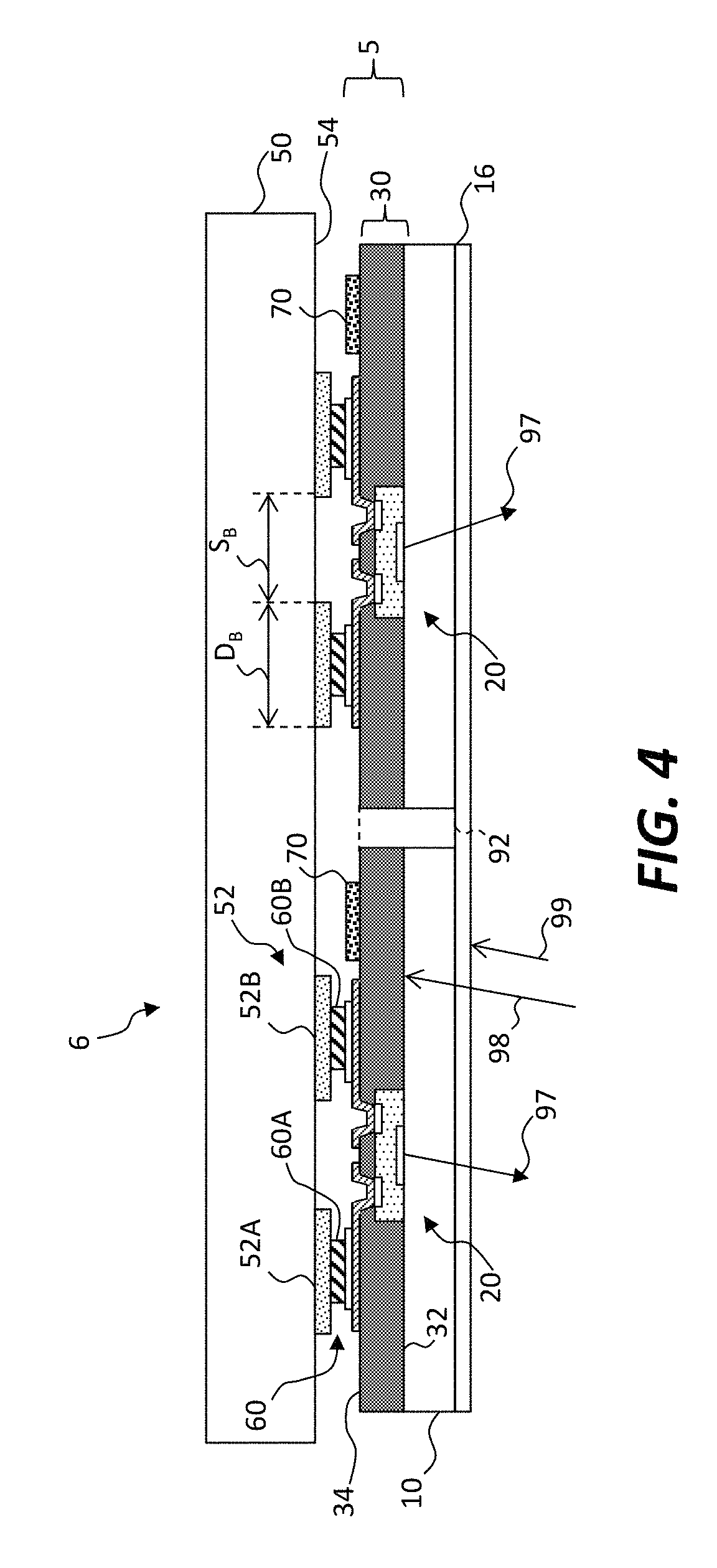
In a further embodiment of the present invention, referring to FIG. 4, a tiled display 6 includes a plurality of display tile structures 5. Each display tile structure 5 can be an individual tile 5 (e.g., even if the tile 5 does not include the tile substrate 10) in the tiled display 6 and each tile 5 includes a separate tile layer 30 with one or more light emitters 20. The tiles 5 are affixed to a backplane 50 having first and second backplane contact pads 52A, 52B (collectively 52) on a backplane surface 54 of the backplane 50. The backplane side 34 of the tile layer 30 of each tile 5 is adjacent to the backplane surface 54 having the first and second backplane contact pads 52A, 52B. A first electrical connector 60A electrically connects the first tile contact pad 12A to the first backplane contact pad 52A and a second electrical connector 60B electrically connects the second tile contact pad 12B to the second backplane contact pad 52B. When a voltage difference is supplied across the first and second backplane contact pads 52A, 52B, current flows through the first and second electrical connectors 60A, 60B (collectively electrical connectors 60) into the light emitters 20 to cause the light emitters 20 to emit light 97.
As shown in FIG. 4, in a further embodiment, the tiled display 6 includes a plurality of tiles 5 having tile layers 30 each with one or more light emitters 20 arranged in a regular array. An index-matching material 92 or a light-absorbing layer can be located between the tile layers 30. For example, the index-matching material 92 can be matched to the tile substrate 10 to reduce reflections or refractions of ambient light. Moreover, as shown in FIG. 4, the tile layer 30 and an anti-reflection layer 16 coated on the tile substrate 10 absorb ambient light 98, 99, thereby improving tiled display 6 contrast.
The backplane contact pads 52 can have a minimum backplane-contact-pad dimension D.sub.B over the backplane 50 that is greater than the tile-contact-pad dimension D.sub.CP. Alternatively or in addition, the backplane-contact-pad separation S.sub.B is greater than the tile-contact-pad separation S.sub.CP. These dimensions help to ensure that the backplane contact pads 52 are not shorted together by the tile contact pads 12, in the case of misalignment between the backplane 50 and the tiles 5.
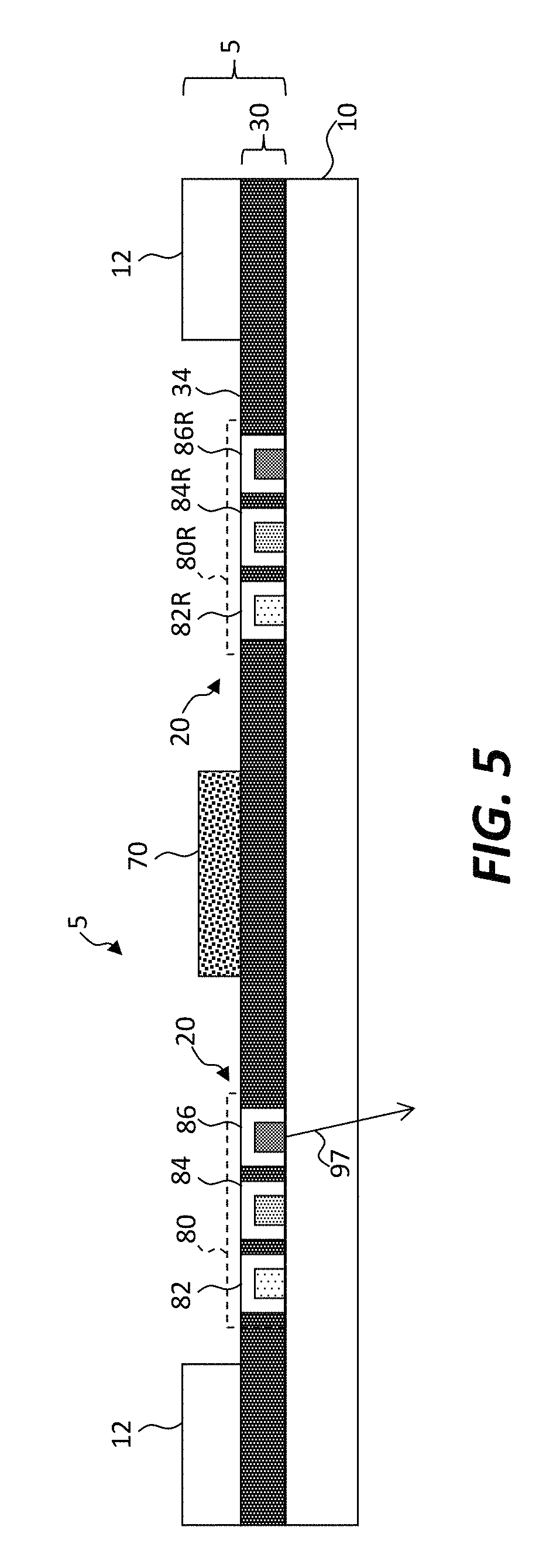
Referring to FIG. 5, in a further embodiment of the present invention, the light-emitter 20 can be a red-light emitter 82, a green-light emitter 84, or a blue-light emitter 86, or other color light emitter 20 (for example yellow or cyan). Moreover, in an embodiment, the display tile structure 5 can include a red-light emitter 82, a green-light emitter 84, and a blue-light emitter 86, and another color light emitter 20 (for example yellow or cyan). Each tile layer 30 has a corresponding plurality of light emitters 20 that each has electrodes 22 electrically connected to tile micro-wires 40, respectively. The plurality of light emitters 20 can therefore be arranged to form full-color pixels 80 in the tiled display 6.
In a further embodiment of the present invention, some of the plurality of light emitters 20 can be redundant light emitters 20 forming a redundant full-color pixel 80R, for example redundant red-light emitters 82R, redundant green-light emitters 84R, or redundant blue-light emitters 86R, arranged to emit light 97 from the emitter side 32 of the tile layer 30. The redundant red-, green-, and blue-light emitters 82R, 84R, 86R each have electrodes 22 electrically connected to a tile micro-wire 40, respectively (FIG. 1). Redundant light emitters 20 can be disposed on a common tile substrate 10 (as shown in FIG. 5) or on a separate tile substrate 10 and can be controlled with a common electrical component 70 or a separate electrical component 70.
Referring to FIG. 6, the tiled display 6 of the present invention can include a plurality of tiles 5. Each of the tiles 5 can have a plurality of tile contact pads 12. The tile contact pads 12 include perimeter tile contact pads 13 spaced around the perimeter of the tile layer 30 and can include at least one interior tile contact pad 15 located within the interior of the tile layer 30. An interior tile contact pad 15 is a tile contact pad 12 for which a perimeter tile contact pad 13 is closer to an edge of the tile layer 30 than the interior tile contact pad 15 in any direction. By arranging the tile contact pads 12 with both interior and perimeter tile contact pads 15, 13, for example in a two-dimensional arrangement as shown, the tile contact pads 12 are spatially more densely arranged than if the contact pads are located around the tile perimeter, reducing the area needed to interconnect tiles 5 to the backplane 50. In an arrangement, one or more active electrical components 70 mounted on to the backplane side 34 of the tile layer 30 (FIG. 5) is electrically connected to an interior tile contact pad 15 and the plurality of perimeter tile contact pads 13 are connected to the light emitters. This arrangement provides a useful and efficient wiring layout and the tiles and light emitters 20 can be spaced over the backplane 50 in a regular array at low cost.
As shown in FIG. 7, in another embodiment of the invention, the display tile structure 5 includes a tile heat-transfer structure 90, for example a heat-spreading layer, on or in the tile layer 30 and, for example, including metal, silicon carbide, or carbon. The tile heat-transfer structure 90 is in thermal communication with a corresponding backplane heat-transfer structure 91 on the backplane 50. The tile heat-transfer structure 90 does not have to be in physical contact with the backplane heat-transfer structure 91 so long as heat generated on the tile 5, for example by the light emitters 20, is transferred and distributed to the backplane 50, thereby reducing the temperature and temperature variability of the light emitters 20 and improving their lifetime and output uniformity. In an embodiment, the thermal communication is at least partly through the electrical connectors 60 and can be, for example, a solder bond or an anisotropic conductive film between the tile contact pads 12 of the tile 5 and the backplane contact pads 52 of the backplane 50.
In various embodiments of the present invention, the tile layer 30 includes glass, a polymer, a curable polymer, sapphire, silicon carbide, copper or diamond, or a high thermal conductivity material. The curable polymer can be light absorbing, black or impregnated with or include light-absorbing particles or pigments, such as carbon black or light-absorbing dyes or include color-conversion materials, phosphors, single-crystal fluorophors, or nanocrystals. The tile layer 30 can be a black matrix. Such materials can be coated, for example by spray, curtain, or spin coating, cured with heat or electromagnetic radiation, and patterned using photolithographic methods.
The electrodes 22, tile micro-wires 40, or tile contact pads 12 can be metal, for example aluminum, silver, gold, tantalum, tungsten, titanium, or include metals or metal alloys, conductive metal oxides, or conductive inks having conductive particles. Deposition and patterning methods, for example using evaporative coating and photolithography, or inkjet deposition and curing can be used to form the electrodes 22, micro-wires 40, and tile contact pads 12. The same or different methods may be used to form the electrodes 22, micro-wires 40, and tile contact pads 12.
The electrical connectors 60 can be metal interconnect structures, solder, solder balls, reflowed solder, anisotropic conductive film (ACF), metal pillars, pins (e.g., similar to integrated circuit pins), or connector pins (e.g., as used in the printed-circuit board industry).
The tile substrate 10 can be glass, plastic, polymer, metal or any material that provides a suitable surface (e.g., on the substrate structure side 14) for disposing, making, or forming the elements of the display tile structure 5. The tile substrate 10 can be flexible or rigid. Backplanes 50 can be printed circuit boards, for example including glass, ceramic, epoxy, resin, or polymer and can be made in a layered structure with conductive traces as are known in the printed-circuit board industry. The backplane 50 can be rigid or flexible. The tiles 5 can be connected to the backplane 50 with soldered connections, using surface mount structures and techniques, or using connectors and plugging the tiles into backplane connectors. The tiled display 6 can be flexible or rigid.
In one embodiment of the present invention, the light emitters 20 are formed on a native semiconductor wafer (e.g., GaN) and then disposed on the tile substrate 10 using micro transfer printing. For example, U.S. Pat. No. 8,722,458 entitled Optical Systems Fabricated by Printing-Based Assembly teaches transferring light-emitting, light-sensing, or light-collecting semiconductor elements from a wafer substrate to a destination substrate. Additional details useful in understanding and performing aspects of the present invention are described in U.S. patent application Ser. No. 14/743,981, filed Jun. 18, 2015 and entitled Micro-Assembled Micro LED Displays and Lighting Elements. Furthermore, the structure of the tiled display 6 of the present invention can be formed using micro-transfer techniques, for example using a multi-step transfer or assembly process. By employing such a multi-step transfer or assembly process, increased yields are achieved and thus reduced costs. A discussion of compound micro-assembly structures and methods is provided in U.S. Patent Application Ser. No. 62/055,472 filed Sep. 25, 2014, entitled Compound Micro-Assembly Strategies and Devices.
Referring to the flow diagram of FIG. 8, a method of the present invention includes providing a substrate (e.g., tile substrate 10 having a substrate structure side 14) in step 100, providing light emitters 20 such as micro-LEDs in step 105, and providing pixel controllers, such as active integrated circuit electrical components 70, in step 107. In step 110, one or more light emitters 20 are disposed on the structure side 14 of the tile substrate 10, for example by micro transfer printing, so that each light emitter 20 has a light-emitting side 24 adjacent to the structure side 14 and an opposed connection side 26 with electrodes 22 for providing electrical power to the light emitter 20 to cause the light emitter 20 to emit light 97 from the light-emitting side 24 of the light emitter 20 through the tile substrate 10.
In step 120, a tile layer 30 is formed on or over the light emitters 20 and structure side 14 of the tile substrate 10. The tile layer 30 has an emitter side 32 adjacent to the substrate structure side 14 of the tile substrate 10 and a backplane side 34 opposite the emitter side 32. The electrodes 22 are exposed in step 130, for example by pattern-wise exposing a curable light-absorbent material 36 of the tile layer 30 and developing the light-absorbent material 36 to form vias 38. Optionally, the pixel controller (e.g., an active electrical component 70) provided in step 170 is disposed on the tile layer 30 in step 140, for example by micro-transfer printing. Tile micro-wires 40 are formed in step 150 on or in the backplane side 34 of the tile layer 30 and electrically connected to the electrodes 22, for example using photolithographic processes to pattern a deposited blanket of electrically conductive metal, for example aluminum or silver, or materials including metal. Tile contact pads 12, are formed in step 160 to electrically connect to the tile micro-wires 40. The tile micro-wires 40 and the tile contact pads 12 can be formed exclusively on the backplane side 34 or in, or partially in, the backplane side 34 of the tile layer 30 so that no tile micro-wire 40 or tile contact pad 12 is in contact with the substrate structure side 14 of the tile substrate 10. In an embodiment, the tile micro-wires 40 and tile contact pads 12 are formed in a common step with common materials so that steps 150 and 160 are the same step. Furthermore, if electrical components 70 are present, they can be electrically connected to the tile micro-wires 40, tile contact pads 12, or electrodes 22 in the same step. In an embodiment, the tile substrate 10 is a large substrate and multiple display tile structures 5 are formed on the display tile substrate 10 at the same time with the same materials and with the same steps. The multiple display tile structures 5 can be singulated into portions that each include one or more light emitters 20, tile micro-wires 40, and tile contact pads 12 to provide individual display tile structures 5 or groups of display tile structures 5 on a common substrate in optional step 170.
Referring to the flow diagram of FIG. 9, a backplane 50 is provided in step 109, for example a printed circuit board, and backplane contact pads 52 formed in step 180 on a backplane surface 54 of the backplane 50, for example using conventional printed circuit board materials and manufacturing methods such as plated or etched copper. In step 190, solder is provided on the tile contact pads 12 or the backplane contact pads 52 (providing electrical connectors 60), the tiles 5 are assembled to the backplane 50 in step 200, thereby disposing the backplane side 34 of the tile layer 30 adjacent to the backplane surface 54 so that the backplane contact pads 52 are located in spatial correspondence with the tile contact pads 12, and the assembled structure is processed, for example with heat in step 210, to adhere and electrically connect the tile contact pads 12 to the backplane contact pads 52 with electrical connectors 60 and form the tiled display 6. This processing step can also align the tiles 5, for example using surface tension effects from the tile contact pads 12 and the backplane contact pads 52 with melted solder. Alternatively, tiles 5 can be plugged into sockets or connectors to electrically connect and align the backplane contact pads 52 to the tile contact pads 12. In an optional step, and as shown in FIG. 7, the tile substrate 10 is removed in step 220 from the emitter side 32 of the tile layer 30 and the light-emitting side 24 of the light emitters 20. To enable removal, a release layer or light adhesive can be included in the tile substrate 10 on which the light emitters 20 are disposed and the light-absorbing material 36 coated. A protective layer 18, structure, light-controlling layer, diffuser, or light-extraction layer can be formed over the exposed emitter side 32 of the tile layer 30 and the light-emitting side 24 of the light emitters 20. Alternatively or in addition, an index-matching material 92 or light-absorbing material 36 can be disposed in any gaps between the tiles 5, for example by coating a light-controlling material in step 230. Anti-reflection layers 16 (FIG. 4) can also be used. By removing the tile substrate 10, a thinner or more flexible tiled display 6 is formed.
In a further embodiment, a tile heat-transfer structure 90 is formed on or in the tile layer 30. A backplane heat-transfer structure 91 is formed on the backplane 50 and thermally connected to the tile heat-transfer structure 90.
The present invention provides a simple, inexpensive, and robust way to construct a display tile structure 5 and tiled display 6. The invention reduces process steps and provides a simple and robust light output structure well suited to micro transfer printing of micro-LED light emitters useful in making large, high-resolution displays. The structure described is not suitable to organic light emitting diode (OLED) or liquid crystal (LC) displays since those display structures employ vertical electrode structures that require transparent conductors (for example transparent conductive oxides) electrically connected through vias constructed through substrates, around the edges of substrates, or are connected on both sides of a substrate, all of which compromise the utility or integrity of the device and are problematic for environmentally sensitive materials, and add cost. In particular, OLED and LC displays require electrical connections to the light-emitting side 24 of the display device. Furthermore, OLED and LC materials require environmental protection and sealed structure not needed for the present invention. The present invention also enables bottom emission (if the tile substrate 10 is present), which is not possible in LC displays because of the backlight. In another embodiment (e.g., as illustrated in FIG. 7) no conventional substrate is present at all in the assembled display, thus improving light output and reducing thickness. Furthermore, the present invention provides structures that locate circuitry connections or integrated circuits that are present in or behind the display area, further improving component density and display resolution and improving utility and functionality.
As is understood by those skilled in the art, the terms "over" and "under" are relative terms and can be interchanged in reference to different orientations of the layers, elements, and substrates included in the present invention. For example, a first layer on a second layer, in some implementations means a first layer directly on and in contact with a second layer. In other implementations a first layer on a second layer includes a first layer and a second layer with another layer therebetween.
Having described certain implementations of embodiments, it will now become apparent to one of skill in the art that other implementations incorporating the concepts of the disclosure may be used. Therefore, the invention should not be limited to the described embodiment, but rather should be limited only by the spirit and scope of the following claims.
Throughout the description, where apparatus and systems are described as having, including, or comprising specific components, or where processes and methods are described as having, including, or comprising specific steps, it is contemplated that, additionally, there are apparatus, and systems of the disclosed technology that consist essentially of, or consist of, the recited components, and that there are processes and methods according to the disclosed technology that consist essentially of, or consist of, the recited processing steps.
It should be understood that the order of steps or order for performing certain action is immaterial so long as the disclosed technology remains operable. Moreover, two or more steps or actions in some circumstances can be conducted simultaneously. The invention has been described in detail with particular reference to certain embodiments thereof, but it will be understood that variations and modifications can be effected within the spirit and scope of the invention.
PARTS LIST
D.sub.B backplane-contact-pad dimension D.sub.CP tile-contact-pad dimension D.sub.E electrode width S.sub.B backplane-contact-pad separation S.sub.CP tile-contact-pad separation S.sub.E electrode separation 5 display tile structure/tile 6 tiled display 10 tile substrate 12 tile contact pad 12A first tile contact pad 12B second tile contact pad 13 perimeter tile contact pad 14 substrate structure side 15 interior tile contact pad 16 anti-reflection layer 18 protective layer 20 light emitter 21 semiconductor layers 21C conductive semiconductor layer 21P p-doped semiconductor layer 21N n-doped semiconductor layer 22 light-emitter contact pad/electrode 22A first light-emitter contact pad/first electrode 22B second light-emitter contact pad/second electrode 23 dielectric layer 24 light-emitting side 26 connection side 28 light-emitting area 30 tile layer 32 emitter side 34 backplane side 36 light-absorbing material 37 dielectric sub-layer/interlayer dielectric 38 via 40 tile micro-wire 40A first tile micro-wire 40B second tile micro-wire 50 backplane 52 backplane contact pads 52A first backplane contact pad 52B second backplane contact pad 60 backplane surface 60 electrical connector 60A first electrical connector 60B second electrical connector 70 electrical component 80 full-color pixel 80R redundant pixel 82 red-light emitter 82R redundant red-light emitter 84 green-light emitter 84R redundant green-light emitter 86 blue-light emitter 86R redundant blue-light emitter 90 tile heat-transfer structure 91 backplane heat-transfer structure 92 index-matching material 97 emitted light 98 ambient light 99 ambient light 100 provide substrate step 105 provide light emitters step 107 provide pixel controller step 109 provide backplane step 110 dispose light emitters step 120 form tile layer over light emitters step 130 expose electrodes step 140 dispose pixel controller step 150 form micro-wires step 160 form tile contact pads step 170 singulate tiles step 180 form backplane contact pads step 190 provide solder on contact pads step 200 assemble tile to backplane step 210 solder backplane contact pads to tile contact pads step 220 remove substrate step 230 coat light-controlling material step
* * * * *
D00000
D00001
D00002
D00003
D00004
D00005
D00006
D00007
D00008
XML
uspto.report is an independent third-party trademark research tool that is not affiliated, endorsed, or sponsored by the United States Patent and Trademark Office (USPTO) or any other governmental organization. The information provided by uspto.report is based on publicly available data at the time of writing and is intended for informational purposes only.
While we strive to provide accurate and up-to-date information, we do not guarantee the accuracy, completeness, reliability, or suitability of the information displayed on this site. The use of this site is at your own risk. Any reliance you place on such information is therefore strictly at your own risk.
All official trademark data, including owner information, should be verified by visiting the official USPTO website at www.uspto.gov. This site is not intended to replace professional legal advice and should not be used as a substitute for consulting with a legal professional who is knowledgeable about trademark law.