Semiconductor apparatus and method of manufacturing the same
Zhang , et al. J
U.S. patent number 10,177,127 [Application Number 15/007,959] was granted by the patent office on 2019-01-08 for semiconductor apparatus and method of manufacturing the same. This patent grant is currently assigned to Hong Kong Beida Jade Bird Display Limited. The grantee listed for this patent is Hong Kong Beida Jade Bird Display Limited. Invention is credited to Wing Cheung Chong, Qiming Li, Fang Ou, Huiwen Xu, Lei Zhang.


View All Diagrams
| United States Patent | 10,177,127 |
| Zhang , et al. | January 8, 2019 |
Semiconductor apparatus and method of manufacturing the same
Abstract
A semiconductor apparatus includes a driver circuit wafer including a plurality of driver circuits arranged in an array, a bonding metal layer formed over the driver circuit wafer, and a horizontally continuous functional device epi-structure layer formed over the bonding metal layer and covering the driver circuits.
| Inventors: | Zhang; Lei (Albuquerque, NM), Li; Qiming (Albuquerque, NM), Xu; Huiwen (Shanghai, CN), Ou; Fang (Monterey Park, CA), Chong; Wing Cheung (Hong Kong, CN) | ||||||||||
|---|---|---|---|---|---|---|---|---|---|---|---|
| Applicant: |
|
||||||||||
| Assignee: | Hong Kong Beida Jade Bird Display
Limited (Hong Kong, CN) |
||||||||||
| Family ID: | 58186923 | ||||||||||
| Appl. No.: | 15/007,959 | ||||||||||
| Filed: | January 27, 2016 |
Prior Publication Data
| Document Identifier | Publication Date | |
|---|---|---|
| US 20170069609 A1 | Mar 9, 2017 | |
Related U.S. Patent Documents
| Application Number | Filing Date | Patent Number | Issue Date | ||
|---|---|---|---|---|---|
| 62214395 | Sep 4, 2015 | ||||
| 62258072 | Nov 20, 2015 | ||||
| 62259810 | Nov 25, 2015 | ||||
| Current U.S. Class: | 1/1 |
| Current CPC Class: | H01S 5/183 (20130101); H01L 33/60 (20130101); H01L 25/0753 (20130101); H01L 33/62 (20130101); H01L 25/167 (20130101); H01S 5/0216 (20130101); H01L 33/58 (20130101); H01S 5/042 (20130101); H01S 5/0261 (20130101); H01L 2224/32145 (20130101); H01L 2224/92244 (20130101); H01S 5/0217 (20130101); H01L 33/0093 (20200501); H01S 5/423 (20130101); H01L 2224/73267 (20130101); H01L 2224/82 (20130101); H01L 2933/0066 (20130101) |
| Current International Class: | H01L 25/16 (20060101); H01L 33/58 (20100101); H01L 33/60 (20100101); H01L 33/62 (20100101); H01S 5/183 (20060101); H01S 5/02 (20060101); H01L 25/075 (20060101); H01S 5/042 (20060101); H01S 5/026 (20060101); H01S 5/42 (20060101); H01L 33/00 (20100101) |
References Cited [Referenced By]
U.S. Patent Documents
| 3950738 | April 1976 | Hayashi |
| 5264699 | November 1993 | Barton |
| 5621225 | April 1997 | Shieh |
| 5624174 | April 1997 | Loucks |
| 5653522 | August 1997 | Loucks |
| 6005262 | December 1999 | Cunningham |
| 6262540 | July 2001 | Seko |
| 7829902 | November 2010 | El-Ghoroury |
| 8535961 | September 2013 | Kuo |
| 8557616 | October 2013 | Lau et al. |
| 8567960 | October 2013 | El-Ghoroury et al. |
| 8642363 | February 2014 | Lau et al. |
| 8851682 | October 2014 | Tanigawa et al. |
| 8931906 | January 2015 | Huang et al. |
| 9041025 | May 2015 | Lau et al. |
| 2002/0135553 | September 2002 | Nagai et al. |
| 2002/0153529 | October 2002 | Shie |
| 2002/0196431 | December 2002 | DeFelice |
| 2004/0208596 | October 2004 | Bringans |
| 2005/0067944 | March 2005 | Masuda et al. |
| 2006/0023167 | February 2006 | Chiang et al. |
| 2006/0274189 | December 2006 | Mouli |
| 2007/0099395 | May 2007 | Sridhar |
| 2007/0211492 | September 2007 | Lin |
| 2008/0308820 | December 2008 | Louwsma |
| 2009/0085045 | April 2009 | Marion |
| 2010/0020502 | January 2010 | Tain et al. |
| 2010/0283069 | November 2010 | Rogers et al. |
| 2010/0295070 | November 2010 | Su et al. |
| 2010/0327386 | December 2010 | Nagai |
| 2011/0096045 | April 2011 | Ito et al. |
| 2011/0169157 | July 2011 | Fan |
| 2011/0233586 | September 2011 | Kojima et al. |
| 2011/0300644 | December 2011 | Akimoto et al. |
| 2012/0043563 | February 2012 | Ibbetson et al. |
| 2012/0050694 | March 2012 | Huang |
| 2012/0220059 | August 2012 | Ito |
| 2012/0223875 | September 2012 | Lau |
| 2012/0288995 | November 2012 | El-Ghoroury |
| 2013/0002730 | January 2013 | Tanigawa et al. |
| 2013/0126081 | May 2013 | Hu |
| 2013/0126098 | May 2013 | Bibl et al. |
| 2013/0126827 | May 2013 | Bibl et al. |
| 2013/0126914 | May 2013 | Pan |
| 2013/0126921 | May 2013 | Mohammed et al. |
| 2013/0128585 | May 2013 | Bibl et al. |
| 2013/0130440 | May 2013 | Hu et al. |
| 2013/0187174 | July 2013 | Tischler |
| 2013/0207964 | August 2013 | Fleck |
| 2013/0210194 | August 2013 | Bibl et al. |
| 2013/0217161 | August 2013 | Hsu |
| 2013/0240962 | September 2013 | Wang |
| 2014/0008667 | January 2014 | Lau et al. |
| 2014/0008813 | January 2014 | Golda et al. |
| 2014/0048909 | February 2014 | Golda et al. |
| 2014/0061687 | March 2014 | Hu et al. |
| 2014/0061705 | March 2014 | Tischler |
| 2014/0084482 | March 2014 | Hu et al. |
| 2014/0091420 | April 2014 | Payne |
| 2014/0111408 | April 2014 | Lau et al. |
| 2014/0158415 | June 2014 | Golda et al. |
| 2014/0159043 | June 2014 | Sakariya et al. |
| 2014/0159064 | June 2014 | Sakariya et al. |
| 2014/0159065 | June 2014 | Hu et al. |
| 2014/0159066 | June 2014 | Hu et al. |
| 2014/0159067 | June 2014 | Sakariya et al. |
| 2014/0159324 | June 2014 | Golda et al. |
| 2014/0168037 | June 2014 | Sakariya et al. |
| 2014/0168988 | June 2014 | Petersen et al. |
| 2014/0169924 | June 2014 | Golda et al. |
| 2014/0169927 | June 2014 | Golda et al. |
| 2014/0196851 | July 2014 | Golda et al. |
| 2014/0209248 | July 2014 | Golda et al. |
| 2014/0218912 | August 2014 | Guehne et al. |
| 2014/0241843 | August 2014 | Golda et al. |
| 2014/0241844 | August 2014 | Golda et al. |
| 2014/0267683 | September 2014 | Bibl et al. |
| 2014/0319560 | October 2014 | Tischler |
| 2014/0340900 | November 2014 | Bathurst et al. |
| 2014/0367633 | December 2014 | Bibl et al. |
| 2014/0367705 | December 2014 | Bibl et al. |
| 2014/0367711 | December 2014 | Bibl et al. |
| 2015/0003056 | January 2015 | Choi et al. |
| 2015/0008389 | January 2015 | Hu et al. |
| 2015/0021466 | January 2015 | Bibl et al. |
| 2015/0028362 | January 2015 | Chan et al. |
| 2015/0071320 | March 2015 | Gronenborn |
| 2015/0076528 | March 2015 | Chan et al. |
| 2015/0093842 | April 2015 | Higginson et al. |
| 2015/0137153 | May 2015 | Bibl et al. |
| 2015/0169011 | June 2015 | Bibl et al. |
| 2015/0179703 | June 2015 | Sakariya et al. |
| 2015/0179876 | June 2015 | Hu et al. |
| 2015/0179877 | June 2015 | Hu et al. |
| 2015/0187740 | July 2015 | McGroddy et al. |
| 2015/0187991 | July 2015 | McGroddy et al. |
| 2015/0214420 | July 2015 | Hu et al. |
| 2015/0216042 | July 2015 | Golda et al. |
| 2015/0228525 | August 2015 | Golda et al. |
| 2015/0235121 | August 2015 | Pavate et al. |
| 2016/0276329 | September 2016 | Bono |
| 1619846 | May 2005 | CN | |||
| 101241882 | Aug 2008 | CN | |||
| 101634800 | Jan 2010 | CN | |||
| 201464787 | May 2010 | CN | |||
| 101064330 | Oct 2017 | CN | |||
| 2012-19201 | Jan 2012 | JP | |||
Other References
|
International Search Report and Written Opinion issued by the State Intellectual Property Office (SIPO) of the People's Republic of China for International Application No. PCT/IB2016/001259 dated Jan. 22, 2017. cited by applicant . International Search Report and Written Opinion issued by the State Intellectual Property Office (SIPO) of the People's Republic of China for International Application No. PCT/IB2016/001342 dated Feb. 17, 2017. cited by applicant . International Search Report and Written Opinion issued by the State Intellectual Property Office (SIPO) of the People's Republic of China for International Application No. PCT/IB2016/001260 dated Dec. 28, 2016. cited by applicant . Office Action for U.S. Appl. No. 15/239,467 dated Apr. 4, 2017. cited by applicant . Office Action for U.S. Appl. No. 15/246,447 dated Aug. 25, 2017. cited by applicant. |
Primary Examiner: King; Joshua
Attorney, Agent or Firm: Finnegan, Henderson, Farabow, Garrett & Dunner, LLP.
Parent Case Text
CROSS-REFERENCE TO RELATED APPLICATIONS
This application is based upon and claims the benefit of priority from Provisional Application No. 62/214,395, 62/258,072, and 62/259,810, filed on Sep. 4, 2015, Nov. 20, 2015, and Nov. 25, 2015, respectively, the entire contents of all of which are incorporated herein by reference.
Claims
What is claimed is:
1. A semiconductor apparatus, comprising: a driver circuit wafer including a plurality of driver circuits arranged in an array; a bonding metal layer formed over the driver circuit wafer; a horizontally continuous unpatterned functional device epi-structure layer formed over the bonding metal layer and covering the driver circuits; and a dielectric isolation layer arranged between the driver circuit wafer and the functional device epi-structure layer, the dielectric isolation layer including first protrusion structures and second protrusion structures surrounding each of the first protrusion structures, wherein the functional device epi-structure layer includes a light-emitting device epi-structure layer, the driver circuits are configured to provide driving currents to a plurality of light-emitting devices, the bonding metal layer includes a plurality of bonding metal pads arranged in an array and isolated from each other, each of the driver circuits corresponding to one of the bonding metal pads, each first protrusion structure is formed between one of the bonding metal pads and one of the driver circuits, and has a through hole formed from an upper surface of the first protrusion structure to a lower surface of the first protrusion structure, at least a portion of the bonding metal pad being arranged in the through hole, and each of the first protrusion structures and the second protrusion structures surrounding the first protrusion structure define a continuous recess surrounding the first protrusion structure.
2. The semiconductor apparatus of claim 1, wherein the light-emitting device epi-structure layer includes a light-emitting diode (LED) epi-structure layer.
3. The semiconductor apparatus of claim 1, wherein the light-emitting device epi-structure layer includes a vertical cavity surface emitting laser (VCSEL) epi-structure layer.
4. The semiconductor apparatus of claim 1, wherein the light-emitting device epi-structure layer is a first light-emitting device epi-structure layer associated with a first wavelength, the semiconductor apparatus further comprising: a second light-emitting device epi-structure layer formed over the first light-emitting device epi-structure layer and associated with a second wavelength different from the first wavelength.
5. The semiconductor apparatus of claim 4, wherein the bonding metal layer is a first bonding metal layer, the semiconductor apparatus further comprising: a second bonding metal layer formed between the first and second light-emitting device epi-structure layers.
6. The semiconductor apparatus of claim 4, further comprising: one or more additional light-emitting device epi-structure layers formed over the second light-emitting device epi-structure layer, each of the one or more light-emitting device epi-structure layers being associated with a wavelength different from the first and second wavelengths.
7. The semiconductor apparatus of claim 6, further comprising: one or more additional bonding metal layers, each of the one or more additional bonding metal layers being formed below one of the one or more additional light-emitting device epi-structure layers.
8. The semiconductor apparatus of claim 1, wherein the bonding metal layer includes a horizontally continuous bonding metal layer covering the driver circuits.
9. A semiconductor apparatus, comprising: a single crystalline driver circuit wafer including a plurality of driver circuits arranged in an array; a bonding metal layer formed over the driver circuit wafer, the bonding metal layer including a plurality of bonding metal pads arranged in an array and isolated from each other, each of the driver circuits corresponding to and electrically coupled to one of the bonding metal pads; a functional device epi-layer formed over the bonding metal layer, the functional device epi-layer including a plurality of light-emitting device dies arranged in an array, each of the plurality of light-emitting device dies corresponding to one of the bonding metal pads; and a dielectric isolation layer arranged between the single crystalline driver circuit wafer and the functional device epi-layer, the dielectric isolation layer including first protrusion structures and second protrusion structures surrounding each of the first protrusion structures, wherein adjacent light-emitting device dies are separated from each other with no epi-layer connecting each other at a first surface of the light-emitting device dies opposite to a second surface of the light-emitting device dies where the bonding metal layer is formed, wherein the driver circuits are configured to provide driving currents to the plurality of light-emitting device dies, wherein each first protrusion structure is formed between one of the bonding metal pads and one of the driver circuits, and has a through hole formed from an upper surface of the first protrusion structure to a lower surface of the first protrusion structure, at least a portion of the bonding metal pad being arranged in the through hole, and each of the first protrusion structures and the second protrusion structures surrounding the first protrusion structure define a continuous recess surrounding the first protrusion structure.
10. The semiconductor apparatus of claim 9, wherein the light-emitting device dies are configured to be optically isolated from each other.
11. The semiconductor apparatus of claim 10, further comprising: an isolation layer formed between the light-emitting device dies.
12. The semiconductor apparatus of claim 11, wherein the isolation layer includes a material that is absorptive of or reflective to light having a wavelength associated with the light-emitting device dies.
13. The semiconductor apparatus of claim 11, further comprising: a cross-connected metal layer formed over the isolation layer and being electrically coupled to ground pads of the driver circuits and the top surfaces of the light-emitting device dies.
14. The semiconductor apparatus of claim 9, wherein: the light-emitting device dies include: a first light-emitting device die including a first active layer associated with a first wavelength; a second light-emitting device die including a second active layer formed over a first dummy layer and associated with a second wavelength; and a third light-emitting device die including a third active layer formed over a second dummy layer and associated with a third wavelength, the second dummy layer being formed over a third dummy layer, the first active layer, the first dummy layer, and the third dummy layer are made from a first material, and the second active layer and the second dummy layer are made from a second material.
15. The semiconductor apparatus of claim 9, wherein the light-emitting device dies include a plurality of light-emitting diode (LED) dies.
16. The semiconductor apparatus of claim 9, wherein the light-emitting device dies include a plurality of vertical cavity surface emitting laser (VCSEL) dies.
17. The semiconductor apparatus of claim 9, wherein the driver circuits include a plurality of high electron mobility transistor (HEMT) dies.
18. The semiconductor apparatus of claim 9, further comprising: an electrode layer formed between the bonding metal layer and the functional device epi-layer, the electrode layer being formed of a conducting material and including a plurality of electrodes arranged in an array, each of the electrodes corresponding to one of the bonding metal pads.
19. The semiconductor apparatus of claim 18, wherein the electrode layer includes: a reflecting layer formed over the bonding metal layer; and a transparent conducting layer formed over the reflecting layer.
20. A semiconductor apparatus, comprising: a driver circuit wafer including a plurality of driver circuits arranged in an array; a bonding metal layer formed over the driver circuit wafer; a horizontally continuous functional device epi-structure layer formed over the bonding metal layer and covering the driver circuits, wherein every layer of the horizontally continuous functional device epi-structure layer is substantially continuous or unpatterned; and a dielectric isolation layer arranged between the driver circuit wafer and the functional device epi-structure layer, the dielectric isolation layer including first protrusion structures and second protrusion structures surrounding each of the first protrusion structures, wherein the functional device epi-structure layer includes a light-emitting device epi-structure layer, the driver circuits are configured to provide driving currents to a plurality of light-emitting devices, the bonding metal layer includes a plurality of bonding metal pads arranged in an array and isolated from each other, each of the driver circuits corresponding to one of the bonding metal pads, each first protrusion structure is formed between one of the bonding metal pads and one of the driver circuits, and has a through hole formed from an upper surface of the first protrusion structure to a lower surface of the first protrusion structure, at least a portion of the bonding metal pad being arranged in the through hole, and each of the first protrusion structures and the second protrusion structures surrounding the first protrusion structure define a continuous recess surrounding the first protrusion structure.
Description
TECHNOLOGY FIELD
The disclosure relates to a semiconductor apparatus and, more particularly, to a semiconductor apparatus including a driver circuit wafer and a functional device epi-layer formed thereover, and a method of manufacturing the semiconductor apparatus.
BACKGROUND
In many conventional semiconductor systems, functional devices and their control circuits are often separately formed on different wafers or on different regions of a same wafer. They are then connected to each other via wirings, etc. Sometime the wirings can be long and convoluted, resulting in high power consumption and signal cross-talk. Moreover, conventional semiconductor systems can be bulky and difficult to miniaturize.
SUMMARY
In accordance with the disclosure, there is provided a semiconductor apparatus including a driver circuit wafer, a bonding metal layer formed over the driver circuit wafer, and a horizontally continuous functional device epi-structure layer formed over the bonding metal layer. The driver circuit wafer includes a plurality of driver circuits arranged in an array. The functional device epi-structure layer covers the driver circuits.
Also in accordance with the disclosure, there is provided a semiconductor apparatus including a single crystalline driver circuit wafer, a bonding metal layer formed over the driver circuit wafer, and a functional device epi-layer formed over the bonding metal layer. The driver circuit wafer includes a plurality of driver circuits arranged in an array. The bonding metal layer includes a plurality of bonding metal pads arranged in an array and isolated from each other. Each of the driver circuits corresponds to and is electrically coupled to one of the bonding metal pads. The functional device epi-layer includes a plurality of functional device dies arranged in an array. Each of the functional device dies corresponds to one of the bonding metal pads.
Also in accordance with the disclosure, there is provided a method for fabricating a semiconductor apparatus. The method includes forming a first pre-bonding metal layer over a driver circuit wafer. The driver circuit wafer includes a plurality of driver circuits arranged in an array. The method further includes forming a second pre-bonding metal layer over a functional device wafer. The functional device wafer includes a functional device epi-structure layer epitaxially grown on a growth substrate. The method also includes bonding the functional device wafer onto the driver circuit wafer through the first and second pre-bonding metal layers and removing the growth substrate to expose the functional device epi-structure layer.
Features and advantages consistent with the disclosure will be set forth in part in the description which follows, and in part will be obvious from the description, or may be learned by practice of the disclosure. Such features and advantages will be realized and attained by means of the elements and combinations particularly pointed out in the appended claims.
It is to be understood that both the foregoing general description and the following detailed description are exemplary and explanatory only and are not restrictive of the invention, as claimed.
The accompanying drawings, which are incorporated in and constitute a part of this specification, illustrate several embodiments of the invention and together with the description, serve to explain the principles of the invention.
BRIEF DESCRIPTION OF THE DRAWINGS
FIG. 1 is a cross-sectional view schematically showing a vertically-integrated semiconductor apparatus according to an exemplary embodiment.
FIGS. 2A-2E schematically show a process for manufacturing the semiconductor apparatus of FIG. 1 according to an exemplary embodiment.
FIGS. 3A-3D schematically show a process for manufacturing the semiconductor apparatus of FIG. 1 according to another exemplary embodiment.
FIGS. 4A and 4B schematically show a process for manufacturing the semiconductor apparatus of FIG. 1 according to another exemplary embodiment.
FIGS. 5A-5B schematically show a process for manufacturing the semiconductor apparatus of FIG. 1 according to another exemplary embodiment.
FIGS. 6A and 6B schematically show a semiconductor apparatus according to another exemplary embodiment.
FIGS. 7A and 7B schematically show a semiconductor apparatus according to another exemplary embodiment.
FIGS. 8A and 8B schematically show a semiconductor apparatus according to another exemplary embodiment.
FIG. 9 schematically shows a semiconductor apparatus according to another exemplary embodiment.
FIG. 10 schematically shows an opto-electronic apparatus according to an exemplary embodiment.
FIG. 11 schematically shows an opto-electronic apparatus according to another exemplary embodiment.
FIGS. 12A-12K schematically show a process for manufacturing the opto-electronic apparatus of FIG. 11 according to an exemplary embodiment.
FIG. 13A schematically shows a light-emitting diode (LED) panel according to an exemplary embodiment.
FIG. 13B schematically shows an LED panel according to another exemplary embodiment.
DESCRIPTION OF THE EMBODIMENTS
Embodiments consistent with the disclosure include a semiconductor apparatus including a driver circuit wafer and a functional device epi-layer formed thereover, and a method of manufacturing the semiconductor apparatus.
Hereinafter, embodiments consistent with the disclosure will be described with reference to the drawings. Wherever possible, the same reference numbers will be used throughout the drawings to refer to the same or like parts.
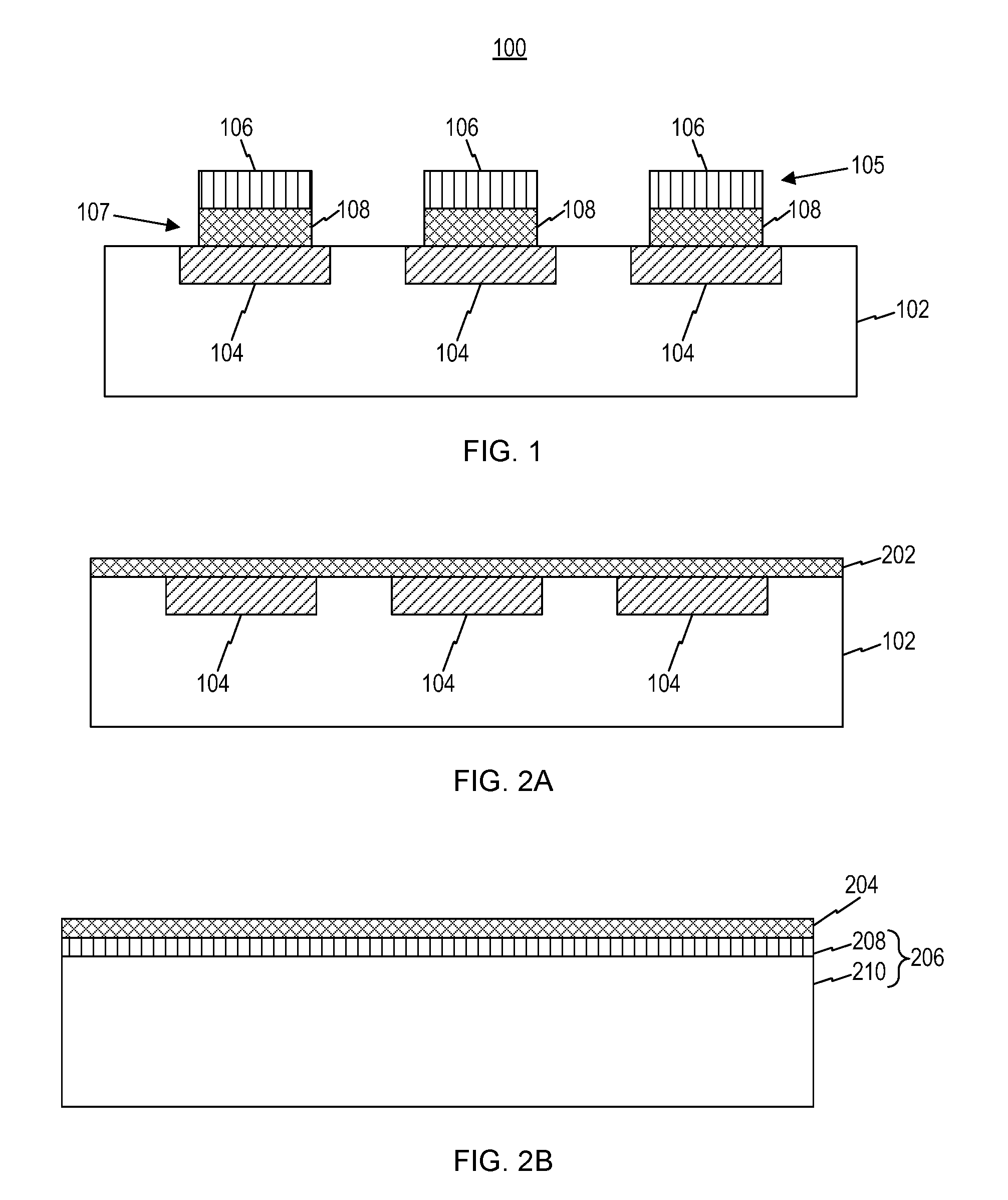
FIG. 1 is a cross-sectional view schematically showing an exemplary vertically-integrated semiconductor apparatus 100 consistent with embodiments of the present disclosure. The semiconductor apparatus 100 includes a driver circuit wafer 102 having a plurality of driver circuits 104 formed therein as an array. As used herein, the term "wafer" refers to a thin portion of material that may or may not have device structures or other fine structure formed therein. The semiconductor apparatus 100 further includes a functional device epi-layer 105 formed over the driver circuit wafer 102. The functional device epi-layer 105 includes a plurality of functional device dies 106 arranged in an array. As used herein, the term "die" refers to a small block of semiconductor material or a small area of a portion of semiconductor material that includes one or more individual functional devices. The semiconductor apparatus 100 also includes a bonding metal layer 107 formed between the driver circuit wafer 102 and the functional device epi-layer 105. The bonding metal layer 107 includes a plurality of bonding metal pads 108 arranged in an array and isolated, both spatially and electrically, from each other.
Consistent with the present disclosure, each of the driver circuits 104 corresponds to and is horizontally aligned with one of the bonding metal pads 108. In addition, each of the functional device dies 106 corresponds to and is horizontally aligned with one of the driver circuits 104 and one of the bonding metal pads 108. That is, a driver circuit 104 and a corresponding functional device 106 are bonded together through only one corresponding bonding metal pad 108. In other words, the driver circuits 104, the bonding metal pads 108, and the functional devices 106 have a one-to-one relationship.
Consistent with the present disclosure, each of the bonding metal pads 108 includes one or more electrically conductive materials, such as one or more metals or alloys, and also serves as an electrical contact between the corresponding driver circuit 104 and functional device die 106 for transmitting electrical signals therebetween. For example, the bonding material for the bonding metal pads 108 can be tin (Sn), gold (Au), nickel (Ni), palladium (Pd), or copper (Cu), or an alloy of any two or more of these metals, such as Au--Sn metal alloy. Alternatively, each of the bonding metal pads 108 can include a composite layer having multiple sublayers each including one or more suitable bonding materials or alloys thereof. Moreover, each of the bonding metal pads 108 can also include, on either one or each of the side facing the driver circuit wafer 102 and the side facing the functional device epi-layer 105, an adhesion layer and/or a bonding diffusion barrier layer. The adhesion layer facilitates the adhesion between the bonding metal pad 108 and the driver circuit wafer 102 or the corresponding functional device die 106, and the bonding diffusion barrier layer helps to prevent or reduce diffusion of the bonding material(s).
In the present disclosure, the functional device dies 106 refer to semiconductor dies that can perform certain functions. The functional device dies 106 may be the same as or different from each other. According to the present disclosure, the functional device dies 106 are configured such that no part of a growth substrate, which is used for growing epitaxial layers that are used to form the functional device dies 106, remains in the functional device dies 106.
In some embodiments, the functional device dies 106 may be opto-electronic device dies, such as light-emitting device dies or light-absorbing device dies. The light-emitting device dies may be light-emitting diode (LED) dies. The light-emitting device dies may also be laser diode (LD) dies, such as edge emitting lasers (e.g., Fabry-Perot (FP) lasers, distributed feedback (DFB) lasers, or distributed Bragg reflector (DBR) lasers) or vertical cavity surface emitting lasers (VCSELs). Examples of the light-absorbing device dies include semiconductor photodetector dies and solar cells. If the functional device dies 106 are opto-electronic device dies, each of the functional device dies 106 includes an active region associated with a certain wavelength or a certain wavelength range, i.e., the active region is configured to emit or absorb light of a certain wavelength or a certain wavelength range. As noted above, the functional device dies 106 can be the same as or different from each other. Correspondingly, the active regions of different functional device dies 106 can be associated with the same or different wavelengths or wavelength ranges.
In some embodiments, if the functional device dies 106 include LED dies, each of the functional device dies 106 can include a roughened uppermost epitaxial layer. The upper surface of the uppermost epitaxial layer is roughened to improve light extraction from the LED die.
The functional device dies 106 are not limited to opto-electronic devices, but can be other types of electrical devices. For example, the functional device dies 106 can be micro-electro-mechanical system (MEMS) dies, such as MEMS sensors. The functional device dies 106 can also be power electronic device dies, such as insulated-gate bipolar transistor (IGBT) dies, Schottky barrier diode (SBD) dies, or junction barrier Schottky (JBS) rectifier dies.
Depending on the type of the functional device dies 106, the functional device epi-layer 105 may be made of different types of materials. For example, the functional device epi-layer 105 may include elemental semiconductors (e.g., silicon (Si) or germanium (Ge)). The functional device epi-layer 105 may also include compound semiconductors, such as II-VI compound semiconductors (e.g., zinc oxide (ZnO), zinc telluride (ZnTe), and zinc sulphide (ZnS)), III-V compound semiconductors (e.g., indium-phosphide (InP) based semiconductors such as InP, indium-gallium arsenide (InGaAs), and indium-gallium arsenide phosphide (InGaAsP), gallium-arsenide (GaAs) based semiconductors such as GaAs, aluminum-gallium arsenide (AlGaAs), and gallium arsenide antimonide (GaAsSb), or gallium-nitride (GaN) based semiconductors such as GaN, indium-gallium nitride (InGaN), and aluminum-gallium nitride (AlGaN)), or IV-IV compound semiconductors (e.g., silicon carbide (SiC) or Si--Ge alloy).
In the present disclosure, the driver circuit wafer 102 is also referred to as a "driver circuit substrate" or a "carrier wafer." The driver circuit wafer 102 may include a semiconductor substrate, such as an amorphous semiconductor substrate, a polycrystalline semiconductor substrate, or a single crystalline semiconductor substrate. For example, the driver circuit wafer 102 can include a single crystalline silicon (Si) substrate or a single crystalline III-V compound semiconductor substrate. In some embodiments, the driver circuit wafer 102 may include one or more dielectric layers (not shown), such as silicon dioxide (SiO.sub.2) layers, formed over the semiconductor substrate. Wirings and/or contacts of the driver circuits 104 may be formed in or over the one or more dielectric layers.
Depending on the type of the functional device dies 106, the driver circuits 104 may include different types of devices. For example, each of the driver circuits 104 may include a single semiconductor device such as a metal-oxide-semiconductor field-effect transistor (MOSFET), a thin-film-transistor (TFT), a high-electron-mobility transistor (HEMT), a heterojunction bipolar transistor (HBT), a metal-semiconductor FET (MESFET), or a metal-insulator-semiconductor FET (MISFET), or an integrated circuit including two or more of any type of the above-listed devices.
FIG. 1 is a high-level schematic view of the semiconductor apparatus 100. Each of the driver circuits 104 or the functional device dies 106 is illustrated as a single block in FIG. 1, but can include multiple components such as contacts and different material layers. Moreover, the semiconductor apparatus 100 consistent with the present disclosure also includes other components, such as wirings, isolation layers, and/or passivation layers, which may be part of the driver circuit wafer 102 and/or part of the functional device epi-layer 105, or may be components in addition to the driver circuit wafer 102, the functional device epi-layer 105, and the bonding metal layer 107. These other components are not explicitly illustrated in FIG. 1, and may also not be explicitly illustrated in other drawings of the present disclosure. According to the present disclosure, since the functional device dies 106 in the semiconductor apparatus 100 do not have any part of the growth substrate remaining on top of them, the other components related to the functional device dies 106, such as the wirings and passivation layers for the functional device dies 106, can be formed directly on the uppermost epitaxial layer in each of the functional device dies 106.
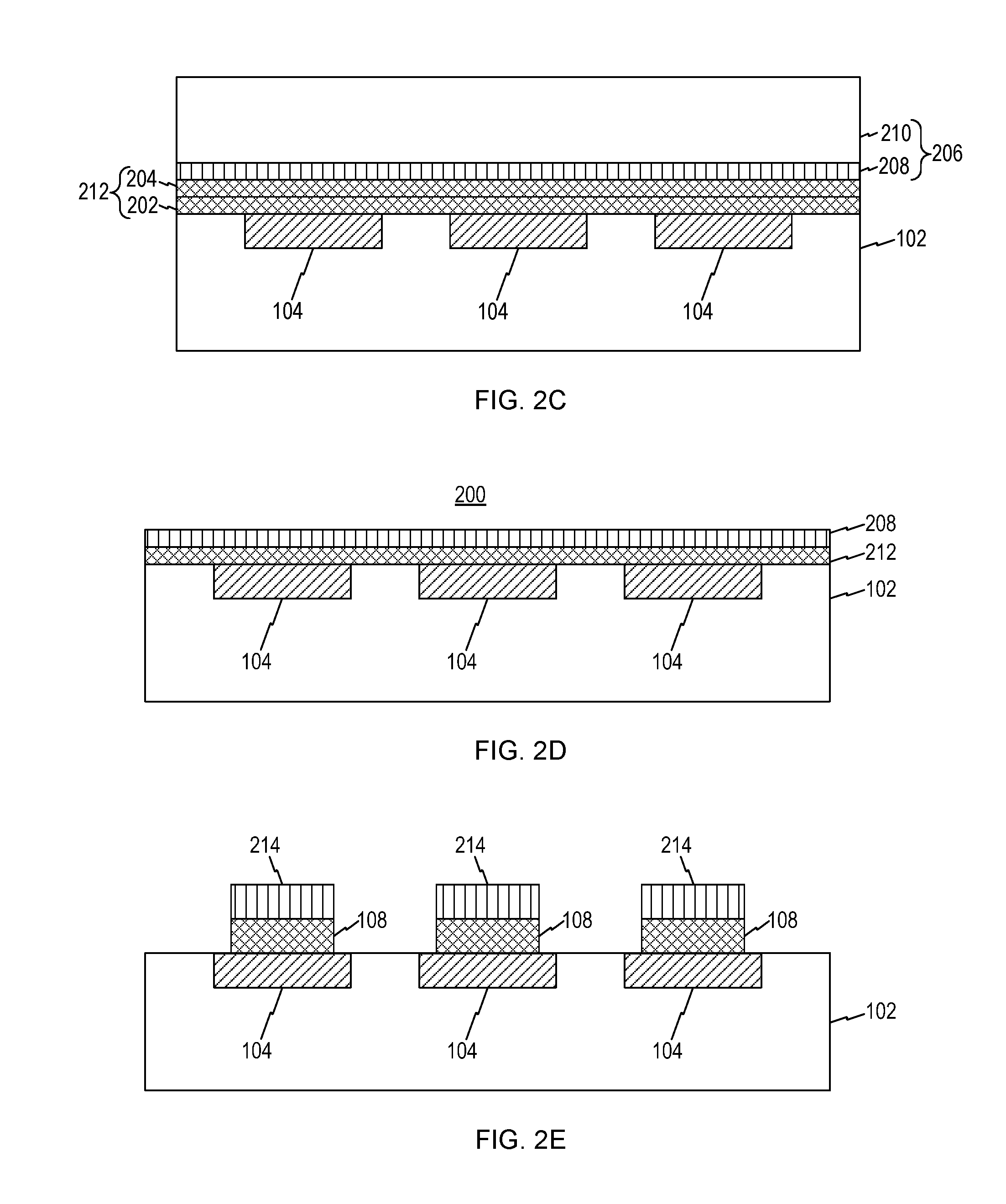
FIGS. 2A-2E schematically show an exemplary process for manufacturing the semiconductor apparatus 100 consistent with embodiments of the present disclosure. As shown in FIG. 2A, a first pre-bonding metal layer 202 is formed over the driver circuit wafer 102, in which the driver circuits 104 were previously formed. The first pre-bonding metal layer 202 includes a bonding material sublayer containing, for example, Sn, Au, Ni, Pd, or Cu, or an alloy thereof. The bonding material sublayer may also include a multi-layer structure having a plurality of layers of one or more bonding materials. In some embodiments, the first pre-bonding metal layer 202 can also include an adhesion sublayer and/or a bonding diffusion barrier sublayer formed between the bonding material sublayer and the driver circuit wafer 102. The adhesion sublayer is configured to enhance the adhesion between the bonding material sublayer and the driver circuit wafer 102, while the bonding diffusion barrier sublayer is configured to prevent or reduce diffusion of the bonding material(s).
Referring to FIG. 2B, separate from the driver circuit wafer 102, a second pre-bonding metal layer 204 is formed over a functional device wafer 206. The second pre-bonding metal layer 204 includes a bonding material sublayer containing, for example, Sn, Au, Ni, Pd, or Cu, or an alloy thereof. The bonding material sublayer may also include a multi-layer structure having a plurality of layers of one or more bonding materials. In some embodiments, the second pre-bonding metal layer 204 can also include an adhesion sublayer and/or a bonding diffusion barrier sublayer formed between the bonding material sublayer and the functional device wafer 206. The adhesion sublayer is configured to enhance the adhesion between the bonding material sublayer and the functional device wafer 206, while the bonding diffusion barrier sublayer is configured to prevent or reduce diffusion of the bonding material(s). In the present disclosure, the functional device wafer 206 is also referred to as an "epi wafer." The functional device wafer 206 includes a functional device epi-structure layer 208, which is also referred to as an "epi-structure layer," epitaxially grown on a growth substrate 210. Depending on the type of the functional device dies 106 to be formed as discussed above, the epi-structure layer 208 can include different epitaxial structures that are suitable for forming the final functional device dies 106. For example, the epi-structure layer 208 can include an opto-electronic device epi-structure layer, such as an LED epi-structure layer, a VCSEL epi-structure layer, or a photodetector epi-structure layer. As another example, the epi-structure layer 208 can include a MEMS epi-structure layer, such as a MEMS sensor epi-structure layer.
The growth substrate 210 can be any substrate that is suitable for the epitaxial growth of the epi-structure layer 208, and is separately provided. For example, if the epi-structure layer 208 includes a GaN-based material, the growth substrate 210 can be a sapphire substrate, such as a patterned sapphire substrate, or can be a SiC substrate. As another example, if the epi-structure layer 208 includes an InP-based material, the growth substrate 210 can be an InP substrate. As a further example, if the epi-structure layer 208 includes a GaAs-based material, the growth substrate 210 can be a GaAs substrate.
Referring to FIG. 2C, the functional device wafer 206 having the second pre-bonding metal layer 204 formed thereon is transferred over and aligned with the driver circuit wafer 102 having the first pre-bonding metal layer 202 formed thereon (shown in FIG. 2A), with the second pre-bonding metal layer 204 facing the first pre-bonding metal layer 202. The functional device wafer 206 is brought into contact with the driver circuit wafer 102, such that the second pre-bonding metal layer 204 contacts and is pressed against the first pre-bonding metal layer 202. A bonding process is conducted to bond the first and second pre-bonding metal layers 202 and 204 to each other to form an unpatterned bonding metal layer 212. In some embodiments, the bonding process includes heating at an elevated temperature such that at least a portion of the first pre-bonding metal layer 202 and at least a portion of the second pre-bonding metal layer 204 melt and the first and second pre-bonding metal layers 202 and 204 are welded to each other. The temperature at which the bonding process is conducted depends on the bonding material(s) used, and can, for example, range from about 230.degree. C. to higher than 350.degree. C. when Au--Sn alloy is used as the bonding material. Other bonding techniques can also be applied as long as they can bond the first and second pre-bonding metal layers 202 and 204 together.
After the first and second pre-bonding metal layers 202 and 204 are bonded together to form the unpatterned bonding metal layer 212, the growth substrate 210 is removed to expose the epi-structure layer 208, as shown in FIG. 2D. The growth substrate 210 can be removed using any suitable physical or chemical substrate removing technique, such as laser lift-off, chemical-mechanical polishing (CMP), or wet etching.
After the growth substrate 210 is removed, the remaining parts constitute another exemplary semiconductor apparatus 200 consistent with embodiments of the present disclosure. That is, the semiconductor apparatus 200 is an intermediate product formed during the process of forming the semiconductor apparatus 100. The semiconductor apparatus 200 includes the driver circuit wafer 102 having the plurality of driver circuits 104 arranged in an array, the unpatterned bonding metal layer 212 formed over the driver circuit wafer 102, and the epi-structure layer 208 formed over the unpatterned bonding metal layer 212. In particular, like the semiconductor apparatus 100, the semiconductor apparatus 200 does not include the growth substrate 210, and therefore the epi-structure layer 208 is exposed to the environment. Different from the semiconductor apparatus 100, the semiconductor apparatus 200 has a horizontally continuous unpatterned bonding metal layer 212 and a horizontally continuous epi-structure layer 208.
Consistent with the present disclosure, after the growth substrate 210 is removed, the epi-structure layer 208 and the unpatterned bonding metal layer 212 can be patterned, for example, using a photo-lithography method, to form functional device mesas 214 and the bonding metal pads 108, respectively, as shown in FIG. 2E. Details of this patterning process are omitted here. In some embodiments, the functional device mesas 214 may be the functional device dies 106, so that the semiconductor apparatus shown in FIG. 2E, which results from the exemplary process described above, is equivalent to the semiconductor apparatus 100 shown in FIG. 1. In some embodiments, further processing may be performed to form the functional device dies 106 from the functional device mesas 214, so as to form the semiconductor apparatus 100 shown in FIG. 1. Moreover, following the patterning process, other processes can be conducted to, for example, form wirings, insulation layers, and/or passivation layers, or to roughen upper surfaces of the functional device dies 106 to improve light extraction in the case of, e.g., LED dies. Descriptions of such processes are also omitted here.
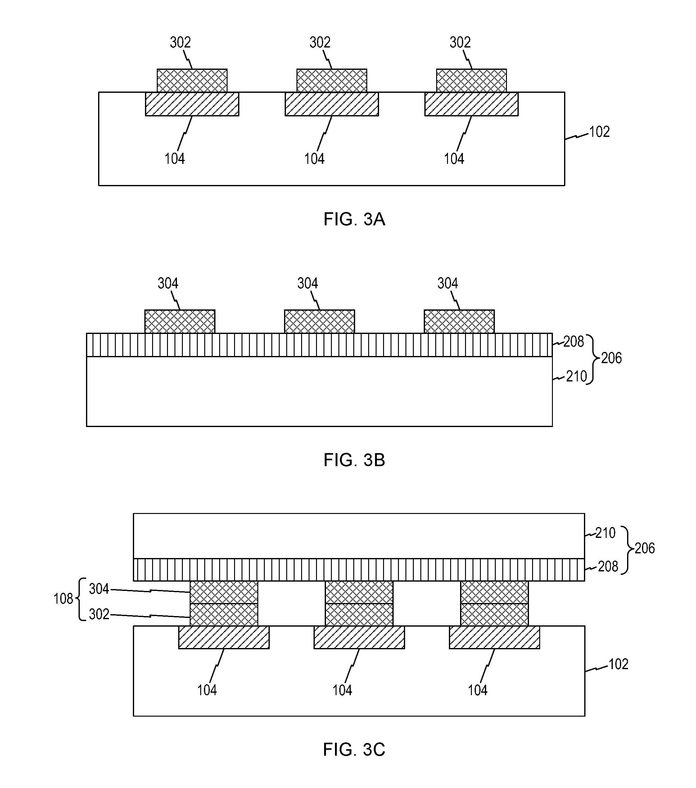
FIGS. 3A-3D schematically show another exemplary process for manufacturing the semiconductor apparatus 100 consistent with embodiments of the present disclosure. In this exemplary process, the steps of forming the first and second pre-bonding metal layers 202 and 204 over the driver circuit wafer 102 and the functional device wafer 206, respectively, are similar to those described above in connection with FIGS. 2A and 2B. Therefore, these two steps are not illustrated again in FIGS. 3A-3D, and the descriptions thereof are omitted.
Referring to FIG. 3A, the first pre-bonding metal layer 202 is patterned to form first pre-bonding metal pads 302. The first pre-bonding metal pads 302 are arranged in an array. Each of the first pre-bonding metal pads 302 corresponds to and is electrically coupled to one of the driver circuits 104. In some embodiments, one first pre-bonding metal pad 302 corresponds to only one driver circuit 104.
According to the present disclosure, the first pre-bonding metal layer 202 can be patterned using any suitable patterning method. For example, the first pre-bonding metal layer 202 can be patterned using a photo-lithography method, during which the first pre-bonding metal layer 202 is etched to remove portions thereof, so as to form the first pre-bonding metal pads 302. Alternatively, the first pre-bonding metal layer 202 can be patterned using a lift-off method. To pattern the first pre-bonding metal layer 202 by the lift-off method, a layer of a material suitable for lift-off (not shown in the drawings), such as a photoresist layer, can be formed over the driver circuit wafer 102 and be patterned before the first pre-bonding metal layer 202 is formed. In this scenario, the first pre-bonding metal layer 202 is formed over the patterned lift-off material layer. The patterned lift-off material layer is then removed along with the portions of the first pre-bonding metal layer 202 that are formed directly on the lift-off material layer. The remaining portions of the first pre-bonding metal layer 202 form the first pre-bonding metal pads 302.
Referring to FIG. 3B, the second pre-bonding metal layer 204 is patterned to form second pre-bonding metal pads 304 that are arranged in an array. Each of the second pre-bonding metal pads 304 corresponds to one of the first pre-bonding metal pads 302, and also corresponds to one of the functional device dies 106 to be formed. Consistent with the present disclosure, the second pre-bonding metal layer 204 can be patterned using a method similar to that used to pattern the first pre-bonding metal layer 202, e.g., the second pre-bonding metal layer 204 can be patterned by etching or lift-off.
After the first and second pre-bonding metal layers 202 and 204 are patterned, the functional device wafer 206 is transferred over and aligned with the driver circuit wafer 102, with the second pre-bonding metal pads 304 facing corresponding ones of the first pre-bonding metal pads 302, as shown in FIG. 3C. Each of the second pre-bonding metal pads 304 is aligned with one of the first pre-bonding metal pads 302. The functional device wafer 206 is brought into contact with the driver circuit wafer 102, such that the second pre-bonding metal pads 304 contact and are pressed against their corresponding first pre-bonding metal pads 302. A bonding process similar to that described with respect to FIG. 2C is conducted to bond the second pre-bonding metal pads 304 with the first pre-bonding metal pads 302 to form the bonding metal pads 108.
After the first and second pre-bonding metal pads 302 and 304 are bonded together to form the bonding metal layer 107 having the bonding metal pads 108, the growth substrate 210 is removed to expose the epi-structure layer 208, as shown in FIG. 3D.
After the growth substrate 210 is removed, the remaining parts constitute another exemplary semiconductor apparatus 300 consistent with embodiments of the present disclosure. That is, the semiconductor apparatus 300 is another intermediate product formed during the process of forming the semiconductor apparatus 100. The semiconductor apparatus 300 includes the driver circuit wafer 102 having the plurality of driver circuits 104 arranged in an array, the bonding metal layer 107 formed over the driver circuit wafer 102 and having the bonding metal pads 108 arranged in an array, and the epi-structure layer 208 formed over the bonding metal layer 107. In particular, like the semiconductor apparatus 100, the semiconductor apparatus 300 does not include the growth substrate 210, and therefore the epi-structure layer 208 is exposed to the environment. Different from the semiconductor apparatus 100, the semiconductor apparatus 300 has a horizontally continuous epi-structure layer 208.
Consistent with the present disclosure, after the growth substrate 210 is removed, the epi-structure layer 208 can be patterned, for example, using a photo-lithography method, to form the functional device mesas 214, resulting in a semiconductor apparatus similar to that shown in FIG. 2E, which is thus not shown again. Details of patterning the epi-structure layer 208 are omitted here.
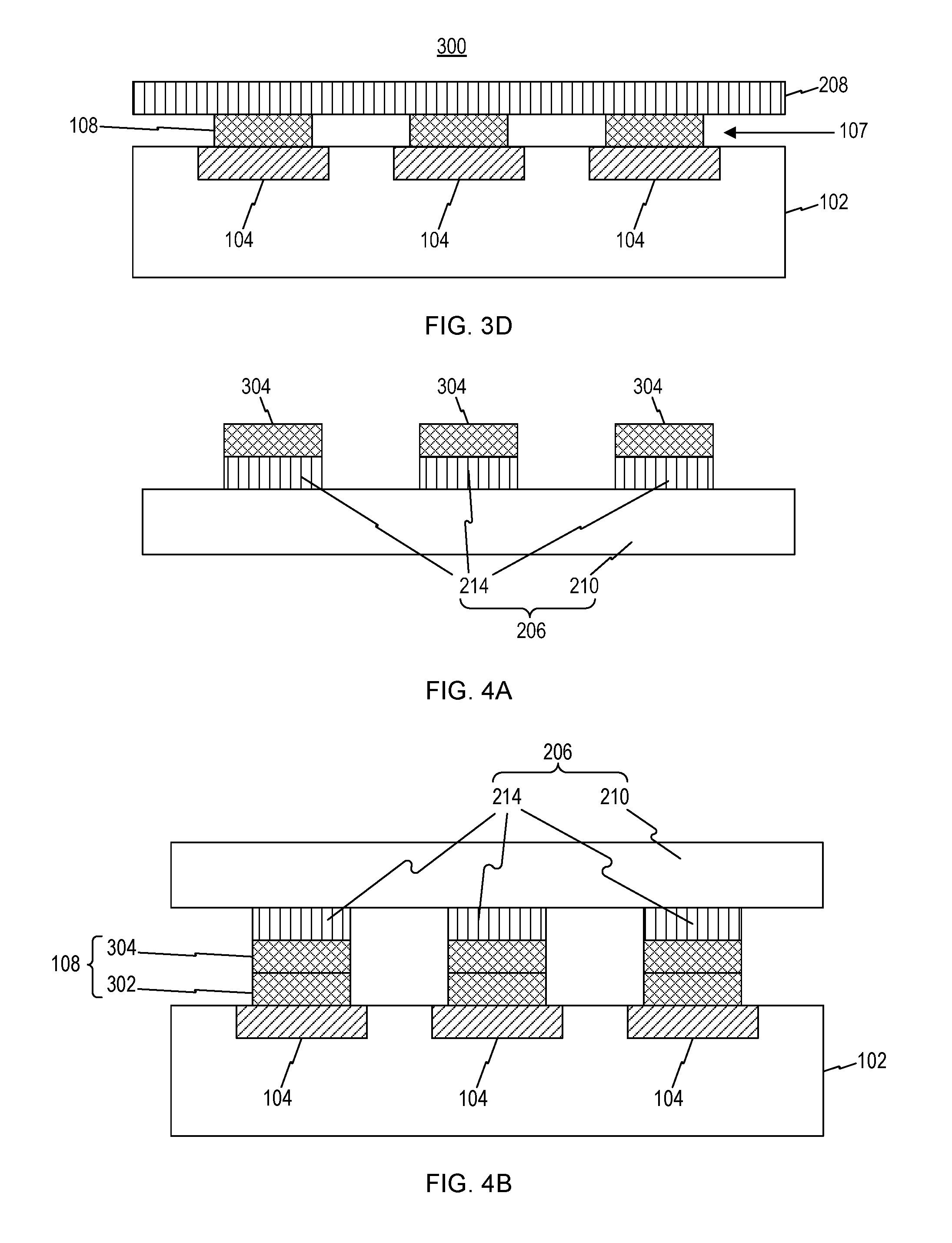
FIGS. 4A and 4B schematically show another exemplary process for manufacturing the semiconductor apparatus 100 consistent with embodiments of the present disclosure. In this exemplary process, the steps of forming the first and second pre-bonding metal layers 202 and 204, and the steps of patterning the first and second pre-bonding metal layers 202 and 204 to form the first and second pre-bonding metal pads 302 and 304 are similar to those described above in connection with FIGS. 2A, 2B, 3A, and 3B. Therefore, these steps are not illustrated again in FIGS. 4A and 4B, and the descriptions thereof are omitted.
Referring to FIG. 4A, the epi-structure layer 208 is patterned to form the functional device mesas 214. For example, the epi-structure layer 208 can be patterned by etching using the second pre-bonding metal pads 304 as masks. As another example, the epi-structure layer 208 can be patterned by a separate photolithography process, which includes, e.g., forming a photoresist layer over the epi-structure layer 208 and the second pre-bonding metal pads 304, patterning the photoresist layer to remove portions of the photoresist layer with remaining portions over the second pre-bonding metal pads 304, and then etching the epi-structure layer 208 using the remaining portions of the photoresist layer as masks. Each of the remaining portions of the photoresist layer may have a larger area than the corresponding second pre-bonding metal pad 304, and thus each of the functional device mesas 214 formed by the above second exemplary process may have a larger area than the corresponding second pre-bonding metal pad 304, although the larger area is not explicitly illustrated in FIG. 4A.
Then, as shown in FIG. 4B, the functional device wafer 206 is bonded with the driver circuit wafer 102. A bonding process similar to that described above in connection with FIG. 3C is conducted to bond the functional device wafer 206 and the driver circuit wafer 102.
After the functional device wafer 206 and the driver circuit wafer 102 are bonded together, the growth substrate 210 is removed to expose the functional device mesas 214, resulting in a semiconductor apparatus similar to that shown in FIG. 2E, which is thus not shown again.
In the exemplary process described above in connection with FIGS. 4A and 4B, the second pre-bonding metal layer 204 is first formed and patterned to form the second pre-bonding metal pads, and the epi-structure layer 208 is patterned thereafter. In some embodiments, the epi-structure layer 208 can be patterned before the second pre-bonding metal layer 204 is formed over the functional device wafer 206. This exemplary process is described below in connection with FIGS. 5A and 5B.
In this exemplary process, the steps of forming and patterning the first pre-bonding metal layer 202 are similar to those described above in connection with FIGS. 2A and 3A. Therefore, these steps are not illustrated again in FIGS. 5A and 5B, and the descriptions thereof are omitted.
Referring to FIG. 5A, the epi-structure layer 208 is patterned, for example, using a photolithography method, to form the functional device mesas 214. Then, as shown in FIG. 5B, the second pre-bonding metal pads 304 are formed over the functional device mesas 214. For example, forming the second pre-bonding metal pads 304 can include first depositing the pre-bonding metal layer 204 (not shown in FIG. 5B) and then patterning the pre-bonding metal layer 204 to form the second pre-bonding metal pads 304. The subsequent processing steps of this exemplary process are similar to those described above in connection with FIGS. 4B and 4C, and thus are not illustrated and descriptions thereof are omitted.
In the exemplary process described above in connection with FIGS. 2A-2E, both the first and second pre-bonding metal layers 202 and 204 are patterned after the driver circuit wafer 102 and the functional device wafer 206 are bonded together, while in the exemplary processes described above in connection with FIGS. 3A-5B, both the first and second pre-bonding metal layers 202 and 204 are patterned before the driver circuit wafer 102 and the functional device wafer 206 are bonded together. In other embodiments, either one of the first pre-bonding metal layer 202 or the second pre-bonding metal layer 204 can be patterned before the bonding process and the other one can be patterned after the bonding process.
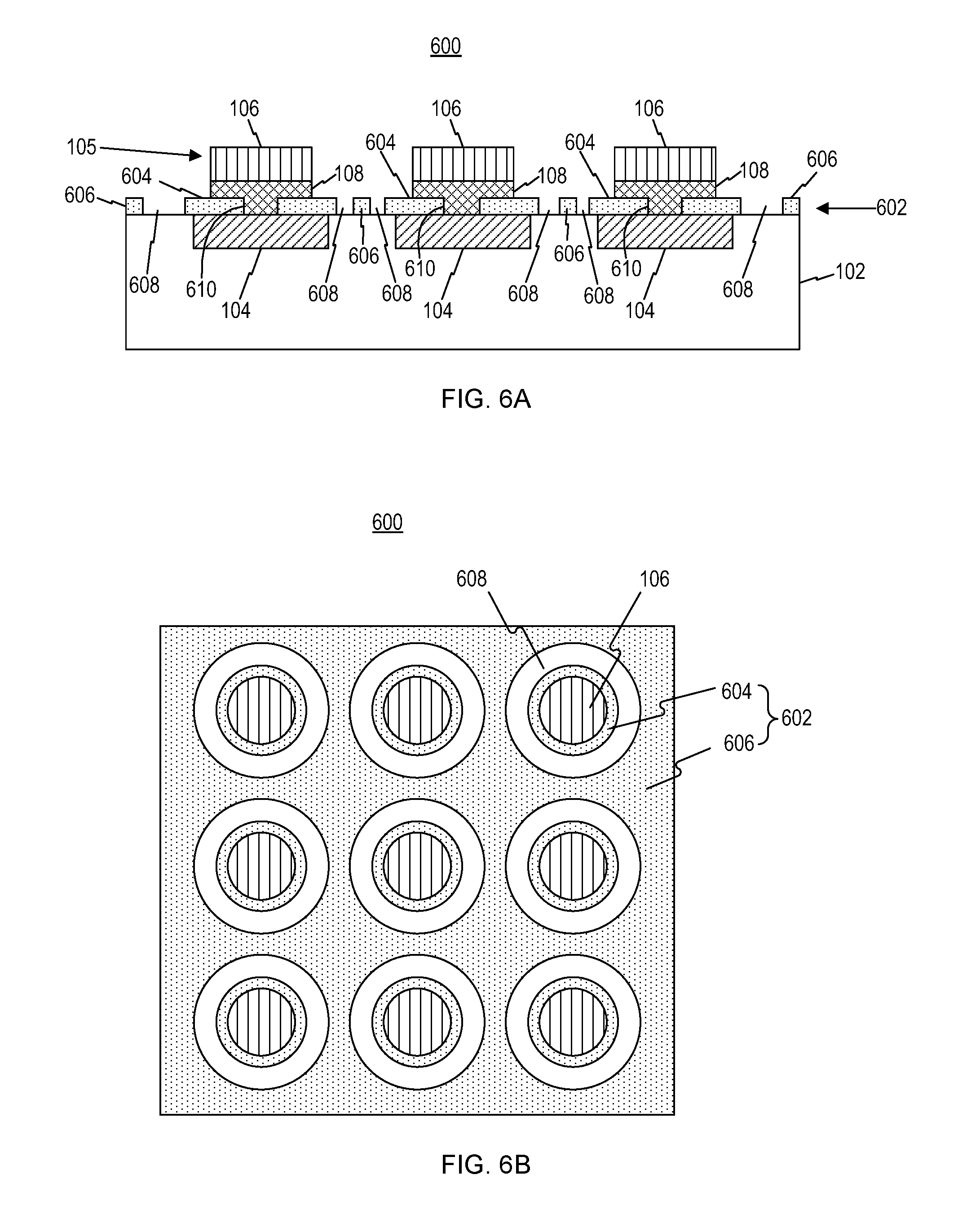
In the exemplary processes described above in connection with FIGS. 3A-5B, the first and second pre-bonding metal pads 302 and 304 are formed before the bonding process. The first pre-bonding metal pads 302 are physically and electrically separated from each other. Similarly, the second pre-bonding metal pads 304 are physically and electrically separated from each other. However, during the bonding process, portions of the first and second pre-bonding metal pads 302 and 304 may melt and, under the pressure exerted during the bonding process, the melt metal from the first and/or second pre-bonding metal pads 302, 304 may flow along the surface of the driver circuit wafer 102 and reach neighboring first and/or second pre-bonding metal pads 302, 304, causing a short circuit in the resulting semiconductor apparatus. To avoid this issue, structures preventing the melt metal from reaching neighboring first and/or second pre-bonding metal pads 302, 304 can be formed in the semiconductor apparatus. FIGS. 6A and 6B schematically show an exemplary semiconductor apparatus 600 having such structures consistent with embodiments of the present disclosure.
FIG. 6A is a cross-sectional view schematically showing the semiconductor apparatus 600, which is similar to the semiconductor apparatus 100, except that the semiconductor apparatus 600 further includes a dielectric isolation layer 602 arranged between the driver circuit wafer 102 and the functional device epi-layer 105. The dielectric isolation layer 602 includes first protrusion structures 604 and second protrusion structures 606 surrounding the first protrusion structures 604. As shown in FIG. 6A, each of the first protrusion structures 604 is formed over one of the driver circuits 104, and each of the bonding metal pads 108 is formed over one of the first protrusion structures 604. That is, each of the first protrusion structures 604 "holds" one bonding metal pad 108, and thus the first protrusion structures 604 are also referred to in this disclosure as "bonding metal pad plateaus" or "solder pad plateaus."
FIG. 6B is a plan view of the semiconductor apparatus 600, showing the second protrusion structures 606 surrounding each of the first protrusion structures 604 and separating neighboring first protrusion structures 604 from each other. As shown in FIGS. 6A and 6B, each of the first protrusion structures 604 and the corresponding neighboring second protrusion structures 606 define a recess 608 surrounding the first protrusion structure 604. During the bonding process, if melt bonding metal outflows from the first protrusion structures 604, it is contained in the recesses 608 and confined by the second protrusion structures 606, and does not reach neighboring bonding metal pads 108. Thus, the recesses 608 are also referred to in this disclosure as "bonding metal reservoirs" or "solder reservoirs," and the second protrusion structures 606 are also referred to as "bonding metal confinement dams" or "solder confinement dams."
Referring again to FIG. 6A, each of the first protrusion structures 604 includes a through hole 610 formed between the upper surface and the lower surface of that first protrusion structure 604. At least a portion of the corresponding bonding metal pad 108 is formed in the through hole 610, forming an electrical path to the corresponding driver circuit 104 located beneath the first protrusion structure 604.
Consistent with the present disclosure, the dielectric isolation layer 602 can also be included in the semiconductor apparatus 300, in a manner similar to that shown in FIGS. 6A and 6B and described above.
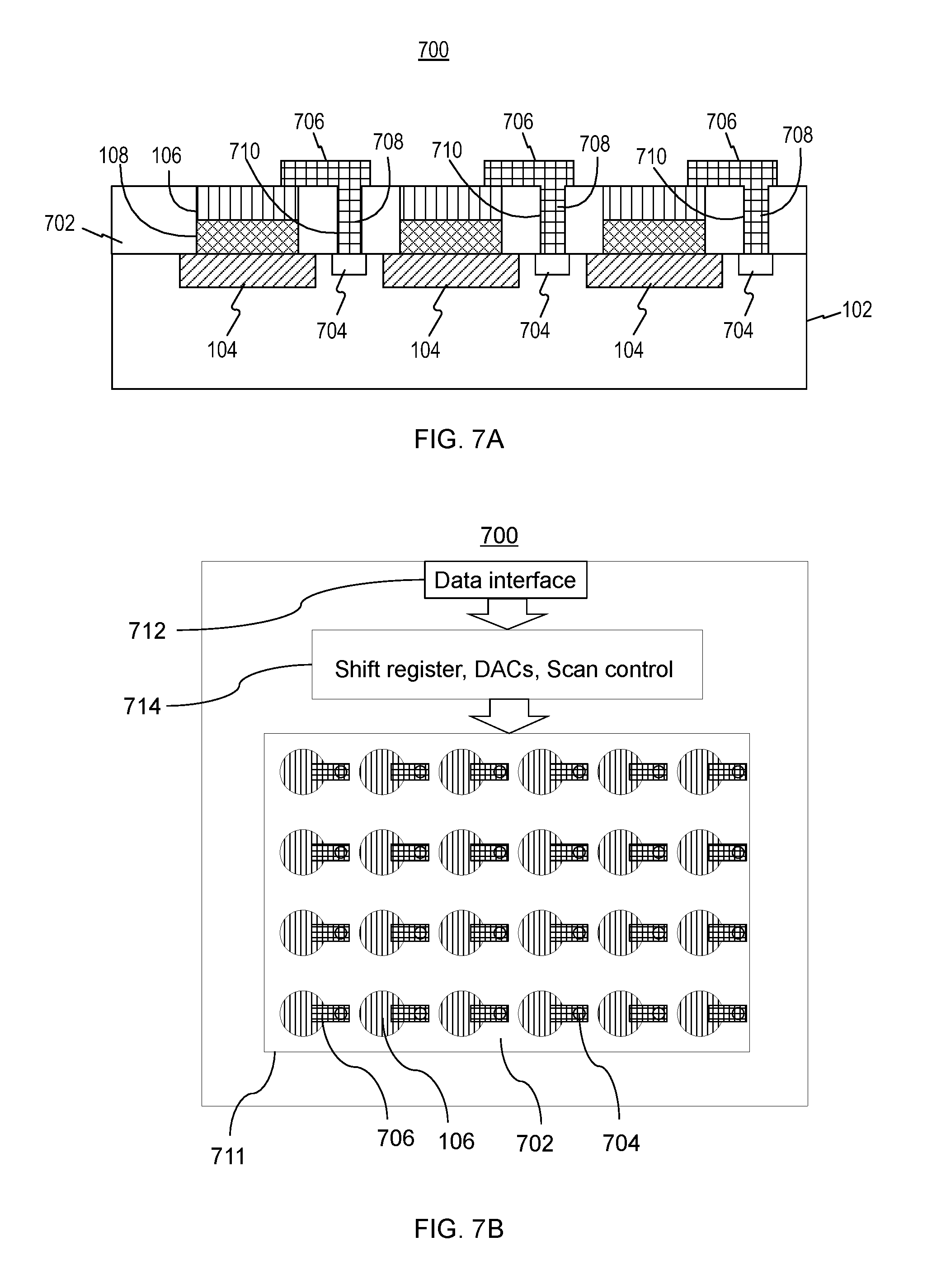
As described above, the functional device dies 106 are spatially separated from each other. In some embodiments, an isolation layer may be formed between the functional device dies 106. FIGS. 7A and 7B schematically show another exemplary semiconductor apparatus 700 consistent with embodiments of the present disclosure. The semiconductor apparatus 700 is similar to the semiconductor apparatus 100, except that the semiconductor apparatus 700 further includes an isolation layer 702 formed between the functional device dies 106. FIG. 7A is a cross-sectional view schematically showing the semiconductor apparatus 700. In the example shown in FIG. 7A, the top surface of the isolation layer 702 is flat or approximately flat, and is flush or approximately flush with top surfaces of the functional device dies 106. However, the isolation layer 702 can be higher or lower than the functional device dies 106. Consistent with the present disclosure, the isolation layer 702 can be formed of, for example, a dielectric material to improve the electrical isolation between neighboring functional device dies 106.
As noted above, the functional device dies 106 can be opto-electronic device dies that can emit or absorb light of a certain wavelength. The spatial separation among the opto-electronic device dies can ensure good optical isolation between neighboring opto-electronic device dies. Such an optical isolation can, for example, reduce cross-talk between the neighboring opto-electronic device dies. The optical isolation can be further improved by choosing a suitable material for the isolation layer 702 in the semiconductor apparatus 700. That is, the isolation layer 702 can be formed of a material that further reduces light transmission between neighboring opto-electronic device dies. For example, the material can be a light absorptive material that can absorb light having a wavelength associated with an opto-electronic device die, such as an LED die. In the present disclosure, a wavelength or a wavelength range associated with a die or a layer refers to a wavelength or a wavelength range of light emitted or absorbed by the die or the layer. The absorptive material can be a material having a lower transparency than air. In some embodiments, the isolation layer 702 is formed of a material that is non-transparent to light having a wavelength associated with the opto-electronic device dies. For example, if the opto-electronic device dies include LED dies that emit blue light, a material non-transparent to blue light can be chosen to form the isolation layer 702. Alternatively, the isolation layer 702 can include a reflective material that can reflect light having a wavelength associated with an opto-electronic device die, such as an LED die. For example, the reflective material may reflect the light emitted by an LED die back to that LED die. The reduced-transparency (absorptive) material or the reflective material increases the optical confinement of individual opto-electronic device dies and enhances the optical isolation.
In some embodiments, in the scenario that the functional device dies 106 include opto-electronic device dies, the isolation layer 702 does not need to completely fill in the space between neighboring opto-electronic device dies, but can be formed as conformal layers on the sidewalls of the opto-electronic device dies, especially if the isolation layer 702 is formed of a reflective material.
In some embodiments, as shown in FIG. 7A, the semiconductor apparatus 700 further includes a plurality of ground pads 704, also referred to as "ground electrodes," formed in a dielectric layer (not shown) in the driver circuit wafer 102. Each of the ground pads 704 is associated with one of the driver circuits 104 and provides a ground level to the associated driver circuit 104. The ground pads 704 are electrically coupled to each other and to a common ground (not shown) of the semiconductor apparatus 700.
As shown in FIG. 7A, the semiconductor apparatus 700 further includes a plurality of metal wirings 706 formed over the isolation layer 702. Each of the metal wirings 706 contacts a portion of the top surface of a corresponding functional device die 106, and is electrically coupled to the corresponding functional device die 106. For example, each of the metal wirings 706 can be in direct contact with the uppermost epitaxial layer in the corresponding functional device die 106. Moreover, each of the metal wirings 706 includes a plug portion 708 formed in a wiring through hole 710 formed in the isolation layer 702. Each of the metal wirings 706 contacts and is electrically coupled to a corresponding ground pad 704 via the plug portion 708 of the metal wiring 706. Thus, the metal wirings 706 form a cross-connected metal layer.
FIG. 7B is a plan view of the semiconductor apparatus 700, schematically showing the wiring of the semiconductor apparatus 700 in a functional device area 711 containing the functional device dies 106. Moreover, as shown in FIG. 7B, the semiconductor apparatus 700 further includes a data interface 712 for receiving and/or outputting data, e.g., input data used to control the operations of the functional device dies 106 or output data generated by the functional device dies 106. The semiconductor apparatus 700 also includes a control portion 714 coupled between the data interface 712 and the functional device area 711. The control portion 712 may include, for example, one or more shift registers, one or more digital-analog converters (DACs), and/or one or more scan controllers.
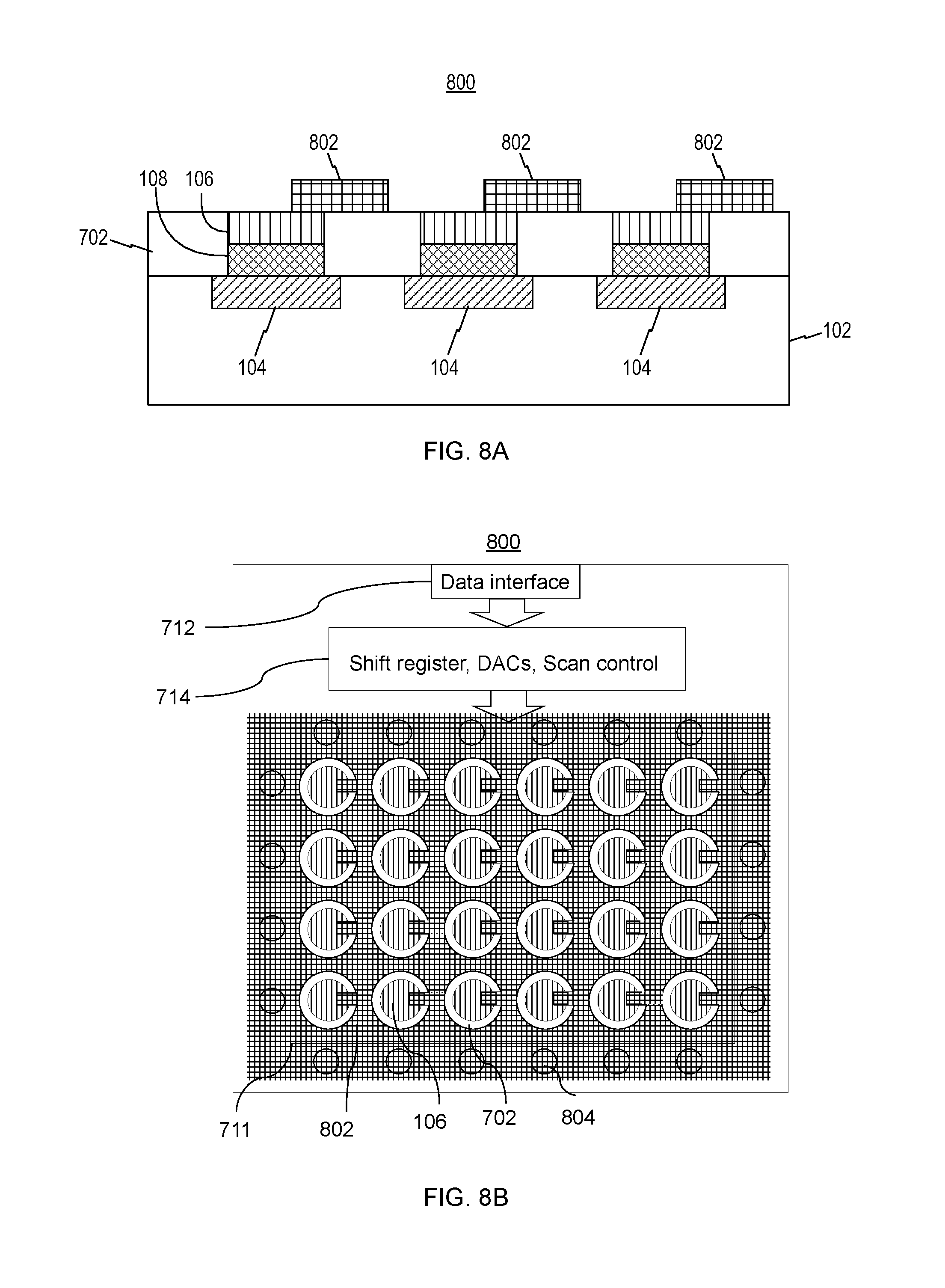
In the semiconductor apparatus 700, the metal wirings 706 contact and are electrically coupled to the ground pads 704, each of which is associated with one of the driver circuits 104. FIGS. 8A and 8B are cross-sectional and plan views, respectively, of another exemplary semiconductor apparatus 800 consistent with embodiments of the present disclosure. As shown in FIGS. 8A and 8B, the semiconductor apparatus 800 includes a continuous wiring layer 802 formed over the isolation layer 702. The wiring layer 802 contacts and is electrically coupled to each of the functional device dies 106. For example, the wiring layer 802 can be in direct contact with the uppermost epitaxial layer in each of the functional device dies 106. The wiring layer 802 is further electrically coupled to ground pads 804 formed in a peripheral region surrounding the functional device area 711, as shown in FIG. 8B.
In some embodiments, a semiconductor apparatus consistent with the present disclosure does not include the above-described isolation layer 702, but instead has a conformal passivation layer formed all over the semiconductor apparatus. FIG. 9 is a cross-sectional view schematically showing such an exemplary semiconductor apparatus 900. The semiconductor apparatus 900 is similar to the semiconductor apparatus 100, except that the semiconductor apparatus 900 further includes a passivation layer 902. As shown in FIG. 9, the passivation layer 902 is conformally formed over the functional device dies 106, the bonding metal pads 108, and the exposed area of the driver circuit wafer 102. For example, the passivation layer 902 can be in direct contact with the uppermost epitaxial layer in each of the functional device dies 106.
In some embodiments, as shown in FIG. 9, the semiconductor apparatus 900, like the semiconductor apparatus 700, also includes the ground pads 704 formed in a dielectric layer (not shown) in the driver circuit wafer 102. Functional device contact openings 904 and ground contact openings 906 are formed through the passivation layer 902 in areas over the functional device dies 106 and the ground pads 704, respectively. Metal wirings 908 are formed over the passivation layer 902, each of which is electrically coupled to the upper surface of one of the functional device dies 106 and the corresponding ground pad 704.
In the above-described drawings, the functional device epi-layer 105, the bonding metal layer 107, and the driver circuit wafer 102 are shown one over another. In some embodiments, the semiconductor apparatus consistent with the present disclosure may further include one or more electrode layers. For example, the semiconductor apparatus may include a device side electrode layer formed between the functional device epi-layer 105 and the bonding metal layer 107. The device side electrode layer can be formed of one or more conducting materials, and include a plurality of device side electrodes. Each of the device side electrodes corresponds to one of the functional device dies 106 and one of the bonding metal pads 108, and provides an electrical path between the corresponding functional device die 106 and bonding metal pad 108.
The material(s) forming the device side electrode layer may be different for different types of functional device dies 106. For example, if the functional device dies 106 include LED dies, the device side electrode layer can include a reflecting layer formed over the bonding metal layer 107 and a transparent conducting material layer formed over the reflecting layer. The reflecting layer reflects the light generated by the LED dies, increasing the efficiency of the LED dies, and may include a reflecting material, such as Sn, aluminum (Al), silver (Ag), rhodium (Rd), copper (Cu), or Au, or a reflecting structure, such as DBR.
In some embodiments, the semiconductor apparatus may additionally or alternatively include a driver side electrode layer formed between the bonding metal layer 107 and the driver circuit wafer 102. The driver side electrode layer can be formed of one or more conducting materials, and include a plurality of driver side electrodes. Each of the driver side electrodes corresponds to one of the bonding metal pads 108 and one of the driver circuits 104, and provides an electrical path between the corresponding bonding metal pad 108 and driver circuit 104. Consistent with the present disclosure, the driver side electrode layer can be formed on the driver circuit wafer 102, or at least partially in a dielectric layer formed over or in the driver circuit wafer 102.
As discussed above, the semiconductor apparatus consistent with the present disclosure can include opto-electronic device dies and thus be an opto-electronic apparatus. The opto-electronic device dies in the same opto-electronic apparatus can have a similar structure and are associated with light having a similar wavelength or a similar wavelength range. In some embodiments, additional optical elements having different associated wavelengths or wavelength ranges may be formed in the opto-electronic apparatus for different opto-electronic device dies.
FIG. 10 is a cross-sectional view schematically showing an exemplary opto-electronic apparatus 1000 consistent with embodiments of the present disclosure. The opto-electronic apparatus 1000 includes the driver circuit wafer 102 having the driver circuits 104, the bonding metal layer 107 formed over the driver circuit wafer 102 and having the bonding metal pads 108, and an opto-electronic epi-layer 1005 formed over the bonding metal layer 107 and having a plurality of opto-electronic device dies 1006. The opto-electronic apparatus 1000 further includes a first optical element 1010a, a second optical element 1010b, and a third optical element 1010c. As shown in FIG. 10, each of the first, second, and third optical elements 1010a, 1010b, and 1010c is formed over one of the opto-electronic device dies 1006. In other embodiments, each of the first, second, and third optical elements 1010a, 1010b, and 1010c may be formed over one or more of the opto-electronic device dies 1006. The first, second, and third optical elements 1010a, 1010b, and 1010c are associated with a first wavelength or a first wavelength range, a second wavelength or a second wavelength range, and a third wavelength or a third wavelength range, respectively, which may be different from each other. In the example shown in FIG. 10, the first, second, and third optical elements 1010a, 1010b, and 1010c are formed to cover all exposed surfaces of the corresponding opto-electronic device dies 1006. In other embodiments, the first, second, and third optical elements 1010a, 1010b, and 1010c can be formed, for example, to only over the upper surfaces of the corresponding opto-electronic device dies 1006.
Depending on the type of the opto-electronic device dies 1006, the first, second, and third optical elements 1010a, 1010b, and 1010c can be different types of optical elements. For example, the opto-electronic device dies 1006 are LED dies, such as GaN-based ultra-violet (UV) LED dies. In this scenario, the first, second, and third optical elements 1010a, 1010b, and 1010c can be phosphor layers containing different types of phosphors. For example, the first optical element 1010a can contain blue phosphors, the second optical element 1010b can contain green phosphors, and the third optical element 1010c can contain red phosphors. As such, UV light emitted by the LED dies can be converted into different colors. Such an opto-electronic apparatus can be used, for example, as a full-color display panel or as a white-light illumination panel.
As another example, the opto-electronic device dies 1006 are photodetector dies, such as Si-based photodetector dies or III-V material-based photodetector dies. In this scenario, the first, second, and third optical elements 1010a, 1010b, and 1010c can be filter layers that allow light of different wavelengths or different wavelength ranges to pass through. For example, the first optical element 1010a can be a filter layer that allows blue light to pass through, the second optical element 1010b can be a filter layer that allows green light to pass through, and the third optical element 1010c can be a filter layer that allows red light to pass through. Such an opto-electronic apparatus can be used, for example, as a full-color sensor used in a digital camera.
As an alternative to the examples described above, the opto-electronic device dies themselves can be configured in such a manner that they are associated with different wavelengths or different wavelength ranges. FIG. 11 is a cross-sectional view schematically showing another exemplary opto-electronic apparatus 1100 consistent with embodiments of the present disclosure. The opto-electronic apparatus 1100 includes the driver circuit wafer 102 having the driver circuits 104, the bonding metal layer 107 formed over the driver circuit wafer 102 and having the bonding metal pads 108, and an opto-electronic epi-layer 1105 formed over the bonding metal layer 107 and having a plurality of opto-electronic device dies 1106. The opto-electronic device dies 1106 include a first opto-electronic device die 1106a associated with a first wavelength or a first wavelength range, a second opto-electronic device die 1106b associated with a second wavelength or a second wavelength range, and a third opto-electronic device die 1106c associated with a third wavelength or a third wavelength range. The first, second, and third wavelengths, or the first, second, and third wavelength ranges, can be different from each other.
FIG. 11 only shows one first opto-electronic device die 1106a, one second opto-electronic device die 1106b, and one third opto-electronic device die 1106c. However, consistent with the present disclosure, the opto-electronic apparatus 1100 can have more than one first opto-electronic device die 1106a, more than one second opto-electronic device die 1106b, and/or more than one third opto-electronic device die 1106c.
In some embodiments, the opto-electronic device dies 1106a, 1106b, and 1106c are light-emitting dies such as LED dies that emit light of different wavelengths or different wavelength ranges. For example, the first, second, and third opto-electronic device dies 1106a, 1106b, and 1106c can be red, green, and blue LED dies, respectively, or be red, blue, and green LED dies, respectively, or be green, red, and blue LED dies, respectively, or be green, blue, and red LED dies, respectively, or be blue, red, and green LED dies, respectively, or be blue, green, and red LED dies, respectively. Such an opto-electronic apparatus can also be used, for example, as a full-color display panel or as a white-light illumination panel.
In some embodiments, the opto-electronic device dies 1106a, 1106b, and 1106c are light-absorbing dies such as photodetector dies that absorb light of different wavelengths or different wavelength ranges. For example, the first opto-electronic device die 1106a can be a photodetector die detecting blue light, the second opto-electronic device die 1106b can be a photodetector dies detecting green light, and the third opto-electronic device die 1106c can be a photodetector die detecting red light. Such an opto-electronic apparatus can also be used, for example, as a full-color sensor used in a digital camera.
As shown in FIG. 11, the first opto-electronic device die 1106a includes a first active layer 1110a associated with the first wavelength or the first wavelength range. The second opto-electronic device die 1106b includes a second active layer 1110b associated with the second wavelength or the second wavelength range, and formed over a first dummy layer 1110a'. The third opto-electronic device die 1106c includes a third active layer 1110c associated with the third wavelength or the third wavelength range, and formed over a second dummy layer 1110b'. The second dummy layer 1110b' is in turn formed over a third dummy layer 1110a''. Consistent with the present disclosure, the first active layer 1110a, the first dummy layer 1110a', and the third dummy layer 1110a'' have a similar material structure. Similarly, the second active layer 1110b and the second dummy layer 1110b' have a similar material structure.
As shown in FIG. 11, the first, second, and third opto-electronic device dies 1106a, 1106b, and 1106c are bonded to the driver circuit wafer 102 through the bonding metal pads 108 of the bonding metal layer 107. In the embodiments described here in connection with FIG. 11 and below in connection with FIGS. 12A-12K, the bonding metal layer 107 is also referred to as "first bonding metal layer 107" and the bonding metal pads 108 are also referred to as "first bonding metal pads 108." The opto-electronic apparatus 1100 further includes a second bonding metal layer 1112 having a plurality of second bonding metal pads 1114 and a third bonding metal layer 1116 having a plurality of third bonding metal pads 1118 (one of which is shown in FIG. 11). The second active layer 1110b is bonded to the first dummy layer 1110a' through one of the second bonding metal pads 1114. The second dummy layer 1110b' is bonded to the third dummy layer 1110a'' through another one of the second bonding metal pads 1114. Further the third active layer 1110c is bonded to the second dummy layer 1110b' through one of the third bonding metal pads 1118.
FIGS. 12A-12K schematically show an exemplary process for manufacturing the opto-electronic apparatus 1100 consistent with embodiments of the present disclosure. In this exemplary process, the step for forming the first pre-bonding metal layer 202 over the driver circuit wafer 102 is similar to that described above in connection with FIG. 2A. Therefore, this step is not illustrated again in FIGS. 12A-12K, and the description thereof is omitted.
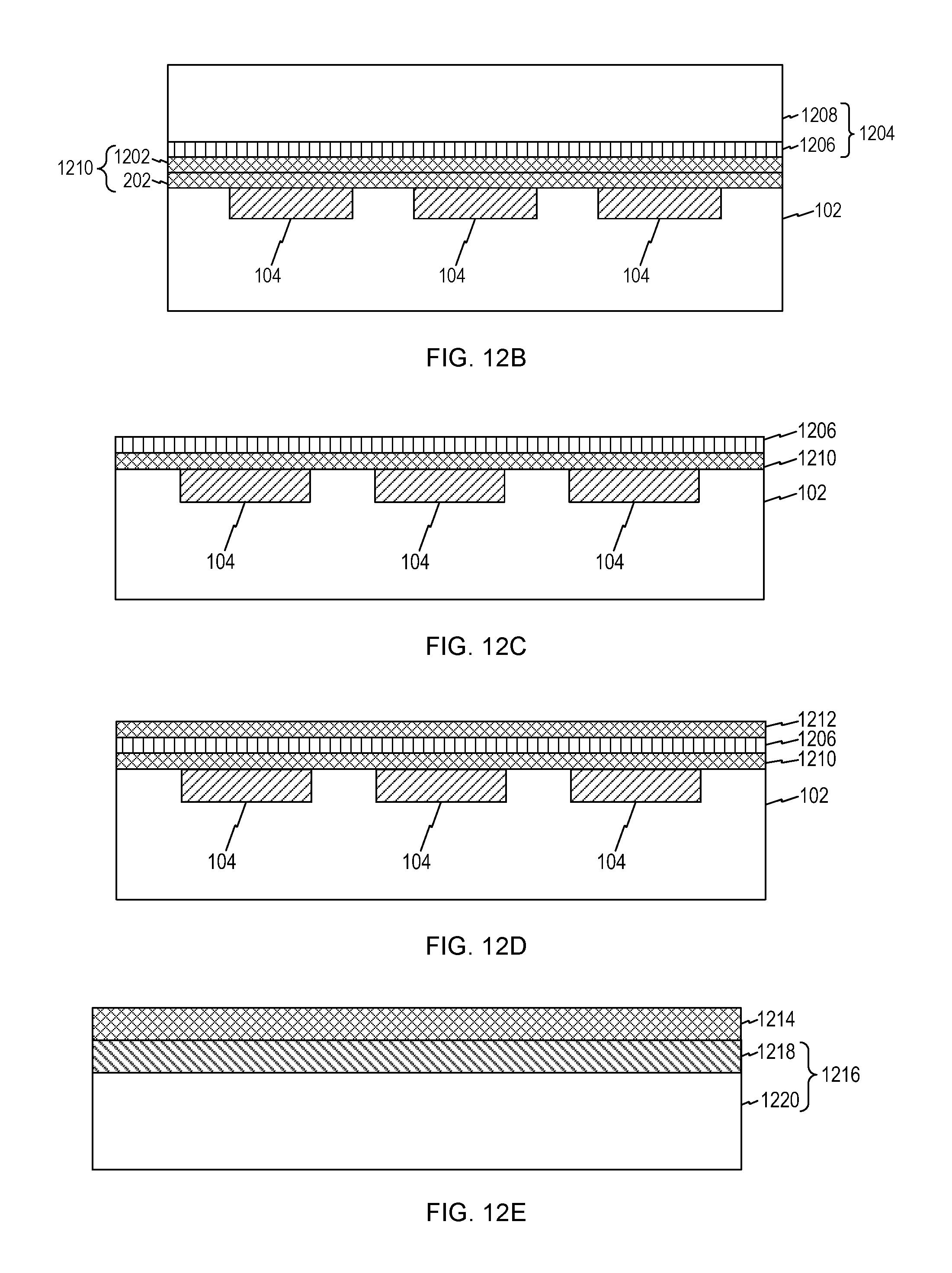
Referring to FIG. 12A, a second pre-bonding metal layer 1202 is formed over a first opto-electronic device wafer 1204. The first opto-electronic device wafer 1204 includes a first opto-electronic device epi-structure layer 1206 epitaxially grown on a first growth substrate 1208. Next, as shown in FIG. 12B, the first opto-electronic device wafer 1204 is bonded to the driver circuit wafer 102, with the second pre-bonding metal layer 1202 and the first pre-bonding metal layer 202 being bonded together to form a first unpatterned bonding metal layer 1210. Thereafter, as shown in FIG. 12C, the first growth substrate 1208 is removed to expose the first opto-electronic device epi-structure layer 1206.
Referring to FIG. 12D, a third pre-bonding metal layer 1212 is formed over the first opto-electronic device epi-structure layer 1206. Also, as shown in FIG. 12E, a fourth pre-bonding metal layer 1214 is formed over a second opto-electronic device wafer 1216, which includes a second opto-electronic device epi-structure layer 1218 epitaxially grown on a second growth substrate 1220. Next, as shown in FIG. 12F, the second opto-electronic device wafer 1216 is bonded to the first opto-electronic device epi-structure layer 1206, with the fourth pre-bonding metal layer 1214 and the third pre-bonding metal layer 1212 being bonded together to form a second unpatterned bonding metal layer 1222. Thereafter, as shown in FIG. 12G, the second growth substrate 1220 is removed to expose the second opto-electronic device epi-structure layer 1218.
Referring to FIG. 12H, a fifth pre-bonding metal layer 1224 is formed over the second opto-electronic device epi-structure layer 1218. Also, as shown in FIG. 12I, a sixth pre-bonding metal layer 1226 is formed over a third opto-electronic device wafer 1228, which includes a third opto-electronic device epi-structure layer 1230 epitaxially grown on a third growth substrate 1232. Next, as shown in FIG. 12J, the third opto-electronic device wafer 1228 is bonded to the second opto-electronic device epi-structure layer 1218, with the sixth pre-bonding metal layer 1226 and the fifth pre-bonding metal layer 1224 being bonded together to form a third unpatterned bonding metal layer 1234. Thereafter, as shown in FIG. 12K, the third growth substrate 1232 is removed to expose the third opto-electronic device epi-structure layer 1230.
After the third growth substrate 1232 is removed, the remaining parts constitute another exemplary semiconductor apparatus 1200 consistent with embodiments of the present disclosure. That is, the semiconductor apparatus 1200 is an intermediate product formed during the process of forming the semiconductor apparatus 1100. As shown in FIG. 12, the semiconductor apparatus 1200 includes the driver circuit wafer 102 having the plurality of driver circuits 104 arranged in an array, the first unpatterned bonding metal layer 1210 formed over the driver circuit wafer 102, the first opto-electronic device epi-structure layer 1206 formed over the first unpatterned bonding metal layer 1210, the second unpatterned bonding metal layer 1222 formed over the first opto-electronic device epi-structure layer 1206, the second opto-electronic device epi-structure layer 1218 formed over the second unpatterned bonding metal layer 1222, the third unpatterned bonding metal layer 1234 formed over the second opto-electronic device epi-structure layer 1218, and the third opto-electronic device epi-structure layer 1230 formed over the third unpatterned bonding metal layer 1234. In particular, like the semiconductor apparatus 1100, the semiconductor apparatus 1200 does not include any growth substrate, and therefore the third opto-electronic device epi-structure layer 1230 is exposed to the environment. Different from the semiconductor apparatus 1100, the semiconductor apparatus 1200 has horizontally continuous first, second, and third unpatterned bonding metal layers 1210, 1222, and 1234, and horizontally continuous first, second, and third opto-electronic device epi-structure layers 1206, 1218, and 1230.
According to the present disclosure, after the first, second, and third opto-electronic device epi-structure layers 1206, 1218, and 1230 are bonded onto the driver circuit wafer 102, subsequent processes including patterning the opto-electronic device epi-structure layers 1206, 1218, and 1230, and the first, second, and third unpatterned bonding metal layers 1210, 1222, and 1234, are performed to form the opto-electronic apparatus 1110 shown in FIG. 11.
In the exemplary process described above in connection with FIGS. 12A-12K, the first, second, and third opto-electronic device epi-structure layers 1206, 1218, and 1230 are bonded to the driver circuit wafer 102 sequentially in that order. However, the process for bonding the first, second, and third opto-electronic device epi-structure layers 1206, 1218, and 1230 according to the present disclosure is not limited to that exemplary process. Two or more of the opto-electronic device epi-structure layers 1206, 1218, and 1230 can be first bonded to each other and then bonded to the driver circuit wafer 102. For example, in one exemplary process, the first opto-electronic device epi-structure layer 1206 is bonded to the driver circuit wafer 102. The second and third opto-electronic device epi-structure layers 1218 and 1230 are first bonded to each other, and then the bonded structure of the second and third opto-electronic device epi-structure layers 1218 and 1230 is bonded to the first opto-electronic device epi-structure layer 1206. In another exemplary process, the first and second opto-electronic device epi-structure layers 1206 and 1218 are first bonded to each other, and then the bonded structure of the first and second opto-electronic device epi-structure layers 1206 and 1218 is bonded to the driver circuit wafer 102. The third opto-electronic device epi-structure layer 1230 is then bonded to the second opto-electronic device epi-structure layer 1218. In a further exemplary process, the first, second, and third opto-electronic device epi-structure layers 1206, 1218, and 1230 are first bonded together, and then the bonded structure of the first, second, and third opto-electronic device epi-structure layers 1206, 1218, and 1230 is bonded to the driver circuit wafer 102.
In the exemplary process described above in connection with FIGS. 12A-12K and the exemplary semiconductor apparatus 1200 shown in FIG. 12K, the first, second, and third opto-electronic device epi-structure layers 1206, 1218, and 1230 are bonded to each other or to the driver circuit wafer 102 through an unpatterned bonding metal layer. However, similar to the exemplary process described in connection with FIGS. 3A-3D and the exemplary semiconductor apparatus 300 shown in FIG. 3D, and the exemplary process described in connection with FIGS. 4A-5B and the exemplary semiconductor apparatus 400 shown in FIG. 4B, one or more of the unpatterned bonding metal layers 1210, 1222, and 1234 can be patterned during the process of forming the semiconductor apparatus 1200. Correspondingly, in the semiconductor apparatus 1200, one or more of the unpatterned bonding metal layers 1210, 1222, and 1234 can be replaced with patterned bonding metal layers including a plurality of bonding metal pads.
FIG. 11 schematically shows an exemplary semiconductor apparatus including three different types of opto-electronic device dies associated with three different wavelengths or wavelength ranges. In some embodiments, a semiconductor apparatus according to the present disclosure can include two different types of opto-electronic device dies associated with two different wavelengths or wavelength ranges, or can include four or more different types of opto-electronic device dies associated with four or more different wavelengths or wavelength ranges. Each of the opto-electronic device dies is bonded to the driver circuit wafer 102, and includes one or more active layers. For an opto-electronic device die having multiple active layers, neighboring active layers are also bonded to each other through a bonding metal pad.
Similarly, FIG. 12K schematically shows an exemplary semiconductor apparatus including three opto-electronic device epi-structure layers associated with three different wavelengths or wavelength ranges. In some embodiments, a semiconductor apparatus according to the present disclosure can include two opto-electronic device epi-structure layers associated with two different wavelengths or wavelength ranges, or can include four or more opto-electronic device epi-structure layers associated with four or more different wavelengths or wavelength ranges. Each of the opto-electronic device epi-structure layers is either bonded to the driver circuit wafer 102 through a bonding metal layer or bonded to another opto-electronic device epi-structure layer through a bonding metal layer.
It is noted that the drawings of the present disclosure merely illustrate the schematic structures of exemplary semiconductor apparatus consistent with the present disclosure, but may not illustrate the actual shape and/or dimensions of the components of the semiconductor apparatus. For example, in the drawings described above, side walls of the functional device dies, such as the functional device dies 106 shown in FIG. 1, are shown perpendicular to the surfaces of the functional device dies 106 and the driver circuit wafer 102. However, depending on the method for patterning the functional device epi-structure layer, such as the functional device epi-structure layer 208 shown in FIG. 2B, and whether the functional device epi-structure layer is patterned before or after being bonded to the driver circuit wafer 102, the side walls of the resulting functional device dies can be tapered. The tapering can be in different directions and have different tapering angles. Also, to simplify and generalize the description, some details and components of the semiconductor apparatus are not shown in the drawings described above, such as the detailed structure of the driver circuits 104 and other auxiliary components.
FIGS. 13A and 13B are cross-sectional views schematically showing exemplary LED panels 1300A and 1300B, respectively. As shown in FIG. 13A, the LED panel 1300A includes a single crystalline Si substrate 1302 and a plurality of driver circuits 1304 fabricated at least partially in the substrate 1302. Each of the driver circuits 1304 includes an MOS-based integrated circuit. Although one MOS structure 1306 for each driver circuit 1304 is shown in FIG. 13A, it is to be understood that the driver circuit 1304 can have more than one MOS structure. The MOS structure 1306 includes a first source/drain region 1306-1, a second source/drain region 1306-2, and a channel region 1306-3 formed between the first and second source/drain regions 1306-1 and 1306-2. The MOS structure 1306 further includes a gate 1306-4 and a gate dielectric layer 1306-5 formed between the gate 1306-4 and the channel region 1306-3. First and second source/drain contacts 1306-6 and 1306-7 are formed to be electrically coupled to the first and second source/drain regions 1306-1 and 1306-2, respectively, for electrically coupling the first and second source/drain regions 1306-1 and 1306-2 to other portions of the LED panel 1300A.
As shown in FIG. 13A, the LED panel 1300A further includes an interlayer insulation layer 1308 formed over the substrate 1302. In some embodiments, as shown in FIG. 13A, the interlayer insulation layer 1308 includes a first sub-layer 1308-1 and a second sub-layer 1308-2. A driver output electrode 1310 is formed in the second sub-layer 1308-2, and is electrically coupled to the second source/drain contact 1306-7 through a plug portion 1312 formed in and through the first sub-layer 1308-1.
The LED panel 1300A further includes a plurality of bonding metal pads 1314, each of which is formed over one of the driver circuits 1304. An LED die 1316 is formed over each of the bonding metal pads 1314.
As shown in FIG. 13A, side walls of the LED die 1316 are tapered in a manner such that the upper surface of the LED die 1316 is smaller than the lower surface of the LED die 1316. A sidewall passivation layer 1318 is formed on the side walls of the LED die 1316. Consistent with the present disclosure, the LED panel 1300A can be formed, for example, by the exemplary process described above in connection with FIGS. 3A-3E.
Referring to FIG. 13B, the LED panel 1300B is similar to the LED panel 1300A, except that the LED panel 1300B includes LED dies 1320 having side walls tapered in a different manner such that the upper surface of each of the LED dies 1320 is larger than the lower surface of that LED die 1320. Consistent with the present disclosure, the LED panel 1300B can be formed, for example, by the exemplary process described above in connection with FIGS. 4A and 4B or the exemplary process described above in connection with FIGS. 5A and 5B.
It is noted that in the exemplary processes described above in connection with the drawings of the present disclosure, the steps are not necessarily performed in the sequence as they are arranged in the drawings, but can be in a different order. For example, the step of forming the first pre-bonding metal layer 202 shown in FIG. 2A can be performed before or after the step of forming the second pre-bonding metal layer 204 shown in FIG. 2B. As another example, the step of patterning the first pre-bonding metal layer 202 to form the first pre-bonding metal pads 302 shown in FIG. 3A can be performed before or after the step of forming the second pre-bonding metal layer 204 shown in FIG. 2B, and can also be performed before or after the step of patterning the second pre-bonding metal layer 204 to form the second pre-bonding metal pads 304 shown in FIG. 3B.
Other embodiments of the disclosure will be apparent to those skilled in the art from consideration of the specification and practice of the invention disclosed herein. It is intended that the specification and examples be considered as exemplary only, with a true scope and spirit of the invention being indicated by the following claims.
* * * * *
D00000
D00001
D00002
D00003
D00004
D00005
D00006
D00007
D00008
D00009
D00010
D00011
D00012
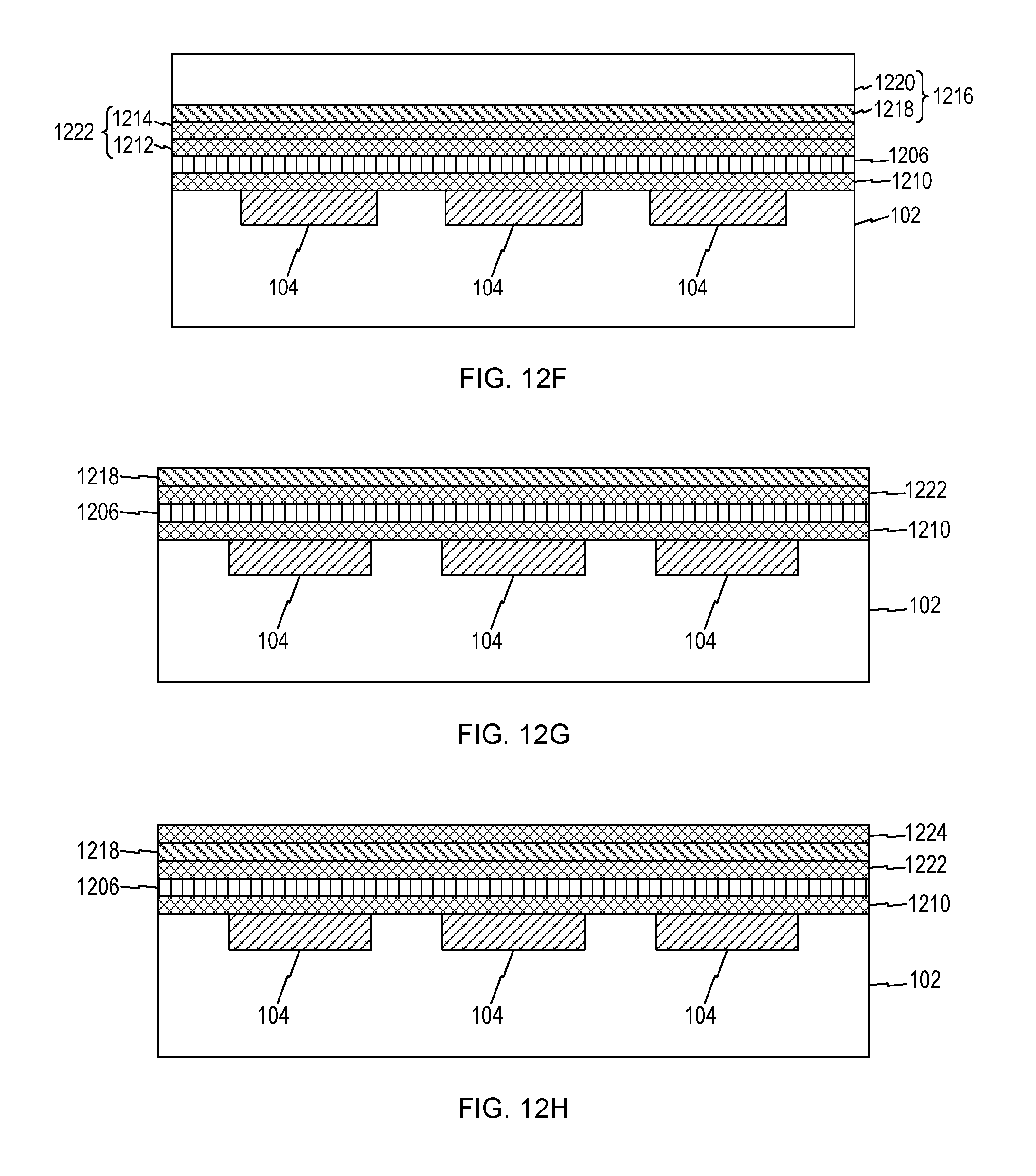
D00013

D00014

D00015
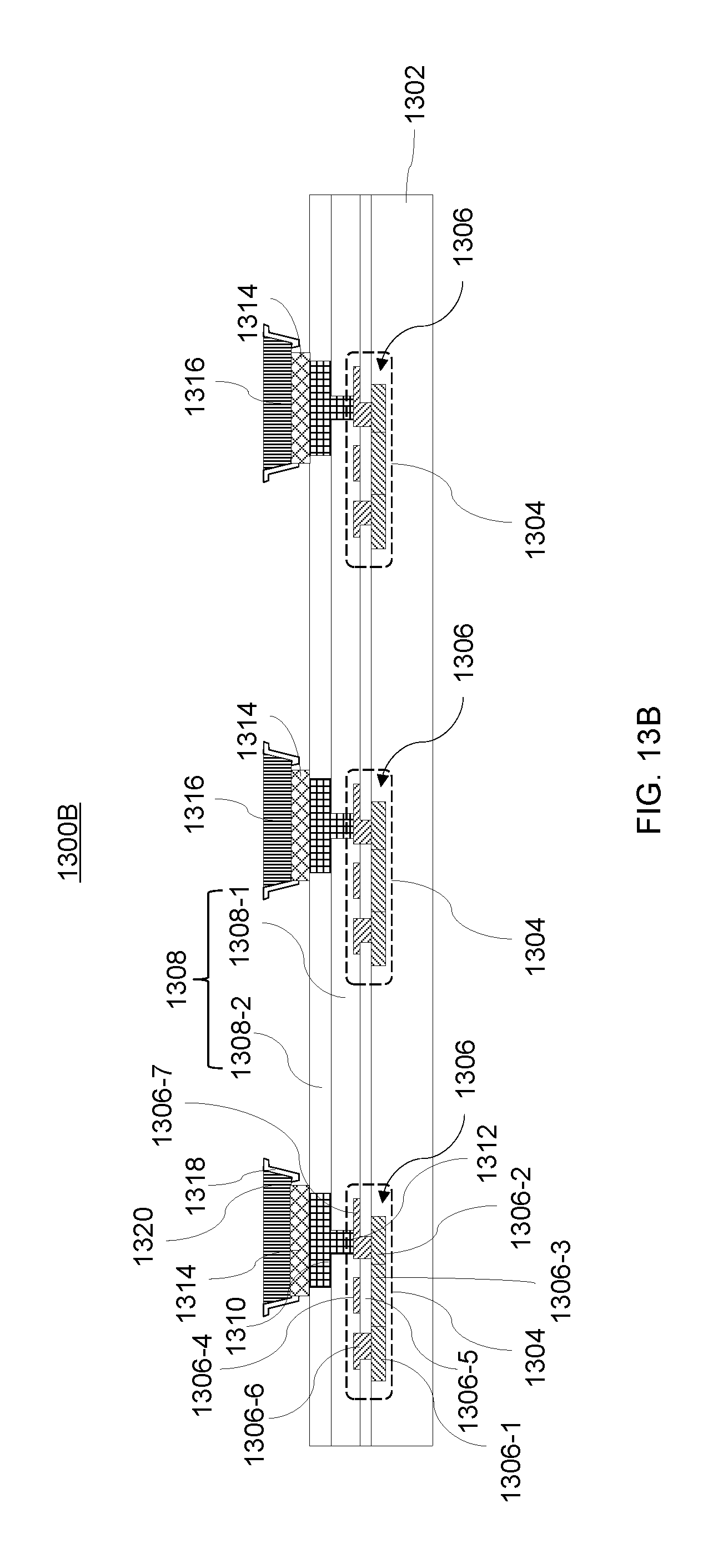
XML
uspto.report is an independent third-party trademark research tool that is not affiliated, endorsed, or sponsored by the United States Patent and Trademark Office (USPTO) or any other governmental organization. The information provided by uspto.report is based on publicly available data at the time of writing and is intended for informational purposes only.
While we strive to provide accurate and up-to-date information, we do not guarantee the accuracy, completeness, reliability, or suitability of the information displayed on this site. The use of this site is at your own risk. Any reliance you place on such information is therefore strictly at your own risk.
All official trademark data, including owner information, should be verified by visiting the official USPTO website at www.uspto.gov. This site is not intended to replace professional legal advice and should not be used as a substitute for consulting with a legal professional who is knowledgeable about trademark law.