| PTO- 1478 |
| Approved for use through 10/31/2024. OMB 0651-0009 |
| U.S. Patent and Trademark Office; U.S. DEPARTMENT OF COMMERCE Under the Paperwork Reduction Act of 1995, no persons are required to respond to a collection of information unless it contains a valid OMB control number |
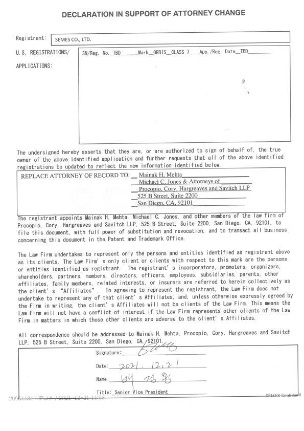
| Serial Number: 97187084 |
| Filing Date: 12/23/2021 |
| Input Field |
Entered |
| SERIAL NUMBER | 97187084 |
|---|---|
| MARK INFORMATION | |
| *MARK | \\TICRS\EXPORT18\IMAGEOUT 18\971\870\97187084\xml1 \ APP0002.JPG |
| SPECIAL FORM | YES |
| USPTO-GENERATED IMAGE | NO |
| LITERAL ELEMENT | ORBIS |
| COLOR MARK | NO |
| *DESCRIPTION OF THE MARK (and Color Location, if applicable) |
The mark consists of the wording ORBIS in a stylized font. |
| PIXEL COUNT ACCEPTABLE | YES |
| PIXEL COUNT | 944 x 250 |
| REGISTER | Principal |
| APPLICANT INFORMATION | |
| *OWNER OF MARK | Semes Co., Ltd. |
| *MAILING ADDRESS | 77 4sandan 5-gil Jiksan-eup Seobuk-gu |
| *CITY | Cheonan-si |
| *COUNTRY/REGION/JURISDICTION/U.S. TERRITORY | Korea, South |
| *ZIP/POSTAL CODE (Required for U.S. and certain international addresses) |
Chungcheongnam-do31040 |
| *EMAIL ADDRESS | XXXX |
| LEGAL ENTITY INFORMATION | |
| TYPE | limited liability company |
| STATE/COUNTRY/REGION/JURISDICTION/U.S. TERRITORY WHERE LEGALLY ORGANIZED | Korea, South |
| GOODS AND/OR SERVICES AND BASIS INFORMATION | |
| INTERNATIONAL CLASS | 007 |
| *IDENTIFICATION | apparatus for processing substrate; deposition apparatus for processing substrate; cleaning apparatus for processing substrate; drying apparatus for processing substrate; developing apparatus for processing substrate; coating apparatus for processing substrate; substrate transfer robot; substrates processing apparatus using plasma; plasma etching machines; dry etching apparatus; etching apparatus; plasma etching apparatus; plasma deposition apparatus; atomic layer deposition(ALD) apparatus for manufacturing semiconductors; atomic layer etching(ALE) apparatus for manufacturing semiconductors; apparatus for manufacturing semiconductors; machines for manufacturing semiconductors; semiconductor wafer cleaning apparatus; semiconductor wafer etching apparatus; semiconductor wafer drying apparatus; semiconductor wafer developing apparatus; semiconductor wafer coating apparatus; plasma etching apparatus for manufacturing semiconductors; plasma deposition apparatus for manufacturing semiconductors; etching apparatus for manufacturing semiconductors; plasma etching apparatus for manufacturing semiconductor wafers |
| FILING BASIS | SECTION 1(b) |
| FILING BASIS | SECTION 44(d) |
| FOREIGN APPLICATION NUMBER | 40-2021-0241261 |
| FOREIGN APPLICATION COUNTRY/REGION/JURISDICTION/U.S. TERRITORY |
Korea, South |
| FOREIGN FILING DATE | 11/26/2021 |
| INTENT TO PERFECT 44(d) |
At this time, the applicant has another basis for registration (Section 1(a) or Section 1(b)) and does NOT intend to rely on Section 44(e) as the basis for registration, but is only asserting a valid claim of priority. |
| ADDITIONAL STATEMENTS SECTION | |
| MISCELLANEOUS FILE NAME(S) | |
| ORIGINAL PDF FILE | MIS-209242145130-20211222 183521346231_._SIT210918U S_POA.pdf |
| CONVERTED PDF FILE(S) (1 page) |
\\TICRS\EXPORT18\IMAGEOUT 18\971\870\97187084\xml1\ APP0003.JPG |
| ATTORNEY INFORMATION | |
| NAME | Michael C. Jones |
| ATTORNEY DOCKET NUMBER | 12229611US01 |
| ATTORNEY BAR MEMBERSHIP NUMBER | XXX |
| YEAR OF ADMISSION | XXXX |
| U.S. STATE/ COMMONWEALTH/ TERRITORY | XX |
| FIRM NAME | Procopio, Cory, Hargreaves & Savitch LLP |
| STREET | 525 B Street, Suite 2200 |
| CITY | San Diego |
| STATE | California |
| COUNTRY/REGION/JURISDICTION/U.S. TERRITORY | United States |
| ZIP/POSTAL CODE | 92101 |
| PHONE | 650-645-9012 |
| FAX | 650-687-8303 |
| EMAIL ADDRESS | docketing@procopio.com |
| OTHER APPOINTED ATTORNEY | Mainak H. Mehta |
| CORRESPONDENCE INFORMATION | |
| NAME | Michael C. Jones |
| PRIMARY EMAIL ADDRESS FOR CORRESPONDENCE | docketing@procopio.com |
| SECONDARY EMAIL ADDRESS(ES) (COURTESY COPIES) | michael.jones@procopio.com; miku.mehta@procopio.com; patentteam@procopio.com; cailin.musgrove@procopio.com |
| FEE INFORMATION | |
| APPLICATION FILING OPTION | TEAS Standard |
| NUMBER OF CLASSES | 1 |
| APPLICATION FOR REGISTRATION PER CLASS | 350 |
| *TOTAL FEES DUE | 350 |
| *TOTAL FEES PAID | 350 |
| SIGNATURE INFORMATION | |
| SIGNATURE | /Michael C. Jones/ |
| SIGNATORY'S NAME | Michael C. Jones |
| SIGNATORY'S POSITION | Attorney of Record, State of California Bar Member |
| SIGNATORY'S PHONE NUMBER | 650-645-9012 |
| DATE SIGNED | 12/22/2021 |
| SIGNATURE METHOD | Sent to third party for signature |
| PTO- 1478 |
| Approved for use through 10/31/2024. OMB 0651-0009 |
| U.S. Patent and Trademark Office; U.S. DEPARTMENT OF COMMERCE Under the Paperwork Reduction Act of 1995, no persons are required to respond to a collection of information unless it contains a valid OMB control number |
| Serial Number: 97187084 |
| Filing Date: 12/23/2021 |
| The applicant's current Correspondence Information: |
| Michael C. Jones |
| PRIMARY EMAIL FOR CORRESPONDENCE: docketing@procopio.com SECONDARY EMAIL ADDRESS(ES) (COURTESY COPIES): michael.jones@procopio.com; miku.mehta@procopio.com; patentteam@procopio.com; cailin.musgrove@procopio.com Requirement for Email and Electronic Filing: I understand that a valid email address must be maintained by the applicant owner/holder and the applicant owner's/holder's attorney, if appointed, and that all official trademark correspondence must be submitted via the Trademark Electronic Application System (TEAS). |
|
|
|