| To: | Fairchild Semiconductor Corporation (trademark@pierceatwood.com) |
| Subject: | U.S. TRADEMARK APPLICATION NO. 85952677 - RAZOR - 17732-4723 |
| Sent: | 4/9/2014 3:50:36 PM |
| Sent As: | ECOM110@USPTO.GOV |
| Attachments: | Attachment - 1 Attachment - 2 Attachment - 3 Attachment - 4 Attachment - 5 Attachment - 6 Attachment - 7 Attachment - 8 Attachment - 9 Attachment - 10 Attachment - 11 Attachment - 12 Attachment - 13 Attachment - 14 Attachment - 15 Attachment - 16 |
UNITED STATES PATENT AND TRADEMARK OFFICE (USPTO)
OFFICE ACTION (OFFICIAL LETTER) ABOUT APPLICANT’S TRADEMARK APPLICATION
|
U.S. APPLICATION SERIAL NO. 85952677
MARK: RAZOR
|
|
|
CORRESPONDENT ADDRESS: |
CLICK HERE TO RESPOND TO THIS LETTER: http://www.gov.uspto.report/trademarks/teas/response_forms.jsp
|
|
APPLICANT: Fairchild Semiconductor Corporation
|
|
|
CORRESPONDENT’S REFERENCE/DOCKET NO: CORRESPONDENT E-MAIL ADDRESS: |
|
OFFICE ACTION
TO AVOID ABANDONMENT OF APPLICANT’S TRADEMARK APPLICATION, THE USPTO MUST RECEIVE APPLICANT’S COMPLETE RESPONSE TO THIS LETTER WITHIN 6 MONTHS OF THE ISSUE/MAILING DATE BELOW.
ISSUE/MAILING DATE: 4/9/2014
THIS IS A FINAL ACTION.
This Office action is in response to applicant’s communication filed on March 19, 2014.
In a previous Office action(s) dated September 19, 2013, the trademark examining attorney refused registration of the applied-for mark under Trademark Act Section 2(d).
Based on applicant’s response, the trademark examining attorney maintains and now makes FINAL the refusal(s) and/or requirement(s) in the summary of issues below. See 37 C.F.R. §2.64(a); TMEP §714.04.
SUMMARY OF ISSUES MADE FINAL that applicant must address:
SECTION 2(d) REFUSAL – LIKELIHOOD OF CONFUSION – Refusal Made FINAL
In this case, the following factors are the most relevant: similarity of the marks, similarity and nature of the goods and/or services, and similarity of the trade channels of the goods and/or services. See In re Viterra Inc., 671 F.3d 1358, 1361-62, 101 USPQ2d 1905, 1908 (Fed. Cir. 2012); In re Dakin’s Miniatures Inc., 59 USPQ2d 1593, 1595-96 (TTAB 1999); TMEP §§1207.01 et seq.
The proposed mark is RAZOR for Semiconductor devices excluding light emitting diodes, photodiodes, laser diodes and silicon carbide semiconductor wafers. The registered mark is RAZERTHIN for Optoelectronic devices, namely, light emitting diodes, photodiodes, laser diodes, silicon carbide semiconductor wafers (relevant part underlined).
As stated previously, the applicant’s proposed mark is composed in its entirety of the single term RAZOR. The registrant’s mark is RAZERTHIN. Therefore, both marks share the similar sounding terms, RAZOR/RAZER. Marks may be confusingly similar in appearance where there are similar terms or phrases or similar parts of terms or phrases appearing in both applicant’s and registrant’s mark. See Crocker Nat’l Bank v. Canadian Imperial Bank of Commerce, 228 USPQ 689 (TTAB 1986), aff’d sub nom. Canadian Imperial Bank of Commerce v. Wells Fargo Bank, Nat’l Ass’n, 811 F.2d 1490, 1 USPQ2d 1813 (Fed. Cir. 1987) (COMMCASH and COMMUNICASH); In re Phillips-Van Heusen Corp., 228 USPQ 949 (TTAB 1986) (21 CLUB and “21” CLUB (stylized)); In re Corning Glass Works, 229 USPQ 65 (TTAB 1985) (CONFIRM and CONFIRMCELLS); In re Collegian Sportswear Inc., 224 USPQ 174 (TTAB 1984) (COLLEGIAN OF CALIFORNIA and COLLEGIENNE); In re Pellerin Milnor Corp., 221 USPQ 558 (TTAB 1983) (MILTRON and MILLTRONICS); In re BASF A.G., 189 USPQ 424 (TTAB 1975) (LUTEXAL and LUTEX); TMEP §1207.01(b)(ii)-(iii).
In addition to the initial term, RAZER, the registrant’s mark includes the additional term THIN, which is merely descriptive, as indicated by that mark being on the Supplemental Register. So the applicant's and registrant’s marks are essentially the same except for the deletion of THIN in the applicant’s mark. The mere deletion of wording from a registered mark may not be sufficient to overcome a likelihood of confusion. See In re Mighty Leaf Tea, 601 F.3d 1342, 94 USPQ2d 1257 (Fed. Cir. 2010); In re Optica Int’l, 196 USPQ 775, 778 (TTAB 1977); TMEP §1207.01(b)(ii)-(iii).
With regard to commercial impression of the two marks, they are not identical, but they are highly similar. Specifically, the registrant’s mark, RAZERTHIN, is registered on the Supplemental Register, because the terms describe a feature or characteristic of the registrant’s semiconductor wafers and other recited goods being as thin as a razor or razor blade. Although the applicant’s proposed mark, RAZOR, alone may not immediately bring to mind the thickness of the applicant’s goods, those familiar with the types of goods at issue in these two cases, e.g., semiconductors and semiconductor wafers, are aware that these goods must be very thin in order to be placed on a semiconductor and be used for their intended purposes. Arguably, a consumer of these particular goods, encountering these proposed marks in the marketplace, would be likely to conjure up a similar image for each mark.
Applicant’s mark does not create a distinct commercial impression because it contains the same common wording as registrant’s mark, and there is no other wording to distinguish it from registrant’s mark.
The respective goods and/or services need only be “related in some manner and/or if the circumstances surrounding their marketing [be] such that they could give rise to the mistaken belief that [the goods and/or services] emanate from the same source.” Coach Servs., Inc. v. Triumph Learning LLC, 668 F.3d 1356, 1369, 101 USPQ2d 1713, 1722 (Fed. Cir. 2012) (quoting 7-Eleven Inc. v. Wechsler, 83 USPQ2d 1715, 1724 (TTAB 2007)); Gen. Mills Inc. v. Fage Dairy Processing Indus. SA, 100 USPQ2d 1584, 1597 (TTAB 2011); TMEP §1207.01(a)(i).
In the instant case, the applicant proposes use of their mark on Semiconductor devices excluding light emitting diodes, photodiodes, laser diodes and silicon carbide semiconductor wafers, and the registrant uses their mark on Optoelectronic devices, namely, light emitting diodes, photodiodes, laser diodes, silicon carbide semiconductor wafers. In particular, the most relevant goods in these two cases are the semiconductor devices (applicant) and silicon carbide semiconductor wafers (registrant). Essentially, the semiconductor wafers produced by the registrant are the base on which the remaining semiconductor and integrated circuit is formed or “built.” See below:
“A silicon wafer consists of a thin slice of silicon which can be treated in various ways, depending on the type of electronics it is being used in. Silicon is a very high quality semiconductor, making it ideal for the production of such circuits.” http://www.wisegeek.com/what-are-silicon-wafers.htm.
“The heart of semiconductor manufacturing is the wafer fabrication facility where the integrated circuit is formed in and on the wafer.” http://rel.intersil.com/docs/lexicon/manufacture.html.
“In the Front-End operation, a blank wafer, typically silicon, is the start of the process. Essentially, semiconductor manufacturing uses chemicals to create circuits by adding and removing layers on the wafer.” http://www.nxp.com/about/corporate-social-responsibility/sustainability/semiconductor-manufacturing.html.
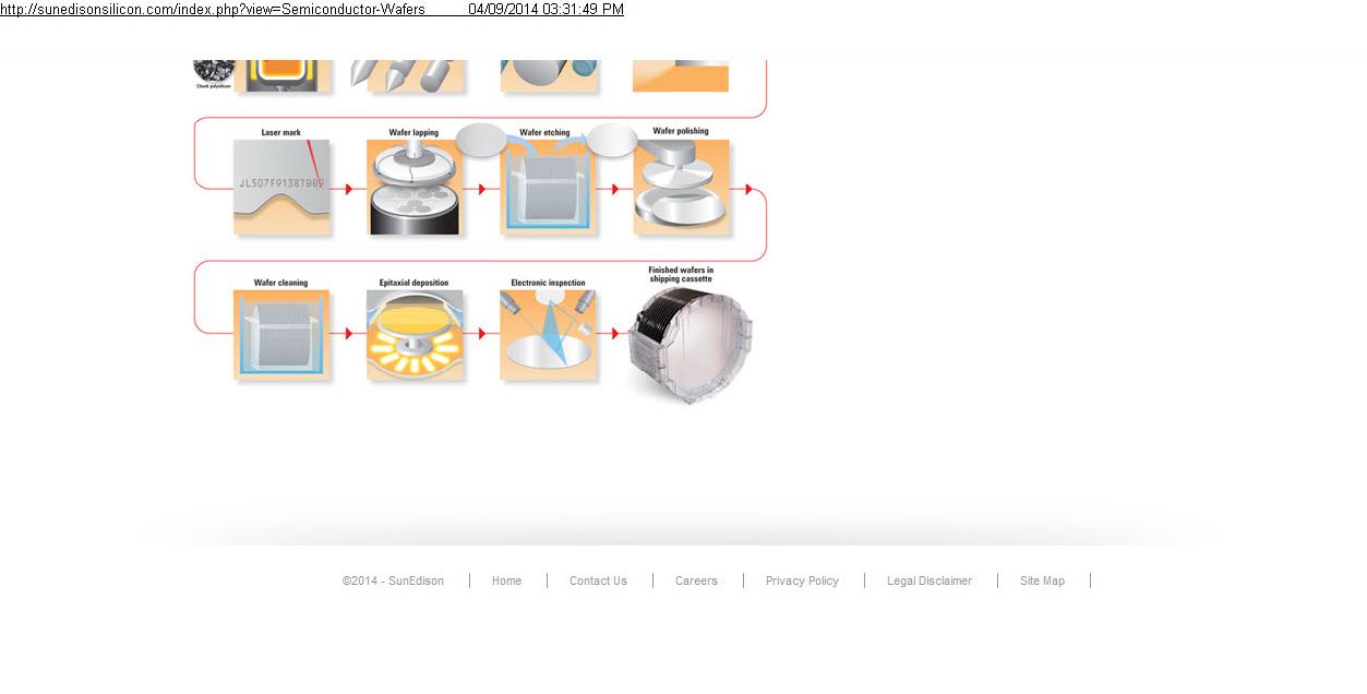
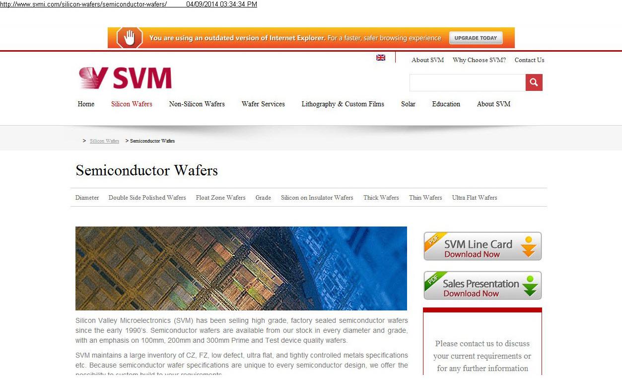
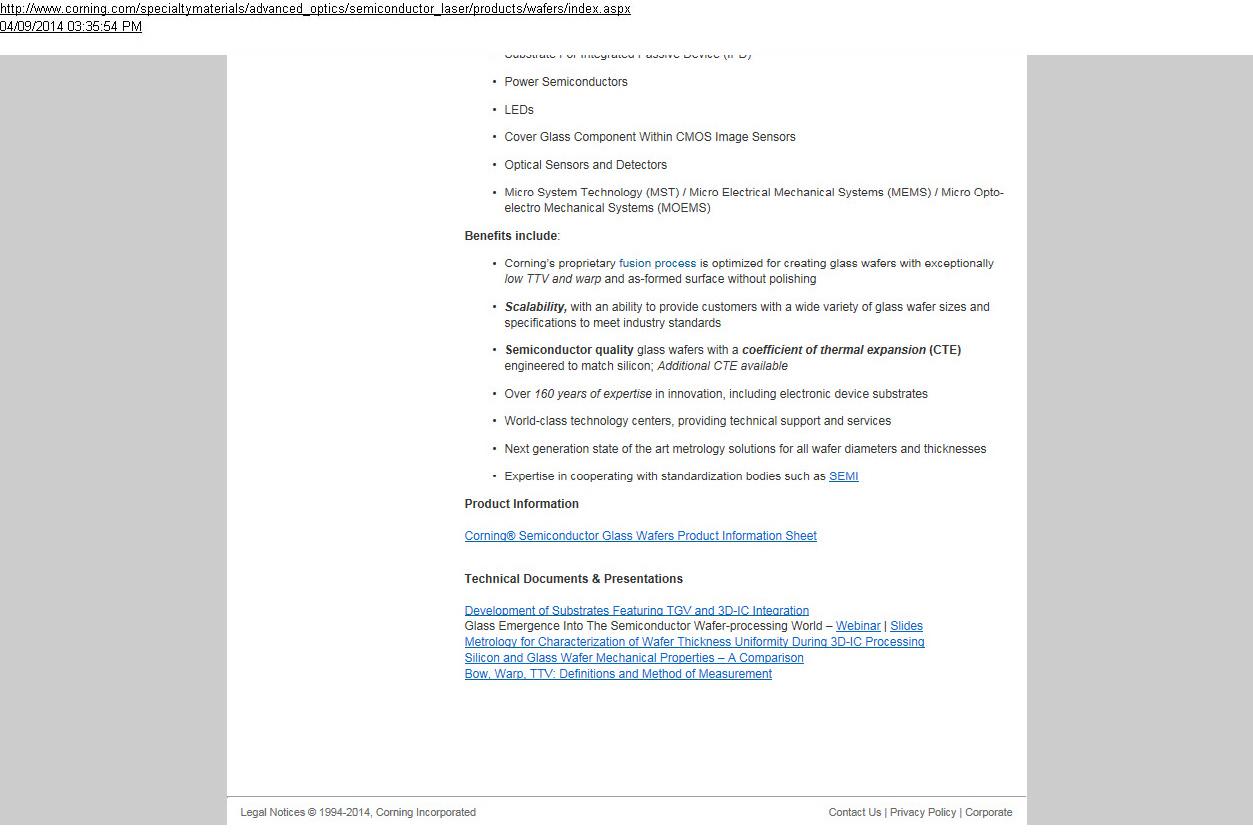
See also http://sunedisonsilicon.com/index.php?view=Semiconductor-Wafers; http://www.svmi.com/silicon-wafer-manufacturing-semiconductor-process/; http://www.svmi.com/silicon-wafers/semiconductor-wafers/; www.corning.com/specialtywafers/advanced_optics/semiconductor_laser/products/wafers/index.aspx.
Therefore, the applicant’s semiconductor devices cannot be manufactured without a semiconductor wafer, most often formed from silicon material, as the starting block. Thus, the applicant’s and registrant’s goods are really significantly entwined and related to each other, regardless of the applicant’s negative limitations excluding the exact goods recited by the registrant. In other words, the applicant’s goods and registrant’s goods are related despite the exclusion of the specific goods recited by the registrant from the applicant’s identification of goods. The applicant is still intending to use the proposed mark on other semiconductor devices, which would be directly and closely related to the registrant’s silicon carbide semiconductor wafers, at least.
Applicant’s arguments have been considered and found unpersuasive for the reason(s) set forth below.
The applicant argues that the proposed mark RAZOR and the cited mark RAZERTHIN “convey significantly different commercial impression[s] because of the deletion of the word THIN.” Response to Office action of 3/19/14, Attachments, page 2. The applicant further argues that “this is especially true given the descriptive nature of the cited RAZERTHIN mark.” Id., Attachments, page 3. Both of these arguments have been addressed above in the trademark examining attorney’s explanation of the similarities between the applicant’s and registrant’s marks. Therefore, this argument is not convincing.
The only other argument presented by the applicant is that the amended identification of goods, specifically excluding those goods recited by the registrant, “further establish[es] that there is no likelihood of confusion.” Id. This argument has also been addressed above in the explanation of the similarities of the goods and their relatedness. Therefore, this argument is similarly not convincing.
For all of the reasons discussed above, the refusal of the applicant’s proposed mark under Section 2(d) of the Trademark Act is maintained and made FINAL.
RESPONSE TO FINAL ACTION
(1) Submitting a response that fully satisfies all outstanding requirements, if feasible; and/or
(2) Filing an appeal to the Trademark Trial and Appeal Board, with an appeal fee of $100 per class.
37 C.F.R. §§2.6(a)(18), 2.64(a); TBMP ch. 1200; TMEP §714.04.
In certain rare circumstances, a petition to the Director may be filed pursuant to 37 C.F.R. §2.63(b)(2) to review a final Office action that is limited to procedural issues. 37 C.F.R. §2.64(a); TMEP §714.04; see 37 C.F.R. §2.146(b); TBMP §1201.05; TMEP §1704 (explaining petitionable matters). The petition fee is $100. 37 C.F.R. §2.6(a)(15).
If applicant has questions regarding this Office action, please telephone or e-mail the assigned trademark examining attorney. All relevant e-mail communications will be placed in the official application record; however, an e-mail communication will not be accepted as a response to this Office action and will not extend the deadline for filing a proper response. See 37 C.F.R. §2.191; TMEP §§709.04-.05. Further, although the trademark examining attorney may provide additional explanation pertaining to the refusal(s) and/or requirement(s) in this Office action, the trademark examining attorney may not provide legal advice or statements about applicant’s rights. See TMEP §§705.02, 709.06.
/Jennifer Hazard Dixon/
Trademark Examining Attorney
Law Office 110
571-272-9359
jennifer.dixon@uspto.gov
(emailed responses not accepted)
TO RESPOND TO THIS LETTER: Go to http://www.gov.uspto.report/trademarks/teas/response_forms.jsp. Please wait 48-72 hours from the issue/mailing date before using the Trademark Electronic Application System (TEAS), to allow for necessary system updates of the application. For technical assistance with online forms, e-mail TEAS@uspto.gov. For questions about the Office action itself, please contact the assigned trademark examining attorney. E-mail communications will not be accepted as responses to Office actions; therefore, do not respond to this Office action by e-mail.
All informal e-mail communications relevant to this application will be placed in the official application record.
WHO MUST SIGN THE RESPONSE: It must be personally signed by an individual applicant or someone with legal authority to bind an applicant (i.e., a corporate officer, a general partner, all joint applicants). If an applicant is represented by an attorney, the attorney must sign the response.
PERIODICALLY CHECK THE STATUS OF THE APPLICATION: To ensure that applicant does not miss crucial deadlines or official notices, check the status of the application every three to four months using the Trademark Status and Document Retrieval (TSDR) system at http://tsdr.gov.uspto.report/. Please keep a copy of the TSDR status screen. If the status shows no change for more than six months, contact the Trademark Assistance Center by e-mail at TrademarkAssistanceCenter@uspto.gov or call 1-800-786-9199. For more information on checking status, see http://www.gov.uspto.report/trademarks/process/status/.
TO UPDATE CORRESPONDENCE/E-MAIL ADDRESS: Use the TEAS form at http://www.gov.uspto.report/trademarks/teas/correspondence.jsp.