| To: | Advanced Chip Engineering Technology Inc ETC. (mailroom@bskb.com) |
| Subject: | TRADEMARK APPLICATION NO. 78475959 - CSP - 4444-0157US1 |
| Sent: | 4/25/05 10:47:31 AM |
| Sent As: | ECOM106@USPTO.GOV |
| Attachments: | Attachment - 1 Attachment - 2 Attachment - 3 Attachment - 4 |
UNITED STATES PATENT AND TRADEMARK OFFICE
|
SERIAL NO: 78/475959
APPLICANT: Advanced Chip Engineering Technology Inc ETC.
|
|
|
CORRESPONDENT ADDRESS: |
RETURN ADDRESS: Commissioner for Trademarks P.O. Box 1451 Alexandria, VA 22313-1451
|
|
MARK: CSP
|
|
|
CORRESPONDENT’S REFERENCE/DOCKET NO: 4444-0157US1
CORRESPONDENT EMAIL ADDRESS: |
Please provide in all correspondence:
1. Filing date, serial number, mark and applicant's name. 2. Date of this Office Action. 3. Examining Attorney's name and Law Office number. 4. Your telephone number and e-mail address.
|
Serial Number 78/475959
This Office Action is supplemental to the previous Office Action dated 4/11/05, and incorporates all outstanding issues there from.
Applicant must disclaim the descriptive wording “CSP” apart from the mark as shown because it merely describes a feature of applicant’s goods. Trademark Act Section 6, 15 U.S.C. §1056; TMEP §§1213 and 1213.03(a).
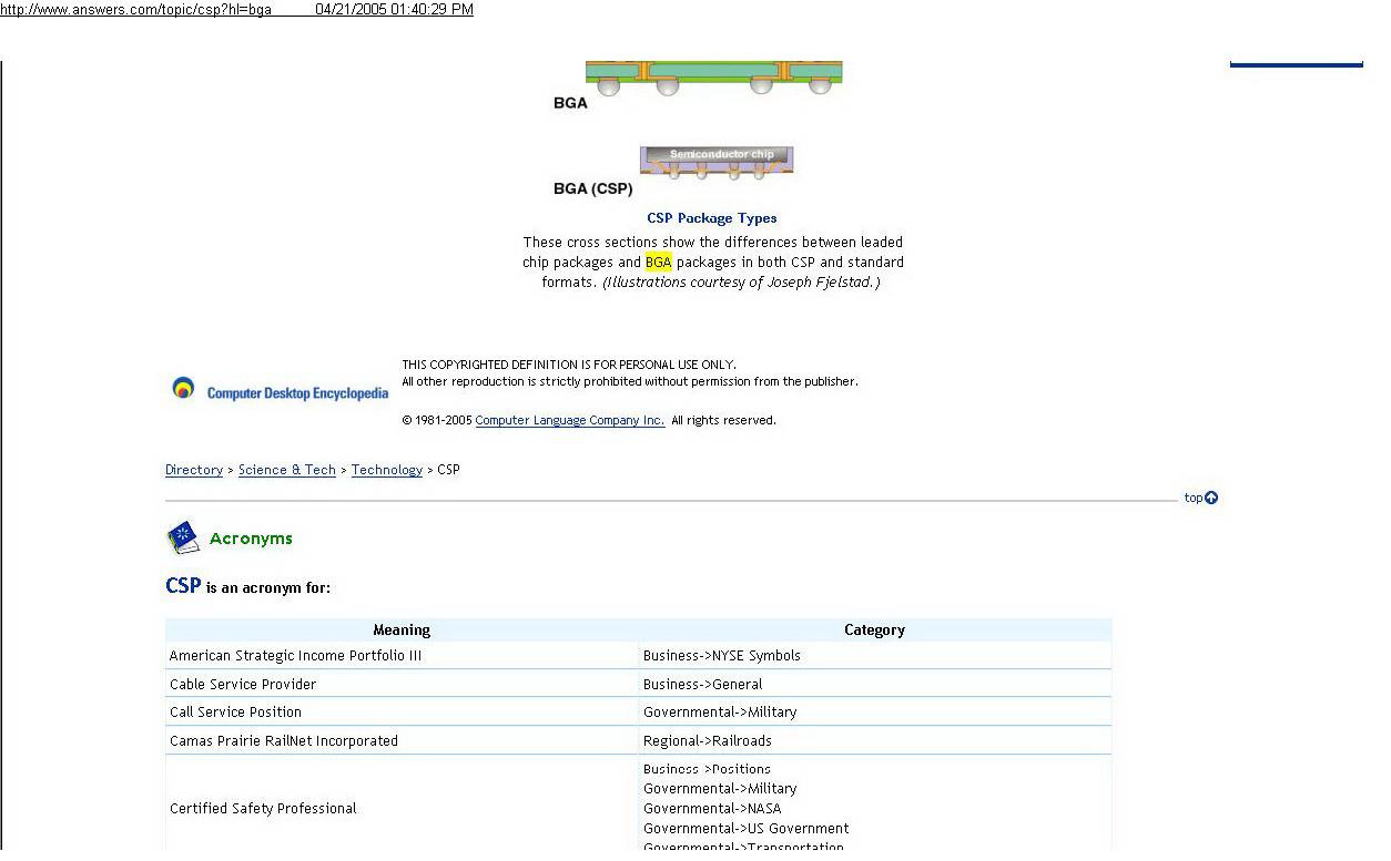
The wording “CSP” is an acronym for “Chip Scale Package” or “Chip Size Package” in the computer chip industry, which is defined, “A chip housing that is slightly larger than the chip itself. More than 100 types of CSP packages have been developed, mostly using BGA mounting.” (See attached evidence “csp.”) Applicant’s goods for “Floating-point operation chip; ROM (Read Only Memory chip); Structured semi-conductor wafers; Memory cards, computer hardware; Flash memory card; RAM (Random Access Memory) card; Semi-conductor memory units; Blank electronic chip cards, namely, blank smart cards; Encoded electronic chip cards, namely, smart cards containing programming used to specify the function or purpose and, if the programming is content or field specific, the field of use; Semiconductor chips; Semiconductor devices; Semiconductor power elements; Micro-circuit; Silicon chips; Integrated circuit; Microprocessors unit chips; ULSI (Ultra Large Scale Integration; VLSI (Very Large Scale Integration); Silicon wafers; Wafers” include many varieties of computer chips. Thus the wording “CSP” is descriptive of applicant’s goods and must be disclaimed.
This Office Action resets the 6-month period for response for all requirements and refusals included in this Office Action and the Office Action dated 4/11/05.
Effective January 31, 2005 and pursuant to the Consolidated Appropriations Act, 2005, Pub. L. 108-447, the following are the fees that will be charged for filing a trademark application:
(1) $325 per international class if filed electronically using the Trademark Electronic Application System (TEAS); or
(2) $375 per international class if filed on paper
These fees will be charged not only when a new application is filed, but also when payments are made to add classes to an existing application. If such payments are submitted with a TEAS response, the fee will be $325 per class, and if such payments are made with a paper response, the fee will be $375 per class.
The new fee requirements will apply to any fees filed on or after January 31, 2005.
NOTICE: TRADEMARK OPERATION RELOCATION
The Trademark Operation has relocated to Alexandria, Virginia. Effective October 4, 2004, all Trademark-related paper mail (except documents sent to the Assignment Services Division for recordation, certain documents filed under the Madrid Protocol, and requests for copies of trademark documents) must be sent to:
Commissioner for Trademarks
P.O. Box 1451
Alexandria, VA 22313-1451
Applicants, attorneys and other Trademark customers are strongly encouraged to correspond with the USPTO online via the Trademark Electronic Application System (TEAS), at http://www.gov.uspto.report/teas/index.html.
Ada P. Han
/Ada P. Han/
Trademark Attorney
Law Office 106
(571) 272-5873
(571) 273-9106 (fax)
HOW TO RESPOND TO THIS OFFICE ACTION:
STATUS OF APPLICATION: To check the status of your application, visit the Office’s Trademark Applications and Registrations Retrieval (TARR) system at http://tarr.uspto.gov.
VIEW APPLICATION DOCUMENTS ONLINE: Documents in the electronic file for pending applications can be viewed and downloaded online at http://portal.gov.uspto.report/external/portal/tow.
GENERAL TRADEMARK INFORMATION: For general information about trademarks, please visit the Office’s website at http://www.gov.uspto.report/main/trademarks.htm
FOR INQUIRIES OR QUESTIONS ABOUT THIS OFFICE ACTION, PLEASE CONTACT THE ASSIGNED EXAMINING ATTORNEY SPECIFIED ABOVE.